HCC4543B
HCF4543B
December 1989
BCD-TO-7 SEGMENT LATCH/DECODER/LCD DRIVER
EY
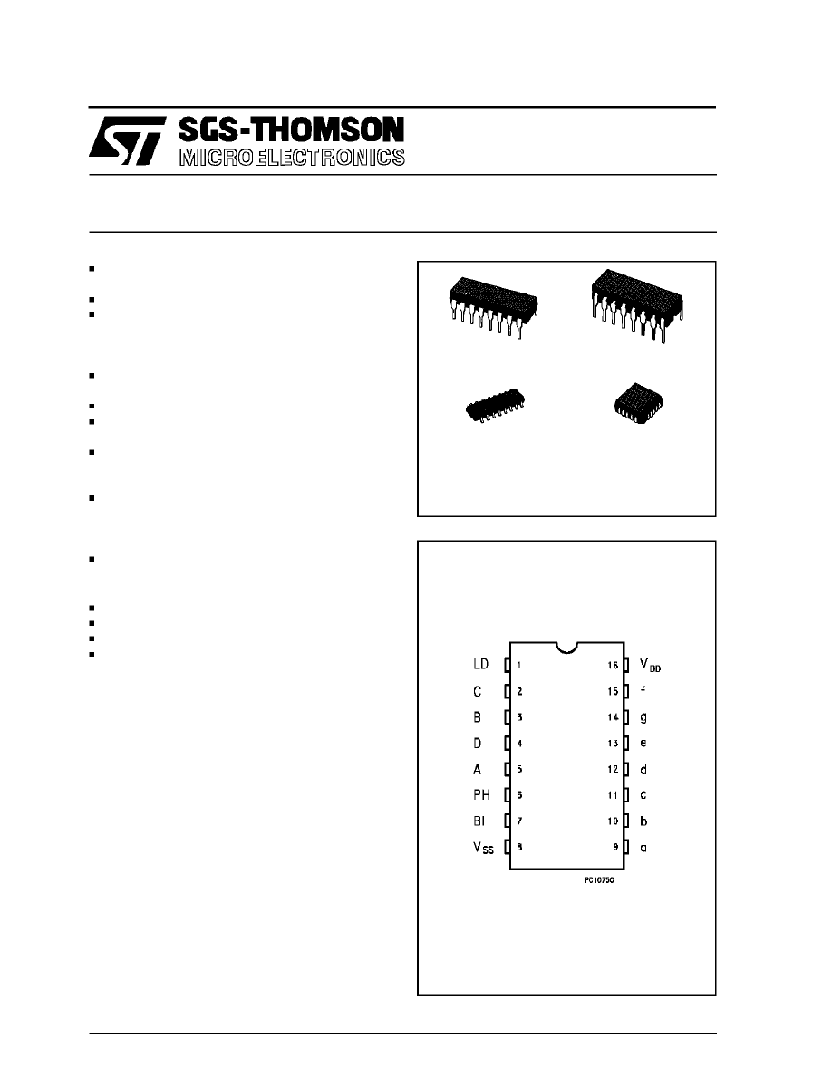
(Plastic Package)
DISPLAY BLANKING OF ALL ILLEGAL INPUT
COMBINATIONS
LATCH STORAGE OF CODE
CAPABILITY OF DRIVING TWO LOW POWER
TTL LOADS, TWO HTL LOADS, OR ONE LOW
POWER SCHOTTKY LOAD OVER THE FULL
RATED-TEMPERATURE RANGE
PIN-FOR-PIN
REPLACEMENT
FOR
THE
HCF4056B (with pin 7 tied to V
SS
)
DIRECT LED DRIVING CAPABILITY
100% TESTED FOR QUIESCENT CURRENT
AT 20V
MAXIMUM INPUT CURRENT OF 1A AT 18V
OVER
FULL
PACKAGE-TEMPERATURE
RANGE ; 100nA AT 18V AND 25
°
C
NOISE MARGIN (full package-temperature
range) = 1V AT V
DD
= 5V
2V AT V
DD
= 10V
2.5V AT V
DD
= 15V
5-V, 10-V, AND 15-V PARAMETRIC RATINGS
ORDER CODES :
HCC4543 BF
HCF4543 BM1
HCF4543 BEY
HCF4543 BC1
F
(Ceramic Frit Seal Package)
M1
(Micro Package)
C1
(Plastic Chip Carrier)
Applications :
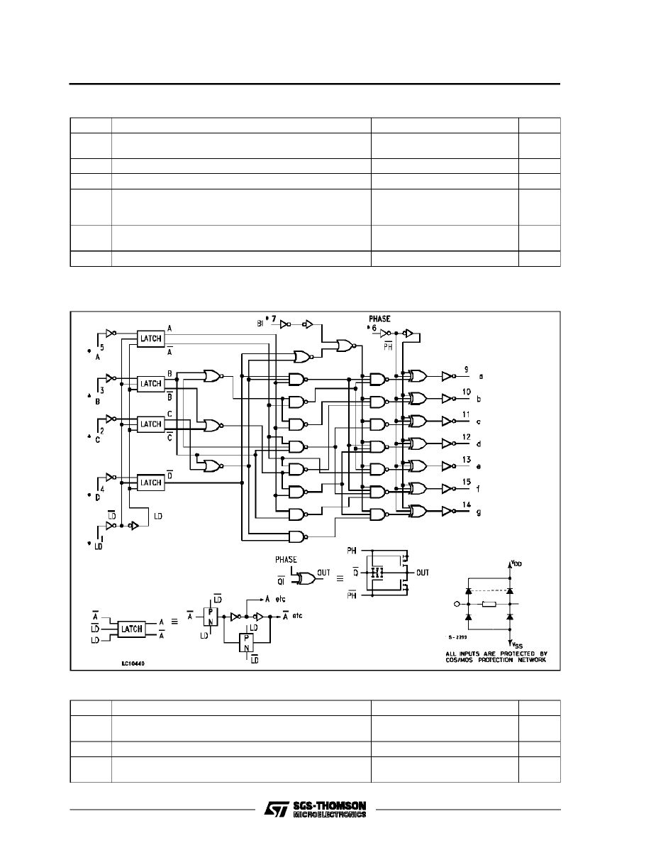
PIN CONNECTION (top view)
INSTRUMENT DISPLAY DRIVER
DASHBOARD DISPLAY DRIVER
COMPUTER/CALCULATOR DISPLAY DRIVER
TIMING DEVICE DRIVER (clocks, watches,
timers)
DESCRIPTION
The HCC/HCF4543B is a BCD-to-seven segment
latch/decoder/driver designed primarily for liquid-
crystal display (LCD) applications. It is also capable
of driving light emitting diode (LED), incandescent,
gas-discharge, and fluorescent displays. This de-
vice is functionally similar to and serves as direct re-
placement for the HCF4056B when pin 7 is
connected to V
SS
. It differs from the HCF4056B in
that it has a display blanking capability instead of a
level-shifting function and requires only one power
supply. When the HCF4056B is used in the level
shifting mode, two power supplies are required.
When the HCF4543B is used for LCD applications,
a square wave must be applied to the PHASE input
and the backplane of the LCD device. For LED ap-
plications a logic 1 is required at the PHASE input
for common-cathode devices ; a logic 0 is required
for common-anode devices (see truth table).
HCC/HCF4543B
1/12
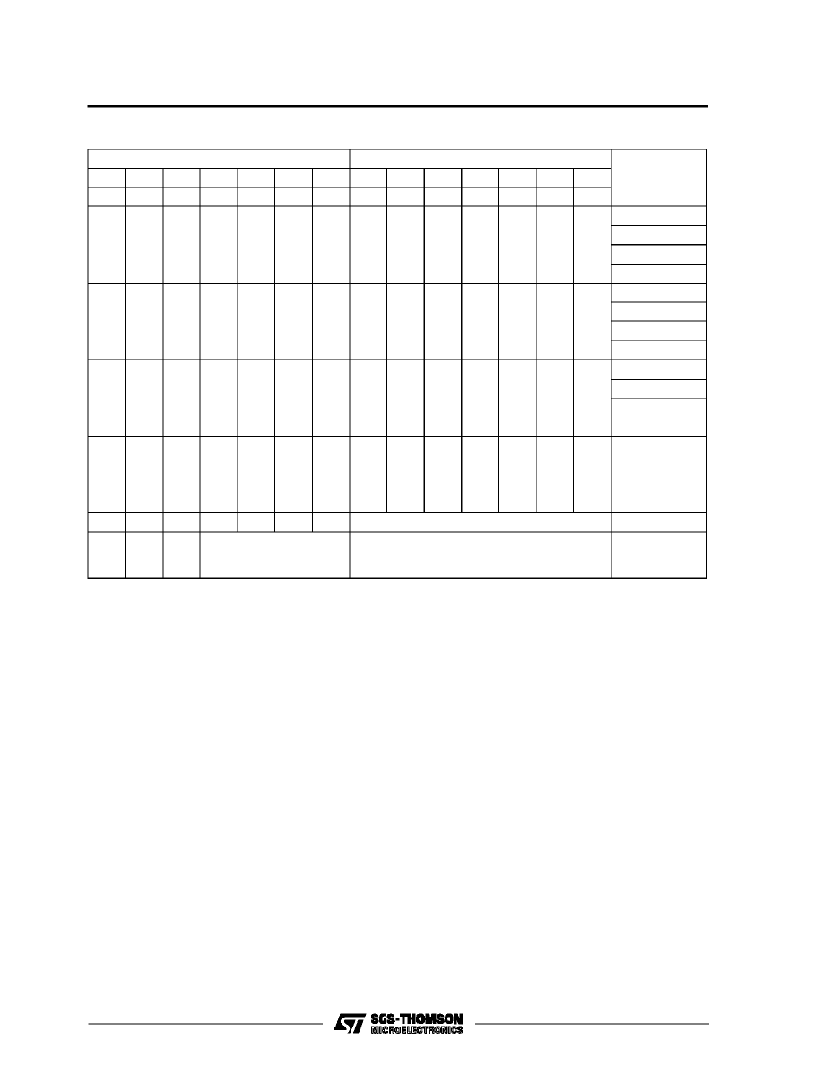
LOGIC DIAGRAM (1/2 of device shown)
Symbol
Parameter
Valu e
Unit
V
DD
*
Supply voltage :
HCC Types
HCF Types
– 0.5 to + 20
– 0.5 to 18
V
V
V
i
Input Voltage
– 0.5 to V
DD
+ 0.5
V
I
I
DC Input Current (any one input)
±
10
mA
P
tot
Total Power Dissipation (per package)
Dissipation per Output Transistor
for T
op
= Full Package-temperature Range
200
100
mW
mW
T
op
Operating Temperature : HCC Types
HCF Types
– 55 to + 125
– 40 to + 85
°
C
°
C
T
stg
Storage Temperature
– 65 to + 150
°
C
* All Voltage Values are referred to V
SS
pin voltage.
ABSOLUTE MAXIMUM RATINGS
RECOMMENDED OPERATING CONDITIONS
Symbol
Parameter
Valu e
Unit
V
DD
Supply Voltage :
HCC Types
HCF Types
3 to + 18
3 to + 15
V
V
V
I
Input Voltage
0 to V
DD
V
T
op
Operating Temperature : HCC Types
HCF Types
– 55 to + 125
– 40 to + 85
°
C
°
C
HCC/HCF4543B
2/12
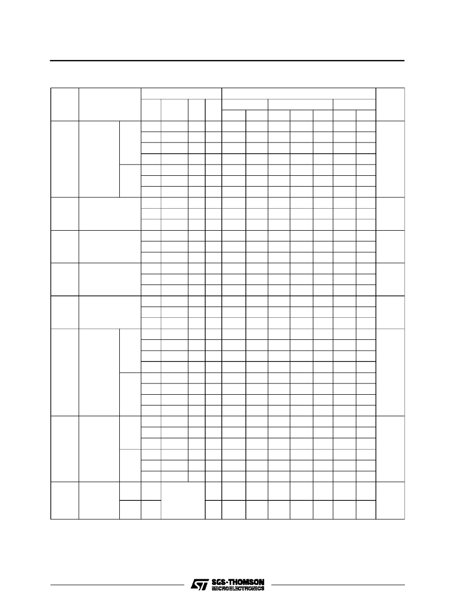
TRUTH TABLE
INPUT CODE
OUTPUT STATE
DI SPLAY
CHARACTER
LD
BI
Ph*
D
C
B
A
a
b
c
d
e
f
g
X
1
0
X
X
X
X
0
0
0
0
0
0
0
1
0
0
0
0
0
0
1
1
1
1
1
1
0
0
1
0
0
0
0
0
1
0
1
1
0
0
0
0
1
1
0
0
0
0
1
0
1
1
0
1
1
0
1
2
1
0
0
0
0
1
1
1
1
1
1
0
0
1
3
1
0
0
0
1
0
0
0
1
1
0
0
1
1
4
1
0
0
0
1
0
1
1
0
1
1
0
1
1
5
1
0
0
0
1
1
0
1
0
1
1
1
1
1
6
1
0
0
0
1
1
1
1
1
1
0
0
0
0
7
1
0
0
1
0
0
0
1
1
1
1
1
1
1
8
1
0
0
1
0
0
1
1
1
1
1
0
1
1
9
1
0
0
1
0
1
0
0
0
0
0
0
0
0
Blank
1
0
0
1
0
1
1
0
0
0
0
0
0
0
Blank
1
0
0
1
1
0
0
0
0
0
0
0
0
0
Blank
1
0
0
1
1
0
1
0
0
0
0
0
0
0
Blank
1
0
0
1
1
1
0
0
0
0
0
0
0
0
Blank
1
0
0
1
1
1
1
0
0
0
0
0
0
0
Blank
0
0
0
X
X
X
X
**
**
•
•
•
•
Inverse of Output
Combinations
Above
Display
as above
X = Don’t care.
•
= Above combinations
* = For liquid-crystal readouts, apply a square wave to Ph.
For common cathode LED readouts, select Ph = 0.
For common anode LED readouts, select Ph = 1.
** = Depends upon the BCD code previously applied when LD = 1.
HCC/HCF4543B
3/12
STATIC ELECTRICAL CHARACTERISTICS
Symbol
Parameter
Test Conditi ons
Value
Unit
V
I
(V)
V
O
(V)
I
O
(
µ
A)
V
DD
(V)
T
Low
25
°
C
T
High
Min.
Max.
Min.
Typ. Max.
Min. Max.
I
L
Quiescent
Current
HCC
Types
0/5
5
5
0.04
5
150
µ
A
0/10
10
10
0.04
10
300
0/15
15
20
0.04
20
600
0/20
20
100
0.08
100
3000
HCF
Types
0/5
5
5
0.04
5
150
0/10
10
10
0.04
10
300
0/15
15
20
0.04
20
600
V
OH
Output High
Voltage
0/5
< 1
5
4.95
4.95
4.95
V
0/10
< 1
10
9.95
9.95
9.95
0/15
< 1
15
14.95
14.95
14.95
V
OL
Output Low
Voltage
5/0
< 1
5
0.05
0.05
0.05
V
10/0
< 1
10
0.05
0.05
0.05
15/0
< 1
15
0.05
0.05
0.05
V
IH
Input High
Voltage
0.5/4.5
< 1
5
3.5
3.5
3.5
V
1/9
< 1
10
7
7
7
1.5/13.5 < 1
15
11
11
11
V
IL
Input Low
Voltage
4.5/0.5
< 1
5
1.5
1.5
1.5
V
9/1
< 1
10
3
3
3
13.5/1.5 < 1
15
4
4
4
I
OH
Output
Drive
Current
HCC
Types
0/5
2.5
5
– 1.6
– 1.3
– 2.6
– 0.9
mA
0/5
4.6
5
– 0.46
– 0.37 – 0.75
– 0.26
0/10
9.5
10
– 0.98
– 0.8
– 1.6
– 0.55
0/15
13.5
15
– 3.33
– 2.7
– 5.4
– 1.9
HCF
Types
0/5
2.5
5
1.3
– 1.1
– 2.6
– 0.9
0/5
4.6
5
0.36
– 0.31 – 0.75
– 0.25
0/10
9.5
10
0.81
– 0.68
– 1.6
– 0.54
0/15
13.5
15
2.7
– 2.3
– 5.4
– 1.84
I
OL
Output
Sink
Current
HCC
Types
0/5
0.4
5
0.64
0.51
1
0.36
mA
0/10
0.5
10
1.6
1.3
2.6
0.9
0/15
1.5
15
4.2
3.4
6.8
2.4
HCF
Types
0/5
0.4
5
0.52
0.44
1
0.36
0/10
0.5
10
1.3
1.1
2.6
0.9
0/15
1.5
15
3.6
3.0
6.8
2.4
I
IH
, I
IL
Input
Leakage
Current
HCC
types
0/18
Any Input
18
±
0.1
±
10
–5
±
0.1
±
1
µ
A
HCF
types
0/15
15
±
0.3
±
10
-5
±
0.3
±
1
* T
Low
= – 55
°
C for HCC device : – 40
°
C for HCF device.
* T
High
= + 125
°
C for HCC device : + 85
°
C for HCF device.
The Noise Margin for both ”1” and ”0” level is : 1V min. with V
DD
= 5V, 2V min. with V
DD
= 10V, 2.5V min. with V
DD
= 15V.
HCC/HCF4543B
4/12
DYNAMIC ELECTRICAL CHARACTERISTICS (T
amb
= 25
°
C, C
L
= 50pF, R
L
= 200k
Ω
,
typical temperature coefficient for all V
DD
values is 0.3%/
°
C, all input rise and fall time = 20ns)
Symbol
Parameter
Test Condi tions
V
DD
(V)
Limits
All packages
Uni t
Min.
Typ.
Max.
t
PHL
Propagation Delay Time
5
10
15
600
200
150
1200
400
300
ns
t
PLH
5
10
15
500
200
150
1000
400
300
t
THL
Transition Time
5
10
15
180
90
65
360
180
130
t
TLH
5
10
15
180
90
65
360
180
130
t
WH
Latch Disable Pulse Width
5
10
15
250
100
80
125
50
40
t
SU
Address Setup Time
5
10
15
60
20
10
15
– 5
– 5
t
H
Address Hold Time
5
10
15
25
20
20
-5
10
0
C
IN
Input Capacitance
Any Input
5
7.5
pF
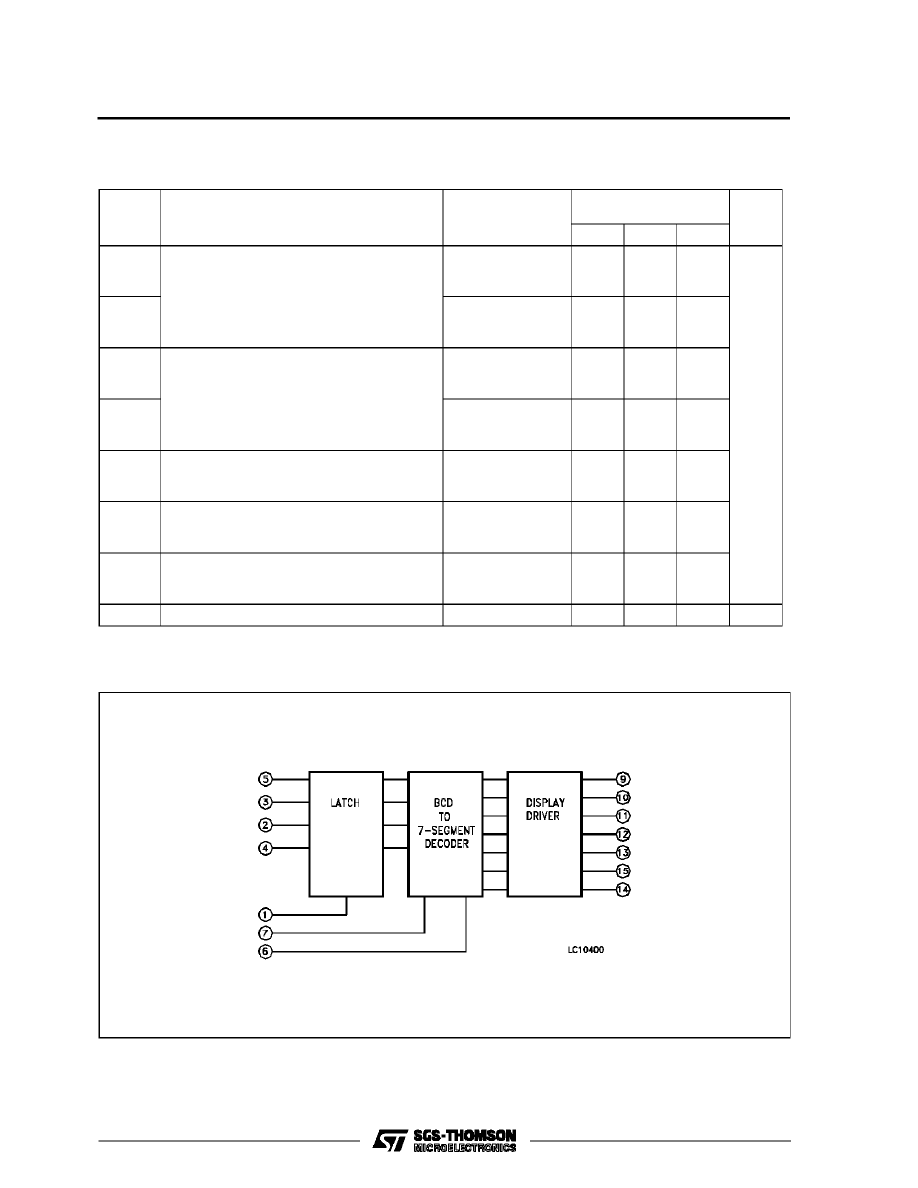
BCD-to-seven-segment latch/decoder/driver functional diagram
HCC/HCF4543B
5/12
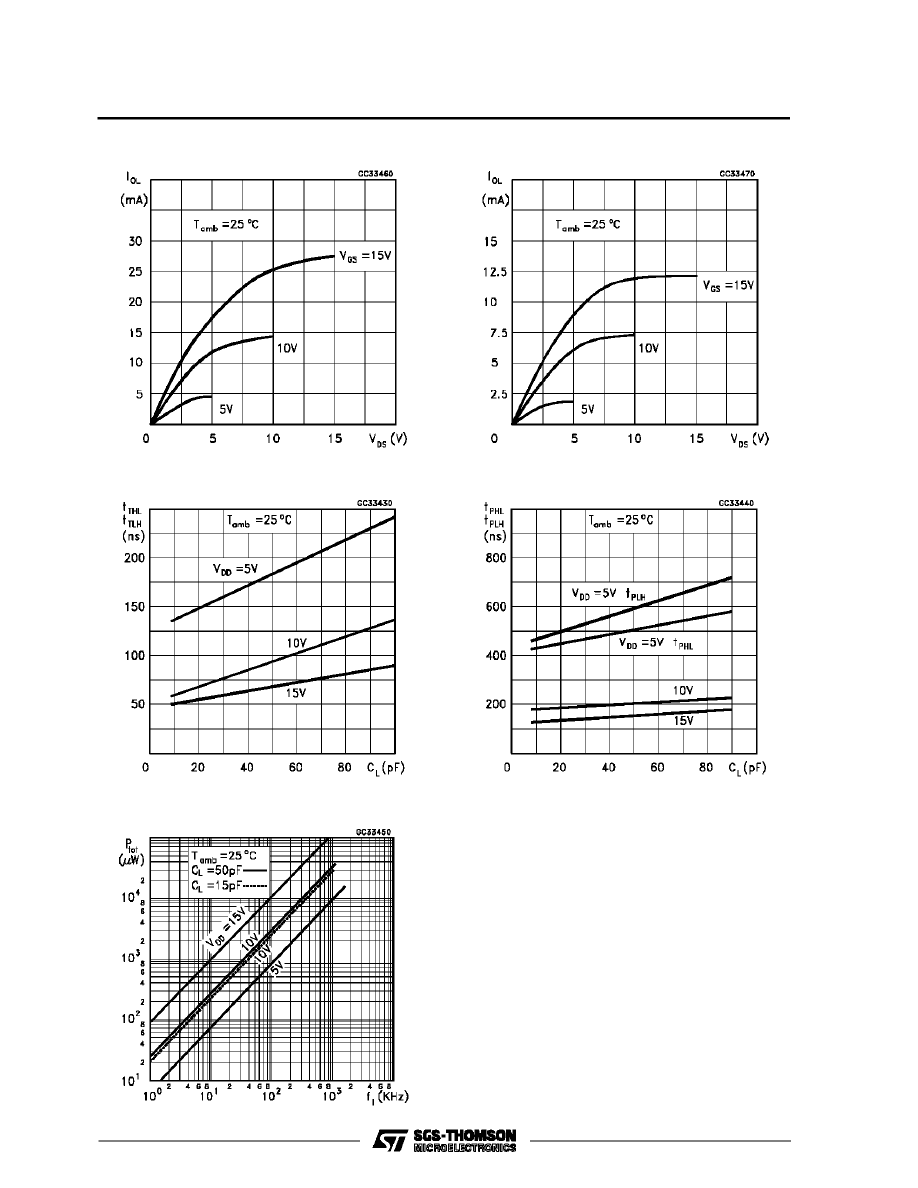
Typical Output Low (sink) Current Characteristics.
Minimum Output Low (sink) Current Characteristics.
Typical Transition Time as a Function of Load Ca-
pacitance
Typical Propagation Delay Time as a Function of
Load Capacitance
Typical Dinamic Power Dissipation as a Function of
Frequency
HCC/HCF4543B
6/12
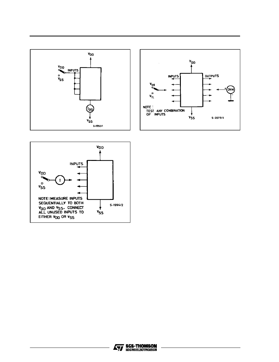
Input Voltage Test Circuit.
Quiescent Device Current Test Circuit.
Input-leakage -current Test Circuit.
HCC/HCF4543B
7/12
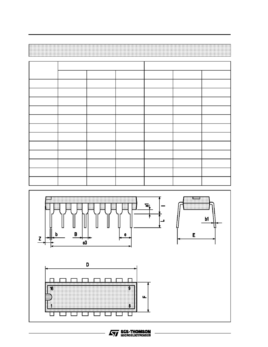
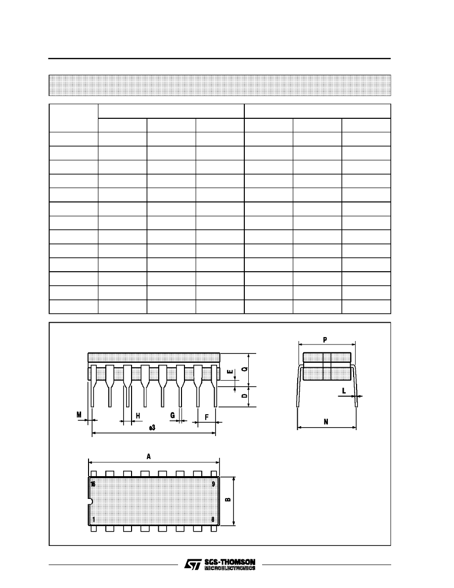
Plastic DIP16 (0.25) MECHANICAL DATA
DIM.
mm
inch
MIN.
TYP.
MAX.
MIN.
TYP.
MAX.
a1
0.51
0.020
B
0.77
1.65
0.030
0.065
b
0.5
0.020
b1
0.25
0.010
D
20
0.787
E
8.5
0.335
e
2.54
0.100
e3
17.78
0.700
F
7.1
0.280
I
5.1
0.201
L
3.3
0.130
Z
1.27
0.050
P001C
HCC/HCF4543B
8/12
Ceramic DIP16/1 MECHANICAL DATA
DIM.
mm
inch
MIN.
TYP.
MAX.
MIN.
TYP.
MAX.
A
20
0.787
B
7
0.276
D
3.3
0.130
E
0.38
0.015
e3
17.78
0.700
F
2.29
2.79
0.090
0.110
G
0.4
0.55
0.016
0.022
H
1.17
1.52
0.046
0.060
L
0.22
0.31
0.009
0.012
M
0.51
1.27
0.020
0.050
N
10.3
0.406
P
7.8
8.05
0.307
0.317
Q
5.08
0.200
P053D
HCC/HCF4543B
9/12
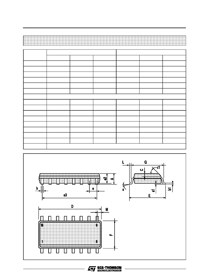
SO16 (Narrow) MECHANICAL DATA
DIM.
mm
inch
MIN.
TYP.
MAX.
MIN.
TYP.
MAX.
A
1.75
0.068
a1
0.1
0.2
0.004
0.007
a2
1.65
0.064
b
0.35
0.46
0.013
0.018
b1
0.19
0.25
0.007
0.010
C
0.5
0.019
c1
45
°
(typ.)
D
9.8
10
0.385
0.393
E
5.8
6.2
0.228
0.244
e
1.27
0.050
e3
8.89
0.350
F
3.8
4.0
0.149
0.157
G
4.6
5.3
0.181
0.208
L
0.5
1.27
0.019
0.050
M
0.62
0.024
S
8
°
(max.)
P013H
HCC/HCF4543B
10/12
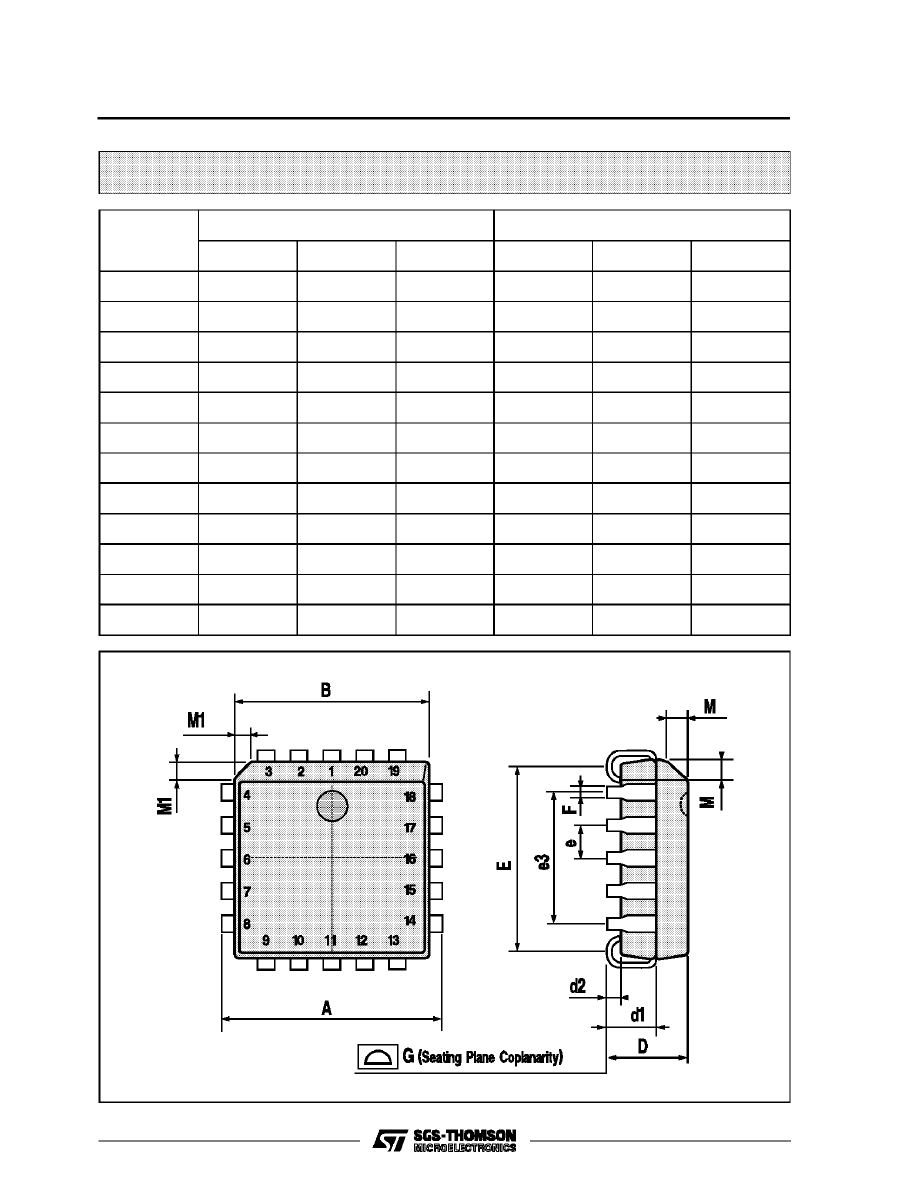
PLCC20 MECHANICAL DATA
DIM.
mm
inch
MIN.
TYP.
MAX.
MIN.
TYP.
MAX.
A
9.78
10.03
0.385
0.395
B
8.89
9.04
0.350
0.356
D
4.2
4.57
0.165
0.180
d1
2.54
0.100
d2
0.56
0.022
E
7.37
8.38
0.290
0.330
e
1.27
0.050
e3
5.08
0.200
F
0.38
0.015
G
0.101
0.004
M
1.27
0.050
M1
1.14
0.045
P027A
HCC/HCF4543B
11/12
Information furnished is believed to be accurate and reliable. However, SGS-THOMSON Microelectronics assumes no responsability for the
consequences of use of such information nor for any infringement of patents or other rights of third parties which may results from its use. No
license is granted by implication or otherwise under any patent or patent rights of SGS-THOMSON Microelectronics. Specifications mentioned
in this publication are subject to change without notice. This publication supersedes and replaces all information previously supplied.
SGS-THOMSON Microelectronics products are not authorized for use as critical components in life support devices or systems without express
written approval of SGS-THOMSON Microelectonics.
1994 SGS-THOMSON Microelectronics - All Rights Reserved
SGS-THOMSON Microelectronics GROUP OF COMPANIES
Australia - Brazil - France - Germany - Hong Kong - Italy - Japan - Korea - Malaysia - Malta - Morocco - The Netherlands -
Singapore - Spain - Sweden - Switzerland - Taiwan - Thailand - United Kingdom - U.S.A
HCC/HCF4543B
12/12
Wyszukiwarka
Podobne podstrony:
4543
4543
4543
praca-licencjacka-b7-4543, Dokumenty(8)
4543
4543
IMSLP41656 SIBLEY1802 4543 d45a 39087012466845benediction
więcej podobnych podstron