
Intel
®
Architecture
Optimization
Reference Manual
Copyright © 1998, 1999 Intel Corporation
All Rights Reserved
Issued in U.S.A.
Order Number: 245127-001


Intel
®
Architecture
Optimization
Reference Manual
Order Number: 730795-001
Revision
Revision History
Date
001
Documents Streaming SIMD Extensions optimization
techniques for Pentium
®
II
and Pentium III processors.
02/99

Information in this document is provided in connection with Intel products. No license, express or implied, by estoppel
or otherwise, to any intellectual property rights is granted by this document. Except as provided in Intel’s Terms and Con-
ditions of Sale for such products, Intel assumes no liability whatsoever, and Intel disclaims any express or implied war-
ranty, relating to sale and/or use of Intel products including liability or warranties relating to fitness for a particular
purpose, merchantability, or infringement of any patent, copyright or other intellectual property right. Intel products are
not intended for use in medical, life saving, or life sustaining applications.
This Intel® Architecture Optimization manual as well as the software described in it is furnished under license and may
only be used or copied in accordance with the terms of the license. The information in this manual is furnished for infor-
mational use only, is subject to change without notice, and should not be construed as a commitment by Intel Corpora-
tion. Intel Corporation assumes no responsibility or liability for any errors or inaccuracies that may appear in this
document or any software that may be provided in association with this document.
Except as permitted by such license, no part of this document may be reproduced, stored in a retrieval system, or trans-
mitted in any form or by any means without the express written consent of Intel Corporation.
Intel may make changes to specifications and product descriptions at any time, without notice.
* Third-party brands and names are the property of their respective owners.
Copyright © Intel Corporation 1998, 1999.

iii
Contents
Tuning Your Application ......................................................... xvii
About This Manual................................................................ xviii
Related Documentation .......................................................... xix
Notational Conventions............................................................ xx
Processor Architecture Overview
The Processors’ Execution Architecture................................ 1-1
®
II and Pentium III Processors Pipeline....... 1-2
The In-order Issue Front End ....................................... 1-2
The Out-of-order Core.................................................. 1-3
In-Order Retirement Unit .............................................. 1-3
Front-End Pipeline Detail .................................................. 1-4
Instruction Prefetcher ................................................... 1-4
Decoders ...................................................................... 1-4
Branch Prediction Overview ......................................... 1-5
Dynamic Prediction ...................................................... 1-6
Static Prediction ........................................................... 1-6
Execution Core Detail ....................................................... 1-7
Execution Units and Ports ............................................ 1-9
Caches of the Pentium II and Pentium III
Processors ............................................................... 1-10
Store Buffers .............................................................. 1-11

iv
Intel Architecture Optimization Reference Manual
Streaming SIMD Extensions of the Pentium III Processor... 1-12
Single-Instruction, Multiple-Data (SIMD)......................... 1-13
New Data Types .............................................................. 1-13
Streaming SIMD Extensions Registers ........................... 1-14
MMX™ Technology.............................................................. 1-15
General Optimization Guidelines
Integer Coding Guidelines ..................................................... 2-1
Branch Prediction .................................................................. 2-2
Dynamic Branch Prediction............................................... 2-2
Static Prediction ................................................................ 2-3
Eliminating and Reducing the Number of Branches ......... 2-5
Performance Tuning Tip for Branch Prediction.................. 2-8
Partial Register Stalls ............................................................ 2-8
Performance Tuning Tip for Partial Stalls ........................ 2-10
Alignment Rules and Guidelines.......................................... 2-11
Code ............................................................................... 2-11
Data ................................................................................ 2-12
Data Cache Unit (DCU) Split...................................... 2-12
Performance Tuning Tip for Misaligned Accesses...... 2-13
Instruction Scheduling ......................................................... 2-14
Scheduling Rules for Pentium II and Pentium III
Processors.................................................................... 2-14
Instruction Selection ............................................................ 2-16
The Use of lea Instruction ............................................... 2-17
Complex Instructions ...................................................... 2-17
Short Opcodes ................................................................ 2-17
8/16-bit Operands ........................................................... 2-18
Comparing Register Values ............................................ 2-19
Address Calculations ...................................................... 2-19

Contents
v
Clearing a Register......................................................... 2-19
Integer Divide ................................................................. 2-20
Comparing with Immediate Zero .................................... 2-20
Prolog Sequences .......................................................... 2-20
Epilog Sequences .......................................................... 2-20
Improving the Performance of Floating-point
Applications ...................................................................... 2-20
Guidelines for Optimizing Floating-point Code ............... 2-21
Improving Parallelism ..................................................... 2-21
Rules and Regulations of the fxch Instruction ................ 2-23
Memory Operands.......................................................... 2-24
Memory Access Stall Information................................... 2-24
Floating-point to Integer Conversion .............................. 2-25
Loop Unrolling ................................................................ 2-28
Floating-Point Stalls........................................................ 2-29
Hiding the One-Clock Latency of a
Floating-Point Store................................................. 2-29
Integer and Floating-point Multiply............................. 2-30
Floating-point Operations with Integer Operands ...... 2-30
FSTSW Instructions................................................... 2-31
Transcendental Functions .......................................... 2-31
Checking for Processor Support of Streaming SIMD
Extensions and MMX Technology....................................... 3-2
Checking for MMX Technology Support ........................... 3-2
Checking for Streaming SIMD Extensions Support.......... 3-3
Considerations for Code Conversion to SIMD
Programming ...................................................................... 3-4
Identifying Hotspots .......................................................... 3-6
Determine If Code Benefits by Conversion to
Streaming SIMD Extensions .......................................... 3-7
Coding Techniques................................................................ 3-7

vi
Intel Architecture Optimization Reference Manual
Coding Methodologies ...................................................... 3-8
Assembly.................................................................... 3-10
Intrinsics ..................................................................... 3-11
Classes ...................................................................... 3-12
Automatic Vectorization .............................................. 3-13
Stack and Data Alignment ................................................... 3-15
Alignment of Data Access Patterns ................................ 3-15
Stack Alignment For Streaming SIMD Extensions .......... 3-16
Data Alignment for MMX Technology .............................. 3-17
Data Alignment for Streaming SIMD Extensions ............ 3-18
Compiler-Supported Alignment .................................. 3-18
Improving Memory Utilization .............................................. 3-20
Data Structure Layout ..................................................... 3-21
Strip Mining ..................................................................... 3-23
Loop Blocking ................................................................. 3-25
Tuning the Final Application ............................................ 3-28
Using SIMD Integer Instructions
General Rules on SIMD Integer Code ................................... 4-1
Planning Considerations........................................................ 4-2
CPUID Usage for Detection of Pentium III Processor
SIMD Integer Instructions.................................................... 4-2
Using SIMD Integer, Floating-Point, and MMX Technology
Instructions .......................................................................... 4-2
Using the EMMS Instruction ............................................. 4-3
Guidelines for Using EMMS Instruction ............................ 4-5
SIMD Instruction Port Assignments .................................. 4-7
Coding Techniques for MMX Technology SIMD Integer
Instructions .......................................................................... 4-7
Unsigned Unpack.............................................................. 4-8
Signed Unpack.................................................................. 4-8

Contents
vii
Interleaved Pack without Saturation ............................... 4-11
Non-Interleaved Unpack ................................................. 4-12
Complex Multiply by a Constant ..................................... 4-14
Absolute Difference of Unsigned Numbers .................... 4-14
Absolute Difference of Signed Numbers ........................ 4-15
Absolute Value................................................................ 4-17
Clipping to an Arbitrary Signed Range [high, low] .......... 4-17
Clipping to an Arbitrary Unsigned Range [high, low] ...... 4-19
Generating Constants..................................................... 4-20
Coding Techniques for Integer Streaming SIMD
Extensions ........................................................................ 4-21
Extract Word ................................................................... 4-22
Insert Word ..................................................................... 4-22
Packed Signed Integer Word Maximum ......................... 4-23
Packed Unsigned Integer Byte Maximum....................... 4-23
Packed Signed Integer Word Minimum .......................... 4-23
Packed Unsigned Integer Byte Minimum........................ 4-24
Move Byte Mask to Integer ............................................. 4-24
Packed Multiply High Unsigned ...................................... 4-25
Packed Shuffle Word ...................................................... 4-25
Packed Sum of Absolute Differences ............................. 4-26
Packed Average (Byte/Word).......................................... 4-27
Memory Optimizations ........................................................ 4-27
Partial Memory Accesses............................................... 4-28
Instruction Selection to Reduce Memory Access Hits.... 4-30
Increasing Bandwidth of Memory Fills and Video Fills ... 4-32
Increasing Memory Bandwidth Using the MOVQ
Instruction................................................................ 4-32
Increasing Memory Bandwidth by Loading and
Storing to and from the Same DRAM Page............. 4-32
Increasing the Memory Fill Bandwidth by Using
Aligned Stores ......................................................... 4-33

viii
Intel Architecture Optimization Reference Manual
Use 64-Bit Stores to Increase the Bandwidth
to Video.................................................................... 4-33
Increase the Bandwidth to Video Using Aligned
Stores....................................................................... 4-33
Scheduling for the SIMD Integer Instructions ...................... 4-34
Scheduling Rules ............................................................ 4-34
Optimizing Floating-point Applications
Rules and Suggestions.......................................................... 5-1
Planning Considerations........................................................ 5-2
Which Part of the Code Benefits from SIMD
Floating-point Instructions? ............................................ 5-3
MMX Technology and Streaming SIMD Extensions
Floating-point Code ....................................................... 5-3
Scalar Code Optimization ................................................. 5-3
EMMS Instruction Usage Guidelines ................................ 5-4
CPUID Usage for Detection of SIMD Floating-point
Support ........................................................................... 5-5
Data Alignment ................................................................. 5-5
Data Arrangement............................................................. 5-6
Vertical versus Horizontal Computation ....................... 5-6
Data Swizzling............................................................ 5-10
Data Deswizzling........................................................ 5-13
Using MMX Technology Code for Copy or Shuffling
Functions ................................................................. 5-17
Horizontal ADD .......................................................... 5-18
Scheduling ..................................................................... 5-22
Scheduling with the Triple-Quadruple Rule..................... 5-24
Modulo Scheduling (or Software Pipelining) ................... 5-25
Scheduling to Avoid Register Allocation Stalls................ 5-31
Forwarding from Stores to Loads.................................... 5-31
Conditional Moves and Port Balancing ................................ 5-31
Conditional Moves........................................................... 5-31

Contents
ix
Port Balancing ................................................................ 5-33
Streaming SIMD Extension Numeric Exceptions ................ 5-36
Exception Priority ........................................................... 5-37
Automatic Masked Exception Handling .......................... 5-38
Software Exception Handling - Unmasked Exceptions .. 5-39
Interaction with x87 Numeric Exceptions ....................... 5-41
CVTTPS2PI
/
CVTTSS2SI
Instructions ................. 5-42
Flush-to-Zero Mode ........................................................ 5-42
Optimizing Cache Utilization for Pentium III Processors
Prefetch and Cacheability Instructions .................................. 6-2
The Prefetching Concept.................................................. 6-2
The Prefetch Instructions.................................................. 6-3
Prefetch and Load Instructions......................................... 6-4
The Non-temporal Store Instructions ............................... 6-5
The sfence Instruction ...................................................... 6-6
Streaming Non-temporal Stores ....................................... 6-6
Other Cacheability Control Instructions ............................ 6-9
Memory Optimization Using Prefetch.................................. 6-10
Prefetching Usage Checklist .......................................... 6-12
Prefetch Scheduling Distance ........................................ 6-12
Prefetch Concatenation .................................................. 6-13
Minimize Number of Prefetches ..................................... 6-15
Mix Prefetch with Computation Instructions ................... 6-16
Prefetch and Cache Blocking Techniques ...................... 6-18
Single-pass versus Multi-pass Execution ....................... 6-23
Memory Bank Conflicts .................................................. 6-25
Non-temporal Stores and Software Write-Combining .... 6-25
Cache Management ....................................................... 6-26
Video Encoder ........................................................... 6-27

x
Intel Architecture Optimization Reference Manual
Video Decoder ........................................................... 6-27
Conclusions from Video Encoder and Decoder
Implementation ........................................................ 6-28
Using Prefetch and Streaming-store for a
Simple Memory Copy............................................... 6-28
VTune™ Performance Analyzer............................................. 7-2
Using Sampling Analysis for Optimization ........................ 7-2
Time-based Sampling .................................................. 7-2
Event-based Sampling ................................................. 7-4
Sampling Performance Counter Events ....................... 7-4
Call Graph Profiling ........................................................... 7-7
Call Graph Window ...................................................... 7-7
Static Code Analysis ......................................................... 7-9
Static Assembly Analysis ........................................... 7-10
Dynamic Assembly Analysis ...................................... 7-10
Code Coach Optimizations......................................... 7-11
Assembly Coach Optimization Techniques ................ 7-13
Intel Compiler Plug-in .......................................................... 7-14
Code Optimization Options ........................................ 7-14
Interprocedural and Profile-Guided Optimizations ..... 7-17
Intel Performance Library Suite ........................................... 7-18
Benefits Summary........................................................... 7-19
Libraries Architecture ..................................................... 7-19
Optimizations with Performance Library Suite ................ 7-20
Register Viewing Tool (RVT) ................................................ 7-21

Contents
xi
Appendix A Optimization of Some Key Algorithms for the
Newton-Raphson Method with the Reciprocal Instructions... A-2
Performance Improvements ............................................. A-3
Newton-Raphson Method for Reciprocal Square Root .... A-3
Newton-Raphson Inverse Reciprocal Approximation ....... A-5
3D Transformation Algorithms ............................................... A-7
SoA .............................................................................. A-8
Prefetching................................................................... A-9
Avoiding Dependency Chains ...................................... A-9
Implementation ................................................................. A-9
Assembly Code for SoA Transformation......................... A-13
Motion Estimation................................................................ A-14
Performance Improvements ........................................... A-14
Implementation ............................................................... A-15
Upsample ............................................................................ A-15
Upsampling Algorithm .................................................. A-16
FIR Filter Algorithm Using Streaming SIMD Extensions ..... A-17
Performance Improvements for Real FIR Filter .............. A-17
Parallel Multiplication and Interleaved Additions........ A-17
Reducing Data Dependency and Register Pressure . A-17
Scheduling for the Reorder Buffer and the
Reservation Station ................................................. A-18
Wrapping the Loop Around (Software Pipelining)...... A-18
Advancing Memory Loads ......................................... A-19
Separating Memory Accesses from Operations ........ A-19

xii
Intel Architecture Optimization Reference Manual
Unrolling the Loop ...................................................... A-19
Minimizing Pointer Arithmetic/Eliminating
Unnecessary Micro-ops ........................................... A-20
Performance Improvements for the Complex FIR Filter .. A-21
Code Samples ................................................................ A-22
Appendix B Performance-Monitoring Events and Counters
Performance-affecting Events................................................ B-1
Instruction Specification ............................................. B-13
Appendix C Instruction to Decoder Specification
Appendix D Streaming SIMD Extensions Throughput and Latency
Appendix E Stack Alignment for Streaming SIMD Extensions
Stack Frames......................................................................... E-1
Aligned esp-Based Stack Frames ..................................... E-4
Aligned ebp-Based Stack Frames..................................... E-6
Stack Frame Optimizations ............................................... E-9
Inlined Assembly and ebx ...................................................... E-9
Appendix F The Mathematics of Prefetch Scheduling Distance
Simplified Equation ................................................................ F-1
Mathematical Model for PSD ................................................. F-2
No Preloading or Prefetch................................................. F-5
Compute Bound (Case:Tc >= T
l
+ T
b
) .............................. F-7

Contents
xiii
Compute Bound (Case: Tl + Tb > Tc > Tb) ...................... F-8
Memory Throughput Bound (Case: Tb >= Tc) ................. F-9
Example ......................................................................... F-10
Examples
2-1
Prediction Algorithm ..................................................... 2-4
2-2
Misprediction Example ................................................. 2-5
2-3
Assembly Equivalent of Conditional C Statement ........ 2-6
2-4
Code Optimization to Eliminate Branches .................... 2-6
2-5
Eliminating Branch with CMOV Instruction ................... 2-7
2-6
Partial Register Stall ..................................................... 2-9
2-7
Partial Register Stall with Pentium II and Pentium III
Processors ................................................................... 2-9
2-8
Simplifying the Blending of Code in Pentium II and
Pentium III Processors .............................................. 2-10
2-9
Scheduling Instructions for the Decoder ..................... 2-15
2-10 Scheduling Floating-Point Instructions ....................... 2-22
2-11 Coding for a Floating-Point Register File .................... 2-22
2-12 Using the FXCH Instruction ........................................ 2-23
2-13 Large and Small Load Stalls ...................................... 2-25
2-14 Algorithm to Avoid Changing the Rounding Mode ...... 2-26
2-15 Loop Unrolling ............................................................ 2-28
2-16 Hiding One-Clock Latency .......................................... 2-29
3-1
Identification of MMX Technology with cpuid ................ 3-2
3-2
Identification of Streaming SIMD Extensions with
cpuid 3-3
3-3
Identification of Streaming SIMD Extensions by
the OS .......................................................................... 3-4
3-4
Simple Four-Iteration Loop ........................................... 3-9
3-5
Streaming SIMD Extensions Using Inlined Assembly
Encoding .................................................................... 3-10
3-6
Simple Four-Iteration Loop Coded with Intrinsics ....... 3-11
3-7
C++ Code Using the Vector Classes .......................... 3-13

xiv
Intel Architecture Optimization Reference Manual
3-8
Automatic Vectorization for a Simple Loop ................. 3-14
3-9
C Algorithm for 64-bit Data Alignment ........................ 3-17
3-10 AoS data structure ...................................................... 3-22
3-11 SoA data structure ..................................................... 3-22
3-12 Pseudo-code Before Strip Mining ............................... 3-24
3-13 A Strip Mining Code .................................................... 3-25
3-14 Loop Blocking ............................................................. 3-26
4-1
Resetting the Register between __m64 and FP
Data Types .................................................................... 4-5
4-2
Unsigned Unpack Instructions ...................................... 4-8
4-3
Signed Unpack Instructions .......................................... 4-9
4-4
Interleaved Pack with Saturation ................................. 4-11
4-5
Interleaved Pack without Saturation ............................ 4-12
4-6
Unpacking Two Packed-word Sources in a
Non-interleaved Way ................................................... 4-13
4-7
Complex Multiply by a Constant .................................. 4-14
4-8
Absolute Difference of Two Unsigned Numbers .......... 4-15
4-9
Absolute Difference of Signed Numbers ..................... 4-16
4-10 Computing Absolute Value .......................................... 4-17
4-11 Clipping to an Arbitrary Signed Range [high, low] ...... 4-18
4-12 Simplified Clipping to an Arbitrary Signed Range ....... 4-19
4-13 Clipping to an Arbitrary Unsigned Range [high, low] .. 4-20
4-14 Generating Constants ................................................. 4-20
4-15 pextrw Instruction Code .............................................. 4-22
4-16 pinsrw Instruction Code .............................................. 4-23
4-17 pmovmskb Instruction Code ....................................... 4-24
4-18 pshuf Instruction Code ................................................ 4-26
4-19 A Large Load after a Series of Small Stalls ................ 4-28
4-20 Accessing Data without Delay ..................................... 4-29
4-21 A Series of Small Loads after a Large Store ............... 4-29
4-22 Eliminating Delay for a Series of Small Loads after
a Large Store .............................................................. 4-30
5-1
Pseudocode for Horizontal (xyz, AoS) Computation ..... 5-9

Contents
xv
5-2
Pseudocode for Vertical (xxxx, yyyy, zzzz, SoA)
Computation ................................................................. 5-9
5-3
Swizzling Data ............................................................ 5-10
5-4
Swizzling Data Using Intrinsics .................................. 5-12
5-5
Deswizzling Data ........................................................ 5-14
5-6
Deswizzling Data Using the movlhps and
shuffle Instructions ..................................................... 5-15
5-7
Deswizzling Data Using Intrinsics with the movlhps
and shuffle Instructions .............................................. 5-16
5-8
Using MMX Technology Code for Copying or
Shuffling ..................................................................... 5-18
5-9
Horizontal Add Using movhlps/movlhps ..................... 5-20
5-10 Horizontal Add Using Intrinsics with
movhlps/movlhps 5-21
5-11 Scheduling Instructions that Use the Same Register . 5-22
5-12 Scheduling with the Triple/Quadruple Rule ................ 5-25
5-13 Proper Scheduling for Performance Increase ............. 5-29
5-14 Scheduling with Emulated Conditional Branch ........... 5-32
5-15 Replacing the Streaming SIMD Extensions Code
with the MMX Technology Code ................................. 5-34
5-16 Typical Dot Product Implementation ........................... 5-35
6-1
Prefetch Scheduling Distance .................................... 6-13
6-2
Using Prefetch Concatenation .................................... 6-14
6-3
Concatenation and Unrolling the Last Iteration of
Inner Loop .................................................................. 6-15
6-4
Prefetch and Loop Unrolling ....................................... 6-16
6-5
Spread Prefetch Instructions ...................................... 6-17
6-6
Data Access of a 3D Geometry Engine without
Strip-mining ................................................................ 6-21
6-7
Data Access of a 3D Geometry Engine with
Strip-mining ................................................................ 6-22
6-8
Basic Algorithm of a Simple Memory Copy ................ 6-28
6-9
An Optimized 8-byte Memory Copy ............................ 6-30

xvi
Intel Architecture Optimization Reference Manual
A-1 Newton-Raphson Method for Reciprocal Square Root
Approximation ...............................................................A-4
A-2 Newton-Raphson Inverse Reciprocal Approximation ....A-5
A-3 Transform SoA Functions, C Code ..............................A-10
E-1 Aligned esp-Based Stack Frames ................................E-5
E-2 Aligned ebp-based Stack Frames ................................E-6
F-1
Calculating Insertion for Scheduling Distance of 3 ......F-3
Figures
1-1
The Complete Pentium II and Pentium III
Processors Architecture ................................................ 1-2
1-2
TExecution Units and Ports in the Out-Of-Order
Core 1-10
1-3
TStreaming SIMD Extensions Data Type .................... 1-14
1-4
TStreaming SIMD Extensions Register Set ................ 1-14
1-5
TMMX Technology 64-bit Data Type ........................... 1-15
1-6
TMMX Technology Register Set .................................. 1-16
2-1
TPentium II Processor Static Branch Prediction
Algorithm ....................................................................... 2-4
2-2
DCU Split in the Data Cache ...................................... 2-13
3-1
Converting to Streaming SIMD Extensions Chart ......... 3-5
3-2
Hand-Coded Assembly and High-Level Compiler
Performance Tradeoffs .................................................. 3-9
3-3
Loop Blocking Access Pattern .................................... 3-27
4-1
Using EMMS to Reset the Tag after an
MMX Instruction ............................................................ 4-4
4-2
PACKSSDW mm, mm/mm64 Instruction Example ..... 4-10
4-3
Interleaved Pack with Saturation ................................. 4-10
4-4
Result of Non-Interleaved Unpack in MM0 ................. 4-12
4-5
Result of Non-Interleaved Unpack in MM1 ................. 4-13
4-6
pextrw Instruction ........................................................ 4-22
4-7
pinsrw Instruction ........................................................ 4-23
4-8
pmovmskb Instruction Example .................................. 4-24

Contents
xvii
4-9
pshuf Instruction Example .......................................... 4-25
4-10 PSADBW Instruction Example ................................... 4-26
5-1
Dot Product Operation .................................................. 5-8
5-2
Horizontal Add Using movhlps/movlhps ..................... 5-19
5-3
Modulo Scheduling Dependency Graph ..................... 5-26
6-1
Memory Access Latency and Execution Without
Prefetch ...................................................................... 6-11
6-2
Memory Access Latency and Execution With
Prefetch ...................................................................... 6-11
6-3
Cache Blocking - Temporally Adjacent and
Non-adjacent Passes ................................................. 6-19
6-4
Examples of Prefetch and Strip-mining for Temporally
Adjacent and Non-adjacent Passes Loops ................. 6-20
6-5
Benefits of Incorporating Prefetch into Code .............. 6-23
6-6
Single-Pass vs. Multi-Pass 3D Geometry Engines ..... 6-24
7-1
Sampling Analysis of Hotspots by Location .................. 7-3
7-2
Processor Events List ................................................... 7-5
7-3
Call Graph Window ....................................................... 7-8
7-4
Code Coach Optimization Advice ............................... 7-12
7-5
The RVT: Registers and Disassembly Window .......... 7-22
E-1 Stack Frames Based on Alignment Type ...................... E-3
F-1
Pentium II and Pentium III Processors Memory
Pipeline Sketch ............................................................. F-4
F-2
Execution Pipeline, No Preloading or Prefetch ............. F-6
F-3
Compute Bound Execution Pipeline ............................. F-7
F-4
Compute Bound Execution Pipeline ............................. F-8
F-5
Memory Throughput Bound Pipeline ............................ F-9
F-6
Accesses per Iteration, Example 1 ............................. F-11
F-7
Accesses per Iteration, Example 2 ............................. F-12
Tables
1-1
Pentium II and Pentium III Processors Execution
Units ............................................................................. 1-8

xviii
Intel Architecture Optimization Reference Manual
4-1
Port Assignments .......................................................... 4-7
5-1
EMMS Instruction Usage Guidelines ............................ 5-4
5-2
SoA Form of Representing Vertices Data ..................... 5-7
5-3
EMMS Modulo Scheduling .......................................... 5-27
5-4
EMMS Schedule – Overlapping Iterations .................. 5-27
5-5
Modulo Scheduling with Interval MRT (II=4) ............... 5-28
B-1 Performance Monitoring Events ....................................B-2
C-1 Pentium II and Pentium III Processors Instruction
to Decoder Specification .............................................. C-1
C-2 MMX Technology Instruction to Decoder
Specification ............................................................... C-17
D-1 Streaming SIMD Extensions Throughput
and Latency ................................................................. D-1

xvii
Introduction
Developing high-performance applications for Intel
®
architecture
(IA)-based processors can be more efficient with better understanding of the
newest IA. Even though the applications developed for the 8086/8088,
80286, Intel386™ (DX or SX), and Intel486™ processors will execute on
the Pentium
®
, Pentium Pro, Pentium II and Pentium
III
processors without
any modification or recomputing, the code optimization techniques
combined with the advantages of the newest processors can help you tune
your application to its greatest potential. This manual provides information
on Intel architecture as well as describes code optimization techniques to
enable you to tune your application for best results, specifically when run on
Pentium II and Pentium
III
processors.
Tuning Your Application
Tuning an application to high performance across Intel architecture-based
processors requires background information about the following:
•
the Intel architecture.
•
critical stall situations that may impact the performance of your
application and other performance setbacks within your application
•
your compiler optimization capabilities
•
monitoring the application’s performance
To help you understand your application and where to begin tuning, you can
use Intel’s VTune™ Performance Analyzer. This tool helps you see the
performance event counters data of your code provided by the Pentium II
and Pentium
III
processors. This manual informs you about appropriate

xviii
Intel Architecture Optimization Reference Manual
performance counter for measurement. For VTune Performance Analyzer
order information, see its web home page at
http://developer.intel.com/vtune.
About This Manual
This manual assumes that you are familiar with IA basics, as well as with C
or C++ and assembly language programming. The manual consists of the
following parts:
Introduction. Defines the purpose and outlines the contents of this manual.
Chapter 1—Processor Architecture Overview. Overviews the
architectures of the Pentium II and Pentium
III
processors.
Chapter 2—General Optimization Guidelines. Describes the code
development techniques to utilize the architecture of Pentium II and
Pentium
III
processors as well as general strategies of efficient memory
utilization.
Chapter 3—Coding for SIMD Architectures. Describes the following
coding methodologies: assembly, inlined-assembly, intrinsics, vector
classes, auto-vectorization, and libraries. Also discusses strategies for
altering data layout and restructuring algorithms for SIMD-style coding.
Chapter 4—Using SIMD Integer Instructions. Describes optimization
rules and techniques for high-performance integer and MMX™ technology
applications.
Chapter 5—Optimizing Floating-Point Applications. Describes rules
and optimization techniques, and provides code examples specific to
floating-point code, including SIMD-floating point code for Streaming
SIMD Extensions.
Chapter 6—Optimizing Cache Utilization for Pentium
III
Processors.
Describes the memory hierarchy of Pentium II and Pentium
III
processor
architectures, and how to best use it. The
prefetch
instruction and cache
control management instructions for Streaming SIMD Extensions are also
described.

Introduction
xix
Chapter 7— Application Performance Tools. Describes application
performance tools: VTune analyzer, Intel® Compiler plug-ins, and Intel®
Performance Libraries Suite. For each tool, techniques and code optimization
strategies that help you to take advantage of the Intel architecture are described.
Appendix A—Optimization of Some Key Algorithms for the Pentium II
and Pentium
III
Processors. Describes how to optimize the following common
algorithms using the Streaming SIMD Extensions: 3D lighting and transform,
image compression, audio decomposition, and others.
Appendix B—Performance Monitoring Events and Counters. Describes
performance-monitoring events and counters and their functions.
Appendix C—Instruction to Decoder Specification. Summarizes the IA
macro instructions with Pentium II and Pentium
III
processor decoding
information to enable scheduling
.
Appendix D—Streaming SIMD Extensions Throughput and Latency.
Summarizes in a table the instructions’ throughput and latency characteristics.
Appendix E—Stack Alignment for Streaming SIMD Extensions. Details on
the alignment of the stacks of data for Streaming SIMD Extensions.
Appendix F—The Mathematics of Prefetch Scheduling Distance. Discusses
how far away prefetch instructions should be inserted.
Related Documentation
For more information on the Intel architecture, specific techniques and
processor architecture terminology referenced in this manual, see the following
documentation:
Intel Architecture MMX™ Technology Programmer's Reference Manual, order
number 243007
Pentium Processor Family Developer’s Manual, Volumes 1, 2, and 3, order
numbers 241428, 241429, and 241430
Pentium Pro Processor Family Developer’s Manual, Volumes 1, 2, and 3, order
numbers 242690, 242691, and 242692
Pentium II Processor Developer’s Manual, order number 243502
Intel C/C++ Compiler for Win32* Systems User’s Guide, order number
718195

xx
Intel Architecture Optimization Reference Manual
Notational Conventions
This manual uses the following conventions:
This type style
Indicates an element of syntax, a reserved word, a
keyword, a filename, instruction, computer
output, or part of a program example. The text
appears in lowercase unless uppercase is
significant.
THIS TYPE STYLE
Indicates a value, for example,
TRUE
,
CONST1
, or
a variable, for example,
A
,
B
, or register names
MMO
through
MM7
.
l
indicates lowercase letter L in examples.
1
is the
number 1 in examples.
O
is the uppercase O in
examples.
0
is the number 0 in examples.
This type style
Indicates a placeholder for an identifier, an
expression, a string, a symbol, or a value.
Substitute one of these items for the placeholder.
...
(ellipses)
Indicate that a few lines of the code are omitted.
This type style
Indicates a hypertext link.

1-1
Processor Architecture
Overview
1
This chapter provides an overview of the architectural features of the
Pentium
®
II and Pentium
III
processors and explains the new capabilities of
the Pentium
III
processor. The Streaming SIMD Extensions of the Pentium
III
processor introduce new general purpose integer and floating-point
SIMD instructions, which accelerate applications performance over the
Pentium II processors.
The Processors’ Execution Architecture
The Pentium II and Pentium
III
processors are aggressive microarchitectural
implementations of the 32-bit Intel
®
architecture (IA). They are designed
with a dynamic execution architecture that provides the following features:
•
out-of-order speculative execution to expose parallelism
•
superscalar issue to exploit parallelism
•
hardware register renaming to avoid register name space limitations
•
pipelined execution to enable high clock speeds
•
branch prediction to avoid pipeline delays
The microarchitecture is designed to execute legacy 32-bit Intel architecture
code as quickly as possible, without additional effort from the programmer.
This optimization manual assists the developer in leveraging the features of
the microarchitecture to attain greater performance by understanding and
working with these features to maximally enhance performance.
1-2
1
Intel Architecture Optimization Reference Manual
The Pentium
®
II
and Pentium III Processors Pipeline
The Pentium II and Pentium
III
processors’ pipelines contain three parts:
•
the in-order issue front end
•
the out-of-order core
•
the in-order retirement unit.
Figure 1-1 gives an overview of the Pentium II and Pentium
III
processors
architecture.
The In-order Issue Front End
The front end supplies instructions in program order to the out-of-order
core. It fetches and decodes Intel architecture-based processor
macroinstructions, and breaks them down into simple operations called
micro-ops (µops). It can issue multiple µops per cycle, in original program
order, to the out-of-order core. Since the core aggressively reorders and
executes instructions out of program order, the most important
consideration in performance tuning is to ensure that enough µops are ready
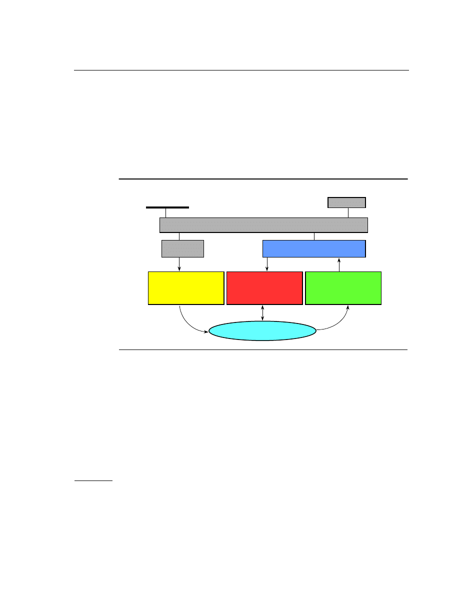
Figure 1-1
The Complete Pentium
II
and Pentium III Processors Architecture
Fetch & Decode Unit
(In order unit)
•Fetches instructions
•Decodes instructions to µOPs
•Performs branch prediction
Retirement Unit
(In order unit)
•Retires instructions in order
•Writes results to registers/memory
Dispatch / Execute Unit
(out of order unit)
•Schedules and executes µOPs
•Contains 5 execution ports
L2 cache
Bus Interface Unit
L1 data cache
L1 instruction
cache
Instruction Pool/reorder buffer
•Buffer of µOPs waiting for execution
System bus
Fetch
Load
Store

Processor Architecture Overview
1
1-3
for execution. Accurate branch prediction, instruction prefetch, and fast
decoding are essential to getting the most performance out of the in-order
front end.
The Out-of-order Core
The core’s ability to execute instructions out of order is a key factor in
exploiting parallelism. This feature enables the processor to reorder
instructions so that if one µop is delayed while waiting for data or a
contended resource, other µops that are later in program order may proceed
around it. The processor employs several buffers to smooth the flow of
µops. This implies that when one portion of the pipeline experiences a
delay, that delay may be covered by other operations executed in parallel or
by executing µops which were previously queued up in a buffer. The delays
described in this chapter are treated in this manner.
The out-of-order core buffers µops in a Reservation Station (RS) until their
operands are ready and resources are available. Each cycle, the core may
dispatch up to five µops, as explained in more detail later in the chapter.
The core is designed to facilitate parallel execution. Load and store
instructions may be issued simultaneously. Most simple operations, such as
integer operations, floating-point add, and floating-point multiply, can be
pipelined with a throughput of one or two operations per clock cycle. Long
latency operations can proceed in parallel with short latency operations.
In-Order Retirement Unit
For semantically-correct execution, the results of instructions must be
processed in original program order. Likewise, any exceptions that occur
must be processed in program order. When a µop completes and writes its
result, it is retired. Up to three µops may be retired per cycle. The unit in the
processor which buffers completed µops is the reorder buffer (ROB). ROB
updates the architectural state in order, that is, updates the state of
instructions and registers in the program semantics order. ROB also
manages the ordering of exceptions.

1-4
1
Intel Architecture Optimization Reference Manual
Front-End Pipeline Detail
For better understanding operation of the Pentium II and Pentium
III
processors, this section explains the main processing units of their front-end
pipelines: instruction prefetcher, decoders, and branch prediction.
Instruction Prefetcher
The instruction prefetcher performs aggressive prefetch of straight line
code. The Pentium II and Pentium
III
processors read in instructions from
16-byte-aligned boundaries. For example, if the modulo 16 branch target
address (the address of a label) is equal to 14, only two useful instruction
bytes are fetched in the first cycle. The rest of the instruction bytes are
fetched in subsequent cycles.
Decoders
Pentium II and Pentium
III
processors have three decoders. In each clock
cycle, the first decoder is capable of decoding one macroinstruction made
up of four or fewer µops. It can handle any number of bytes up to the
maximum of 15, but nine- or more-byte instructions require additional
cycles. In each clock cycle, the other two decoders can each decode an
instruction of one µop, and up to eight bytes. Instructions composed of more
than four µops take multiple cycles to decode.
Simple instructions have one to four µops; complex instructions (for
example,
cmpxcg
) generally have more than four µops. Complex
instructions require multiple cycles to decode.
During every clock cycle, up to three macroinstructions are decoded.
However, if the instructions are complex or are over seven bytes long, the
decoder is limited to decoding fewer instructions. The decoders can decode:
•
up to three macroinstructions per clock cycle
•
up to six µops per clock cycle
NOTE.
Instruction fetch is always intended for an aligned 16-byte
block.

Processor Architecture Overview
1
1-5
When programming in assembly language, try to schedule your instructions
in a 4-1-1 µop sequence, which means instruction with four µops followed
by two instructions each with one µop. Scheduling the instructions in a
4-1-1 µop sequence increases the number of instructions that can be
decoded during one clock cycle.
Most commonly used instructions have the following µop numbers:
•
Simple instructions of the register-register form have only one µop.
•
Load instructions are only one µop.
•
Store instructions have two µops.
•
Simple read-modify instructions are two µops.
•
Simple instructions of the register-memory form have two to three
µops.
•
Simple read-modify-write instructions have four µops.
See Appendix C, “
Instruction to Decoder Specification
” for a table
specifying the number of µops required by each instruction in the Intel
architecture instruction set.
Branch Prediction Overview
Pentium II and Pentium
III
processors use a branch target buffer (BTB) to
predict the direction and target of branches based on an instruction’s
address. The address of the branch instruction is available before the branch
has been decoded, so a BTB-based prediction can be made as early as
possible to avoid delays caused by going the wrong direction on a branch.
The 512-entry BTB stores the history of previously-seen branches and their
targets. When a branch is prefetched, the BTB feeds the target address
directly into the instruction fetch unit (IFU). Once the branch is executed,
the BTB is updated with the target address. Using the branch target buffer
allows dynamic prediction of previously seen branches.
Once the branch instruction is decoded, the direction of the branch (forward
or backward) is known. If there was not a valid entry in the BTB for the
branch, the static predictor makes a prediction based on the direction of the
branch.

1-6
1
Intel Architecture Optimization Reference Manual
Dynamic Prediction
The branch target buffer prediction algorithm includes pattern matching and
can track up to the last four branch directions per branch address. For
example, a loop with four or fewer iterations should have about 100%
correct prediction.
Additionally, Pentium II and Pentium
III
processors have a return stack
buffer (RSB) that can predict return addresses for procedures that are called
from different locations in succession. This increases the benefit of
unrolling loops containing function calls. It also mitigates the need to put
certain procedures in-line since the return penalty portion of the procedure
call overhead is reduced.
Pentium II and Pentium
III
processors have three levels of branch support
that can be quantified in the number of cycles lost:
1.
Branches that are not taken suffer no penalty. This applies to those
branches that are correctly predicted as not taken by the BTB, and to
forward branches that are not in the BTB and are predicted as not taken
by default.
2.
Branches that are correctly predicted as taken by the BTB suffer a
minor penalty of losing one cycle of instruction fetch. As with any
taken branch, the decode of the rest of the µops after the branch is
wasted.
3.
Mispredicted branches suffer a significant penalty. The penalty for
mispredicted branches is at least nine cycles (the length of the in-order
issue pipeline) of lost instruction fetch, plus additional time spent
waiting for the mispredicted branch instruction to retire. This penalty is
dependent upon execution circumstances. Typically, the average
number of cycles lost because of a mispredicted branch is between 10
and 15 cycles and possibly as many as 26 cycles.
Static Prediction
Branches that are not in the BTB, but are correctly predicted by the static
prediction mechanism, suffer a small penalty of about five or six cycles (the
length of the pipeline to this point). This penalty applies to unconditional
direct branches that have never been seen before.

Processor Architecture Overview
1
1-7
The static prediction mechanism predicts backward conditional branches
(those with negative displacement), such as loop-closing branches, as taken.
They suffer only a small penalty of approximately six cycles the first time
the branch is encountered and a minor penalty of approximately one cycle
on subsequent iterations when the negative branch is correctly predicted by
the BTB. Forward branches are predicted as not taken.
The small penalty for branches that are not in the BTB but are correctly
predicted by the decoder is approximately five cycles of lost instruction
fetch. This compares to 10-15 cycles for a branch that is incorrectly
predicted or that has no prediction.
In order to take advantage of the forward-not-taken and backward-taken
static predictions, the code should be arranged so that the likely target of the
branch immediately follows forward branches. See examples on branch
prediction in
“Branch Prediction” in Chapter 2
.
Execution Core Detail
To successfully implement parallelism, information on execution units’
latency is required. Also important is the information on the execution units
layout in the pipelines and on the
µ
ops that execute in pipelines. This
section details on the execution core operation including the discussion on
instruction latency and throughput, execution units and ports, caches, and
store buffers.
Instruction Latency and Throughput
The core’s ability to exploit parallelism can be enhanced by ordering
instructions so that their operands are ready and their corresponding
execution units are free when they reach the reservation stations. Knowing
instructions’ latencies helps in scheduling instructions appropriately. Some
execution units are not pipelined, such that µops cannot be dispatched in
consecutive cycles and the throughput is less than one per cycle. Table 1-1
lists Pentium II and Pentium
III
processors execution units, their latency, and
their issue throughput.

1-8
1
Intel Architecture Optimization Reference Manual
Table 1-1
Pentium
II
and Pentium III Processors Execution Units
Port
Execution Units
Latency/Throughput
0
Integer ALU Unit:
LEA instructions
Shift instructions
Integer Multiplication
instruction
Floating-Point Unit:
FADD instruction
FMUL instruction
FDIV instruction
MMX™ technology ALU Unit
MMX technology Multiplier
Unit
Streaming SIMD Extensions
Floating Point Unit: Multiply,
Divide, Square Root, Move
instructions
Latency 1, Throughput 1/cycle
Latency 1, Throughput 1/cycle
Latency 1, Throughput 1/cycle
Latency 4, Throughput 1/cycle
Latency 3, Throughput 1/cycle (horizontal align with
FADD)
Latency 5, Throughput 1/2cycle
1
(align with FMULL)
Latency: single-precision 18 cycles, double-precision
32 cycles, extended-precision 38 cycles. Throughput
non-pipelined (align with FDIV)
Latency 1, Throughput 1/cycle
Latency 3, Throughput 1/cycle
See Appendix D, “
1
Integer ALU Unit
MMX technology ALU Unit
MMX technology Shift Unit
Streaming SIMD Extensions:
Adder, Reciprocal and
Reciprocal Square Root,
Shuffle/Move instructions
Latency 1, Throughput 1/cycle
Latency 1, Throughput 1/cycle
Latency 1, Throughput 1/cycle
See Appendix D, “
continued

Processor Architecture Overview
1
1-9
1.
The FMUL unit cannot accept a second FMUL in the cycle after it has accepted the
first. This is NOT the same as only being able to do FMULs on even clock cycles.
FMUL is pipelined once every two clock cycles.
2.
A load that gets its data from a store to the same address can dispatch in the same
cycle as the store, so in that sense the latency of the store is 0. The store itself takes
three cycles to complete, but that latency affects only how soon a store buffer entry is
freed for use by another µop.
Execution Units and Ports
Each cycle, the core may dispatch zero or one µop
on a port to any of the
five pipelines (shown in Figure 1-2) for a maximum issue bandwidth of five
µops per cycle. Each pipeline contains several execution units. The µops are
dispatched to the pipeline that corresponds to its type of operation. For
example, an integer arithmetic logic unit (ALU) and the floating-point
execution units (adder, multiplier, and divider) share a pipeline. Knowledge
of which µops are executed in the same pipeline can be useful in ordering
instructions to avoid resource conflicts.
Port
Execution Units
Latency/Throughput
2
Load Unit
Streaming SIMD Extensions
Load instructions
Latency 3 on a cache hit, Throughput 1/cycle
See Appendix D, “
3
Store Address Unit
Streaming SIMD Extensions
Store instruction
Latency 0 or 3 (not on critical path), Throughput
1/cycle
2
See Appendix D, “
4
Store Data Unit
Streaming SIMD Extensions
Store instruction
Latency 1, Throughput 1/cycle
See Appendix D, “
Table 1-1
Pentium
II
and Pentium III Processors Execution Units (continued)
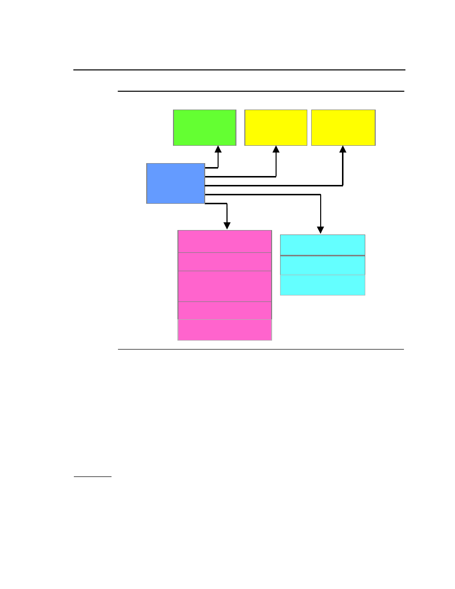
1-10
1
Intel Architecture Optimization Reference Manual
Caches of the Pentium
II
and Pentium III Processors
The on-chip cache subsystem of Pentium II and Pentium
III
processors
consists of two 16-Kbyte four-way set associative caches with a cache line
length of 32 bytes. The caches employ a write-back mechanism and a
pseudo-LRU (least recently used) replacement algorithm. The data cache
consists of eight banks interleaved on four-byte boundaries.
Figure 1-2
Execution Units and Ports in the Out-Of-Order Core
Port 1
Port 3
Port 2
Port 4
Port 0
Reservation
Station
Load
Unit
(16-entry buffer)
Store Address
Calculation
Unit
(12-entry buffer)
Store
Data Unit
(12-entry buffer)
MMX™ technology
Integer
Unit
Pentium(R) III processor
FP Unit
MMX™ technology
Integer
Unit
Address
Generation
Unit
FP Unit
Pentium(R) III processor
FP Unit

Processor Architecture Overview
1
1-11
Level two (L2) caches have been off chip but in the same package. They are
128K or more in size. L2 latencies are in the range of 4 to 10 cycles. An L2
miss initiates a transaction across the bus to memory chips. Such an access
requires on the order of at least 11 additional bus cycles, assuming a DRAM
page hit. A DRAM page miss incurs another three bus cycles. Each bus
cycle equals several processor cycles, for example, one bus cycle for a
100 MHz bus is equal to four processor cycles on a 400 MHz processor. The
speed of the bus and sizes of L2 caches are implementation dependent,
however. Check the specifications of a given system to understand the
precise characteristics of the L2 cache.
Store Buffers
Pentium II and Pentium
III
processors have twelve store buffers. These
processors temporarily store each write (store) to memory in a store buffer.
The store buffer improves processor performance by allowing the processor
to continue executing instructions without having to wait until a write to
memory and/or cache is complete. It also allows writes to be delayed for
more efficient use of memory-access bus cycles.
Writes stored in the store buffer are always written to memory in program
order. Pentium II and Pentium
III
processors use processor ordering to
maintain consistency in the order in which data is read (loaded) and written
(stored) in a program and the order in which the processor actually carries
out the reads and writes. With this type of ordering, reads can be carried out
speculatively; and in any order, reads can pass buffered writes, while writes
to memory are always carried out in program order.
Write hits cannot pass write misses, so performance of critical loops can be
improved by scheduling the writes to memory. When you expect to see
write misses, schedule the write instructions in groups no larger than
twelve, and schedule other instructions before scheduling further write
instructions.

1-12
1
Intel Architecture Optimization Reference Manual
Streaming SIMD Extensions of the Pentium III
Processor
The Streaming SIMD Extensions of the Pentium
III
processor accelerate
performance of applications over the Pentium II processors, for example,
3D graphics. The programming model is similar to the MMX™ technology
model except that instructions now operate on new packed floating-point
data types, which contain four single-precision floating-point numbers.
The Streaming SIMD Extensions of the Pentium
III
processor introduce new
general purpose floating-point instructions, which operate on a new set of
eight 128-bit Streaming SIMD Extensions registers. This gives the
programmer the ability to develop algorithms that can mix packed
single-precision floating-point and integer using both Streaming SIMD
Extensions and MMX instructions respectively. In addition to these
instructions, Streaming SIMD Extensions technology also provide new
instructions to control cacheability of all data types. These include ability to
stream data into the processor while minimizing pollution of the caches and
the ability to prefetch data before it is actually used. Both 64-bit integer and
packed floating point data can be streamed to memory.
The main focus of packed floating-point instruction is the acceleration of
3D geometry. The new definition also contains additional SIMD integer
instructions to accelerate 3D rendering and video encoding and decoding.
Together with the cacheability control instructions, this combination
enables the development of new algorithms that can significantly accelerate
3D graphics and other applications that involve intensive computation.
The new Streaming SIMD Extensions state requires operating system
support for saving and restoring the new state during a context switch. A
new set of extended
fsave/frstor
(called
fxsave/fxrstor
) permits
saving/restoring new and existing state for applications and operating
systems. To make use of these new instructions, an application must verify
that the processor and operating system support Streaming SIMD
Extensions. If both do, then the software application can use the new
features.

Processor Architecture Overview
1
1-13
The Streaming SIMD Extensions are fully compatible with all software
written for Intel architecture microprocessors. All existing software
continues to run correctly, without modification, on microprocessors that
incorporate the Streaming SIMD Extensions, as well as in the presence of
existing and new applications that incorporate this technology.
Single-Instruction, Multiple-Data (SIMD)
The Streaming SIMD Extensions support operations on packed
single-precision floating-point data types, and the additional SIMD integer
instructions support operations on packed quadword data types (byte, word,
or double-word). This approach was chosen because most 3D graphics and
digital signal processing (DSP) applications have the following
characteristics:
•
inherently parallel
•
wide dynamic range, hence floating-point based
•
regular and re-occurring memory access patterns
•
localized re-occurring operations performed on the data
•
data-independent control flow.
Streaming SIMD Extensions fully support the IEEE Standard 754 for
Binary Floating-Point Architecture. The Streaming SIMD Extensions are
accessible from all IA execution modes: protected mode, real-address
mode, and Virtual 8086 mode.
New Data Types
The principal data type of the Streaming SIMD Extensions are a packed
single-precision floating-point operand, specifically four 32-bit
single-precision (SP) floating-point numbers shown in Figure 1-3. The
SIMD integer instructions operate on the packed byte, word, or
double-word data types. The prefetch instructions work on a cache line
granularity regardless of type.

1-14
1
Intel Architecture Optimization Reference Manual
Streaming SIMD Extensions Registers
The Streaming SIMD Extensions provide eight 128-bit general-purpose
registers, each of which can be directly addressed. These registers are a new
state, requiring support from the operating system to use them. They can
hold packed, 128-bit data, and are accessed directly by the Streaming SIMD
Extensions using the register names XMM0 to XMM7, see Figure 1-4.
Figure 1-3
Streaming SIMD Extensions Data Type
Figure 1-4
Streaming SIMD Extensions Register Set
127
96 95
64 63
32 31
0
Packed, single-precision FP
127
0
XMM7
XMM6
XMM5
XMM4
XMM3
XMM2
XMM1
XMM0

Processor Architecture Overview
1
1-15
MMX™ Technology
Intel’s MMX™
technology is an extension to the Intel architecture (IA)
instruction set. The technology uses a single instruction, multiple data
(SIMD) technique to speed up multimedia and communications software by
processing data elements in parallel. The MMX instruction set adds 57
opcodes and a 64-bit quadword data type. The 64-bit data type, illustrated in
Figure 1-5, holds packed integer values upon which MMX instructions
operate.
In addition, there are eight 64-bit MMX technology registers, each of which
can be directly addressed using the register names MM0 to MM7.
Figure 1-6 shows the layout of the eight MMX technology registers.
Figure 1-5
MMX Technology 64-bit Data Type
0
7
8
63
Packed Byte: 8 bytes packed into 64-bits
31
32
0
63
Packed Word: Four words packed into 64-bits
0
63
Packed Double-word: Two doublewords packed into 64-bits
15
16
31
32
15
16
31
32

1-16
1
Intel Architecture Optimization Reference Manual
The MMX technology is operating-system-transparent and 100%
compatible with all existing Intel architecture software. Therefore all
applications will continue to run on processors with MMX technology.
Additional information and details about the MMX instructions, data types,
and registers can be found in the Intel Architecture MMX™ Technology
Programmer’s Reference Manual, order number 243007.
Figure 1-6
MMX Technology Register Set
0
63
MM7
10
Tag
Field
MM0

2-1
General Optimization
Guidelines
2
This chapter discusses general optimization techniques that can improve the
performance of applications for the Pentium
®
II and Pentium
III
processor
architectures. It discusses general guidelines as well as specifics of each
guideline and provides examples of how to improve your code.
Integer Coding Guidelines
The following guidelines will help you optimize your code:
•
Use a current generation of compiler, such as the Intel
®
C/C++
Compiler that will produce an optimized application.
•
Write code so that Intel compiler can optimize it for you:
— Minimize use of global variables, pointers, and complex control
flow
— Use the
const
modifier, avoid
register
modifier
— Avoid indirect calls and use the type system
— Use minimum sizes for integer and floating-point data types to
enable SIMD parallelism
•
Improve branch predictability by using the branch prediction
algorithm. This is one of the most important optimizations for Pentium
II processors. Improving branch predictability allows the code to spend
fewer cycles fetching instructions due to fewer mispredicted branches.
•
Take advantage of the SIMD capabilities of MMX™ technology and
Streaming SIMD Extensions.
•
Avoid partial register stalls.
•
Ensure proper data alignment.

2-2
2
Intel Architecture Optimization Reference Manual
•
Arrange code to minimize instruction cache misses and optimize
prefetch.
•
Avoid prefixed opcodes other than 0F.
•
Avoid small loads after large stores to the same area of memory. Avoid
large loads after small stores to the same area of memory. Load and
store data to the same area of memory using the same data sizes and
address alignments.
•
Use software pipelining.
•
Avoid self-modifying code.
•
Avoid placing data in the code segment.
•
Calculate store addresses as early as possible.
•
Avoid instructions that contain four or more µops or instructions that
are more than seven bytes long. If possible, use instructions that require
one µop.
•
Cleanse partial registers before calling callee-save procedures.
Branch Prediction
Branch optimizations are one of the most important optimizations for
Pentium II processors. Understanding the flow of branches and improving
the predictability of branches can increase the speed of your code
significantly.
Dynamic Branch Prediction
Dynamic prediction is always attempted first by checking the branch target
buffer (BTB) for a valid entry. If one is not there, static prediction is used.
Three elements of dynamic branch prediction are important:
•
If the instruction address is not in the BTB, execution is predicted to
continue without branching. This is known as “fall-through” meaning
that the branch is not taken and the subsequent instruction is executed.
•
Predicted taken branches have a one clock delay.
•
The Pentium II and Pentium
III
processors’ BTB pattern matches on the
direction of the last four branches to dynamically predict whether a
branch will be taken.

General Optimization Guidelines
2
2-3
During the process of instruction prefetch the address of a conditional
instruction is checked with the entries in the BTB. When the address is not
in the BTB, execution is predicted to fall through to the next instruction.
This suggests that branches should be followed by code that will be
executed. The code following the branch will be fetched, and in the case of
Pentium Pro, Pentium II processors, and Pentium
III
processor the fetched
instructions will be speculatively executed. Therefore, never follow a
branch instruction with data.
Additionally, when an instruction address for a branch instruction is in the
BTB and it is predicted taken, it suffers a one-clock delay on Pentium II
processors. To avoid the delay of one clock for taken branches, simply insert
additional work between branches that are expected to be taken. This delay
restricts the minimum duration of loops to two clock cycles. If you have a
very small loop that takes less than two clock cycles, unroll it to remove the
one-clock overhead of the branch instruction.
The branch predictor on Pentium II processors correctly predicts regular
patterns of branches—up to a length of four. For example, it correctly
predicts a branch within a loop that is taken on odd iterations, and not taken
on even iterations.
Static Prediction
On Pentium II and Pentium
III
processors, branches that do not have a
history in the BTB are predicted using a static prediction algorithm as
follows:
•
Predict unconditional branches to be taken.
•
Predict backward conditional branches to be taken. This rule is suitable
for loops.
•
Predict forward conditional branches to be NOT taken.
A branch that is statically predicted can lose, at most, six cycles of
instruction prefetch. An incorrect prediction suffers a penalty of greater than
twelve clocks. Example 2-1 provides the static branch prediction algorithm.

2-4
2
Intel Architecture Optimization Reference Manual
Example 2-1 and Example 2-2 illustrate the basic rules for the static
prediction algorithm.
In the above example, the backward branch
(JC Begin
) is not in the BTB
the first time through, therefore, the BTB does not issue a prediction. The
static predictor, however, will predict the branch to be taken, so a
misprediction will not occur.
Figure 2-1
Pentium
®
II
Processor Static Branch Prediction Algorithm
Example 2-1 Prediction Algorithm
Begin: mov eax, mem32
and eax, ebx
imul eax, edx
shld eax, 7
JC Begin
cond i t i onal br anches n ot tak en (fal l t hr ou gh)
I f < cond i t i on> {
...
}
U n cond i t i onal Br anch es t ak en
f or <cond i t i on> {
...
}
Back w ar d Cond i t i onal Br anches ar e t ak en
l oop {
} <cond i t i on >
Forward
JMP

General Optimization Guidelines
2
2-5
The first branch instruction (
JC Begin
) in Example 2-3 segment is a
conditional forward branch. It is not in the BTB the first time through, but
the static predictor will predict the branch to fall through
.
The
Call Convert
instruction will not be predicted in the BTB the first
time it is seen by the BTB, but the call will be predicted as taken by the
static prediction algorithm. This is correct for an unconditional branch.
In these examples, the conditional branch has only two alternatives: taken
and not taken. Indirect branches, such as switch statements, computed
GOTO
s or calls through pointers, can jump to an arbitrary number of
locations. Assuming the branch has a skewed target destination, and most of
the time it branches to the same address, then the BTB will predict
accurately most of the time. If, however, the target destination is not
predictable, performance can degrade quickly. Performance can be
improved by changing the indirect branches to conditional branches that can
be predicted.
Eliminating and Reducing the Number of Branches
Eliminating branches improves performance due to:
•
Reducing the possibility of mispredictions.
•
Reducing the number of required BTB entries.
Using the
setcc
instruction, or using the Pentium II and Pentium
III
processors’ conditional move (
cmov
or
fcmov
) instructions can eliminate
branches.
Example 2-2 Misprediction Example
mov eax, mem32
and eax, ebx
imul eax, edx
shld eax, 7
JC Begin
mov eax, 0
Begin Call Convert

2-6
2
Intel Architecture Optimization Reference Manual
Following is a C code line with a condition that is dependent upon one of
the constants:
X = (A < B) ? C1 : C2;
This code conditionally compares two values,
A
and
B
. If the condition is
true,
X
is set to
C1
; otherwise it is set to
C2
. The assembly equivalent is
shown in the Example 2-3:
If you replace the
jge
instruction in the previous example with a
setcc
instruction, this code can be optimized to eliminate the branches as shown
in the Example 2-4:
The optimized code sets
ebx
to zero, then compares
A
and
B
. If
A
is greater
than or equal to
B
,
ebx
is set to one. Then
ebx
is decreased and “
and
-ed”
with the difference of the constant values. This sets
ebx
to either zero or the
Example 2-3 Assembly Equivalent of Conditional C Statement
cmp A, B
; condition
jge L30
; conditional branch
mov ebx, CONST1 ; ebx holds X
jmp L31
; unconditional branch
L30:
mov ebx, CONST2
L31:
Example 2-4 Code Optimization to Eliminate Branches
xor ebx, ebx
;clear ebx (X in the C code)
cmp A, B
setge ebx
;When ebx = 0 or 1
;OR the complement condition
dec ebx
;ebx=00...00 or 11...11
and ebx, (CONST1-CONST2);ebx=0 or(CONST1-CONST2)
add ebx, CONST2
;ebx=CONST1 or CONST2

General Optimization Guidelines
2
2-7
difference of the values. By adding
CONST2
back to
ebx
, the correct value is
written to
ebx
. When
CONST1
is equal to zero, the last instruction can be
deleted.
Another way to remove branches on Pentium II and Pentium
III
processors
is to use the
cmov
and
fcmov
instructions. Example 2-5 shows changing a
test and branch instruction sequence using
cmov
and eliminating a branch.
If the test sets the equal flag, the value in
ebx
will be moved to
eax
. This
branch is data-dependent, and is representative of an unpredictable branch.
The label
1h:
is no longer needed unless it is the target of another branch
instruction.
The
cmov
and
fcmov
instructions are available on the Pentium Pro,
Pentium II and Pentium
III
processors, but not on Pentium processors and
earlier 32-bit Intel architecture-based processors. Be sure to check whether
a processor supports these instructions with the
cpuid
instruction if an
application needs to run on older processors as well.
Example 2-5 Eliminating Branch with CMOV Instruction
test ecx, ecx
jne 1h
mov eax, ebx
1h:
; To change the code, the jne and the mov instructions
; are combined into one cmovcc instruction that checks
; the equal flag. The optimized code is:
test ecx, ecx ; test the flags
cmoveq eax, ebx ; if the equal flag is set, move
; ebx to eax
1h:

2-8
2
Intel Architecture Optimization Reference Manual
Performance Tuning Tip for Branch Prediction
Intel C/C++ Compiler has a
-Qxi
switch which turns on Pentium II or
Pentium
III
processor-specific code generation so that the compiler will
generate
cmov-/fcmov
instruction sequences when possible, saving you
the effort of doing it by hand.
For information on branch elimination, see the Pentium II Processor
Computer Based Training (CBT), which is available with the VTune™
Performance Enhancement Environment CD at
http://developer.intel.com/vtune
In addition to eliminating branches, the following guidelines improve
branch predictability:
•
Ensure that each call has a matching return.
•
Don’t intermingle data and instructions.
•
Unroll very short loops.
•
Follow static prediction algorithm.
When a misprediction occurs the entire pipeline is flushed up to the branch
instruction and the processor waits for the mispredicted branch to retire.
Branch Misprediction Ratio =
BR_Miss_Pred_Ret
/
BR_Inst_Ret
If the branch misprediction ratio is less than about 5% then branch
prediction is within normal range. Otherwise, identify the branches that
cause significant mispredictions and try to remedy the situation using the
techniques described in the “Eliminating and Reducing the Number of
Branches” earlier in this chapter.
Partial Register Stalls
On Pentium II and Pentium
III
processors, when a 32-bit register (for
example,
eax
) is read immediately after a 16- or 8-bit register (for example,
al
,
ah
,
ax
) is written, the read is stalled until the write retires, after a
minimum of seven clock cycles. Consider Example 2-6. The first instruction
moves the value 8 into the
ax
register. The following instruction accesses
the register
eax
. This code sequence results in a partial register stall as
shown in Example 2-6.

General Optimization Guidelines
2
2-9
This applies to all of the 8- and 16-bit/32-bit register pairs, listed below:
Small Registers
Large Registers:
al
ah
ax
eax
bl
bh
bx
ebx
cl
ch
cx
ecx
dl
dh
dx
edx
sp
esp
bp
ebp
di
edi
si
esi
Pentium processors do not exhibit this penalty.
Because Pentium II and Pentium
III
processors can execute code out of
order, the instructions need not be immediately adjacent for the stall to
occur. Example 2-7 also contains a partial stall.
In addition, any µops that follow the stalled µop also wait until the clock
cycle after the stalled µop continues through the pipe. In general, to avoid
stalls, do not read a large (32-bit) register (
eax
) after writing a small (8- or
16-bit) register (
al
or
ax
) which is contained in the large register.
Special cases of reading and writing small and large register pairs are
implemented in Pentium II and Pentium
III
processors in order to simplify
the blending of code across processor generations. The special cases are
implemented for
xor
and
sub
when using
eax
,
ebx
,
ecx
,
edx
,
ebp
,
esp
,
Example 2-6 Partial Register Stall
MOV ax, 8
ADD ecx, eax
; Partial stall occurs on access
; of the EAX register
Example 2-7 Partial Register Stall with Pentium
II
and Pentium III Processors
MOV al, 8
MOV edx, 0x40
MOV edi, new_value
ADD edx, eax ; Partial stall accessing EAX

2-10
2
Intel Architecture Optimization Reference Manual
edi
, and
esi
as shown in the A. through E. series in. Generally, when
implementing this sequence, always zero the large register and then write to
the lower half of the register.
Performance Tuning Tip for Partial Stalls
Partial stalls can be measured by selecting the Partial Stall Events or Partial
Stall Cycles events in the VTune Performance Analyzer and running a
sampling on your application. Partial Stall Events show the number of
events and Partial Stall Cycles show the number of cycles for partial stalls,
respectively. To select the events, in the VTune analyzer, click on Configure
menu\Options command\Processor Events for EBS for the list of all
processor events, select one of the above events and double click on it. The
Example 2-8 Simplifying the Blending of Code in Pentium
II
and Pentium III
Processors
A.
xor eax, eax
movb al, mem8
add eax, mem32
; no partial stall
B.
xor eax, eax
movw ax, mem16
add eax, mem32
; no partial stall
C.
sub ax, ax
movb al, mem8
add ax, mem16
; no partial stall
D.
sub eax, eax
movb al, mem8
or ax, mem16
; no partial stall
E.
xor ah, ah
movb al, mem8
sub ax, mem16
; no partial stall

General Optimization Guidelines
2
2-11
Events Customization window opens where you can set the Counter Mask
for either of those events. For more details, see
for Optimization” in Chapter 7
. If a particular stall occurs more than about
3% of the execution time, then the code associated with this stall should be
modified to eliminate the stall. Intel C/C++ Compiler at the default
optimization level (switch
-O2
) ensures that partial stalls do not occur in the
generated code.
Alignment Rules and Guidelines
This section discusses guidelines for alignment of both code and data. On
Pentium II and Pentium
III
processors, a misaligned access that crosses a
cache line boundary does incur a penalty. A Data Cache Unit (DCU) split is
a memory access that crosses a 32-byte line boundary. Unaligned accesses
may cause a DCU split and stall Pentium II and Pentium
III
processors. For
best performance, make sure that in data structures and arrays greater than
32 bytes, the structure or array elements are 32-byte-aligned and that access
patterns to data structure and array elements do not break the alignment
rules.
Code
Pentium II and Pentium
III
processors have a cache line size of 32 bytes.
Since the instruction prefetch buffers fetch on 16-byte boundaries, code
alignment has a direct impact on prefetch buffer efficiency.
For optimal performance across the Intel architecture family, the following
is recommended:
•
Loop entry labels should be 16-byte-aligned when less than eight bytes
away from a 16-byte boundary.
•
Labels that follow a conditional branch need not be aligned.
•
Labels that follow an unconditional branch or function call should be
16-byte-aligned when less than eight bytes away from a 16-byte
boundary.
•
Use a compiler that will assure these rules are met for the generated
code.

2-12
2
Intel Architecture Optimization Reference Manual
On Pentium II and Pentium
III
processors, avoid loops that execute in less
than two cycles. The target of the tight loops should be aligned on a 16-byte
boundary to maximize the use of instructions that will be fetched. On
Pentium II and Pentium
III
processors, it can limit the number of
instructions available for execution, limiting the number of instructions
retired every cycle. It is recommended that critical loop entries be located
on a cache line boundary. Additionally, loops that execute in less than two
cycles should be unrolled. See section
“MMX™ Technology” in Chapter 1
for more information about decoding on the Pentium II and Pentium
III
processors.
Data
A misaligned data access that causes an access request for data already in
the L1 cache can cost six to nine cycles. A misaligned access that causes an
access request from L2 cache or from memory, however, incurs a penalty
that is processor-dependent. Align the data as follows:
•
Align 8-bit data at any address.
•
Align 16-bit data to be contained within an aligned four byte word.
•
Align 32-bit data so that its base address is a multiple of four.
•
Align 64-bit data so that its base address is a multiple of eight.
•
Align 80-bit data so that its base address is a multiple of sixteen.
A 32-byte or greater data structure or array should be aligned so that the
beginning of each structure or array element is aligned in a way that its base
address is a multiple of thirty-two.
Data Cache Unit (DCU) Split
Figure 2-1 shows the type of code that can cause a cache split. The code
loads the addresses of two
dword
arrays. In this example, every four
iterations of the first two dword loads cause a cache split. The data declared
at address 029e70feh is not 32-byte-aligned, therefore each load to this
address and every load that occurs 32 bytes (every four iterations) from this
address will cross the cache line boundary. When the misaligned data
crosses a cache line boundary it causes a six- to twelve-cycle stall.
.
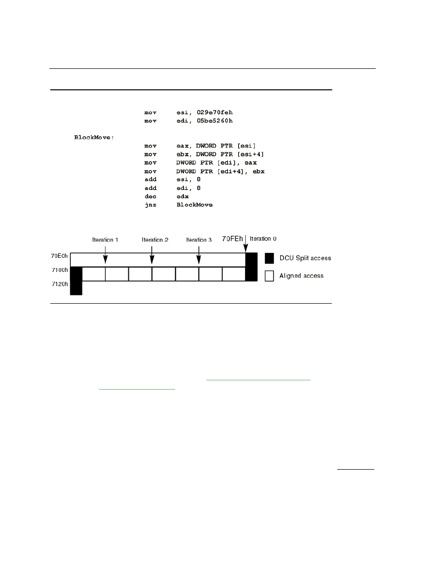
General Optimization Guidelines
2
2-13
Performance Tuning Tip for Misaligned Accesses
Misaligned data can be detected by using the Misaligned Accesses event
counter on Pentium II and Pentium
III
processors. Use the VTune analyzer’s
dynamic execution functionality to determine the exact location of a
misaligned access. Code and data rearrangements for optimal memory
usage are discussed in Chapter 6, “
Optimizing Cache Utilization for
Figure 2-2
DCU Split in the Data Cache

2-14
2
Intel Architecture Optimization Reference Manual
Instruction Scheduling
Scheduling or pipelining should be done in a way that optimizes
performance across all processor generations. The following section
presents scheduling rules that can improve the performance of your code on
Pentium II and Pentium
III
processors.
Scheduling Rules for Pentium II and Pentium III Processors
Pentium II and Pentium
III
processors have three decoders that translate
Intel architecture (IA) macroinstructions into µops as discussed in
Chapter 1, “
Processor Architecture Overview
.” The decoder limitations are
as follows:
•
In each clock cycle, the first decoder is capable of decoding one
macroinstruction made up of four or fewer µops. It can handle any
number of bytes up to the maximum of 15, but nine-or-more-byte
instructions require additional cycles.
•
In each clock cycle, the other two decoders can each decode an
instruction of one µop, and up to eight bytes. Instructions composed of
more than four µops take multiple cycles to decode.
Appendix C, “
Instruction to Decoder Specification
,” contains a table of all
Intel macroinstructions with the number of µops into which they are
decoded. Use this information to determine the decoder on which they can
be decoded.
The macroinstructions entering the decoder travel through the pipe in order,
therefore if a macroinstruction will not fit in the next available decoder, the
instruction must wait until the next cycle to be decoded. It is possible to
schedule instructions for the decoder so that the instructions in the in-order
pipeline are less likely to be stalled.
Consider the following code series in Example 2-9.

General Optimization Guidelines
2
2-15
The sections of Example 2-9 are explained as follows:
A. If the next available decoder for a multi-µop instruction is not decoder 0,
the multi-op instruction will wait for decoder 0 to be available; this usu-
ally happens in the next clock, leaving the other decoders empty during
the current clock. Hence, the following two instructions will take two
cycles to decode.
B. During the beginning of the decoding cycle, if two consecutive instruc-
tions are more than one µop, decoder 0 will decode one instruction and
the next instruction will not be decoded until the next cycle.
C. Instructions of the
op reg, mem
type require two µops: the load from
memory and the operation µop. Scheduling for the decoder template
(4-1-1) can improve the decoding throughput of your application.
In general,
op reg, mem
forms of instructions are used to reduce
register pressure in code that is not memory bound, and when the data
is in the cache. Use simple instructions for improved speed on Pentium
II and Pentium
III
processors.
Example 2-9 Scheduling Instructions for the Decoder
A.
add eax, ecx
; 1 µop instruction (decoder 0)
add edx, [ebx]
; 2 µop instruction (stall 1 cycle
; wait till decoder 0 is available)
B.
add eax, [ebx]
; 2 µop instruction (decoder 0)
mov [eax], ecx
; 2 µop instruction (stall 1 cycle
; to wait until decoder 0 is available)
C.
add eax, [ebx]
; 2 µop instruction (decoder 0)
mov ecx, [eax]
; 2 µop instruction (stall 1 cycle
; to wait until decoder 0 is available)
add ebx, 8
; 1 µop instruction (decoder 1)
D.
pmaddwd mm6, [ebx]; 2 µops instruction (decoder 0)
paddd mm7, mm6
; 1 µop instruction (decoder 1)
add ebx, 8
; 1 µop instruction (decoder 2)

2-16
2
Intel Architecture Optimization Reference Manual
D. The following rules should be observed while using the
op reg, mem
instruction with MMX technology: when scheduling, keep in mind the
decoder template (4-1-1) on Pentium II and Pentium
III
processors, as
shown in Example 2-10, D.
Prefixed Opcodes
On the Pentium II and Pentium
III
processors, avoid the following prefixes:
•
lock
•
segment override
•
address size
•
operand size
On Pentium II and Pentium
III
processors, instructions longer than seven
bytes limit the number of instructions decoded in each cycle. Prefixes add
one to two bytes to the length of instruction, possibly limiting the decoder.
Whenever possible, avoid prefixing instructions. Schedule them behind
instructions that themselves stall the pipe for some other reason.
Pentium II and Pentium
III
processors can only decode one instruction at a
time when an instruction is longer than seven bytes. So for best
performance, use simple instructions that are less than eight bytes in length.
Performance Tuning Tip for Instruction Scheduling
Intel C/C++ Compiler generates highly optimized code specifically for the
Intel architecture-based processors. For assembly code applications, you
can use the assembly coach of the VTune analyzer to get a scheduling
advice, see Chapter 7, “
Instruction Selection
The following sections explain which instruction sequences to avoid or use
when generating optimal assembly code.

General Optimization Guidelines
2
2-17
The Use of
lea
Instruction
In many cases a
lea
instruction or a sequence of
lea
,
add
,
sub
,
and
shift
instructions can be used to replace constant multiply instructions.
Use the integer multiply instruction to optimize code designed for
Pentium II and Pentium
III
processors. The
lea
instruction can be used
sometimes as a three/four operand addition instruction, for example,
lea ecx, [eax+ebx+4+a]
Using the
lea
instruction in this way can avoid some unnecessary register
usage by not tying up registers for the operands of some arithmetic
instructions.
On the Pentium II and Pentium
III
processors, both
lea
and
shift
instructions are single µop instructions that execute in one cycle. However,
that short latency may not persist in future implementations. The Intel
C/C++ Compiler checks to ensure that these instructions are used correctly
whenever possible.
For the best blended code, replace the
shift
instruction with two or more
add
instructions, since the short latency of this instruction may not be
maintained across all implementations.
Complex Instructions
Avoid using complex instructions (for example,
enter
,
leave
, or
loop
)
that generally have more than four µops and require multiple cycles to
decode. Use sequences of simple instructions instead.
Short Opcodes
Use one-byte instructions as much as possible. This reduces code size and
increases instruction density in the instruction cache. For example, use the
push
and
pop
instructions instead of
mov
instructions to save registers to
the stack.

2-18
2
Intel Architecture Optimization Reference Manual
8/16-bit Operands
With eight-bit operands, try to use the byte opcodes, rather than using 32-bit
operations on sign and zero-extended bytes. Prefixes for operand size
override apply to 16-bit operands, not to eight-bit operands.
Sign extension is usually quite expensive. Often, the semantics can be
maintained by zero-extending 16-bit operands. For example, the C code in
the following statements does not need sign extension, nor does it need
prefixes for operand size overrides:
static short int a, b;
if (a==b) {
. . .
}
Code for comparing these 16-bit operands might be:
xor eax, eax
xor ebx, ebx
movw ax, [a]
movw bx, [b]
cmp eax, ebx
Of course, this can only be done under certain circumstances, but the
circumstances tend to be quite common. This would not work if the
compare was for greater than, less than, greater than or equal, and so on, or
if the values in
eax
or
ebx
were to be used in another operation where sign
extension was required.
movsw eax, a ; 1 prefix + 3
movsw ebx, b ; 5
cmp ebx, eax ; 9
Pentium II and Pentium
III
processors provide special support to
XOR
a
register with itself, recognizing that clearing a register does not depend on
the old value of the register. Additionally, special support is provided for the
above specific code sequence to avoid the partial stall. See
section for more information.
The performance of the
movzx
instructions has been improved in order to
reduce the prevalence of partial stalls on Pentium II and Pentium
III
processors. Use the
movzx
instructions when coding for these processors.

General Optimization Guidelines
2
2-19
Comparing Register Values
Use
test
when comparing a value in a register with zero.
Test
essentially
and
s the operands together without writing to a destination register.
Test
is
preferred over
and
because
and
writes the result register, which may
subsequently cause an artificial output dependence on the processor.
Test
is better than
cmp .., 0
because the instruction size is smaller.
Use
test
when comparing the result of a logical
and
with an immediate
constant for equality or inequality if the register is
eax
for cases such as:
if (avar & 8) { }
Address Calculations
Pull address calculations into load and store instructions. Internally,
memory reference instructions can have four operands:
•
relocatable load-time constant
•
immediate constant
•
base register
•
scaled index register.
In the segmented model, a segment register may constitute an additional
operand in the linear address calculation. In many cases, several integer
instructions can be eliminated by fully using the operands of memory
references.
Clearing a Register
The preferred sequence to move zero to a register is:
xor
reg
, reg
This saves code space but sets the condition codes. In contexts where the
condition codes must be preserved, move
0
into the register:
mov reg, 0

2-20
2
Intel Architecture Optimization Reference Manual
Integer Divide
Typically, an integer divide is preceded by a
cdq
instruction. Divide
instructions use
EDX:EAX
as the dividend and
cdq
sets up
EDX
. It is better to
copy
EAX
into
EDX
, then right-shift
EDX
31 places to sign-extend. If you
know that the value is positive, use sequence
xor
edx
,
edx
On Pentium II and Pentium
III
processors, the
cdq
instruction is faster since
cdq
is a single µop instruction as opposed to two instructions for the
copy/shift
sequence.
Comparing with Immediate Zero
Often when a value is compared with zero, the operation produces the value
sets condition codes, which can be tested directly by a
jcc
instruction. The
most notable exceptions are
mov
and
lea
. In these cases, use
test
.
Prolog Sequences
In routines that do not call other routines (leaf routines), use
ESP
as the base
register to free up
EBP
. If you are not using the 32-bit flat model, remember
that
EBP
cannot be used as a general purpose base register because it
references the stack segment.
Epilog Sequences
If only four bytes were allocated in the stack frame for the current function,
use
pop
instructions instead of incrementing the stack pointer by four.
Improving the Performance of Floating-point
Applications
When programming floating-point applications, it is best to start at the C,
C++, or FORTRAN language level. Many compilers perform floating-point
scheduling and optimization when it is possible. However in order to
produce optimal code, the compiler may need some assistance.

General Optimization Guidelines
2
2-21
Guidelines for Optimizing Floating-point Code
Follow these rules to improve the speed of your floating-point applications:
•
Understand how the compiler handles floating-point code.
•
Look at the assembly dump and see what transforms are already
performed on the program.
•
Study the loop nests in the application that dominate the execution
time.
•
Determine why the compiler is not creating the fastest code.
•
See if there is a dependence that can be resolved.
•
Consider large memory bandwidth requirements.
•
Think of poor cache locality improvement.
•
See if there is a lot of long-latency floating-point arithmetic operations.
•
Do not use high precision unless necessary. Single precision (32-bits) is
faster on some operations and consumes only half the memory space as
double precision (64-bits) or double extended (80-bits).
•
Make sure you have fast float-to-int routines. Many libraries do more
work than is necessary; make sure your float-to-int is a fast routine.
•
Make sure your application stays in range. Out of range numbers cause
very high overhead.
•
FXCH
can be helpful by increasing the effective name space. This in
turn allows instructions to be reordered to make instructions available
to be executed in parallel. Out of order execution precludes the need for
using
FXCH
to move instructions for very short distances.
•
Unroll loops and pipeline your code.
•
Perform transformations to improve memory access patterns. Use loop
fusion or compression to keep as much of the computation in the cache
as possible.
•
Break dependency chains.
Improving Parallelism
The Pentium II and Pentium
III
processors have a pipelined floating-point
unit. To achieve maximum throughput from the Pentium II and Pentium
III
processors floating-point unit, schedule properly the floating-point
instructions to improve pipelining. Consider the example in Figure 2-2.

2-22
2
Intel Architecture Optimization Reference Manual
To exploit the parallel capability of the Pentium II and Pentium
III
processors, determine which instructions can be executed in parallel. The
two high-level code statements in the example are independent, therefore
their assembly instructions can be scheduled to execute in parallel, thereby
improving the execution speed, see source code in Example 2-10.
Most floating-point operations require that one operand and the result use
the top of stack. This makes each instruction dependent on the previous
instruction and inhibits overlapping the instructions.
One obvious way to get around this is to imagine that we have a flat
floating-point register file available, rather than a stack. The code is shown
in Example 2-11.
Example 2-10 Scheduling Floating-Point Instructions
A = B + C + D;
E = F + G + H;
fld B
fld F
fadd C
fadd G
fadd D
fadd H
fstp A
fstp E
Example 2-11 Coding for a Floating-Point Register File
fld B
?F1
fadd F1, C
?F1
fld F
?F2
fadd F2,G
?F2
fadd F1,D
?F1
fadd F2,H
?F2
fstp F1
?A
fstp F2
?E

General Optimization Guidelines
2
2-23
In order to implement these imaginary registers we need to use the
FXCH
instruction to change the value on the top of stack. This provides a way to
avoid the top of stack dependency. The
FXCH
instruction uses no extra
execution cycles on Pentium II and Pentium
III
processors. Example 2-12
shows its use.
The
FXCH
instructions move an operand into position for the next
floating-point instruction.
Rules and Regulations of the fxch Instruction
The
fxch
instruction costs no extra cycles on Pentium II and Pentium
III
processors. The instruction is almost “free” and can be used to access
elements in the deeper levels of the floating-point stack instead of storing
them and then loading them again.
Example 2-12 Using the FXCH Instruction
STO
ST1
fld B
⇒
F1
fld B B
fadd C
⇒
F1
fadd C B+C
fld F
⇒
F2
fld F B+C
fadd G
⇒
F2
fadd G F+G B+C
fxch ST(1)
B+C
F+G
fadd D
⇒
F1
fadd D B+C+D F+G
fxch ST(1)
F+G
B+C+D
fadd H
⇒
F2
fadd H F+G+H B+C+D
fxch ST(1)
B+C+D
F+G+H
fstp D
⇒
A
fstp A F+G+H
fstp E
⇒
E
fstp E

2-24
2
Intel Architecture Optimization Reference Manual
Memory Operands
Floating-point operands that are 64-bit operands need to be
eight-byte-aligned. Performing a floating-point operation on a memory
operand instead of on a stack register on Pentium II or Pentium
III
processor, produces two µops, which can limit decoding. Additionally,
memory operands may cause a data cache miss, causing a penalty.
Memory Access Stall Information
Floating-point registers allow loading of 64-bit values as doubles. Instead of
loading single array values that are 8-, 16-, or 32-bits long, consider loading
the values in a single quadword, then incrementing the structure or array
pointer accordingly.
First, the loading and storing of quadword data is more efficient using the
larger quadword data block sizes. Second, this helps to avoid the mixing of
8-, 16-, or 32-bit load and store operations with a 64-bit load and store
operation to the memory address. This avoids the possibility of a memory
access stall on Pentium II and Pentium
III
processors. Memory access stalls
occur when
•
small loads follow large stores to the same area of memory
•
large loads follow small stores to the same area of memory.
Consider the following cases in Example 2-13. In the first case (A), there is
a large load after a series of small stores to the same area of memory
(beginning at memory address
mem
), and the large load will stall.
The
fld
must wait for the stores to write to memory before it can access all
the data it requires. This stall can also occur with other data types (for
example, when bytes or words are stored and then words or doublewords are
read from the same area of memory).

General Optimization Guidelines
2
2-25
In the second case (B), there is a series of small loads after a large store to
the same area of memory (beginning at memory address
mem
), and the small
loads will stall.
The word loads must wait for the quadword store to write to memory before
they can access the data they require. This stall can also occur with other
data types (for example, when doublewords or words are stored and then
words or bytes are read from the same area of memory). This can be
avoided by moving the store as far from the loads as possible. In general, the
loads and stores should be separated by at least 10 instructions to avoid the
stall condition.
Floating-point to Integer Conversion
Many libraries provide the float to integer library routines that convert
floating-point values to integer. Many of these libraries conform to ANSI C
coding standards which state that the rounding mode should be truncation.
The default of the
fist
instruction is round to nearest, therefore many
compiler writers implement a change in the rounding mode in the processor
in order to conform to the C and FORTRAN standards. This
implementation requires changing the control word on the processor using
Example 2-13 Large and Small Load Stalls
;A. Large load stall
mov
mem, eax
; store dword to address “mem"
mov
mem + 4, ebx; store dword to address “mem + 4"
:
:
fld
mem
; load qword at address “mem", stalls
;B. Small Load stall
fstp mem ;store qword to address “mem"
:
:
mov bx,mem+2 ;load word at address “mem + 2", stalls
mov cx,mem+4 ;load word at address “mem + 4", stalls

2-26
2
Intel Architecture Optimization Reference Manual
the
fldcw
instruction. This instruction is a synchronizing instruction and
will cause a significant slowdown in the performance of your application on
all IA-based processors.
When implementing an application, consider if the rounding mode is
important to the results. If not, use the algorithm in Example to avoid the
synchronization and overhead of the
fldcw
instruction and changing the
rounding mode.
Example 2-14 Algorithm to Avoid Changing the Rounding Mode
_fto132proc
lea
ecx,[esp-8]
sub
esp,16 ; allocate frame
and
ecx,-8 ; align pointer on boundary of 8
fld
st(0) ; duplicate FPU stack top
fistp
qword ptr[ecx]
fild
qword ptr[ecx]
mov
edx,[ecx+4]; high dword of integer
mov
eax,[ecx]
; low dword of integer
test
eax,eax
je
integer_QnaN_or_zero
continued

General Optimization Guidelines
2
2-27
arg is not integer QnaN:
fsubp
st(1),st ; TOS=d-round(d),
; { st(1)=st(1)-st & pop ST)
test
edx,edx ; what’s sign of integer
jns
positive ; number is negative
; dead cycle
; dead cycle
fstp
dword ptr[ecx]; result of subtraction
mov
ecx,[ecx] ; dword of diff(single-
; precision)
add
esp,16
xor
ecx,80000000h
add
ecx,7fffffffh ; if diff<0 then decrement
; integer
adc
eax,0 ; inc eax (add CARRY flag)
ret
positive:
fstp
dword ptr[ecx]; 17-18 result of
subtraction
mov
ecx,[ecx] ; dword of diff(single-
; precision)
add
esp,16
add
ecx,7fffffffh ; if diff<0 then decrement
; integer
sbb
eax,0 ; dec eax (subtract CARRY flag)
ret
integer_QnaN_or_zero:
test
edx,7fffffffh
jnz
arg_is_not_integer_QnaN
add esp,16
ret
Example 2-14 Algorithm to Avoid Changing the Rounding Mode (continued)

2-28
2
Intel Architecture Optimization Reference Manual
Loop Unrolling
The benefits of unrolling loops are:
•
Unrolling amortizes the branch overhead. The BTB is good at
predicting loops on Pentium II and Pentium
III
processors and the
instructions to increment the loop index and jump are inexpensive.
•
Unrolling allows you to aggressively schedule (or pipeline) the loop to
hide latencies. This is useful if you have enough free registers to keep
variables live as you stretch out the dependency chain to expose the
critical path.
•
You can aggressively schedule the loop to better set up I-fetch and
decode constraints.
•
The backwards branch (predicted as taken) has only a 1 clock penalty
on Pentium II and Pentium
III
processors, so you can unroll very tiny
loop bodies for free.
You can use a
-Qunroll
option of the Intel C/C++ Compiler, see Intel
C/C++ Compiler User’s Guide for Win32* Systems, order number 718195.
Unrolling can expose other optimizations, as shown in Example 2-15. This
example illustrates a loop executes 100 times assigning
x
to every
even-numbered element and
y
to every odd-numbered element.
By unrolling the loop you can make both assignments each iteration,
removing one branch in the loop body.
Example 2-15 Loop Unrolling
Before unrolling:
do i=1,100
if (i mod 2 == 0) then a(i) = x
else a(i) = y
enddo
After unrolling
do i=1,100,2
a(i) = y
a(i+1) = x
enddo

General Optimization Guidelines
2
2-29
Floating-Point Stalls
Many of the floating-point instructions have a latency greater than one cycle
but, because of the out-of-order nature of Pentium II and Pentium
III
processors, stalls will not necessarily occur on an instruction or µop basis.
However, if an instruction has a very long latency such as an
fdiv
, then
scheduling can improve the throughput of the overall application. The
following sections discuss scheduling issues and offer good tips for any
IA-based processor.
Hiding the One-Clock Latency of a Floating-Point Store
A floating-point store must wait an extra cycle for its floating-point
operand. After an
fld
, an
fst
must wait one clock. After the common
arithmetic operations,
fmul
and
fadd
, which normally have a latency of
three,
fst
waits an extra cycle for a total of four. This set also includes
other instructions, for example,
faddp
and
fsubrp
Example 2-16 Hiding One-Clock Latency
; Store is dependent on the previous load.
fld
meml
; 1 fld takes 1 clock
; 2 fst waits, schedule something here
fst
mem2
; 3,4 fst takes 2 clocks
fadd
meml
; 1 add takes 3 clocks
; 2 add, schedule something here
; 3 add, schedule something here
; 4 fst waits, schedule something here
fst
mem2
; 5,2 fst takes 2 clocks
; Store is not dependent on the previous load:
fld
meml
; 1
fld
mem2
; 2
fxch
st(l)
; 2
fst
mem3
; 3 stores values loaded from meml
; A register may be used immediately after it has
; been loaded (with FLD):
fld
mem1
; l
fadd
mem2
; 2,3,4

2-30
2
Intel Architecture Optimization Reference Manual
Use of a register by a floating-point operation immediately after it has been
written by another
fadd
,
fsub
, or
fmul
causes a two-cycle delay. If
instructions are inserted between these two, then latency and a potential stall
can be hidden.
Additionally, while the multi-cycle floating-point instructions,
fdiv
and
fsqrt
, execute in the floating-point unit pipe, integer instructions can be
executed in parallel. Emitting a number of integer instructions after such an
instruction as
fdiv
or
fsqrt
will keep the integer execution units busy.
The exact number of instructions depends on the floating-point instruction’s
cycle count.
Integer and Floating-point Multiply
The integer multiply operations,
mul
and
imul
, are executed in the
floating-point unit so these instructions cannot be executed in parallel with a
floating-point instruction.
A floating-point multiply instruction (
fmul
) delays for one cycle if the
immediately preceding cycle executed an
fmul
or an
fmul
/
fxch
pair. The
multiplier can only accept a new pair of operands every other cycle.
For the best blended code, replace the integer multiply instruction with two
or more
add
instructions, since the short latency of this instruction may not
be maintained across all implementations
Floating-point Operations with Integer Operands
Floating-point operations that take integer operands (
fiadd
or
fisub
..)
should be avoided. These instructions should be split into two instructions:
fild
and a floating-point operation. The number of cycles before another
instruction can be issued (throughput) for
fiadd
is four, while for
fild
and
simple floating-point operations it is one, as shown in the comparison
below.
Complex Instructions
Use These for Potential Overlap
fiadd [ebp] ; 4 fild [ebp] ; 1
faddp st(l) ; 2
Using the
fild - faddp
instructions yields two free cycles for executing
other instructions.

General Optimization Guidelines
2
2-31
FSTSW Instructions
The
fstsw
instruction that usually appears after a floating-point
comparison instruction (
fcom
,
fcomp
,
fcompp
) delays for three cycles.
Other instructions may be inserted after the comparison instruction in order
to hide the latency. On Pentium II and Pentium
III
processors the
fcmov
instruction can be used instead.
Transcendental Functions
If an application needs to emulate these math functions in software, it may
be worthwhile to inline some of these math library calls because the
call
and the prologue/epilogue involved with the calls can significantly affect the
latency of the operations. Emulating these operations in software will not be
faster than the hardware unless accuracy is sacrificed.


3-1
Coding
for SIMD Architectures
3
The capabilities of the Pentium
®
II and Pentium
III
processors enable the
development of advanced multimedia applications. The Streaming SIMD
Extensions and MMX™ technology provide coding extensions to make use
of the processors’ multimedia features, specifically, the single-instruction,
multiple-data (SIMD) characteristics of the instruction set architecture
(ISA). To take advantage of the performance opportunities presented by
these new capabilities, take into consideration the following:
•
Ensure that your processor supports MMX technology and Streaming
SIMD Extensions.
•
Employ all of the optimization and scheduling strategies described in
this book.
•
Use stack and data alignment techniques to keep data properly aligned
for efficient memory use.
•
Utilize the cacheability instructions offered by Streaming SIMD
Extensions.
This chapter gives an overview of the capabilities that allow you to better
understand SIMD features and develop applications utilizing SIMD features
of MMX technology and Streaming SIMD Extensions.

3-2
3
Intel Architecture Optimization Reference Manual
Checking for Processor Support of Streaming SIMD
Extensions and MMX™ Technology
This section shows how to check whether a system supports MMX™
technology and Streaming SIMD Extensions.
Checking for MMX Technology Support
Before you start coding with MMX technology check if MMX technology
is available on your system. Use the
cpuid
instruction to check the feature
flags in the
edx
register. If
cpuid
returns bit 23 set to 1 in the feature flags,
the processor supports MMX technology. Use the code segment in
Example 3-1 to load the feature flags in
edx
and test the result for the
existence of MMX technology.
For more information on
cpuid
see, Intel Processor Identification with
CPUID Instruction, order number 241618. Once this check has been made,
MMX technology can be included in your application in two ways:
1.
Check for MMX technology during installation. If MMX technology is
available, the appropriate DLLs can be installed.
2.
Check for MMX technology during program execution and install the
proper DLLs at runtime. This is effective for programs that may be
executed on different machines.
Example 3-1 Identification of MMX Technology with
cpuid
…identify existence of cpuid instruction
…
;
…
; identify Intel processor
…
;
mov eax, 1
; request for feature flags
cpuid
; 0Fh, 0A2h cpuid instruction
test edx, 00800000h; is MMX technology bit (bit
; 23)in feature flags equal to 1
jnz
Found

Coding for SIMD Architectures
3
3-3
Checking for Streaming SIMD Extensions Support
Checking for support of Streaming SIMD Extensions on your processor is
similar to doing the same for MMX technology, but you must also check
whether your operating system (OS) supports Streaming SIMD Extensions.
This is because the OS needs to manage saving and restoring the new state
introduced by Streaming SIMD Extensions for your application to properly
function.
To check whether your system supports Streaming SIMD Extensions,
follow these steps:
1.
Check that your processor has the
cpuid
instruction and is in the Intel
Pentium II and Pentium
III
processors.
2.
Check the feature bits of
cpuid
for Streaming SIMD Extensions
existence.
3.
Check for OS support for Streaming SIMD Extensions.
shows how to find the Streaming SIMD Extensions feature bit
(bit 25) in the
cpuid
feature flags.
To find out whether the operating system supports Streaming SIMD
Extensions, simply execute a Streaming SIMD Extension and trap for the
exception if one occurs. An invalid opcode will be raised by the operating
system and processor if either is not enabled for Streaming SIMD
Extensions. Catching the exception in a simple try/except clause (using
structured exception handling in C++) and checking whether the exception
code is an invalid opcode will give you the answer. See Example 3-3.
Example 3-2 Identification of Streaming SIMD Extensions with
cpuid
…identify existence of cpuid instruction
…
; identify Intel Processor
mov eax, 1
; request for feature flags
cpuid
; 0Fh, 0A2h cpuid instruction
test EDX, 002000000h; bit 25 in feature flags equal to 1
jnz
Found

3-4
3
Intel Architecture Optimization Reference Manual
Considerations for Code Conversion to SIMD
Programming
The VTune™ Performance Enhancement Environment CD provides tools
to aid in the evaluation and tuning. But before you start implementing them,
you need to know the answers to the following questions:
1.
Will the current code benefit by using MMX technology or Streaming
SIMD Extensions?
2.
Is this code integer or floating-point?
3.
What coding techniques should I use?
4.
What guidelines do I need to follow?
5.
How should I arrange and align the datatypes?
Figure 3-1 provides a flowchart for the process of converting code to MMX
technology or the Streaming SIMD Extensions.
Example 3-3 Identification of Streaming SIMD Extensions by the OS
bool OSSupportCheck() {
_try {
__asm xorps xmm0, xmm0 ;Streaming SIMD Extension
}
_except(EXCEPTION_EXECUTE_HANDLER) {
if (_exception_code()==STATUS_ILLEGAL_INSTRUCTION)
return (false); Streaming SIMD Extensions not supported
}
; Streaming SIMD Extensions are supported by OS
return (true);
}
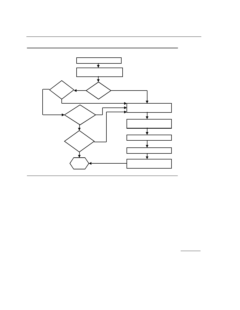
Coding for SIMD Architectures
3
3-5
To use MMX technology or Streaming SIMD Extensions optimally, you
must evaluate the following segments of your code:
•
segments that are computationally intensive
•
segments that require integer implementations that support efficient use
of the cache architecture
•
segments that require floating-point computations.
Figure 3-1
Converting to Streaming SIMD Extensions Chart
1a. Identify hotspots in the code.
1b. Determine if code benefits by
using SIMD technology
.
2a.
FP or Integer?
2b.
Why FP data?
3. Convert the code to use SIMD-
FP or SIMD-Integer
4. Follow the SIMD-Integer or
SIMD-FP coding techniques.
5. Use data alignment rules.
6. Use memory optimizations
7. Use aggressive instruction
scheduling
2c.
Conversion to
Integer without data
loss?
2d.
Convert to
SIMD-FP?
FP data
Range or Precision
No
Performance
Yes
No
Yes
Integer data
Stop

3-6
3
Intel Architecture Optimization Reference Manual
Identifying Hotspots
To optimize performance, you can use the VTune Performance Analyzer to
isolate the computation-intensive sections of code. For details on the VTune
analyzer, see
“VTune™ Performance Analyzer” in Chapter 7
. VTune
analyzer provides a hotspots view of a specific module to help you identify
sections in your code that take the most CPU time and that have potential
performance problems. For more explanation, see section
Analysis for Optimization” in Chapter 7
, which includes an example of a
hotspots report. The hotspots view helps you identify sections in your code
that take the most CPU time and that have potential performance problems.
The VTune analyzer enables you to change the view to show hotspots by
memory location, functions, classes, or source files. You can double-click
on a hotspot and open the source or assembly view for the hotspot and see
more detailed information about the performance of each instruction in the
hotspot.
The VTune analyzer offers focused analysis and performance data at all
levels of your source code and can also provide advice at the assembly
language level. The code coach analyzes and identifies opportunities for
better performance of C/C++, FORTRAN and Java* programs, and
suggests specific optimizations. Where appropriate, the coach displays
pseudo-code to suggest the use of Intel’s highly optimized intrinsics and
functions of the MMX technology and Streaming SIMD Extensions from
Intel
®
Performance Library Suite. Because VTune analyzer is designed
specifically for all of the Intel architecture (IA)-based processors,
Pentium II and Pentium
III
processors in particular, it can offer these
detailed approaches to working with IA. See
, for more details and example of a code coach advice.

Coding for SIMD Architectures
3
3-7
Determine If Code Benefits by Conversion to Streaming SIMD
Extensions
Identifying code that benefits by using MMX technology and/or Streaming
SIMD Extensions can be time-consuming and difficult. Likely candidates
for conversion are applications that are highly computation- intensive such
as the following:
•
speech compression algorithms and filters
•
video display routines
•
rendering routines
•
3D graphics (geometry)
•
image and video processing algorithms
•
spatial (3D) audio
Generally, these characteristics can be identified by the use of small-sized
repetitive loops that operate on integers of 8 or 16 bits for MMX
technology, or single-precision, 32-bit floating-point data for Streaming
SIMD Extensions technology (integer and floating-point data items should
be sequential in memory). The repetitiveness of these loops incurs costly
application processing time. However, these routines have potential for
increased performance when you convert them to use MMX technology or
Streaming SIMD Extensions.
Once you identify your opportunities for using MMX technology or
Streaming SIMD Extensions, you must evaluate what should be done to
determine whether the current algorithm or a modified one will ensure the
best performance.
Coding Techniques
The SIMD features of Streaming SIMD Extensions and MMX technology
require new methods of coding algorithms. One of them is vectorization.
Vectorization is the process of transforming sequentially executing, or
scalar, code into code that can execute in parallel, taking advantage of the
SIMD architecture parallelism. Using this feature is critical for Streaming
SIMD Extensions and MMX technology. This section discusses the coding
techniques available for an application to make use of the SIMD
architecture.

3-8
3
Intel Architecture Optimization Reference Manual
To vectorize your code and thus take advantage of the SIMD architecture,
do the following:
•
Determine if the memory accesses have dependencies that would
prevent parallel execution
•
“Strip-mine” the loop to reduce the iteration count by the length of the
SIMD operations (four for Streaming SIMD Extensions and MMX
technology)
•
Recode the loop with the SIMD instructions
Each of these actions is discussed in detail in the subsequent sections of this
chapter.
Coding Methodologies
Software developers need to compare the performance improvement that
can be obtained from assembly code versus the cost of those improvements.
Programming directly in assembly language for a target platform may
produce the required performance gain, however, assembly code is not
portable between processor architectures and is expensive to write and
maintain.
Performance objectives can be met by taking advantage of the Streaming
SIMD Extensions or MMX technology ISA using high-level languages as
well as assembly. The new C/C++ language extensions designed
specifically for the Streaming SIMD Extensions and MMX technology help
make this possible.
Figure 3-2 illustrates the tradeoffs involved in the performance of hand-
coded assembly versus the ease of programming and portability.
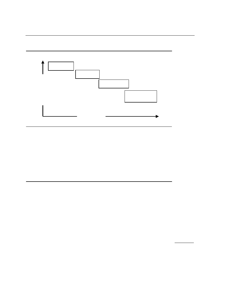
Coding for SIMD Architectures
3
3-9
The examples that follow illustrate the use of assembly coding adjustments
for this new ISA to benefit from the Streaming SIMD Extensions and
C/C++ language extensions. Floating-point data may be used with the
Streaming SIMD Extensions as well as the intrinsics and vector classes with
MMX technology.
As a basis for the usage model discussed in this section, consider a simple
loop shown in Example 3-4.
Example 3-4 Simple Four-Iteration Loop
void add(float *a, float *b, float *c)
{
int i;
for (i = 0; i < 4; i++) {
c[i] = a[i] + b[i];
}
}
_____________________________________________________________
Figure 3-2
Hand-Coded Assembly and High-Level Compiler Performance
Tradeoffs
P
erfo
rm
ance
Portability,
ease of use
Assembly
Intrinsics
C++ classes
Automatic
vectorization

3-10
3
Intel Architecture Optimization Reference Manual
Note that the loop runs for only four iterations. This allows a simple
replacement of the code with Streaming SIMD Extensions.
For the optimal use of the Streaming SIMD Extensions that need data
alignment on the 16-byte boundary, this example assumes that the arrays
passed to the routine,
a
,
b
,
c
, are aligned to 16-byte boundaries by a calling
routine. See Intel application note AP-833, Data Alignment and
Programming Considerations for Streaming SIMD Extensions with the Intel
C/C++ Compiler, order number 243872, for the methods to ensure this
alignment.
The sections that follow detail on the following coding methodologies:
inlined assembly, intrinsics, C++ vector classes, and automatic
vectorization.
Assembly
Key loops can be coded directly in assembly language using an assembler
or by using inlined assembly (C-asm) in C/C++ code. The Intel compiler or
assembler recognizes the new instructions and registers, then directly
generates the corresponding code. This model offers the greatest
performance, but this performance is not portable across the different
processor architectures.
Example 3-5 shows the Streaming SIMD Extensions inlined-asm encoding.
Example 3-5 Streaming SIMD Extensions Using Inlined Assembly Encoding
void add(float *a, float *b, float *c)
{
__asm {
mov eax, a
mov edx, b
mov ecx, c
movaps xmm0, XMMWORD PTR [eax]
addps xmm0, XMMWORD PTR [edx]
movaps XMMWORD PTR [ecx], xmm0
}
}
_____________________________________________________________

Coding for SIMD Architectures
3
3-11
Intrinsics
Intrinsics provide the access to the ISA functionality using C/C++ style
coding instead of assembly language. Intel has defined two sets of intrinsic
functions that are implemented in the Intel C/C++ Compiler to support the
MMX technology and the Streaming SIMD Extensions. Two new C data
types, representing 64-bit and 128-bit objects (
__m64
and
__m128
,
respectively) are used as the operands of these intrinsic functions. This
enables to choose the implementation of an algorithm directly, while also
performing optimal register allocation and instruction scheduling where
possible. These intrinsics are portable among all Intel architecture-based
processors supported by a compiler. The use of intrinsics allows you to
obtain performance close to the levels achievable with assembly. The cost of
writing and maintaining programs with intrinsics is considerably less. For a
detailed description of the intrinsics and their use, refer to the Intel C/C++
Compiler User’s Guide.
Example 3-6 shows the loop from Example 3-4 using intrinsics.
Example 3-6 Simple Four-Iteration Loop Coded with Intrinsics
#include <xmmintrin.h>
void add(float *a, float *b, float *c)
{
__m128 t0, t1;
t0 = _mm_load_ps(a);
t1 = _mm_load_ps(b);
t0 = _mm_add_ps(t0, t1);
_mm_store_ps(c, t0);
}
_____________________________________________________________
The intrinsics map one-to-one with actual Streaming SIMD Extensions
assembly code. The
xmmintrin.h
header file in which the prototypes for
the intrinsics are defined is part of the Intel C/C++ Compiler for Win32*
Systems included with the VTune Performance Enhancement Environment
CD.

3-12
3
Intel Architecture Optimization Reference Manual
Intrinsics are also defined for the MMX technology ISA. These are based on
the
__m64
data type to represent the contents of an
mm
register. You can
specify values in bytes, short integers, 32-bit values, or as a 64-bit object.
The
__m64
and
__m128
data types, however, are not a basic ANSI C data
type, and therefore you must observe the following usage restrictions:
•
Use
__m64
and
__m128
data only on the left-hand side of an
assignment as a return value or as a parameter. You cannot use it with
other arithmetic expressions (“
+
”, “
>>
”, and so on).
•
Use
__m64
and
__m128
objects in aggregates, such as unions to
access the byte elements and structures; the address of an
__m64
object
may be also used.
•
Use
__m64
and
__m128
data only with the MMX intrinsics described
in this guide
.
For complete details of the hardware instructions, see the Intel Architecture
MMX™ Technology Programmer’s Reference Manual. For descriptions of
data types, see the Intel Architecture Software Developer's Manual, Volume
2: Instruction Set Reference Manual.
Classes
Intel has also defined a set of C++ classes to provide both a higher-level
abstraction and more flexibility for programming with MMX technology
and the Streaming SIMD Extensions. These classes provide an easy-to-use
and flexible interface to the intrinsic functions, allowing developers to write
more natural C++ code without worrying about which intrinsic or assembly
language instruction to use for a given operation. Since the intrinsic
functions underlie the implementation of these C++ classes, the
performance of applications using this methodology can approach that of
one using the intrinsics. Further details on the use of these classes can be
found in the Intel C++ Class Libraries for SIMD Operations User’s Guide,
order number 693500.
Example 3-7 shows the C++ code using a vector class library. The example
assumes the arrays passed to the routine are already aligned to 16-byte
boundaries.

Coding for SIMD Architectures
3
3-13
Example 3-7 C++ Code Using the Vector Classes
#include <fvec.h>
void add(float *a, float *b, float *c)
{
F32vec4 *av=(F32vec4 *) a;
F32vec4 *bv=(F32vec4 *) b;
F32vec4 *cv=(F32vec4 *) c;
*cv=*av + *bv
}
_____________________________________________________________
Here,
fvec.h
is the class definition file and
F32vec4
is the class
representing an array of four floats. The “+” and “=” operators are
overloaded so that the actual Streaming SIMD Extensions implementation
in the previous example is abstracted out, or hidden, from the developer.
Note how much more this resembles the original code, allowing for simpler
and faster programming.
Again, the example is assuming the arrays passed to the routine are already
aligned to 16-byte boundary.
Automatic Vectorization
The Intel C/C++ Compiler provides an optimization mechanism by which
simple loops, such as in Example 3-4 can be automatically vectorized, or
converted into Streaming SIMD Extensions code. The compiler uses similar
techniques to those used by a programmer to identify whether a loop is
suitable for conversion to SIMD. This involves determining whether the
following might prevent vectorization:
•
the layout of the loop and the data structures used
•
dependencies amongst the data accesses in each iteration and across
iterations
Once the compiler has made such a determination, it can generate
vectorized code for the loop, allowing the application to use the SIMD
instructions.

3-14
3
Intel Architecture Optimization Reference Manual
The caveat to this is that only certain types of loops can be automatically
vectorized, and in most cases user interaction with the compiler is needed to
fully enable this.
Example 3-8 shows the code for automatic vectorization for the simple
four-iteration loop (from Example 3-4).
Example 3-8 Automatic Vectorization for a Simple Loop
void add (float *restrict a,
float *restrict b,
float *restrict c)
{
int i;
for (i = 0; i < 100; i++) {
c[i] = a[i] + b[i];
}
}
_____________________________________________________________
Compile this code using the
-Qvec
and
-Qrestrict
switches of the Intel
C/C++ Compiler, version 4.0 or later.
The
restrict
qualifier in the argument list is necessary to let the compiler
know that there are no other aliases to the memory to which the pointers
point. In other words, the pointer for which it is used, provides the only
means of accessing the memory in question in the scope in which the
pointers live. Without this qualifier, the compiler will not vectorize the loop
because it cannot ascertain whether the array references in the loop overlap,
and without this information, generating vectorized code is unsafe.
Refer to the Intel C/C++ Compiler User’s Guide for Win32 Systems, order
number 718195, for more details on the use of automatic vectorization.

Coding for SIMD Architectures
3
3-15
Stack and Data Alignment
To get the most performance out of code written for MMX technology and
Streaming SIMD Extensions, data should be formatted in memory
according to the guidelines described in this section. A misaligned access in
assembly code is a lot more costly than an aligned access.
Alignment of Data Access Patterns
The new 64-bit packed data types defined by MMX technology, and the
128-bit packed data types for Streaming SIMD Extensions create more
potential for misaligned data accesses. The data access patterns of many
algorithms are inherently misaligned when using MMX technology and
Streaming SIMD Extensions.
However, when accessing SIMD data using SIMD operations, access to data
can be improved simply by a change in the declaration. For example,
consider a declaration of a structure, which represents a point in space. The
structure consists of three 16-bit values plus one 16-bit value for padding.
The sample declaration follows:
typedef struct { short x,y,z; short junk; } Point;
Point pt[N];
In the following code,
for (i=0; i<N; i++) pt[i].y *= scale;
the second dimension
y
needs to be multiplied by a scaling value. Here the
for
loop accesses each
y
dimension in the array
pt
thus avoiding the access
to contiguous data, which can cause a serious number of cache misses and
degrade the performance of the application.
The following declaration allows you to vectorize the scaling operation and
further improve the alignment of the data access patterns:
short ptx[N], pty[N], ptz[N];
for (i=0; i<N; i++) pty *= scale;

3-16
3
Intel Architecture Optimization Reference Manual
With the SIMD technology, choice of data organization becomes more
important and should be made carefully based on the operations that will be
performed on the data. In some applications, traditional data arrangements
may not lead to the maximum performance.
A simple example of this is an FIR filter. An FIR filter is effectively a vector
dot product in the length of the number of coefficient taps.
Consider the following code:
(data [ j ] *coeff [0] + data [j+1]*coeff [1]+...+data
[j+num of taps-1]*coeff [num of taps-1])
,
If in the code above the filter operation of data element
i
is the vector dot
product that begins at data element
j
, then the filter operation of data
element
i+1
begins at data element
j+1
.
Assuming you have a 64-bit aligned data vector and a 64-bit aligned
coefficients vector, the filter operation on the first data element will be fully
aligned. For the second data element, however, access to the data vector will
be misaligned. The Intel application note AP-559, MMX Instructions to
Compute a 16-Bit Real FIR Filter, order number 243044, shows an example
of how to avoid the misalignment problem in the FIR filter.
Duplication and padding of data structures can be used to avoid the problem
of data accesses in algorithms which are inherently misaligned.
Stack Alignment For Streaming SIMD Extensions
For best performance, the Streaming SIMD Extensions require their
memory operands to be aligned to 16-byte (16B) boundaries. Unaligned
data can cause significant performance penalties compared to aligned data.
However, the existing software conventions for IA-32 (
stdcall
,
cdecl
,
fastcall
) as implemented in most compilers, do not provide any
CAUTION.
The duplication and padding technique overcomes the
misalignment problem, thus avoiding the expensive penalty for
misaligned data access, at the price of increasing the data size. When
developing your code, you should consider this tradeoff and use the
option which gives the best performance.

Coding for SIMD Architectures
3
3-17
mechanism for ensuring that certain local data and certain parameters are
16-byte aligned. Therefore, Intel has defined a new set of IA-32 software
conventions for alignment to support the new
__m128
datatype that meets
the following conditions:
•
Functions that use Streaming SIMD Extensions data need to provide a
16-byte aligned stack frame.
•
The
__m128
parameters need to be aligned to 16-byte boundaries,
possibly creating “holes” (due to padding) in the argument block
These new conventions presented in this section as implemented by the
Intel C/C++ Compiler can be used as a guideline for an assembly language
code as well. In many cases, this section assumes the use of the
__m128
data type, as defined by the Intel C/C++ compiler, which represents an array
of four 32-bit floats.
For more details on the stack alignment for Streaming SIMD Extensions,
see Appendix E, “
Stack Alignment for Streaming SIMD Extensions
.”
Data Alignment for MMX Technology
Many compilers enable alignment of variables using controls. This aligns
the variables’ bit lengths to the appropriate boundaries. If some of the
variables are not appropriately aligned as specified, you can align them
using the C algorithm shown in Example 3-9.
Example 3-9 C Algorithm for 64-bit Data Alignment
#include <stdio.h>
#include<stdlib.h>
#include<malloc.h>
void main(void)
{
double a[5] ;
double *p, *newp;
double i, res;
continued
_____________________________________________________________

3-18
3
Intel Architecture Optimization Reference Manual
Example 3-9 C Algorithm for 64-bit Data Alignment (continued)
p = (double*)malloc (((sizeof a[0])*5)+4);
newp = ((unsigned int)(&p)+4) & (~0x7);
/*
res =0;
for(i =0; i<4; i++)
{
res += a[i];
}
printf("res = %ld\n",res);
*/
}
_____________________________________________________________
The algorithm in Example 3-9 aligns a 64-bit variable on a 64-bit boundary.
Once aligned, every access to this variable saves six to nine cycles on the
Pentium II and Pentium
III
processors when the misaligned data previously
crossed a cache line boundary.
Another way to improve data alignment is to copy the data into locations
that are aligned on 64-bit boundaries. When the data is accessed frequently,
this can provide a significant performance improvement.
Data Alignment for Streaming SIMD Extensions
Data must be 16-byte-aligned when using the Streaming SIMD Extensions
to avoid severe performance penalties at best, and at worst, execution faults.
Although there are move instructions (and intrinsics) to allow unaligned
data to be copied into and out of Streaming SIMD Extension registers when
not using aligned data, such operations are much slower than aligned
accesses. If, however, the data is not 16-byte-aligned and the programmer or
the compiler does not detect this and uses the aligned instructions, a fault
will occur. So, the rule is: keep the data 16-byte-aligned. Such alignment
will also work for MMX technology code, even though MMX technology

Coding for SIMD Architectures
3
3-19
only requires 8-byte alignment. The following discussion and examples
describe alignment techniques for Pentium
III
processor as implemented
with the Intel C/C++ Compiler.
Compiler-Supported Alignment
The Intel C/C++ Compiler provides the following methods to ensure that
the data is aligned.
Alignment by
F32vec4
or
__m128
Data Types. When compiler detects
F32vec4
or
__m128
data declarations or parameters, it will force alignment
of the object to a 16-byte boundary for both global and local data, as well as
parameters. If the declaration is within a function, the compiler will also
align the function’s stack frame to ensure that local data and parameters are
16-byte-aligned. Please refer to the Intel application note AP-589, Software
Conventions for Streaming SIMD Extensions, order number 243873, for
details on the stack frame layout that the compiler generates for both debug
and optimized (“release”-mode) compilations.
The
__declspec(align(16))
specifications can be placed before data
declarations to force 16-byte alignment. This is particularly useful for local
or global data declarations that are assigned to Streaming SIMD Extensions
data types. The syntax for it is
__declspec(align(
integer-constant))
where the
integer-constant
is an integral power of two but no greater
than 32. For example, the following increases the alignment to 16-bytes:
__declspec(align(16)) float buffer[400];
The variable
buffer
could then be used as if it contained 100 objects of
type
__m128
or
F32vec4
. In the code below, the construction of the
F32vec4
object,
x
, will occur with aligned data.
void foo() {
F32vec4 x = *(__m128 *) buffer;
...
}
Without the declaration of
__declspec(align(16))
, a fault may occur.

3-20
3
Intel Architecture Optimization Reference Manual
Alignment by Using a
union
Structure. Preferably, when feasible, a
union
can be used with Streaming SIMD Extensions data types to allow
the compiler to align the data structure by default. Doing so is preferred to
forcing alignment with
__declspec(align(16))
because it exposes the
true program intent to the compiler in that
__m128
data is being used. For
example:
union {
float f[400];
__m128 m[100];
} buffer;
The 16-byte alignment is used by default due to the
__m128
type in the
union
; it is not necessary to use
__declspec(align(16))
to force it.
In C++ (but not in C) it is also possible to force the alignment of a
class
/
struct
/
union
type, as in the code that follows:
struct __declspec(align(16)) my_m128
{
float f[4];
};
But, if the data in such a
class
is going to be used with the Streaming
SIMD Extensions, it is preferable to use a
union
to make this explicit. In
C++, an anonymous
union
can be used to make this more convenient:
class my_m128 {
union {
__m128 m;
float f[4];
};
};
In this example, because the
union
is anonymous, the names,
m
and
f
, can
be used as immediate member names of
my__m128
. Note that
__declspec(align)
has no effect when applied to a
class
,
struct
, or
union
member in either C or C++.

Coding for SIMD Architectures
3
3-21
Alignment by Using
__m64
or
double
Data. In some cases, for better
performance, the compiler will align routines with
__m64
or
double
data
to 16-bytes by default. The command-line switch,
-Qsfalign16
, can be
used to limit the compiler to only align in routines that contain Streaming
SIMD Extensions data. The default behavior is to use
-Qsfalign8
, which
instructs to align routines with 8- or 16-byte data types to 16-bytes.
For more details, see the Intel application note AP-833, Data Alignment and
Programming Issues with the Intel C/C++ Compiler, order number 243872,
and Intel C/C++ Compiler for Windows32 Systems User’s Guide, order
number 718195.
Improving Memory Utilization
Memory performance can be improved by rearranging data and algorithms
for Streaming SIMD Extensions and MMX technology intrinsics. The
methods for improving memory performance involve working with the
following:
•
Data structure layout
•
Strip-mining for vectorization and memory utilization
•
Loop-blocking
Using the cacheability instructions, prefetch and streaming store, also
greatly enhance memory utilization. For these instructions, see Chapter 6,
“
Optimizing Cache Utilization for Pentium® III Processors
.”
Data Structure Layout
For certain algorithms, like 3D transformations and lighting, there are two
basic ways of arranging the vertices data. The traditional method is the
array of structures (AoS) arrangement, with a structure for each vertex.
However this method does not take full advantage of the Streaming SIMD
Extensions SIMD capabilities. The best processing method for code using
Streaming SIMD Extensions is to arrange the data in an array for each
coordinate. This data arrangement is called structure of arrays (SoA). This
arrangement allows more efficient use of the parallelism of Streaming
SIMD Extensions because the data is ready for transformation. Another
advantage of this arrangement is reduced memory traffic, because only the

3-22
3
Intel Architecture Optimization Reference Manual
relevant data is loaded into the cache. Data that is not relevant for the
transformation (such as: texture coordinates, color, and specular) is not
loaded into the cache.
There are two options for transforming data in AoS format. One is to
perform SIMD operations on the original AoS format. However, this option
requires more calculations. In addition, some of the operations do not take
advantage of the four SIMD elements in the Streaming SIMD Extensions.
Therefore, this option is less efficient. The recommended way for
transforming data in AoS format is to temporarily transpose each set of four
vertices to SoA format before processing it with Streaming SIMD
Extensions.
The following is a simplified transposition example:
Original format:
x1,y1,z1 x2,y2,z2 x3,y3,z3 x4,y4,z4
Transposed format:
x1,x2,x3,x4 y1,y2,y3,y4 z1,z2,z3,z4
The data structures for the methods are presented, respectively, in
Example 3-10 and Example 3-11.
Example 3-10
AoS data structure
typedef struct{
float x,y,z;
int color;
. . .
} Vertex;
Vertex Vertices[NumOfVertices];
_____________________________________________________________
Example 3-11
SoA data structure
typedef struct{
float x[NumOfVertices];
float y[NumOfVertices];
float z[NumOfVertices];
int color[NumOfVertices];
. . .
}
VerticesList;
VerticesList Vertices;
_____________________________________________________________

Coding for SIMD Architectures
3
3-23
The transposition methods also apply to MMX technology. Consider a
simple example of adding a 16-bit bias to all the 16-bit elements of a vector.
In regular scalar code, you would load the bias into a register at the
beginning of the loop, access the vector elements in another register, and do
the addition of one element at a time.
Converting this routine to MMX technology code, you would expect a four
times speedup since MMX instructions can process four elements of the
vector at a time using the
movq
instruction, and can perform four additions
at a time using the
paddw
instruction. However, to achieve the expected
speedup, you would need four contiguous copies of the bias in an MMX
technology register when adding.
In the original scalar code, only one copy of the bias is in memory. To use
MMX instructions, you could use various manipulations to get four copies
of the bias in an MMX technology register. Or you could format your
memory in advance to hold four contiguous copies of the bias. Then, you
need only load these copies using one
MOVQ
instruction before the loop, and
the four times speedup is achieved.
Additionally, when accessing SIMD data with SIMD operations, access to
data can be improved simply by a change in the declaration. For example,
consider a declaration of a structure that represents a point in space. The
structure consists of three 16-bit values plus one 16-bit value for padding:
typedef struct { short x,y,z; short junk; } Point;
Point pt[N];
In the following code the second dimension
y
needs to be multiplied by a
scaling value. Here the
for
loop accesses each
y
dimension in the
pt
array:
for (i=0; i<N; i++) pt[i].y *= scale;
The access is not to contiguous data, which can cause a significant number
of cache misses and degrade the application performance.
However, if the data is declared as
short ptx[N], pty[N], ptz[N];
for (i=0; i<N; i++) pty[i] *= scale;
the scaling operation can be vectorized.

3-24
3
Intel Architecture Optimization Reference Manual
With the MMX technology intrinsics and Streaming SIMD Extensions, data
organization becomes more important and should be based on the
operations to be performed on the data. In some applications, traditional
data arrangements may not lead to the maximum performance.
Strip Mining
Strip mining, also known as loop sectioning, is a loop transformation
technique for enabling SIMD-encodings of loops, as well as providing a
means of improving memory performance. This technique, first introduced
for vectorizors, is the generation of code when each vector operation is done
for a size less than or equal to the maximum vector length on a given vector
machine. By fragmenting a large loop into smaller segments or strips, this
technique transforms the loop structure twofold:
•
It increases the temporal and spatial locality in the data cache if the
data are reusable in different passes of an algorithm.
•
It reduces the number of loop iterations by the length of each “vector,”
or number of operations being performed per SIMD operation. In the
case of Streaming SIMD Extensions, this vector or strip-length is
reduced by 4 times: four floating-point data items per single Streaming
SIMD Extensions operation are processed. Consider Example 3-12.
Example 3-12 Pseudo-code Before Strip Mining
typedef struct _VERTEX {
float x, y, z, nx, ny, nz, u, v;
} Vertex_rec;
main()
{
Vertex_rec v[Num];
....
for (i=0; i<Num; i++) {
Transform(v[i]);
}
for (i=0; i<Num; i++) {
Lighting(v[i]);
}
....
}
_____________________________________________________________

Coding for SIMD Architectures
3
3-25
The main loop consists of two functions: transformation and lighting. For
each object, the main loop calls a transformation routine to update some
data, then calls the lighting routine to further work on the data. If the
transformation loop uses only part of the data, say x, y, z, u, v, and the
lighting routine accesses only the other pieces of the structure (nx, ny, nz,
for example), the same cache line is accessed twice in the main loop. This
situation is called false sharing.
However, by applying strip-mining or loop-sectioning techniques, the
number of cache misses due to false sharing can be minimized. As shown in
Example 3-3, the original object loop is strip-mined into a two-level nested
loop with respect to a selected strip length (
strip_size
)
. The strip-length
should be chosen so that the total size of the strip is smaller than the cache
size. As a result of this transformation, the data brought in by the
transformation loop will not be evicted from the cache before it can be
reused in the lighting routine. See Example 3-13.
Example 3-13 A Strip Mining Code
main()
{
Vertex_rec v[Num];
....
epilogue_num = Num % strip_size;
for (i=0; i < Num; i+=strip_size) {
for (j=i; j < min(Num, i+strip_size); j++) {
Transform(v[j]);
Lighting(v[j]);
}
}
}
_
_____________________________________________________________

3-26
3
Intel Architecture Optimization Reference Manual
Loop Blocking
Loop blocking is another useful technique for memory performance
optimization. The main purpose of loop blocking is also to eliminate as
many cache misses as possible. This technique transforms the memory
domain of a given problem into smaller chunks rather than sequentially
traversing through the entire memory domain. Each chunk should be small
enough to fit all the data for a given computation into the cache, thereby
maximizing data reuse. In fact, one can treat loop blocking as strip mining
in two dimensions. Consider the code in Example 3-16 and access pattern in
Figure 3-3. The two-dimensional array
A
is referenced in the
j
(column)
direction and then referenced in the
i
(row) direction; whereas array
B
is
referenced in the opposite manner. Assume the memory layout is in
column-major order; therefore, the access strides of array
A
and
B
for the
code in Example 3-14 would be 1 and
N
, respectively.
Example 3-14 Loop Blocking
A. Original loop
float A[MAX, MAX], B[MAX, MAX]
for (i=0; i< MAX; i++) {
for (j=0; j< MAX; j++) {
A[i,j] = A[i,j] + B[j, i];
}
}
B. Transformed Loop after Blocking
float A[MAX, MAX], B[MAX, MAX];
for (i=0; i< MAX; i+=block_size) {
for (j=0; j< N; j+=block_size) {
for (ii=i; ii<i+block_size; ii++) {
for (jj=j; jj<j+block_size; jj++) {
A[ii,jj] = A[ii,jj] + B[jj, ii];
}
}
}
}
_____________________________________________________________

Coding for SIMD Architectures
3
3-27
For the first iteration of the inner loop, each access to array
B
will generate a
cache miss. If the size of one row of array
A
, that is,
A[2, 0:MAX-1]
, is
large enough, by the time the second iteration starts, each access to array
B
will always generate a cache miss. For instance, on the first iteration, the
cache line containing
B[0, 0:7]
will be brought in when
B[0,0]
is
referenced because the
float
type variable is four bytes and each cache
line is 32 bytes. Due to the limitation of cache capacity, this line will be
evicted due to conflict misses before the inner loop reaches the end. For the
next iteration of the outer loop, another cache miss will be generated while
referencing
B[0,1]
. In this manner, a cache miss occurs when each
element of array
B
is referenced, that is, there is no data reuse in the cache at
all for array
B
.
This situation can be avoided if the loop is blocked with respect to the cache
size. In Figure 3-3, a
block_size
is selected as the loop blocking factor.
Suppose that
block_size
is 8, then the blocked chunk of each array will
be eight cache lines (32 bytes each). In the first iteration of the inner loop,
A[0, 0:7] and B[0, 0:7] will be brought into the cache. B[0, 0:7] will be
completely consumed by the first iteration of the outer loop. Consequently,
B[0, 0:7] will only experience one cache miss after applying loop blocking
optimization in lieu of eight misses for the original algorithm. As illustrated
in Figure 3-3, arrays A and B are blocked into smaller rectangular chunks so
that the total size of two blocked A and B chunks is smaller than the cache
size. This allows maximum data reuse.
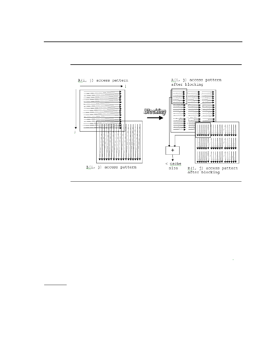
3-28
3
Intel Architecture Optimization Reference Manual
As one can see, all the redundant cache misses can be eliminated by
applying this loop blocking technique. If MAX is huge, loop blocking can
also help reduce the penalty from DTLB (data translation look-ahead
buffer) misses. In addition to improving the cache/memory performance,
this optimization technique also saves external bus bandwidth.
Tuning the Final Application
The best way to tune your application once it is functioning correctly is to
use a profiler that measures the application while it is running on a system.
Intel’s VTune analyzer can help you determine where to make changes in
your application to improve performance. Using the VTune analyzer can
help you with various phases required for optimized performance. See
Figure 3-3
Loop Blocking Access Pattern

Coding for SIMD Architectures
3
3-29
“VTune™ Performance Analyzer” in Chapter 7
for more details on using
the VTune analyzer. After every effort to optimize, you should check the
performance gains to see where you are making your major optimization
gains.


4-1
Using
SIMD Integer Instructions
4
The SIMD integer instructions provide performance improvements in
applications that are integer-intensive and can take advantage of the SIMD
architecture of Pentium
®
II and Pentium
III
processors.
The guidelines for using these instructions in addition to the guidelines
described in Chapter 2, “
General Optimization Guidelines
” will help
develop fast and efficient code that scales well across all processors with
MMX™ technology, as well as the Pentium II and Pentium
III
processors
that use Streaming SIMD Extensions with the new SIMD integer
instructions.
General Rules on SIMD Integer Code
The overall rules and suggestions are as follows:
•
Do not intermix MMX instructions, new SIMD integer instructions,
and floating-point instructions. See
Floating-Point, and MMX™ Technology Instructions”
section.
•
All optimization rules and guidelines described in Chapters 2 and 3 that
apply to both Pentium II and Pentium
III
processors using the new
SIMD integer instructions.

4-2
4
Intel Architecture Optimization Reference Manual
Planning Considerations
The planning considerations discussed in
Conversion to SIMD Programming”
in Chapter 3, apply when considering
using the new SIMD integer instructions available with the Streaming
SIMD Extensions.
Applications that benefit from these new instructions include video
encoding and decoding, as well as speech processing. Many existing
applications may also benefit from some of these new instructions,
particularly if they use MMX technology.
Review the planning considerations in the cited above section in Chapter 3
to determine if an application is computationally integer-intensive and can
take advantage of the SIMD architecture. If any of the considerations
discussed in Chapter 3 apply, the application is a candidate for performance
improvements using the new Pentium
III
processor SIMD integer
instructions, or MMX technology.
CPUID Usage for Detection of Pentium
®
III Processor
SIMD Integer Instructions
Applications must be able to determine if Streaming SIMD Extensions are
available. Follow the guidelines outlined in section
Processor Support of Streaming SIMD Extensions and MMX™
Technology”
in Chapter 3 to identify whether a system (processor and
operating system) supports the Streaming SIMD Extensions.
Using SIMD Integer, Floating-Point, and MMX™
Technology Instructions
The same rules and considerations for mixing MMX technology and
floating-point instructions apply for Pentium
III
processor SIMD integer
instructions. The Pentium
III
processor SIMD integer instructions use the
MMX technology registers, which are mapped onto the floating-point
registers. Thus, mixing Pentium
III
processor SIMD integer or MMX

Using SIMD Integer Instructions
4
4-3
instructions with floating-point instructions is not recommended.
Pentium
III
processor SIMD integer and MMX instructions, however, can
be intermixed with no transition required.
Using the EMMS Instruction
When generating MMX technology code, keep in mind that the eight MMX
technology registers are aliased on the floating-point registers. Switching
from MMX instructions to floating-point instructions can take up to fifty
clock cycles, so it is the best to minimize switching between these
instruction types. But when you need to switch, you need to use a special
instruction known as the
emms
instruction.
Using
emms
is like emptying a container to accommodate new content. For
example, MMX instructions automatically enable a tag word in the register
to validate the use of the
__m64
datatype. This validation resets the FP
register to enable its alias as an MMX technology register. To enable an FP
instruction again, reset the register state with the
emms
instruction
_m_empty()
as illustrated in Figure 4-1.
4-4
4
Intel Architecture Optimization Reference Manual
Figure 4-1
Using EMMS to Reset the Tag after an MMX Instruction
CAUTION.
Failure to reset the tag word for FP instructions after using
an MMX instruction can result in faulty execution or poor performance.
...
...
0
63
MM0
...
...
MM7
FP Tag
0
1
mmx
Registers
Clear Tag Word
with EMMS
_mm_empty()
.
.
.
.
.
.
...
...
0
79
FP0
...
...
FP7
FP Tag
0
1
FP Registers
.
.
.
.
.
.
FP Tag Word Aliases FP Registers to Act Like
mmx
Registers to Accept
_ _m64
Data Types
MMX Instruction Registers Need
_ _m64
Data types
FP Instruction Registers Need to be Reset to Accept
FP Data Types of 32, 64, and 80 bits
_mm_empty()
Clears the FP Tag Word and Allows FP Data Types in Registers
Again

Using SIMD Integer Instructions
4
4-5
Guidelines for Using EMMS Instruction
When writing an application that uses both floating-point and MMX
instructions, use the following guidelines to help you determine when to use
emms
:
•
If next instruction is FP—Use
_mm_empty()
after an MMX
instruction if the next instruction is an FP instruction; for example,
before doing calculations on floats, doubles or long doubles.
•
Don’t empty when already empty—If the next instruction uses an MMX
register,
_mm_empty()
incurs an operation with no benefit (no-op).
•
Group Instructions—Use different functions for regions that use FP
instructions and those that use MMX instructions. This eliminates
needing an EMMS instruction within the body of a critical loop.
•
Runtime initialization—Use
_mm_empty()
during runtime
initialization of
__m64
and FP data types. This ensures resetting the
register between data type transitions. See Example 4-1 for coding
usage.
Example 4-1 Resetting the Register between __m64 and FP Data Types
Incorrect Usage
Correct Usage
__m64 x = _m_paddd(y, z); __m64 x = _m_paddd(y, z);
float f = init();
float f = (_mm_empty(), init());
_____________________________________________________________
Further, you must be aware of the following situations when your code
generates an MMX instruction which uses the MMX technology registers
with the Intel C/C++ Compiler:
•
when using an MMX technology intrinsic
•
when using a Streaming SIMD Extension (for those intrinsics that use
MMX technology data)
•
when using an MMX instruction through inline assembly
•
when referencing an
__m64
data type variable

4-6
4
Intel Architecture Optimization Reference Manual
When developing code with both floating-point and MMX instructions,
follow these steps:
1.
Always call the
emms
instruction at the end of MMX technology code
when the code transitions to x87 floating-point code.
2.
Insert this instruction at the end of all MMX technology code segments
to avoid an overflow exception in the floating-point stack when a
floating-point instruction is executed.
3.
Use the
emms
instruction to clear the MMX technology registers and
set the value of the floating-point tag word to empty (that is, all ones).
Since the Pentium
III
processor SIMD integer instructions use the
MMX technology registers, which are aliased on the floating-point
registers, it is critical to clear the MMX technology registers before
issuing a floating-point instruction.
The
emms
instruction does not need to be executed when transitioning
between SIMD floating-point and MMX technology or Streaming SIMD
Extensions SIMD integer instructions or
x87
floating-point instructions.
Additional information on the floating-point programming model can be
found in the Pentium Processor Family Developer’s Manual, Volume 3,
Architecture and Programming, order number 241430. For more
documentation on
emms
, visit the
http://developer.intel.com
web site.
Data Alignment
Make sure your data is 16-byte aligned. Refer to section
for information on both Pentium II and Pentium
III
processors. Review this information to evaluate your data. If the data is
known to be unaligned, use
movups
(move unaligned packed single
precision) to avoid a general protection exception if
movaps
is used.
SIMD Integer and SIMD Floating-point Instructions
SIMD integer instructions and SIMD gloating-point instructions can be
intermixed with some restrictions. These restrictions result from their
respective port assignments. Port assignments are shown in Appendix C.
The port assignments for the relevant instructions are shown in Table 4-1.

Using SIMD Integer Instructions
4
4-7
SIMD Instruction Port Assignments
All the above instructions incur one µop with the exception of
psadw
, which
incurs three µops, and
pinsrw
, which incurs two µops. Note that some
instructions, such as
pmin
and
pmax
, can execute on both ports.
These instructions can be intermixed with the SIMD floating-point
instructions. Since the SIMD floating-point instructions are two µops,
intermix those with different port assignments from the current instruction
(see Appendix C, “
Instruction to Decoder Specification
”).
Coding Techniques for MMX Technology SIMD Integer
Instructions
This section contains several simple examples that will help you to get
started with coding your application. The goal is to provide simple,
low-level operations that are frequently used. The examples use a minimum
number of instructions necessary to achieve best performance on the
Pentium, Pentium Pro, Pentium II, and Pentium
III
processors.
Each example includes a short description, sample code, and notes if
necessary. These examples do not address scheduling as it is assumed the
examples will be incorporated in longer code sequences.
Table 4-1
Port Assignments
Port 0
Port 1
pmulhuw
pmin
pmax
psadw
pavgw
pshufw
pextrw
pinsrw
pmin
pmax
pmovmskb
psadw
pavgw

4-8
4
Intel Architecture Optimization Reference Manual
Unsigned Unpack
The MMX technology provides several instructions that are used to pack
and unpack data in the MMX technology registers. The unpack instructions
can be used to zero-extend an unsigned number. Example 4-2 assumes the
source is a packed-word (16-bit) data type.
Example 4-2 Unsigned Unpack Instructions
; Input: MM0
source value
; MM7 0
a local variable can be used
;
instead of the register MM7 if
;
desired.
; Output: MM0
two zero-extended 32-bit
;
doublewords from two low-end
;
words
;
MM1
two zero-extended 32-bit
;
doublewords from two high-end
;
words
movq
MM7, MM0 ; copy source
punpcklwd
MM0, MM7 ; unpack the 2 low-end words
; into two 32-bit doubleword
punpckhwd
MM1, MM7 ; unpack the 2 high-end words
; into two 32-bit doublewords
_____________________________________________________________
Signed Unpack
Signed numbers should be sign-extended when unpacking the values. This
is done differently than the zero-extend shown above. Example 4-3 assumes
the source is a packed-word (16-bit) data type.

Using SIMD Integer Instructions
4
4-9
Example 4-3 Signed Unpack Instructions
; Input:
MM0
source value
; Output: MM0
two sign-extended 32-bit
;
doublewords from the two low-end
;
words
;
;
MM1
two sign-extended 32-bit
;
doublewords from the two high-end
;
words
movq
MM1, MM0 ; copy source
punpckhwdMM1, MM0 ; unpack the 2 high-end words of the
; source into the second and fourth
; words of the destination
punpcklwdMM0, MM0 ; unpack the 2 low end words of the
; source into the second and fourth
; words of the destination
psrad
MM0, 16 ; sign-extend the 2 low-end words of
; the source into two 32-bit signed
; doublewords
psrad
MM1, 16 ; sign-extend the 2 high-end words
; of the source into two 32-bit
; signed doublewords
_____________________________________________________________
Interleaved Pack with Saturation
The pack instructions pack two values into the destination register in a
predetermined order. Specifically, the
packssdw
instruction packs two
signed doublewords from the source operand and two signed doublewords
from the destination operand into four signed words in the destination
register as shown in Figure 4-2.
4-10
4
Intel Architecture Optimization Reference Manual
Figure 4-3 illustrates two values interleaved in the destination register. The
two signed doublewords are used as source operands and the result is
interleaved signed words. The pack instructions can be performed with or
without saturation as needed.
Example 4-4 uses signed doublewords as source operands and the result is
interleaved signed words. The pack instructions can be performed with or
without saturation as needed.
Figure 4-2
PACKSSDW
mm, mm/mm64 Instruction Example
Figure 4-3
Interleaved Pack with Saturation
mm/m64
mm
mm
A
B
C
D
A
1
B
1
C
1
D
1
MM/M64
mm
mm
A
B
C
D
A
1
B
1
C
1
D
1

Using SIMD Integer Instructions
4
4-11
Example 4-4 Interleaved Pack with Saturation
; Input: MM0
signed source1 value
;
MM1 signed source2 value
; Output:MM0
the first and third words contain the
;
signed-saturated doublewords from MM0,
;
the second and fourth words contain
;
signed-saturated doublewords from MM1
packssdw
MM0, MM0 ; pack and sign saturate
packssdw
MM1, MM1 ; pack and sign saturate
punpcklwd
MM0, MM1 ; interleave the low-end 16-bit
; values of the operands
_____________________________________________________________
The pack instructions always assume that the source operands are signed
numbers. The result in the destination register is always defined by the pack
instruction that performs the operation. For example, the
packssdw
instruction packs each of the two signed 32-bit values of the two sources
into four saturated 16-bit signed values in the destination register. The
packuswb
instruction, on the other hand, packs each of the four signed
16-bit values of the two sources into four saturated eight-bit unsigned values
in the destination. A complete specification of the MMX instruction set can
be found in the Intel Architecture MMX Technology Programmer’s
Reference Manual, order number 243007.
Interleaved Pack without Saturation
Example 4-5 is similar to the last except that the resulting words are not
saturated. In addition, in order to protect against overflow, only the low
order 16 bits of each doubleword are used in this operation.
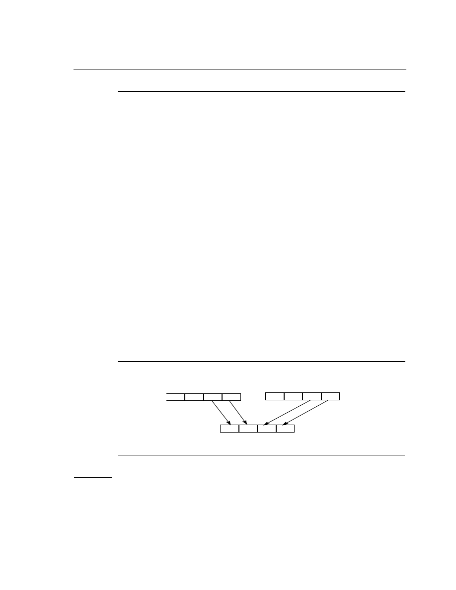
4-12
4
Intel Architecture Optimization Reference Manual
Example 4-5 Interleaved Pack without Saturation
; Input: MM0
signed source value
;
MM1
signed source value
; Output:MM0
the first and third words contain the
;
low 16-bits of the doublewords in MM0,
;
the second and fourth words contain the
;
low 16-bits of the doublewords in MM1
pslld MM1, 16 ; shift the 16 LSB from each of the
; doubleword values to the 16 MSB
; position
pand MM0, {0,ffff,0,ffff} ; mask to zero the 16 MSB
; of each doubleword value
por MM0, MM1
; merge the two operands
_____________________________________________________________
Non-Interleaved Unpack
The unpack instructions perform an interleave merge of
the data elements of
the destination and source operands into the destination register. The
following example merges the two operands into the destination registers
without interleaving. For example, take two adjacent elements of a
packed-word data type in
source1
and place this value in the low 32 bits of
the results. Then take two adjacent elements of a packed-word data type in
source2
and place this value in the high 32 bits of the results. One of the
destination registers will have the combination illustrated in Figure 4-4.
Figure 4-4
Result of Non-Interleaved Unpack in MM0
mm/m64
mm
1
3
1
0
1
2
1
1
2
3
2
0
2
2
2
1
2
1
1
0
2
0
1
1
mm
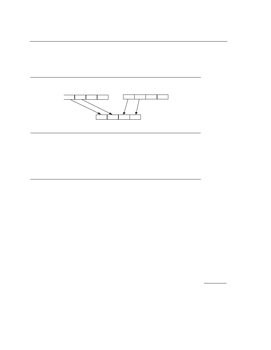
Using SIMD Integer Instructions
4
4-13
The other destination register will contain the opposite combination
illustrated in Figure 4-5.
Code in the Example 4-6 unpacks two packed-word sources in a
non-interleaved way. The goal is to use the instruction which unpacks
doublewords to a quadword, instead of using the instruction which unpacks
words to doublewords.
Example 4-6 Unpacking Two Packed-word Sources in a Non-interleaved Way
; Input:
MM0 packed-word source value
;
MM1 packed-word source value
; Output: MM0
contains the two low-end words of the
;
original sources, non-interleaved
;
MM2
contains the two high end words of the
;
original sources, non-interleaved.
movq
MM2, MM0 ; copy source1
punpckldq MM0, MM1 ; replace the two high-end words
; of MMO with two low-end words of
; MM1; leave the two low-end words
; of MM0 in place
punpckhdq MM2, MM1 ; move two high-end words of MM2
; to the two low-end words of MM2;
; place the two high-end words of
; MM1 in two high-end words of MM2
_____________________________________________________________
Figure 4-5
Result of Non-Interleaved Unpack in MM1
mm/m64
mm
1
3
1
0
1
2
1
1
2
3
2
0
2
2
2
1
2
3
1
2
2
2
1
3
mm

4-14
4
Intel Architecture Optimization Reference Manual
Complex Multiply by a Constant
Complex multiplication is an operation which requires four multiplications
and two additions. This is exactly how the
pmaddwd
instruction operates. In
order to use this instruction, you need to format the data into four 16-bit
values. The real and imaginary components should be 16-bits each.
Consider Example 4-7:
•
Let the input data be
Dr
and
Di
where
Dr
is real component of the data
and
Di
is imaginary component of the data.
•
Format the constant complex coefficients in memory as four 16-bit
values [
Cr -Ci Cr
]. Remember to load the values into the MMX
technology register using a
movq
instruction.
•
The real component of the complex product is
Pr = Dr*Cr - Di*Ci
and the imaginary component of the complex product is
Pi = Dr*Ci + Di*Cr
.
Example 4-7 Complex Multiply by a Constant
; Input:
MM0 complex value, Dr, Di
;
MM1 constant complex coefficient in the form
;
[Cr -Ci Cr]
; Output: MM0
two 32-bit dwords containing [Pr Pi]
punpckldq
MM0, MM0 ; makes [Dr Di Dr Di]
pmaddwd
MM0, MM1 ; done, the result is
; [(Dr*Cr-Di*Ci)(Dr*Ci+Di*Cr)]
_____________________________________________________________
Note that the output is a packed doubleword. If needed, a pack instruction
can be used to convert the result to 16-bit (thereby matching the format of
the input).
Absolute Difference of Unsigned Numbers
Example 4-8 computes the absolute difference of two unsigned numbers. It
assumes an unsigned packed-byte data type. Here, we make use of the
subtract instruction with unsigned saturation. This instruction receives

Using SIMD Integer Instructions
4
4-15
UNSIGNED
operands and subtracts them with
UNSIGNED
saturation. This
support exists only for packed bytes and packed words, not for packed
dwords.
Example 4-8 Absolute Difference of Two Unsigned Numbers
; Input:
MM0 source operand
;
MM1 source operand
; Output: MM0
absolute difference of the unsigned
;
operands
movq
MM2, MM0 ; make a copy of MM0
psubusb MM0, MM1 ; compute difference one way
psubusb MM1, MM2 ; compute difference the other way
por
MM0, MM1 ; OR them together
_____________________________________________________________
This example will not work if the operands are signed.
Absolute Difference of Signed Numbers
Example 4-9 computes the absolute difference of two signed numbers.
The technique used here is to first sort the corresponding elements of the
input operands into packed-words of the maximum values, and
packed-words of the minimum values. Then the minimum values are
subtracted from the maximum values to generate the required absolute
difference. The key is a fast sorting technique that uses the fact that
B = xor(A, xor(A,B))
and
A = xor(A,0)
. Thus in a packed data
type, having some elements being
xor(A,B)
and some being 0, you could
xor
such an operand with
A
and receive in some places values of
A
and in
some values of
B
. The following examples assume a packed-word data type,
each element being a signed value.
NOTE.
There is no MMX technology subtract instruction that receives
SIGNED
operands and subtracts them with
UNSIGNED
saturation.

4-16
4
Intel Architecture Optimization Reference Manual
Example 4-9 Absolute Difference of Signed Numbers
; Input:
MM0 signed source operand
;
MM1 signed source operand
;Output:
MM0
absolute difference of the unsigned
;
operands
movq MM2, MM0 ; make a copy of source1 (A)
pcmpgtw MM0, MM1 ; create mask of source1>source2
(A>B)
movq MM4, MM2 ; make another copy of A
pxor MM2, MM1 ; create the intermediate value of
; the swap operation - xor(A,B)
pand MM2, MM0 ; create a mask of 0s and xor(A,B)
; elements. Where A>B there will
; be a value xor(A,B) and where
; A<=B there will be 0.
pxor MM4, MM2 ; minima-xor(A,swap mask)
pxor MM1, MM3 ; maxima-xor(B, swap mask)
psubw MM1, MM4 ; absolute difference =
; maxima-minima
_____________________________________________________________

Using SIMD Integer Instructions
4
4-17
Absolute Value
Use Example 4-10 to compute
|
x
|
, where
x
is signed. This example
assumes signed words to be the operands.
Example 4-10 Computing Absolute Value
; Input:
MM0 signed source operand
; Output: MM1
ABS(MMO)
movq
MM1, MM0 ; make a copy of x
psraw
MM0,15
; replicate sign bit (use 31 if doing
; DWORDS)
pxor
MM0, MM1 ; take 1’s complement of just the
; negative fields
psubs
MM1, MM0 ; add 1 to just the negative fields
_____________________________________________________________
Clipping to an Arbitrary Signed Range [high, low]
This section explains how to clip a signed value to the signed range [
high,
low
]. Specifically, if the value is less than
low
or greater than
high
then
clip to
low
or
high,
respectively. This technique uses the packed-add and
packed-subtract instructions with unsigned saturation, which means that
this technique can only be used on packed-byte and packed-word data types.
CAUTION.
The absolute value of the most negative number (that is,
8000 hex for 16-bit) does not fit, but this code suggests what is possible
to do for this case: it gives
0x7fff
which is off by one.

4-18
4
Intel Architecture Optimization Reference Manual
Example 4-11 and Example 4-12 in this section use the constants
packed_max
and
packed_min
and show operations on word values. For
simplicity we use the following constants (corresponding constants are used
in case the operation is done on byte values):
•
packed_max
equals
0x7fff7fff7fff7fff
•
packed_min
equals
0x8000800080008000
•
packedD_low
contains the value
low
in all four words of the
packed-words data type
•
packed_high
contains the value
high
in all four words of the
packed-words data type
•
packed_usmax
all values equal
1
•
high_us
adds the
high
value to all data elements (4 words) of
packed_min
•
low_us
adds the
low
value to all data elements (4 words) of
packed_min
Example 4-11 Clipping to an Arbitrary Signed Range [high, low]
; Input:
MM0 signed source operands
; Output: MM1
signed operands clipped to the unsigned
;
range [high, low]
padd MM0, packed_min ; add with no saturation
; 0x8000 to convert to unsigned
paddusw MM0, (packed_usmax - high_us)
; in effect this clips to high
psubusw MM0, (packed_usmax - high_us + low_us)
; in effect this clips to low
paddw MM0, packed_low ; undo the previous two offsets
_____________________________________________________________
The code above converts values to unsigned numbers first and then clips
them to an unsigned range. The last instruction converts the data back to
signed data and places the data within the signed range. Conversion to
unsigned data is required for correct results when (
high
-
low
)
<
0x8000
.

Using SIMD Integer Instructions
4
4-19
If (
high
-
low
)
>= 0x8000
, the algorithm can be simplified as shown in
Example 4-12 Simplified Clipping to an Arbitrary Signed Range
; Input:
MM0 signed source operands
; Output: MM1
signed operands clipped to the unsigned
;
range [high, low]
paddssw MM0, (packed_max - packed_high)
; in effect this clips to high
psubssw MM0, (packed_usmax - packed_high +
packed_ow);
; clips to low
paddw MM0, low ; undo the previous two offsets
_____________________________________________________________
This algorithm saves a cycle when it is known that (
high
-
low
)
>=
0x8000
. The three-instruction algorithm does not work when (
high
-
low
)
< 0x8000
, because
0xffff
minus any number
< 0x8000
will yield a
number greater in magnitude than
0x8000
, which is a negative number.
When the second instruction,
psubssw MM0, (0xffff - high + low)
,
in the three-step algorithm (Example 4-12) is executed, a negative number is
subtracted. The result of this subtraction causes the values in
MM0
to be
increased instead of decreased, as should be the case, and an incorrect
answer is generated.
Clipping to an Arbitrary Unsigned Range [high, low]
The code in Example 4-13 clips an unsigned value to the unsigned range
[
high, low
]. If the value is less than
low
or greater than
high
, then clip
to
low
or
high
, respectively. This technique uses the packed-add and
packed-subtract instructions with unsigned saturation, thus this technique
can only be used on packed-bytes and packed-words data types.
The example illustrates the operation on word values.

4-20
4
Intel Architecture Optimization Reference Manual
Example 4-13 Clipping to an Arbitrary Unsigned Range [high, low]
; Input:
MM0 unsigned source operands
;Output:
MM1
unsigned operands clipped to the unsigned
;
range [HIGH, LOW] //
paddusw
MM0, 0xffff - high
; in effect this clips to high
psubusw
MM0, (0xffff - high + low)
; in effect this clips to low
paddw
MM0, low
; undo the previous two offsets
_____________________________________________________________
Generating Constants
The MMX instruction set does not have an instruction that will load
immediate constants to MMX technology registers. The following code
segments generate frequently used constants in an MMX technology
register. Of course, you can also put constants as local variables in memory,
but when doing so be sure to duplicate the values in memory and load the
values with a
movq
instruction, see Example 4-14.
Example 4-14 Generating Constants
pxor
MM0, MM0 ; generate a zero register in
MM0
pcmpeq MM1, MM1 ; Generate all 1’s in register MM1,
; which is -1 in each of the packed
; data type fields
pxor
MM0, MM0
pcmpeq MM1, MM1
psubb
MM0, MM1 [psubb MM0, MM1] (psubd MM0, MM1)
continued

Using SIMD Integer Instructions
4
4-21
Coding Techniques for Integer Streaming SIMD
Extensions
This section contains examples of the new SIMD integer instructions. Each
example includes a short description, sample code, and notes where
necessary.
These short examples, which usually are incorporated in longer code
sequences, do not address scheduling.
; three instructions above generate
; the constant 1 in every
; packed-byte [or packed-word]
; (or packed-dword) field
pcmpeq MM1, MM1
psrlw
MM1, 16-n
(psrld MM1, 32-n)
; two instructions above generate
; the signed constant 2
n–1
in every
; packed-word (or packed-dword) field
pcmpeq
MM1, MM1
psllw
MM1, n
(pslldMM1, n)
; two instructions above generate
; the signed constant -2
n
in every
; packed-word (or packed-dword) field
NOTE.
Because the MMX instruction set does not support shift
instructions for bytes,
2
n–1
and
-2
n
are relevant only for packed words
and packed dwords.
Example 4-14 Generating Constants (continued)
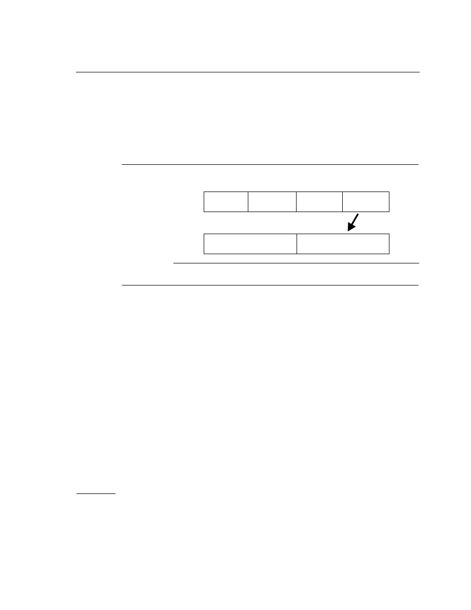
4-22
4
Intel Architecture Optimization Reference Manual
Extract Word
The
pextrw
instruction takes the word in the designated MMX technology
register selected by the two least significant bits of the immediate value and
moves it to the lower half of a 32-bit integer register, see Figure 4-6 and
Example 4-15.
Example 4-15 pextrw Instruction Code
; Input: eax source value immediate value:“0”
; Output: edx 32-bit integer register containing the
extracted word in the low-order bits & the
high-order bits zero-extended
movq mm0, [eax]
pextrw edx, mm0, 0
_____________________________________________________________
Insert Word
The
pinsrw
instruction loads a word from the lower half of a 32-bit integer
register or from memory and inserts it in the MMX technology destination
register at a position defined by the two least significant bits of the
immediate constant. Insertion is done in such a way that the three other
words from the destination register are left untouched, see Figure 4-7 and
Example 4-16.
Figure 4-6
pextrw Instruction
0
0
31
63
0..0
X1
X1
X2
X3
X4
MM
R32
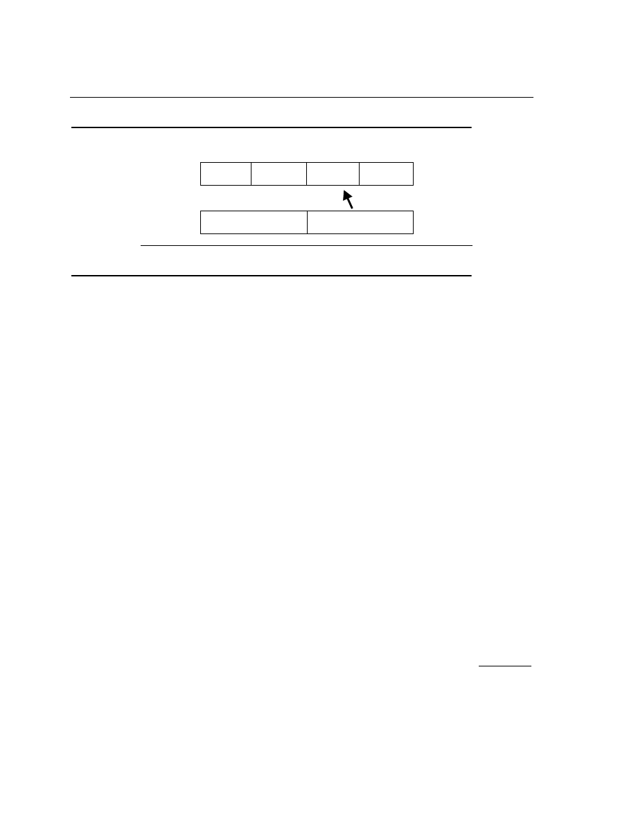
Using SIMD Integer Instructions
4
4-23
Example 4-16 pinsrw Instruction Code
; Input:
32-bit integer register: source value
immediate value: “1”.
; Output:
MMX technology register with new 16-bit
value inserted
movq mm0, [edx]
pinsrw mm0, eax, 1
_____________________________________________________________
Packed Signed Integer Word Maximum
The
pmaxsw
instruction returns the maximum between the four signed
words in either two MMX technology registers, or one MMX technology
register and a 64-bit memory location.
Packed Unsigned Integer Byte Maximum
The
pmaxub
instruction returns the maximum between the eight unsigned
bytes in either two MMX technology registers, or one MMX technology
register and a 64-bit memory location.
Packed Signed Integer Word Minimum
The
pminsw
instruction returns the minimum between the four signed
words in either two MMX technology registers, or one MMX technology
register and a 64-bit memory location.
Figure 4-7
pinsrw Instruction
0
0
31
63
X1
Y1
Y2
Y1
X3
X4
MM
R32
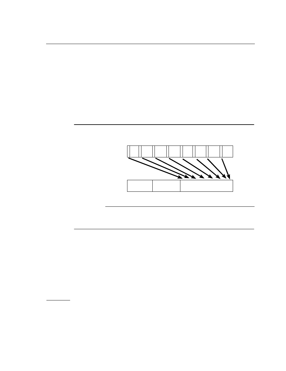
4-24
4
Intel Architecture Optimization Reference Manual
Packed Unsigned Integer Byte Minimum
The
pminub
instruction returns the minimum between the eight unsigned
bytes in either two MMX technology registers, or one MMX technology
register and a 64-bit memory location.
Move Byte Mask to Integer
The
pmovmskb
instruction returns an 8-bit mask formed from the most
significant bits of each byte of its source operand, see Figure 4-8 and
Example 4-17.
Example 4-17 pmovmskb Instruction Code
; Input:
source value
; Output:
32-bit register containing the byte mask
in the lower eight bits
movq mm0, [edi]
pmovmskb eax, mm0
_____________________________________________________________
Figure 4-8
pmovmskb Instruction Example
0
0
31
63
0..0
0..0
7
15
23
31
39
47
55
7
MM
R32

Using SIMD Integer Instructions
4
4-25
Packed Multiply High Unsigned
The
pmulhuw
instruction multiplies the four unsigned words in the
destination operand with the four unsigned words in the source operand.
The high-order 16 bits of the 32-bit immediate results are written to the
destination operand.
Packed Shuffle Word
The
pshuf
instruction (see Figure 4-9, Example 4-18) uses the immediate
(
imm8
) operand to select between the four words in either two MMX
technology registers or one MMX technology register and a 64-bit memory
location. Bits 1 and 0 of the immediate value encode the source for
destination word 0 (
MMX[15-0]
), and so on as shown in the table:
Bits 7 and 6 encode for word 3 (
MMX[63-48]
). Similarly, the 2-bit
encoding represents which source word is used, for example, binary
encoding of 10 indicates that source word 2 (
MM2/mem[47-32]
) is used,
see Example 4-18 and Example 4-18.
Bits
Word
1 - 0
0
3 - 2
1
5 - 4
2
7 - 6
3
Figure 4-9
pshuf Instruction Example
0
63
X1
X1
X2
X2
X3
X3
X4
X4
0
63
MM/m64
MM
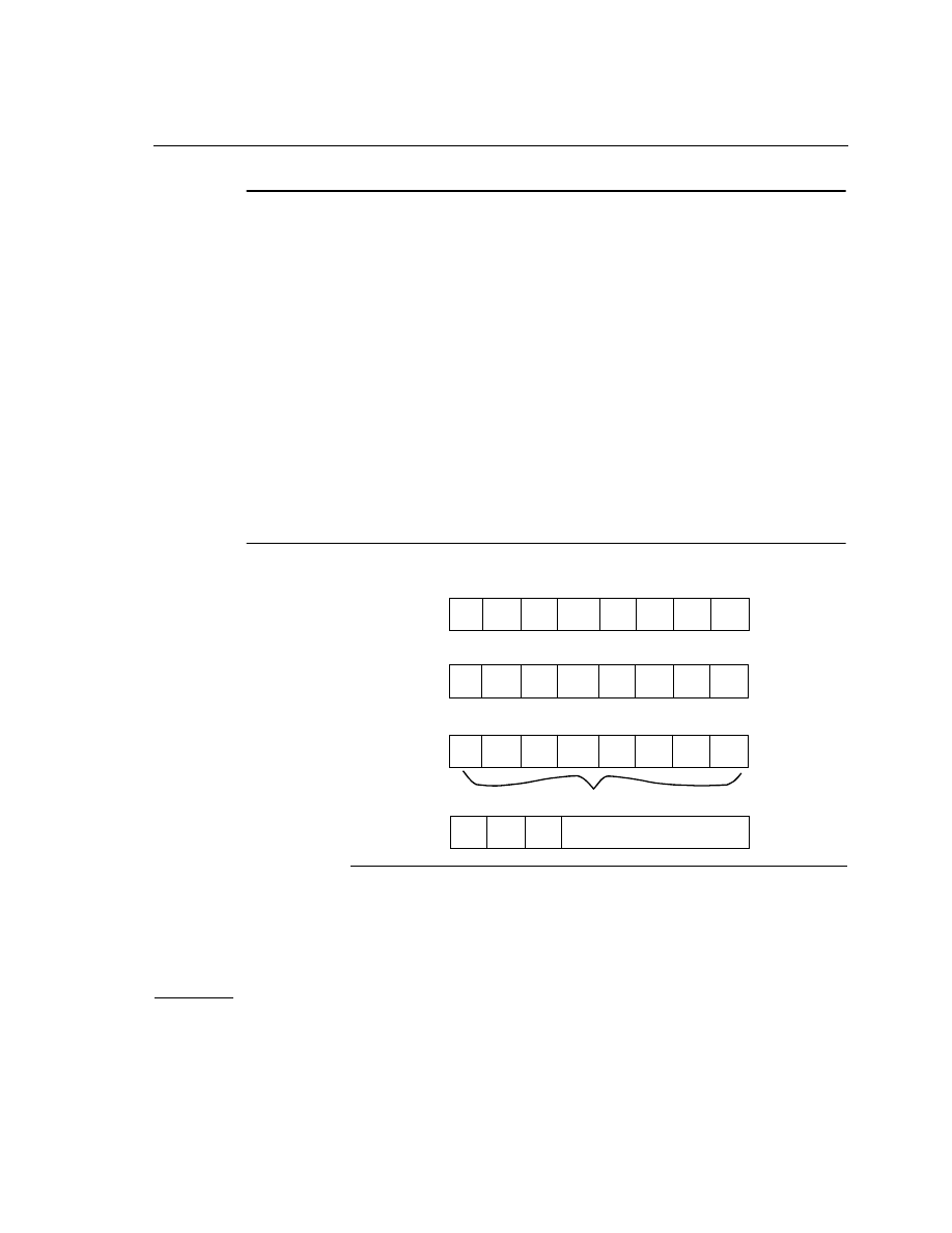
4-26
4
Intel Architecture Optimization Reference Manual
Example 4-18 pshuf Instruction Code
; Input: edi source value
; Output: MM1 MM register containing the byte mask in
the lower eight bits
movq mm0, [edi]
pshufw mm1, mm0, 0x1b
_____________________________________________________________
Packed Sum of Absolute Differences
The
PSADBW
instruction (see Figure 4-10) computes the absolute value of
the difference of unsigned bytes for either two MMX technology registers,
or one MMX technology register and a 64-bit memory location. These
differences are then summed to produce a word result in the lower 16-bit
field, and the upper three words are set to zero.
Figure 4-10
PSADBW Instruction Example
0
0
0
63
63
63
X1
Y1
T1
X2
Y2
T2
X3
Y3
T3
X4
Y4
T4
X8
Y8
T8
X7
Y7
T7
X6
Y6
T6
X5
Y5
T5
0
63
15
31
47
MM/m64
MM
MM
0..0 0..0 0..0
-
-
-
-
-
-
-
-
=
=
=
=
=
=
=
=
Te m p
T1+T2+T3+T4+T5+T6+t7+T8

Using SIMD Integer Instructions
4
4-27
The subtraction operation presented above is an absolute difference, that is,
t = abs(x-y
)
. The byte values are stored in temporary space, all values
are summed together, and the result is written into the lower word of the
destination register.
Packed Average (Byte/Word)
The
pavgb
and
pavgw
instructions add the unsigned data elements of the
source operand to the unsigned data elements of the destination register,
along with a carry-in. The results of the addition are then each
independently shifted to the right by one bit position. The high order bits of
each element are filled with the carry bits of the corresponding sum.
The destination operand is an MMX technology register. The source
operand can either be an MMX technology register or a 64-bit memory
operand.
The
PAVGB
instruction operates on packed unsigned bytes and the
PAVGW
instruction operates on packed unsigned words.
Memory Optimizations
You can improve memory accesses using the following techniques:
•
Partial Memory Accesses
•
Instruction Selection
•
Increasing Bandwidth of Memory Fills and Video Fills
•
Pre-fetching data with Streaming SIMD Extensions (see Chapter 6,
“
Optimizing Cache Utilization for Pentium® III Processors
The MMX technology registers allow you to move large quantities of data
without stalling the processor. Instead of loading single array values that are
8, 16, or 32 bits long, consider loading the values in a single quadword, then
incrementing the structure or array pointer accordingly.
Any data that will be manipulated by MMX instructions should be loaded
using either:
•
the MMX instruction that loads a 64-bit operand (for example,
movq
MM0
,
m64
)

4-28
4
Intel Architecture Optimization Reference Manual
•
the register-memory form of any MMX instruction that operates on a
quadword memory operand (for example,
pmaddw
MM0
,
m64
)
•
all SIMD data should be stored using the MMX instruction that stores a
64-bit operand (for example,
movq m64
,
MM0
)
The goal of these recommendations is twofold. First, the loading and storing
of SIMD data is more efficient using the larger quadword block sizes.
Second, this helps to avoid the mixing of 8-, 16-, or 32-bit load and store
operations with 64-bit MMX technology load and store operations to the
same SIMD data. This, in turn, prevents situations in which small loads
follow large stores to the same area of memory, or large loads follow small
stores to the same area of memory. Pentium II and Pentium
III
processors
stall in these situations.
Partial Memory Accesses
Let’s consider a case with large load after a series of small stores to the
same area of memory (beginning at memory address
mem
). The large load
will stall in this case as shown in Example 4-19.
Example 4-19 A Large Load after a Series of Small Stalls
mov
mem, eax ; store dword to address “mem"
mov
mem + 4, ebx ; store dword to address “mem + 4"
:
:
movq mm0, mem ; load qword at address “mem", stalls
_____________________________________________________________
The
movq
must wait for the stores to write memory before it can access all
the data it requires. This stall can also occur with other data types (for
example, when bytes or words are stored and then words or doublewords are
read from the same area of memory). When you change the code sequence
as shown in Example 4-20, the processor can access the data without delay.

Using SIMD Integer Instructions
4
4-29
Example 4-20 Accessing Data without Delay
movd
mm1, ebx
; build data into a qword first
; before storing it to memory
movd
mm2, eax
psllq
mm1, 32
por
mm1, mm2
movq
mem, mm1 ; store SIMD variable to “mem" as
; a qword
:
:
movq
mm0, mem
; load qword SIMD “mem", no stall
_____________________________________________________________
Let us now consider a case with a series of small loads after a large store to
the same area of memory (beginning at memory address
mem
). The small
loads will stall in this case as shown in Example 4-21.
Example 4-21 A Series of Small Loads after a Large Store
movq
mem, mm0 ; store qword to address “mem"
:
:
mov
bx, mem + 2 ; load word at “mem + 2" stalls
mov
cx, mem + 4; load word at “mem + 4" stalls
_____________________________________________________________
The word loads must wait for the quadword store to write to memory before
they can access the data they require. This stall can also occur with other
data types (for example, when doublewords or words are stored and then
words or bytes are read from the same area of memory). When you change
the code sequence as shown in Example 4-22, the processor can access the
data without delay.

4-30
4
Intel Architecture Optimization Reference Manual
Example 4-22 Eliminating Delay for a Series of Small Loads after a Large Store
movq
mem, mm0 ; store qword to address “mem"
:
:
movq
mm1, mem ; load qword at address “mem"
movd
eax, mm1
; transfer “mem + 2" to eax from
; MMX technology register, not
; memory
psrlq
mm1, 32
shr
eax, 16
movd
ebx, mm1
; transfer “mem + 4" to bx from
; MMX technology register, not
; memory
and
ebx, 0ffffh
____________________________________________________________
These transformations, in general, increase the number of instructions
required to perform the desired operation. For Pentium II and Pentium
III
processors, the performance penalty due to the increased number of
instructions is more than offset by the benefit.
Instruction Selection to Reduce Memory Access Hits
An MMX instruction may have two register operands (
OP reg, reg
) or
one register and one memory operand (
OP reg, mem
), where
OP
represents
the instruction opcode,
reg
represents the register, and
mem
represents
memory.
OP reg, mem
instructions are useful in some cases to reduce
register pressure, increase the number of operations per cycle, and reduce
code size.
The following discussion assumes that the memory operand is present in the
data cache. If it is not, then the resulting penalty is usually large enough to
obviate the scheduling effects discussed in this section.
In Pentium processors,
OP reg, mem
MMX instructions do not have
longer latency than
OP reg, reg
instructions (assuming a cache hit).
They do have more limited pairing opportunities, however. In Pentium II
and Pentium
III
processors,
OP
reg,
mem
MMX instructions translate into

Using SIMD Integer Instructions
4
4-31
two µops, as opposed to one µop for the
OP reg, reg
instructions. Thus,
they tend to limit decoding bandwidth and occupy more resources than
OP reg, reg
instructions.
Recommended usage of
OP reg, mem
instructions depends on whether the
MMX technology code is memory bound (that is, execution speed is limited
by memory accesses). Generally, an MMX technology code section is
considered to be memory-bound if the following inequality is true:
Instructions/2 < Memory Accesses + non-MMX Instructions/2
For memory-bound MMX technology code, the recommendation is to
merge loads whenever the same memory address is used more than once.
This reduces the number of memory accesses.
For example,
OP
MM0, [address A]
OP
MM1, [address A]
becomes
movq MM2, [address A]
OP
MM0, MM2
OP MM1, MM2
For MMX technology code that is not memory-bound, load merging is
recommended only if the same memory address is used more than twice.
Where load merging is not possible, usage of
OP reg, mem
instructions is
recommended to minimize instruction count and code size.
For example,
movq MM0, [address A]
OP
MM1, MM0
becomes
OP
MM1, [address A]
In many cases, a
movq reg,
reg
and
OP reg,
mem
can be replaced by a
movq reg,
mem
and
OP reg,
reg
. This should be done where possible,
since it saves one µop on Pentium II and Pentium
III
processors.

4-32
4
Intel Architecture Optimization Reference Manual
The code below, where OP is a commutative operation,
movq MM1, MM0
(1 µop)
OP
MM1, [address A]
(2 µops)
becomes:
movq MM1, [address A] (1 µop)
OP
MM1, MM0
(1 µop)
Increasing Bandwidth of Memory Fills and Video Fills
It is beneficial to understand how memory is accessed and filled. A
memory-to-memory fill (for example a memory-to-video fill) is defined as a
32-byte (cache line) load from memory which is immediately stored back to
memory (such as a video frame buffer). The following are guidelines for
obtaining higher bandwidth and shorter latencies for sequential memory
fills (video fills). These recommendations are relevant for all Intel
®
architecture processors with MMX technology and refer to cases in which
the loads and stores do not hit in the second level cache.
Increasing Memory Bandwidth Using the MOVQ Instruction
Loading any value will cause an entire cache line to be loaded into the
on-chip cache. But using
movq
to store the data back to memory instead of
using 32-bit stores (for example,
movd
) will reduce by half the number of
stores per memory fill cycle. As a result, the bandwidth of the memory fill
cycle increases significantly. On some Pentium processor-based systems,
30% higher bandwidth was measured when 64-bit stores were used instead
of 32-bit stores. Additionally, on Pentium II and Pentium
III
processors, this
avoids a partial memory access when both the loads and stores are done
with the
MOVQ
instruction.
Also, intermixing reads and writes is slower than doing a series of reads
then writing out the data. For example when moving memory, it is faster to
read several lines into the cache from memory then write them out again to
the new memory location, instead of issuing one read and one write.
Increasing Memory Bandwidth by Loading and Storing to
and from the Same DRAM Page
DRAM is divided into pages, which are not the same as operating system
(OS) pages. The size of a DRAM page is a function of the total size of the
DRAM and the organization of the DRAM. Page sizes of several Kbytes are

Using SIMD Integer Instructions
4
4-33
common. Like OS pages, DRAM pages are constructed of sequential
addresses. Sequential memory accesses to the same DRAM page have
shorter latencies than sequential accesses to different DRAM pages. In
many systems the latency for a page miss (that is, an access to a different
page instead of the page previously accessed) can be twice as large as the
latency of a memory page hit (access to the same page as the previous
access). Therefore, if the loads and stores of the memory fill cycle are to the
same DRAM page, a significant increase in the bandwidth of the memory
fill cycles can be achieved.
Increasing the Memory Fill Bandwidth by Using Aligned
STORES
Unaligned stores will double the number of stores to memory. Intel strongly
recommends that quadword stores be 8-byte aligned. Four aligned
quadword stores are required to write a cache line to memory. If the
quadword store is not 8-byte aligned, then two 32-bit writes result from
each
MOVQ
store instruction. On some systems, a 20% lower bandwidth was
measured when 64-bit misaligned stores were used instead of aligned
stores.
Use 64-Bit Stores to Increase the Bandwidth to Video
Although the PCI bus between the processor and the frame buffer is 32 bits
wide, using
movq
to store to video is faster on most Pentium
processor-based systems than using twice as many 32-bit stores to video.
This occurs because the bandwidth to PCI write buffers (which are located
between the processor and the PCI bus) is higher when quadword stores are
used.
Increase the Bandwidth to Video Using Aligned Stores
When a nonaligned store is encountered, there is a dramatic decrease in the
bandwidth to video. Misalignment causes twice as many stores and the
latency of stores on the PCI bus (to the frame buffer) is much longer. On the
PCI bus, it is not possible to burst sequential misaligned stores. On Pentium
processor-based systems, a decrease of 80% in the video fill bandwidth is
typical when misaligned stores are used instead of aligned stores.

4-34
4
Intel Architecture Optimization Reference Manual
Scheduling for the SIMD Integer Instructions
Scheduling instructions affects performance because the latency of
instructions affects other instructions acting on them.
Scheduling Rules
All MMX instructions can be pipelined, including the multiply instructions
on Pentium II and Pentium
III
processors. All instructions take a single
clock to execute except MMX technology multiply instructions which take
three clocks.
Since multiply instructions take three clocks to execute, the result of a
multiply instruction can be used only by other instructions issued three
clocks later. For this reason, avoid scheduling a dependent instruction in the
two-instruction sequences following the multiply.
The store of a register after writing the register must wait for two clock
cycles after the update of the register. Scheduling the store of at least two
clock cycles after the update avoids a pipeline stall.

5-1
Optimizing
Floating-point Applications
5
This chapter discusses general rules for optimizing single-instruction,
multiple-data (SIMD) floating-point code and provides examples that
illustrate the optimization techniques for SIMD floating-point applications.
Rules and Suggestions
The rules and suggestions listed in this section help optimize floating-point
code containing SIMD floating-point instructions. Generally, it is important
to understand and balance port utilization to create efficient SIMD
floating-point code. The basic rules and suggestions include the following:
•
Balance the limitations of the architecture.
•
Schedule instructions to resolve dependencies.
•
Schedule usage of the triple/quadruple rule (port 0, port 1, port 2, 3,
and 4).
•
Group instructions that use the same registers as closely as possible.
Take into consideration the resolution of true dependencies.
•
Intermix SIMD floating-point operations that use port 0 and port 1.
•
Do not issue consecutive instructions that use the same port.
•
Exceptions: mask exceptions to achieve higher performance.
Unmasked exceptions may cause a reduction in the retirement rate.
•
Utilize the flush-to-zero mode for higher performance to avoid the
penalty of dealing with denormals and underflows.
•
Incorporate the prefetch instruction whenever possible (for details,
refer to Chapter 6, “
Optimizing Cache Utilization for Pentium® III
” ).

5-2
5
Intel Architecture Optimization Reference Manual
•
Try to emulate conditional moves by using masked compares and
logicals instead of using conditional jumps.
•
Use MMX™ technology instructions if the computations can be done
in SIMD integer, for shuffling data, or for copying data that is not used
later in SIMD floating-point computations.
•
If the algorithm requires extended precision, then conversion to SIMD
floating-point code is not advised because the Streaming SIMD
Extensions for floating-point instructions are single-precision.
•
Use the reciprocal instructions followed by iteration for increased
accuracy. These instructions yield reduced accuracy but execute much
faster. Note the following:
— If reduced accuracy is acceptable, use them with no iteration.
— If near full accuracy is needed, use a Newton-Raphson iteration.
— If full accuracy is needed, then use divide and square root which
provide more accuracy, but slow down performance.
Planning Considerations
Whether adapting an existing application or creating a new one, using
SIMD floating-point instructions to optimal advantage requires
consideration of several issues. In general, when choosing candidates for
optimization, look for code segments that are computationally intensive and
floating-point intensive. Also consider efficient use of the cache
architecture. Intel provides tools for evaluation and tuning.
The sections that follow answer the questions that should be raised before
implementation:
•
Which part of the code benefits from SIMD floating-point instructions?
•
Is the current algorithm the most appropriate for SIMD floating-point
instructions?
•
Is the code floating-point intensive?
•
Is the data arranged for efficient utilization of the SIMD floating-point
registers?
•
Is this application targeted for processors without SIMD floating-point
instructions?

Optimizing Floating-point Applications
5
5-3
Which Part of the Code Benefits from SIMD Floating-point
Instructions?
Determine which code will benefit from SIMD floating-point instructions.
Floating-point intensive applications that repeatedly execute similar
operations where operations are repeated for multiple data sets, such as
loops, might benefit from using SIMD floating-point instructions. Other
factors that need to be considered include data organization if the kernel
operation can use parallelism.
If the algorithm employed requires performance, range, and precision, then
floating-point computation is the best choice. If performance is the primary
reason for floating-point implementation, then the algorithm could increase
its performance if converted to SIMD floating-point code.
MMX Technology and Streaming SIMD Extensions Floating-point
Code
When generating SIMD floating-point code, the rules for mixing MMX
technology code and floating-point code do not apply. Since the SIMD
floating-point registers are separate registers and are not mapped onto
existing registers, SIMD floating-point code can be mixed with
floating-point and MMX technology code. The SIMD floating-point
instructions map to the same ports as the MMX technology and
floating-point code. To avoid instruction stalls, consult Appendix C,
“
Instruction to Decoder Specification
,” when writing an application that
mixes these various codes.
Scalar Code Optimization
In terms of performance, the Streaming SIMD Extensions scalar code can
do as well as x87 but has the following advantages:
•
Using a flat register model rather than a stack model.
•
Mixing with MMX technology code without penalty.
•
Using scalar instructions on packed SIMD floating-point data when
needed, since they bypass the upper fields of the packed data. This
bypassing mechanism allows scalar code to have extra register storage
by using the upper fields for temporary storage.

5-4
5
Intel Architecture Optimization Reference Manual
The following are some additional points to take into consideration when
writing scalar code:
•
The scalar code can run on two execution ports in addition to the load
and store ports, an advantage over x87 code where it had only one
floating-point execution port.
•
The scalar code is decoded as 1 per cycle.
•
To increase performance while avoiding this decoder limitation, use
implicit loads with arithmetic instructions that increase the number of
µops decoded.
EMMS Instruction Usage Guidelines
The EMMS instruction sets the values of all the tags in the floating-point
unit (FPU) tag word to empty (all ones).
There are no requirements for using the
emms
instruction when mixing
SIMD floating-point code with either MMX technology code or
floating-point code. The
emms
instruction need only be used in the context
of the existing rules for MMX technology intrinsics and floating-point code.
It is only required when transitioning from MMX technology code to
floating-point code. See Table 5-1 for details.
Table 5-1
EMMS Instruction Usage Guidelines
Flow 1
Flow 2
EMMS
Required
x87
MMX technology
No; ensure that
stack is empty
x87
Streaming SIMD Extensions
No; ensure that
stack is empty
x87
Streaming SIMD Extensions-
SIMD floating-point
No
MMX technology
x87
Yes
MMX technology
Streaming SIMD Extensions-
SIMD integer
No
MMX technology
Streaming SIMD Extensions-
SIMD floating-point
No
continued

Optimizing Floating-point Applications
5
5-5
CPUID Usage for Detection of SIMD Floating-point Support
Applications must be able to determine if Streaming SIMD Extensions are
available. Please refer the section
“Checking for Processor Support of
Streaming SIMD Extensions and MMX™ Technology” in Chapter 3
for the
techniques to determine whether the processor and operating system
support Streaming SIMD Extensions.
Data Alignment
The data must be 16-byte-aligned for packed floating-point operations (that
is, no alignment constraint for scalar floating-point). If the data is not
16-byte-aligned, a general protection exception will be generated. If you
know that the data is not aligned, use the
movups
(
mov
unaligned)
instruction to avoid the protection error exception. The
movups
instruction
is the only one that can access unaligned data.
Streaming SIMD
Extensions-
SIMD integer
x87
Yes
Streaming SIMD
Extensions-
SIMD integer
MMX technology
No
Streaming SIMD
Extensions-
SIMD integer
Streaming SIMD Extensions-
SIMD floating-point
No
Streaming SIMD
Extensions-
SIMD floating-point
x87
No
Streaming SIMD
Extensions-
SIMD floating-point
MMX technology
No
Streaming SIMD
Extensions-
SIMD floating-point
Streaming SIMD Extensions-
SIMD integer
No
Table 5-1
EMMS Instruction Usage Guidelines (continued)
Flow 1
Flow 2
EMMS
Required

5-6
5
Intel Architecture Optimization Reference Manual
Accessing data that is properly aligned can save six to nine cycles on the
Pentium
®
III
processor. If the data is properly aligned on a 16-byte
boundary, frequent access can provide a significant performance
improvement.
Data Arrangement
Since the Streaming SIMD Extensions incorporate a SIMD architecture,
arranging the data to fully use the SIMD registers produces optimum
performance. This implies contiguous data for processing, which leads to
fewer cache misses and potentially quadruples the speed. These
performance gains occur because the four-element SIMD registers can be
loaded with 128-bit load instructions (
movaps
– move aligned packed
single precision).
Refer to the
“Stack and Data Alignment” in Chapter 3
for data arrangement
recommendations. Duplicating and padding techniques overcome the
misalignment problem that can occur in some data structures and
arrangements. This increases the data space but avoids the expensive
penalty for misaligned data access.
The traditional data arrangement does not lend itself to SIMD parallel
techniques in some applications. Traditional 3D data structures, for
example, do not lead to full utilization of the SIMD registers. This data
layout has traditionally been an array of structures (AoS). To fully utilize
the SIMD registers, a new data layout has been proposed—a structure of
arrays (SoA). The SoA structure allows the application to fully utilize the
SIMD registers. With full utilization comes more optimized performance.
Vertical versus Horizontal Computation
Traditional 3D data structures do not lend themselves to vertical
computation. The data can still be operated on and computation can
proceed, but without optimally utilizing the SIMD registers. To optimally
utilize the SIMD registers the data can be organized in the SoA format as
mentioned above.

Optimizing Floating-point Applications
5
5-7
Consider 3D geometry data organization. One way to apply SIMD
technology to a typical 3D geometry is to use horizontal execution. This
means to parallelize the computation on the
x
,
y
,
z
, and
w
components of a
single vertex (that is, of a single vector simultaneously referred to as an
xyz
data representation, see the diagram below).
Vertical computation, SoA, is recommended over horizontal, for several
reasons:
•
When computing on a single vector (
xyz
), it is common to use only a
subset of the vector components; for example, in 3D graphics the
W
component is sometimes ignored. This means that for single-vector
operations, 1 of 4 computation slots is not being utilized. This results in
a 25% reduction of peak efficiency, and only 75% peak performance
can be attained.
•
It may become difficult to hide long latency operations. For instance,
another common function in 3D graphics is normalization, which
requires the computation of a reciprocal square root (that is, 1/sqrt);
both the division and square root are long latency operations. With
vertical computation (SoA), each of the 4 computation slots in a SIMD
operation is producing a unique result, so the net latency per slot is L/4
where L is the overall latency of the operation. However, for horizontal
computation, the 4 computation slots each produce the same result,
hence to produce 4 separate results requires a net latency per slot of L.
How can the data be organized to utilize all 4 computation slots? The vertex
data can be reorganized to allow computation on each component of 4
separate vertices, that is, processing multiple vectors simultaneously. This
will also be referred to as an SoA form of representing vertices data shown
in Table 5-2.
Table 5-2
SoA Form of Representing Vertices Data
Vx array
X1
X2
X3
X4
.....
Xn
Vy array
Y1
Y2
Y3
Y4
.....
Yn
Vz array
Z1
Z2
Z3
Y4
.....
Zn
Vw array
W1
W2
W3
W4
.....
Wn
X
Y
Z
W
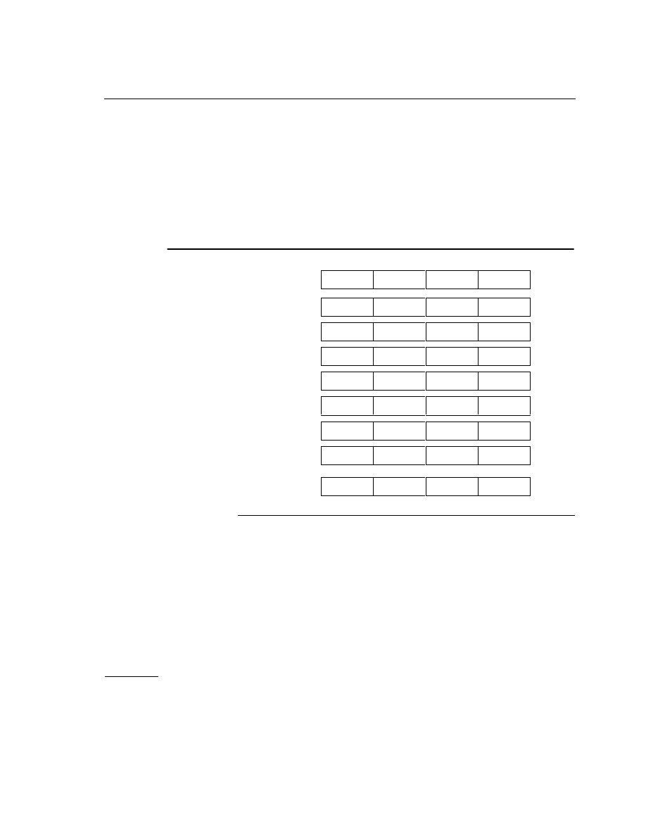
5-8
5
Intel Architecture Optimization Reference Manual
Organizing data in this manner yields a unique result for each
computational slot for each arithmetic operation. Vertical computation takes
advantage of the inherent parallelism in 3D geometry processing of vertices.
It assigns the computation of four vertices to the four compute slots of the
Pentium
III
processor, thereby eliminating the disadvantages of the
horizontal approach described earlier. The dot product operation
implements the SoA representation of vertices data. A schematic
representation of dot product operation is shown in Figure 5-1.
Example 5-1 shows how 1 result would be computed for 7 instructions if the
data were organized as AoS. Hence 4 results would require 28 instructions.
Figure 5-1
Dot Product Operation
X1
X2
X3
X4
x
Fx
Fx
Fx
Fx
+
Y1
Y2
Y3
Y4
x
Fy
Fy
Fy
Fy
+
Z1
Z2
Z3
Z4
x
Fz
Fz
Fz
Fz
+
W1
W2
W3
W4
x
Fw
Fw
Fw
Fw
=
R1
R2
R3
R4

Optimizing Floating-point Applications
5
5-9
Example 5-1 Pseudocode for Horizontal (xyz, AoS) Computation
mulps
; x*x’, y*y’, z*z’
movaps
; reg->reg move, since next steps overwrite
shufps
; get b,a,d,c from a,b,c,d
addps
; get a+b,a+b,c+d,c+d
movaps
; reg->reg move
shufps
; get c+d,c+d,a+b,a+b from prior addps
addps
; get a+b+c+d,a+b+c+d,a+b+c+d,a+b+c+d
_____________________________________________________________
Now consider the case when the data is organized as SoA. Example 5-2
demonstrates how 4 results are computed for 5 instructions.
Example 5-2 Pseudocode for Vertical (xxxx, yyyy, zzzz, SoA) Computation
mulps
; x*x’ for all 4 x-components of 4 vertices
mulps
; y*y’ for all 4 y-components of 4 vertices
mulps
; z*z’ for all 4 z-components of 4 vertices
addps
; x*x’ + y*y’
addps
; x*x’+y*y’+z*z’
_____________________________________________________________
For the most efficient use of the four component-wide registers,
reorganizing the data into the SoA format yields increased throughput and
hence much better performance for the instructions used.
As can be seen from this simple example, vertical computation yielded
100% use of the available SIMD registers and produced 4 results. If the data
structures are restricted to a format that is not “friendly to vertical
computation,” it can be rearranged “on the fly” to achieve full utilization of
the SIMD registers. This operation referred to as “swizzling” and the
“deswizzling” operation are discussed in the following sections.

5-10
5
Intel Architecture Optimization Reference Manual
Data Swizzling
In many algorithms, swizzling data from one format to another is required.
An example of this is AoS format, where the vertices come as
xyz
adjacent
coordinates. Rearranging them into SoA format,
xxxx
,
yyyy
,
zzzz
, allows
more efficient SIMD computations. The following instructions can be used
for efficient data shuffling and swizzling:
•
movlps
,
movhps
load/store and move data on half sections of the
registers
•
shuffps
,
unpackhps
, and
unpacklps
unpack data
To gather data from 4 different memory locations on the fly, follow steps:
1.
identify the first half of the 128-bit memory location.
2.
group the different halves together using the
movlps
and
movhps
to
form an
xyxy
layout in two registers
3.
from the 4 attached halves, get the
xxxx
by using one shuffle, the
yyyy
by using another shuffle.
The
zzzz
is derived the same way but only requires one shuffle.
Example 5-3 illustrates the swizzle function.
Example 5-3 Swizzling Data
typedef struct _VERTEX_AOS {
float x, y, z, color;
} Vertex_aos; // AoS structure declaration
typedef struct _VERTEX_SOA {
float x[4], float y[4], float z[4];
float color[4];
} Vertex_soa; // SoA structure declaration
void swizzle_asm (Vertex_aos *in, Vertex_soa *out)
{
// in mem: x1y1z1w1-x2y2z2w2-x3y3z3w3-x4y4z4w4-
// SWIZZLE XYZW --> XXXX
asm {
mov ecx, in // get structure addresses
mov edx, out
_____________________________________________________________
continued

Optimizing Floating-point Applications
5
5-11
Example 5-3 Swizzling Data (continued)
movlps xmm7, [ecx] // xmm7 = -- -- y1 x1
movhps xmm7, [ecx+16] // xmm7 = y2 x2 y1 x1
movlps xmm0, [ecx+32] // xmm0 = -- -- y3 x3
movhps xmm0, [ecx+48] // xmm0 = y4 x4 y3 x3
movaps xmm6, xmm7 // xmm6 = y1 x1 y1 x1
shufps xmm7, xmm0, 0x88// xmm7 = x1 x2 x3 x4 => X
shufps xmm6, xmm0, 0xDD// xmm6 = y1 y2 y3 y4 => Y
movlps xmm2, [ecx+8] // xmm2 = -- -- w1 z1
movhps xmm2, [ecx+24] // xmm2 = w2 z2 u1 z1
movlps xmm1, [ecx+40] // xmm1 = -- -- s3 z3
movhps xmm1, [ecx+56] // xmm1 = w4 z4 w3 z3
movaps xmm0, xmm2 // xmm0 = w1 z1 w1 z1
shufps xmm2, xmm1, 0x88// xmm2 = z1 z2 z3 z4 => Z
shufps xmm0, xmm1, 0xDD// xmm6 = w1 w2 w3 w4 => W
movaps [edx], xmm7 // store X
movaps [edx+16], xmm6 // store Y
movaps [edx+32], xmm2 // store Z
movaps [edx+48], xmm0 // store W
// SWIZZLE XYZ -> XXX
}
}
_____________________________________________________________
Example 5-4 shows the same data swizzling algorithm encoded using the
Intel® C/C++ Compiler’s intrinsics for Streaming SIMD Extensions.

5-12
5
Intel Architecture Optimization Reference Manual
Example 5-4 Swizzling Data Using Intrinsics
//Intrinsics version of data swizzle
void swizzle_intrin (Vertex_aos *in, Vertex_soa *out,
int stride)
{
__m128 x, y, z, w;
__m128 tmp;
x = _mm_loadl_pi(x,(__m64 *)(in));
x = _mm_loadh_pi(x,(__m64 *)(stride + (char *)(in)));
y = _mm_loadl_pi(y,(__m64 *)(2*stride+char *)(in)));
y = _mm_loadh_pi(y,(__m64 *)(3*stride+(char *)(in)));
tmp = _mm_shuffle_ps( x, y, _MM_SHUFFLE( 2, 0, 2, 0));
y = _mm_shuffle_ps( x, y, _MM_SHUFFLE( 3, 1, 3, 1));
x = tmp;
z = _mm_loadl_pi(z,(__m64 *)(8 + (char *)(in)));
z = _mm_loadh_pi(z,(__m64 *)(stride+8+(char *)(in)));
w = _mm_loadl_pi(w,(__m64 *)(2*stride+8+(char*)(in)));
w = _mm_loadh_pi( w,(__m64
*)(3*stride+8+(char*)(in)));
w = _mm_shuffle_ps( z, w, _MM_SHUFFLE( 3, 1, 3, 1));
z = tmp;
tmp = _mm_shuffle_ps( z, w, _MM_SHUFFLE( 2, 0, 2, 0));
_mm_store_ps(&out->x[0], x);
_mm_store_ps(&out->y[0], y);
_mm_store_ps(&out->z[0], z);
_mm_store_ps(&out->w[0], w);
}
_____________________________________________________________

Optimizing Floating-point Applications
5
5-13
Although the generated result of all zeros does not depend on the specific
data contained in the source operand (that is,
XOR
of a register with itself
always produces all zeros), the instruction cannot execute until the
instruction that generates
xmm0
has completed. In the worst case, this
creates a dependency chain that links successive iterations of the loop, even
if those iterations are otherwise independent; the resulting performance
impact can be significant depending on how much other independent
intra-loop computation is being performed.
The same situation can occur for the above
movhps
/
movlps
/
shufps
sequence. Since each
movhps
/
movlps
instruction bypasses part of the
destination register, the instruction cannot execute until the prior instruction
to generate this register has completed. As with the
xorps
example, in the
worst case this dependency can prevent successive loop iterations from
executing in parallel.
A solution is to include a 128-bit load (that is, from a dummy local variable,
such as
tmp
in Example 5-4) to each register to be used with a
movhps
/
movlps
instruction; this action effectively breaks the dependency
by performing an independent load from a memory or cached location.
Data Deswizzling
In the deswizzle operation, we want to arrange the SoA format back into
AoS format so the
xxxx
,
yyyy
,
zzzz
are rearranged and stored in memory
as
xyz
. To do this we can use the
unpcklps
/
unpckhps
instructions to
regenerate the
xyxy
layout and then store each half (
xy
) into its
corresponding memory location using
movlps
/
movhps
followed by
another
movlps
/
movhps
to store the
z
component.
CAUTION.
Avoid creating a dependency chain from previous
computations because the
movhps
/
movlps
instructions bypass one part
of the register. The same issue can occur with the use of an exclusive-OR
function within an inner loop in order to clear a register:
XORPS %xmm0, %xmm0; All 0’s written to xmm0

5-14
5
Intel Architecture Optimization Reference Manual
Example 5-5 illustrates the deswizzle function:
Example 5-5 Deswizzling Data
void deswizzle_asm(Vertex_soa *in, Vertex_aos *out)
{
__asm {
mov ecx, in // load structure addresses
mov edx, out
movaps xmm7, [ecx] // load x1 x2 x3 x4 => xmm7
movaps xmm6, [ecx+16] // load y1 y2 y3 y4 => xmm6
movaps xmm5, [ecx+32] // load z1 z2 z3 z4 => xmm5
movaps xmm4, [ecx+48] // load w1 w2 w3 w4 => xmm4
// START THE DESWIZZLING HERE
movaps xmm0, xmm7 // xmm0= x1 x2 x3 x4
unpcklps xmm7, xmm6 // xmm7= x1 y1 x2 y2
movlps [edx], xmm7 // v1 = x1 y1 -- --
movhps [edx+16], xmm7 // v2 = x2 y2 -- --
unpckhps xmm0, xmm6 // xmm0= x3 y3 x4 y4movlps
[edx+32], xmm0 // v3 = x3 y3 -- --
movhps [edx+48], xmm0 // v4 = x4 y4 -- --
movaps xmm0, xmm5 // xmm0= z1 z2 z3 z4
unpcklps xmm5, xmm4 // xmm5= z1 w1 z2 w2
unpckhps xmm0, xmm4 // xmm0= z3 w3 z4 w4
movlps [edx+8], xmm5 // v1 = x1 y1 z1 w1
movhps [edx+24], xmm5 // v2 = x2 y2 z2 w2
movlps [edx+40], xmm0 // v3 = x3 y3 z3 w3
movhps [edx+56], xmm0 // v4 = x4 y4 z4 w4
// DESWIZZLING ENDS HERE
}
}
_____________________________________________________________

Optimizing Floating-point Applications
5
5-15
You may have to swizzle data in the registers, but not in memory. This
occurs when two different functions want to process the data in different
layout. In lighting, for example, data comes as
rrrr
gggg
bbbb
aaaa
, and
you must deswizzle them into
rgba
before converting into integers. In this
case you use the
movlhps
/
movhlps
instructions to do the first part of the
deswizzle, followed by
shuffle
instructions, Example 5-6 and Example
5-7.
Example 5-6 Deswizzling Data Using the movlhps and shuffle Instructions
void deswizzle_rgb(Vertex_soa *in, Vertex_aos *out)
{
//-----------deswizzle rgb---------------
// xmm1 = rrrr, xmm2 = gggg, xmm3 = bbbb, xmm4 = aaaa
(assumed)
__asm {
mov ecx, in // load structure addresses
mov edx, out
movaps xmm1, [ecx] // load r1 r2 r3 r4 => xmm1
movaps xmm2, [ecx+16] // load g1 g2 g3 g4 => xmm2
movaps xmm3, [ecx+32] // load b1 b2 b3 b4 => xmm3
movaps xmm4, [ecx+48] // load a1 a2 a3 a4 => xmm4
// Start deswizzling here
movaps xmm7, xmm4 // xmm7= a1 a2 a3 a4
movhlps xmm7, xmm3 // xmm7= b3 b4 a3 a4
movaps xmm6, xmm2 // xmm6= g1 g2 g3 g4
movlhps xmm3, xmm4 // xmm3= b1 b2 a1 a2
movhlps xmm2, xmm1 // xmm2= r3 r4 g3 g4
movlhps xmm1, xmm6 // xmm1= r1 r2 g1 g2
movaps xmm6, xmm2 // xmm6= r3 r4 g3 g4
movaps xmm5, xmm1 // xmm5= r1 r2 g1 g2
shufps xmm2, xmm7, 0xDD // xmm2= r4 g4 b4 a4
shufps xmm1, xmm3, 0x88 // xmm4= r1 g1 b1 a1
shufps xmm5, xmm3, 0x88 // xmm5= r2 g2 b2 a2
shufps xmm6, xmm7, 0xDD // xmm6= r3 g3 b3 a3
_____________________________________________________________
continued

5-16
5
Intel Architecture Optimization Reference Manual
Example 5-6 Deswizzling Data Using the movlhps and shuffle Instructions
(continued)
movaps [edx], xmm4 // v1 = r1 g1 b1 a1
movaps [edx+16], xmm5 // v2 = r2 g2 b2 a2
movaps [edx+32], xmm6 // v3 = r3 g3 b3 a3
movaps [edx+48], xmm2 // v4 = r4 g4 b4 a4
// DESWIZZLING ENDS HERE
}
}
_____________________________________________________________
Example 5-7 Deswizzling Data Using Intrinsics with the movlhps and shuffle
Instructions
void mmx_deswizzle(IVertex_soa *in, IVertex_aos *out)
{
__asm {
mov ebx, in
mov edx, out
movq mm0, [ebx] // mm0= u1 u2
movq mm1, [ebx+16] // mm1= v1 v2
movq mm2, mm0 // mm2= u1 u2
punpckhdq mm0, mm1
// mm0= u1 v1
punpckldq mm2, mm1
// mm0= u2 v2
movq [edx], mm2 // store u1 v1
movq [edx+8], mm0
// store u2 v2
movq mm4, [ebx+8]
// mm0= u3 u4
movq mm5, [ebx+24] // mm1= v3 v4
movq mm6, mm4
// mm2= u3 u4
punpckhdq mm4, mm5
// mm0= u3 v3
punpckldq mm6, mm5
// mm0= u4 v4
movq [edx+16], mm6
// store u3v3
movq [edx+24], mm4 // store u4v4
}
}
_____________________________________________________________

Optimizing Floating-point Applications
5
5-17
Using MMX Technology Code for Copy or Shuffling
Functions
If there are some parts in the code that are mainly copying, shuffling, or
doing logical manipulations that do not require use of Streaming SIMD
Extensions code, consider performing these actions with MMX technology
code. For example, if texture data is stored in memory as SoA (
uuuu
,
vvvv
)
and they need only to be deswizzled into AoS layout (
uv
) for the graphic
cards to process, you can use either the Streaming SIMD Extensions or
MMX technology code, but MMX technology code has these two
advantages:
•
The MMX instructions can decode on 3 decoders while Streaming
SIMD Extensions code uses only one decoder.
•
The MMX instructions allow you to avoid consuming Streaming SIMD
Extension registers for just rearranging data from memory back to
memory.
Example 5-8 illustrates how to use MMX technology code for copying or
shuffling.

5-18
5
Intel Architecture Optimization Reference Manual
Example 5-8 Using MMX Technology Code for Copying or Shuffling
asm("movq TRICOUNT*12(%ebx, %esi, 4),%mm0"); // mm0= u1
u2
asm("movq TRICOUNT*16(%ebx, %esi, 4),%mm1"); // mm1= v1
v2
asm("movq %mm0,%mm2");
// mm2= u1 u2
asm("punpckhdq %mm1,%mm0");// mm0= u1 v1
asm("punpckldq %mm1,%mm2");// mm0= u2 v2
asm("movq
%mm0, 24+0*32(%edx)");// store u1v1
asm("movq
%mm2, 24+1*32(%edx)");// store u2v2
asm("movq
TRICOUNT*12(%ebx, %esi, 4), %mm4"); //
mm0= u3 u4
should be address+8
asm("movq
TRICOUNT*16(%ebx, %esi, 4), %mm5"); //
mm1= v3 v4
should be address+8
asm("movq
%mm4,%mm6");// mm2= u3 u4
asm("punpckhdq %mm5,%mm4");// mm0= u3 v3
asm("punpckldq %mm5,%mm6");// mm0= u4 v4
asm("movq
%mm4, 24+0*32(%edx)");// store u3v3
asm("movq
%mm6, 24+1*32(%edx)");// store u4v4
_____________________________________________________________
Horizontal ADD
Although vertical computations use the SIMD performance better than
horizontal computations do, in some cases, the code must use a horizontal
operation. The
movlhps
/
movhlps
and shuffle can be used to sum data
horizontally. For example, starting with four 128-bit registers, to sum up
each register horizontally while having the final results in one register, use
the
movlhps
/
movhlps
instructions to align the upper and lower parts of
each register. This allows you to use a vertical add. With the resulting partial
horizontal summation, full summation follows easily. Figure 5-2
schematically presents horizontal add using movhlps/movlhps, while
Example 5-9 and Example 5-10 provide the code for this operation.

Optimizing Floating-point Applications
5
5-19
Figure 5-2
Horizontal Add Using movhlps/movlhps
a1
a4
a3
a2
d1
d4
d3
d2
c1
c4
c3
c2
b1
b4
b3
b2
xmm0
xmm1
xmm2
xmm3
movlhps
a2
a1
b2
b1
a4
a3
b4
b3
movhlps
addps
a1+a3
a2+a4
b1+b3
b2+b4
c2
c1
d2
d1
c4
c3
d4
d3
addps
c1+c3
c2+c4
d1+d3
d2+d4
movlhps
movhlps
a1+a3
a2+a4
b2+b4
c1+c3
c2+c4
d1+d3
d2+d4
c1+c3
d1+d3
b1+b3
b1+b3
a1+a3
shufps
c2+c4
d2+d4
b2+b4
a2+a4
shufps
addps
d1+d2+d3+d4
c1+c2+c3+c4
b1+b2+b3+b4
a1+a2+a3+a4

5-20
5
Intel Architecture Optimization Reference Manual
Example 5-9 Horizontal Add Using movhlps/movlhps
void horiz_add(Vertex_soa *in, float *out) {
__asm {
mov ecx, in // load structure addresses
mov edx, out
movaps xmm0, [ecx] // load A1 A2 A3 A4 => xmm0
movaps xmm1, [ecx+16] // load B1 B2 B3 B4 => xmm1
movaps xmm2, [ecx+32] // load C1 C2 C3 C4 => xmm2
movaps xmm3, [ecx+48] // load D1 D2 D3 D4 => xmm3
// START HORIZONTAL ADD
movaps xmm5, xmm0 // xmm5= A1,A2,A3,A4
movlhps xmm5, xmm1 // xmm5= A1,A2,B1,B2
movhlps xmm1, xmm0 // xmm1= A3,A4,B3,B4
addps xmm5, xmm1 // xmm5= A1+A3,A2+A4,B1+B3,B2+B4
movaps xmm4, xmm2
movlhps xmm2, xmm3 // xmm2= C1,C2,D1,D2
movhlps xmm3, xmm4 // xmm3= C3,C4,D3,D4
addps xmm3, xmm2 // xmm3= C1+C3,C2+C4,D1+D3,D2+D4
movaps xmm6, xmm5 // xmm6= A1+A3,A2+A4,B1+B3,B2+B4
shufps xmm6, xmm3, 0x31
//xmm6=A1+A3,B1+B3,C1+C3,D1+D3
shufps xmm5, xmm3, 0xAA
// xmm5= A2+A4,B2+B4,C2+C4,D2+D4
addps xmm6, xmm5 // xmm6= D,C,B,A
// END HORIZONTAL ADD
movaps [edx], xmm6
}
}
_____________________________________________________________

Optimizing Floating-point Applications
5
5-21
Example 5-10 Horizontal Add Using Intrinsics with movhlps/movlhps
void horiz_add_intrin(Vertex_soa *in, float *out)
{
__m128 v1, v2, v3, v4;
__m128 tmm0,tmm1,tmm2,tmm3,tmm4,tmm5,tmm6;
// Temporary variables
tmm0 = _mm_load_ps(in->x);//tmm0 = A1 A2 A3 A4
tmm1 = _mm_load_ps(in->y);//tmm1 = B1 B2 B3 B4
tmm2 = _mm_load_ps(in->z);//tmm2 = C1 C2 C3 C4
tmm3 = _mm_load_ps(in->w);//tmm3 = D1 D2 D3 D4
tmm5 = tmm0;
//tmm0 = A1 A2 A3 A4
tmm5 = _mm_movelh_ps(tmm5, tmm1);//tmm5 = A1 A2 B1 B2
tmm1 = _mm_movehl_ps(tmm1, tmm0);//tmm1 = A3 A4 B3 B4
tmm5 = _mm_add_ps(tmm5, tmm1);
//tmm5 = A1+A3 A2+A4 B1+B3 B2+B4
tmm4 = tmm2;
tmm2 = _mm_movelh_ps(tmm2, tmm3);//tmm2 = C1 C2 D1 D2
tmm3 = _mm_movehl_ps(tmm3, tmm4);//tmm3 = C3 C4 D3 D4
tmm3 = _mm_add_ps(tmm3, tmm2);
//tmm3 = C1+C3 C2+C4 D1+D3 D2+D4
tmm6 = tmm5;
//tmm6 = A1+A3 A2+A4 B1+B3 B2+B4
tmm6 = _mm_shuffle_ps(tmm6, tmm3, 0x88);
//tmm6 = A1+A3 B1+B3 C1+C3 D1+D3
tmm5 = _mm_shuffle_ps(tmm5, tmm3, 0xDD);
//tmm5 = A2+A4 B2+B4 C2+C4 D2+D4
tmm6 = _mm_add_ps(tmm6, tmm5);
//tmm6 = A1+A2+A3+A4 B1+B2+B3+B4
//C1+C2+C3+C4 D1+D2+D3+D4
_mm_store_ps(out, tmm6);
}
_____________________________________________________________

5-22
5
Intel Architecture Optimization Reference Manual
Scheduling
Instructions using the same registers should be scheduled close to each
other. There are two read ports for registers. You can obtain the most
efficient code if you schedule those instructions that read from the same
registers together without severely affecting the resolution of true
dependencies. As an exercise, first examine the non-optimal code in the first
block of Example 5-11, then examine the second block of optimized code.
The reads from the registers can only read two physical registers per clock.
Example 5-11 Scheduling Instructions that Use the Same Register
int toy(unsigned char *sptr1,
unsigned char *sptr2)
{
__asm {
push ecx
mov ebx, [ebp+8] // sptr1
mov eax, [ebp+12] // sptr2
movq mm1, [eax]
movq mm3, [ebx]
pxor mm0, mm0 // initialize mm0 to 0
pxor mm5, mm5 // initialize mm5 to 0
pxor mm6, mm6 // initialize mm6 to 0
pxor mm7, mm7 // initialize mm7 to 0
mov ecx, 256 // initialize loop counter
top_of_loop:
movq mm2, [ebx+ecx+8]
movq mm4, [eax+ecx+8]
paddw mm6, mm5
pmullw mm1, mm3
movq mm3, [ebx+ecx+16]
movq mm5, [eax+ecx+16]
paddw mm7, mm6
_____________________________________________________________
continued

Optimizing Floating-point Applications
5
5-23
Example 5-11 Scheduling Instructions that Use the Same Register (continued)
pmullw mm2, mm4
movq mm4, [ebx+ecx+24]
movq mm6, [eax+ecx+24]
paddw mm0, mm7
pmullw mm3, mm5
movq mm5, [ebx+ecx+32]
movq mm7, [eax+ecx+32]
paddw mm1, mm0
pmullw mm4, mm6
movq mm6, [ebx+ecx+40]
movq mm0, [eax+ecx+40]
paddw mm2, mm1
pmullw mm5, mm7
movq mm7, [ebx+ecx+48]
movq mm1, [eax+ecx+48]
paddw mm3, mm2
pmullw mm6, mm0
movq mm0, [ebx+ecx+56]
movq mm2, [eax+ecx+56]
paddw mm4, mm3
pmullw mm7, mm1
movq mm1, [ebx+ecx+64]
movq mm3, [eax+ecx+64]
paddw mm5, mm4
pmullw mm0, mm2
movq mm2, [ebx+ecx+72]
movq mm4, [eax+ecx+72]
paddw mm6, mm5
_____________________________________________________________
continued

5-24
5
Intel Architecture Optimization Reference Manual
Example 5-11 Scheduling Instructions that Use the Same Register (continued)
pmullw mm1, mm3
sub ecx, 64
jg top_of_loop
// no horizontal reduction needed at the end
movd [eax], mm6
pop ecx
}
}
_____________________________________________________________
Try to group instructions using the same registers as closely as possible.
Also try to schedule instructions so that data is still in the reservation station
when new instructions that use the same registers are issued to them. The
source remains in the reservation station until the instruction is dispatched.
Now you can bypass directly to the functional unit because dependent
instructions have spaced far enough away to resolve dependencies.
Scheduling with the Triple-Quadruple Rule
Schedule instructions using the triple/quadruple rule,
add
/
mult
/
load
, and
combine triplets from independent chains of instructions. Split
register-memory instructions into a load followed by the actual
computation. As an example, split
addps xmm0, [edi]
into
movaps
xmm1, [edi]
and
addps xmm0, xmm1
. Increase the distance between the
load and the actual computation and try to insert independent instructions
between them. This technique works well unless you have register pressure
or you are limited by decoder throughput, see Example 5-12.

Optimizing Floating-point Applications
5
5-25
Example 5-12 Scheduling with the Triple/Quadruple Rule
int toy(sptr1, sptr2)
__m64 *sptr1, *sptr2;
{
__m64
src1;
/* source 1 */
__m64
src2;
/* source 2 */
__m64
m;
/* mul */
__m64
result;
/* result */
int
i;
result=0;
for(i=0; i<n; i++, sptr1 += stride,sptr2 += stride) {
src1 = *sptr1;
src2 = *sptr2;
m = _m_pmulw(src1, src2);
result = _m_paddw(result, m);
src1 = *(sptr1+1);
src2 = *(sptr2+1);
m = _m_pmulw(src1, src2);
result = _m_paddw(result, m);
}
return( _m_to_int(result) );
}
_____________________________________________________________
Modulo Scheduling (or Software Pipelining)
This particular approach to scheduling known as modulo scheduling
achieves high throughput by overlapping the execution of several iterations
and thus helps to reduce register pressure. The technique uses the same
schedule for each iteration of a loop and initiates successive iterations at a
constant rate, that is, one initiation interval (II) clocks apart. To effectively
code your algorithm using this technique, you need to know the following:
•
instruction latencies
•
the number of available resources
•
availability of adequate registers
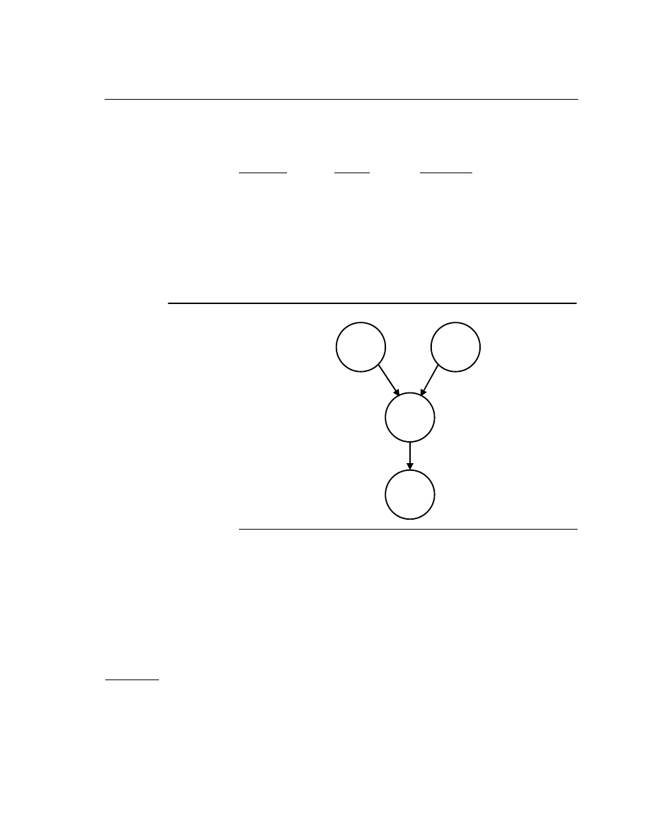
5-26
5
Intel Architecture Optimization Reference Manual
Consider a simple loop that fetches
src1
and
src2
(like in Example 5-12),
multiplies them, and accumulates the multiplication result. The assumptions
are:
Instruction
Latency
Throughput
Load 3
clocks
1
clock
Multiply 4
clocks
2
clocks
Add
1 clock
1 clock
Now examine this simple kernel’s dependency graph in Figure 5-3, and the
schedule, in Table 5-3.
Figure 5-3
Modulo Scheduling Dependency Graph
ld-s1
ld-t1
mul
add

Optimizing Floating-point Applications
5
5-27
Now starting from the schedule for one iteration (above), overlap the
schedule for several iterations in a spreadsheet or in a table as shown in
Table 5-4
.
Table 5-3
EMMS Modulo Scheduling
clk
load
mul
add
0
lds1
1
ldt1
2
ldt2
3
lds2
4
mul1
5
6
mul2
7
8
add1
9
10
add2
Table 5-4
EMMS Schedule – Overlapping Iterations
clk
load
mul
add
0
lds1
prolog
1
ldt1
2
lds2
3
ldt2
4
lds3
mul1
5
ldt3
6
lds4
mul2
7
ldt4
continued

5-28
5
Intel Architecture Optimization Reference Manual
Careful examination of this schedule shows that steady state execution for
this kernel occurs after two iterations. As with any pipelined loop, there is a
prolog and epilog. This is also referred to as loop setup and loop shutdown,
or filling the pipes and flushing the pipes.
Now assume the initiation interval
MRT
(II = 4) and examine the schedule in
How do we schedule this particular scenario and allocate registers? The
Pentium II and Pentium
III
processors can execute instructions out of order.
Example 5-13 shows an improved version of the code, with proper
scheduling resulting in 20% performance increase.
8
lds5
mul3
add1
steady state
9
ldt5
10
lds6
mul4
add2
11
ldt6
12
mul5
add3
epilog
13
14
mul6
add4
15
16
add5
17
18
add6
Table 5-5
Modulo Scheduling with Interval MRT (II=4)
clk
MRT(II=4)
load
mul
add
0
ld
mul
add
1
ld
2
ld
mul
add
3
ld
Table 5-4
EMMS Schedule – Overlapping Iterations (continued)
clk
load
mul
add

Optimizing Floating-point Applications
5
5-29
Example 5-13 Proper Scheduling for Performance Increase
int toy(sptr1, sptr2)
unsigned char *sptr1, *sptr2;
{
asm("pushl %ecx");
asm("movl 12(%ebp), %ebx"); // sptr1
asm("movl 8(%ebp), %eax"); // sptr2
asm("movq (%eax,%ecx), %mm1");
asm("movq (%ebx,%ecx), %mm3");
asm("pxor %mm0, %mm0"); // initialize mm0 to 0
asm("pxor %mm5, %mm5"); // initialize mm5 to 0
asm("pxor %mm6, %mm6"); // initialize mm6 to 0
asm("pxor %mm7, %mm7"); // initialize mm7 to 0
asm("movl 16*stride, %ecx"); // initialize loop
counter
asm("top_of_loop:");
asm("movq 8(%ebx,%ecx), %mm2");
asm("movq 8(%eax,%ecx), %mm4");
asm("paddw %mm5, %mm6");
asm("pmulw %mm3, %mm1")
asm("movq stride(%ebx,%ecx), %mm3");
asm("movq stride(%eax,%ecx), %mm5");
asm("paddw %mm6, %mm7");
asm("pmulw %mm4, %mm2");
asm("movq stride+8(%ebx,%ecx), %mm4");
asm("movq stride+8(%eax,%ecx), %mm6");
asm("paddw %mm7, %mm0");
asm("pmulw %mm5, %mm3");
asm("movq 2*stride(%ebx,%ecx), %mm5");
asm("movq 2*stride(%eax,%ecx), %mm7");
asm("paddw %mm0, %mm1");
asm("pmulw %mm6, %mm4");
asm("movq 2*stride+8(%ebx,%ecx), %mm6");
asm("movq 2*stride+8(%eax,%ecx), %mm0");
_____________________________________________________________
continued

5-30
5
Intel Architecture Optimization Reference Manual
Example 5-13 Proper Scheduling for Performance Increase (continued)
asm("paddw %mm1, %mm2");
asm("pmulw %mm7, %mm5");
asm("movq 3*stride(%ebx,%ecx), %mm7");
asm("movq 3*stride(%eax,%ecx), %mm1");
asm("paddw %mm2, %mm3");
asm("pmulw %mm0, %mm6");
asm("movq 3*stride+8(%ebx,%ecx), %mm0");
asm("movq 3*stride+8(%eax,%ecx), %mm2");
asm("paddw %mm3, %mm4");
asm("pmulw %mm1, %mm7");
asm("movq 4*stride(%ebx,%ecx), %mm1");
asm("movq 4*stride(%eax,%ecx), %mm3");
asm("paddw %mm4, %mm5");
asm("pmulw %mm2, %mm0");
asm("movq 4*stride+8(%ebx,%ecx), %mm2");
asm("movq 4*stride+8(%eax,%ecx), %mm4");
asm("paddw %mm5, %mm6");
asm("pmulw %mm3, %mm1");
asm("subl 4*stride, %ecx");
asm("jg top_of_loop");
// no horizontal reduction needed at the end
asm("movd %mm6, %eax");
asm("popl %ecx");
}
_____________________________________________________________
Example 5-13 also shows that to achieve better performance, it is necessary
to expose the instruction level parallelism to the processor. In exposing the
parallelism keep in mind these considerations:
•
Use the available issue ports.
•
Expose independent instructions such that the processor can schedule
them efficiently.

Optimizing Floating-point Applications
5
5-31
Scheduling to Avoid Register Allocation Stalls
After the µops are decoded, they are allocated into a buffer with the
corresponding data sources to be dispatched to the execution units. If the
sources are already in the dispatch buffer from previous producers of those
sources, then no stalls will happen. However, if producers and consumers
are separated further than needed to resolve dependency, then the producer
results will no longer be in the dispatch buffer when they are needed for the
consuming µops. The general rule of thumb is to try to balance the distance
between the producers and consumers so that dependency will have some
time to resolve, but not so much time that results are not lost from the buffer.
Forwarding from Stores to Loads
Be careful when performing loads from a memory location that was
previously and recently stored, since certain types of store forwarding may
incur a longer latency than others. In particular, storing a result that has a
smaller data size than that of the following load, may result in a longer
latency than if a 64-bit load is used. An example of this is two 64-bit MMX
technology stores (
movq
) followed by a 128-bit Streaming SIMD
Extensions load (
movaps
).
Conditional Moves and Port Balancing
Conditional moves emulation and port balancing can greatly contribute to
your application’s performance gains using the techniques explained in the
following sections.
Conditional Moves
If possible, emulate conditional moves by using masked compares and
logical instructions instead of conditional branches. Mispredicted branches
impede the Pentium
III
processor’s performance. In the Pentium II and
Pentium
III
processors prior to processors with Streaming SIMD
Extensions, execution Port 1 is solely dedicated to 1-cycle latency µops (for
example,
cjmp
). In the Pentium
III
processor, additional execution units
were added to Port 1, to execute new 3-cycle latency µops (
addps
,
subps
,

5-32
5
Intel Architecture Optimization Reference Manual
maxps
...), in addition to the 1-cycle latency µops. Thus, single-cycle µops,
including
cjmp
µop, can be delayed more than in previous Pentium
processors.
Throttling
cjmp
µops delays resolution of mispredicted
cjmp
µops.
Potentially, this can increase the length of the speculation and possibly
execute on an incorrect path. Use
cmov
instead of
cjmp
instruction. In the
Streaming SIMD Extensions, the
cjmp
instruction can be emulated using a
combination of
CMPPS
instruction and logical instructions.
Example 5-14 shows two loops: the first implements conditional branch
instruction, the second omits this instruction.
Example 5-14 Scheduling with Emulated Conditional Branch
//Conditional branch included
loopMax:
cmpnleps xmm1,
xmm0
movmskps
eax, xmm1
cmp eax, 0
je noMax
maxFound:
maxps xmm0,
[esi+ecx]
andps
xmm1,
xmm3
maxps
xmm2,
xmm1
noMax:
add
ecx, 16
addps
xmm3,
xmm4
movaps xmm1,
[esi+ecx]
jnz
loopMax
// Use this structure for better scheduling
loopMax:
cmpnleps xmm5,
xmm0
maxps
xmm0, xmm1
andps
xmm5, xmm3
maxps
xmm2, xmm5
____________________________________________________________
continued

Optimizing Floating-point Applications
5
5-33
Example 5-14 Scheduling with Emulated Conditional Branch (continued)
add
ecx, 16
addps
xmm3, xmm4
movaps
xmm1, [esi+ecx]
movaps
xmm5, xmm1
jnz
loopMax
_____________________________________________________________
The original code’s performance depends on the number of mispredicted
branches which in turn depends on the data being sorted, which contributes
to a large value for clocks per instruction (CPI = 1.78). The second loop
omits the conditional branch instruction, but does not balance the port
loading. A further advantage of the new code is that the latency is
independent of the data values being sorted.
Port Balancing
To further reduce the CPI in the above example, balance the number of µops
issued on ports 0, 1, and 2. You can do so by replacing sections of the
Streaming SIMD Extensions code with MMX technology code. In
particular, calculation of the indices can be done with MMX instructions as
follows:
•
Create a mask with Streaming SIMD Extensions and store into
memory.
•
Convert this mask into MMX technology format using
movq
and
packssdw
instructions.
•
Extract max indices using the MMX technology
pmaxsw
,
pand
, and
paddw
instructions.
The code in Example 5-15 demonstrates these steps.

5-34
5
Intel Architecture Optimization Reference Manual
Example 5-15 Replacing the Streaming SIMD Extensions Code with the MMX
Technology Code
loopMax:
cmpnleps xmm1, xmm0
;create mask in Streaming SIMD
;Extensions format
maxps xmm0, [esi+ecx];get max values
movaps [esi+ecx], xmm1;store mask into memory
movq mm1, [esi+ecx];put lower part of mask into mm1
add
ecx, 16
;increment pointer
movaps xmm1, [esi+ecx];load next four aligned floats
packssdw mm1, [esi+ecx-8];pack lower and upper parts
;of the mask
mask:
pand mm1, mm3 ;get indices mask of max values
paddw mm3, mm4 ;increment indices
pmaxsw mm2, mm1 ;get indices corresponding to max
;values
jnz
loopMax
_____________________________________________________________
Example 5-15 is the most optimal version of code for the Pentium
III
processor and has a CPI of 0.94. This example illustrates the importance of
instruction usage to maximize port utilization. See Appendix C,
“
Instruction to Decoder Specification
,” for a table that details port
assignments of the instructions in the Pentium
III
processor architecture.
Another example where replacing the Streaming SIMD Extensions code
with the MMX technology code can give good results is the dot product
operation. This operation is the primary operation in matrix multiplication
that is used frequently in 3D applications and other floating-point
applications.
The dot product kernel and optimization issues and considerations are
presented in the following discussion. The code in Example 5-16 represents
a typical dot product implementation.

Optimizing Floating-point Applications
5
5-35
Example 5-16 Typical Dot Product Implementation
inner_loop:
movaps (%eax,%ecx,4), %xmm0 // 1st
movaps (%ebx,%ecx,4), %xmm1
mulps %xmm1, %xmm0
addps %xmm0, %xmm7
movaps 16(%eax,%ecx,4), %xmm2 // 2nd
movaps 16(%ebx,%ecx,4), %xmm3
mulps %xmm3, %xmm2
addps %xmm2, %xmm7
movaps 32(%eax,%ecx,4), %xmm4 // 3rd
movaps 32(%ebx,%ecx,4), %xmm5
mulps %xmm5, %xmm4
addps %xmm4, %xmm7
movaps 48(%eax,%ecx,4), %xmm6 // 4th
movaps 48(%ebx,%ecx,4), %xmm0
mulps %xmm6, %xmm0
addps %xmm0, %xmm7
subl $16, %ecx // loop count
jnz inner_loop
_____________________________________________________________
The inner loop in the above example consists of eight loads, four multiplies
and four additions. This translates into 16
load
µops, 8
mul
µops and 8
add
µops for Streaming SIMD Extensions and 8
load
µops, 4
mul
µops and 4
add
µops for MMX technology.
What are the characteristics of the dot product operation?
•
Ratio of
load
/
mult
/
add
µops is 2:1:1.
•
Hardware
load
/
mult
/
add
ports is 1:1:1.
•
Optimum balance of ports for
load
/
mult
/
add
is 1:1:1.
•
Inner loop performance is limited by a single
load
port.
This kernel’s performance can be improved by using optimization
techniques to avoid performance loss due to hardware resource constraints.
Since the optimum latency for the inner loop is 16 clocks, experimenting

5-36
5
Intel Architecture Optimization Reference Manual
with a large number of iterations can reduce branch penalties. Properly
scheduled code achieves 16 clocks/iteration with a large number of
iterations. But, only four iterations are present in the original code. The
increase is caused by a BTB (branch target buffer) warm-up penalty that
occurs in the beginning of the loop. A mispredicted branch occurs on the
last iteration. The warm-up penalty and mispredicted branch combine to
cause about 5 additional clocks/iteration. The cause of the performance loss
is a short loop and a large number of loads.
Streaming SIMD Extension Numeric Exceptions
This section discusses various aspects of the Streaming SIMD Extension
numeric exceptions: conditions, priority, automatic masked exception
handling, software exception handling with unmasked exceptions,
interaction with x87 numeric exceptions, and the flush-to-zero mode.
Exception Conditions
The numeric exception conditions that can occur when executing Streaming
SIMD Extension instructions can be referred to as the following six classes:
•
invalid operation (#I)
•
divide-by-zero (#Z)
•
denormalized operand (#D)
•
numeric overflow (#O)
•
numeric underflow (#U)
•
inexact result (precision) (#P)
Invalid, divide-by-zero and denormal exceptions are precomputation
exceptions; they are detected before any arithmetic operation occurs.
Underflow, overflow and precision exceptions are post-computation
exceptions.
When numeric exceptions occur, a processor supporting Streaming SIMD
Extensions take one of two possible courses of action:
•
The processor can handle the exception by itself, producing the most
reasonable result and allowing numeric program execution to continue
undisturbed (that is, masked exception response).
•
A software exception handler can be invoked to handle the exception
(that is, unmasked exception response).

Optimizing Floating-point Applications
5
5-37
Each of the six exception conditions described above has corresponding flag
and mask bits in the
MXCSR
. Depending on the flag and mask bit values the
following operations take place:
•
If an exception is masked (mask bit in
MXCSR
= 1), the processor takes
an appropriate default action and continues with the computation.
•
If the exception is unmasked (mask bit in
MXCSR
= 0) and the operating
system (OS) supports Streaming SIMD Extension exceptions (that is,
CR4.OSXMMEXCEPT = 1
), a software exception handler is invoked
immediately through Streaming SIMD Extensions exception interrupt
vector 19.
•
If the exception is unmasked (mask bit in
MXCSR
= 0) and the OS does
not support Streaming SIMD Extension exceptions (that is,
CR4.OSXMMEXCEPT = 0
), an invalid opcode exception is signalled
instead of a Streaming SIMD Extensions exception.
Exception Priority
The processor handles exceptions according to a predetermined precedence.
The precedence for Streaming SIMD Extension numeric exceptions is as
follows:
•
Invalid-operation exception
•
QNaN
operand. Though this is not an exception, the handling of a
QNaN
operand has precedence over lower-priority exceptions. For example, a
QNaN
divided by zero results in a
QNaN
, not a zero-divide exception.
•
Any other invalid-operation exception not mentioned above or a
divide-by-zero exception
•
Denormal-operand exception. If masked, then instruction execution
continues, and a lower-priority exception can occur as well
NOTE.
Note that Streaming SIMD Extension exceptions exclude a
situation when, for example, an x87 floating-point instruction,
fwait
, or
a Streaming SIMD Extensions instruction catch a pending unmasked
Streaming SIMD Extensions exception.

5-38
5
Intel Architecture Optimization Reference Manual
•
Numeric overflow and underflow exceptions in conjunction with the
inexact-result exception
•
Inexact-result exception
When a suboperand of a packed instruction generates two or more
exception conditions, the exception precedence sometimes results in the
higher-priority exception being handled and the lower-priority exceptions
being ignored. For example, dividing an
SNaN
by zero can potentially signal
an invalid-arithmetic-operand exception (due to the
SNaN
operand) and a
divide-by-zero exception. Here, if both exceptions are masked, the
processor handles the higher-priority exception only (the invalid-arithmetic-
operand exception), returning a real indefinite to the destination.
Alternately, a denormal-operand or inexact-result exception can accompany
a numeric underflow or overflow exception, with both exceptions being
handled. Prioritizing of exceptions is performed only on a individual
sub-operand basis, and not between suboperands. For example, an invalid
exception generated by one sub-operand will not prevent the reporting of a
divide-by-zero exception generated by another sub-operand.
Automatic Masked Exception Handling
If the processor detects an exception condition for a masked exception, it
delivers a predefined default response and continues executing instructions.
The masked (default) responses to exceptions deliver a reasonable result for
each exception condition and are generally satisfactory for most application
code. By masking or unmasking specific floating-point exceptions in the
MXCSR, programmers can delegate responsibility for most exceptions to
the processor and reserve the most severe exception conditions for software
exception handlers.
Because the exception flags are “sticky,” they provide a cumulative record
of the exceptions that have occurred since they were last cleared. A
programmer can thus mask all exceptions, run a calculation, and then
inspect the exception flags to see if any exceptions were detected during the
calculation.

Optimizing Floating-point Applications
5
5-39
Note that when exceptions are masked, the processor may detect multiple
exceptions in a single instruction, because:
•
Execution continues after performing its masked response; for
example, the processor could detect a denormalized operand, perform
its masked response to this exception, and then detect an underflow.
•
Some exceptions occur naturally in pairs, such as numeric underflow
and inexact result (precision).
•
Packed instructions can produce independent exceptions on each pair
of operands.
Software Exception Handling - Unmasked Exceptions
Most of the masked exceptions in Streaming SIMD Extensions are handled
by hardware without penalty except denormals and underflow. But these can
also be handled without penalty if flush-to-zero mode is used.
Your application must ensure that the operating system supports unmasked
exceptions before unmasking any of the exceptions in the
MXCSR
(see
“Checking for Processor Support of Streaming SIMD Extensions and
MMX™ Technology” in Chapter 3
If the processor detects a condition for an unmasked Streaming SIMD
Extensions application exception, a software handler is invoked
immediately at the end of the excepting instruction. The handler is invoked
through the Streaming SIMD Extensions exception interrupt (vector 19),
irrespective of the state of the
CR0.NE
flag. If an exception is unmasked, but
Streaming SIMD Extension unmasked exceptions are not enabled
(
CR4.OSXMMEXCPT = 0
), an invalid opcode fault is generated. However,
the corresponding exception bit will still be set in the MXCSR, as it would
be if
CR4.OSXMMEXCPT = 1
, since the invalid opcode handler/user needs
to determine the cause of the exception.
A typical action of the exception handler is to store x87 floating-point and
Streaming SIMD Extensions state information in memory (with the
fxsave/fxrstor
instructions) so that it can evaluate the exception and
formulate an appropriate response. Other typical exception handler actions
can include:
•
Examining stored x87 floating-point and Streaming SIMD Extensions
state information (control/status) to determine the nature of the error.

5-40
5
Intel Architecture Optimization Reference Manual
•
Taking action to correct the condition that caused the error.
•
Clearing the exception bits in the x87 floating-point status word (
FSW
)
or the Streaming SIMD Extensions control register (
MXCSR
).
•
Returning to the interrupted program and resuming normal execution.
In lieu of writing recovery procedures, the exception handler can do the
following:
•
Increment in software an exception counter for later display or printing.
•
Print or display diagnostic information (such as the Streaming SIMD
Extensions register state).
•
Halt further program execution.
When an unmasked exception occurs, the processor will not alter the
contents of the source register operands prior to invoking the unmasked
handler. Similarly, the integer
EFLAGS
will also not be modified if an
unmasked exception occurs while executing the
comiss
or
ucomiss
instructions. Exception flags will be updated according to the following
rules:
•
Exception flag updates are generated by a logical-OR of exception
conditions for all sub-operand computations, where the OR is done
independently for each type of exception. For packed computations,
this means four suboperands; for scalar computations this means 1
sub-operand (the lowest one).
•
In the case of only masked exception conditions, all flags will be
updated.
•
In the case of an unmasked precomputation type of exception condition
(that is, denormal input), all flags relating to all precomputation
conditions (masked or unmasked) will be updated, and no subsequent
computation is performed (that is, no post-computation condition can
occur if there is an unmasked pre-computation condition).
•
In the case of an unmasked post-computation exception condition, all
flags relating to all post-computation conditions (masked or unmasked)
will be updated; all precomputation conditions, which must be masked,
will also be reported.

Optimizing Floating-point Applications
5
5-41
Interaction with x87 Numeric Exceptions
The Streaming SIMD Extensions control/status register was separated from
its x87 floating-point counterparts to allow for maximum flexibility.
Consequently, the Streaming SIMD Extensions architecture is independent
of the x87 floating-point architecture, but has the following implications for
x87 floating-point applications that call Streaming SIMD
Extensions-enabled libraries:
•
The x87 floating-point rounding mode specified in
FCW
will not apply
to calls in a Streaming SIMD Extensions library, unless the rounding
control in
MXCSR
is explicitly set to the same mode.
•
x87 floating-point exception observability may not apply to a
Streaming SIMD Extensions library.
•
An application that expects to catch x87 floating-point exceptions that
occur in an x87 floating-point library will not be notified if an
exception occurs in a corresponding Streaming SIMD Extensions
library, unless the exception masks, enabled in
FCW
, have also been
enabled in
MXCSR
.
•
An application will not be able to unmask exceptions after returning
from a Streaming SIMD Extensions library call to detect if an error
occurred. A Streaming SIMD Extensions exception flag that was set
when the corresponding exception was unmasked will not generate a
fault; only the next occurrence of that exception will generate an
unmasked fault.
NOTE.
In certain cases, if any numerical exception is unmasked, the
retirement rate might be affected and reduced. This might happen when
Streaming SIMD Extensions code is scheduled without large impact of
the dependency and with the intention to have maximum execution rate.
Usually such code consists of balanced operations such as packed
floating-point multiply, add and load or store (or a mix that includes
balanced 2 arithmetic operation/load or store with MMX technology or
integer instructions).

5-42
5
Intel Architecture Optimization Reference Manual
•
An application which checks
FSW
to determine if any masked exception
flags were set during an x87 floating-point library call will also need to
check
MXCSR
in order to observe a similar occurrence of a masked
exception within a Streaming SIMD Extensions library.
Use of
CVTTPS2PI
/
CVTTSS2SI
Instructions
The
cvttps2pi
and
cvttss2si
instructions encode the truncate/chop
rounding mode implicitly in the instruction, thereby taking precedence over
the rounding mode specified in the
MXCSR
register. This behavior can
eliminate the need to change the rounding mode from round-nearest, to
truncate/chop, and then back to round-nearest to resume computation.
Frequent changes to the
MXCSR
register should be avoided since there is a
penalty associated with writing this register; typically, through the use of the
cvttps2pi
and
cvttss2si
instructions, the rounding control in
MXCSR
can be always be set to round-nearest.
Flush-to-Zero Mode
Activating the flush-to-zero mode has the following effects during
underflow situations:
•
Zero result is returned when the result is true.
•
Precision and underflow exception flags are set to 1.
The IEEE mandated response to underflow is to deliver the denormalized
result (that is, gradual underflow); consequently, the flush-to-zero mode is
not compatible with IEEE Standard 754. It is provided for applications
where underflow is common. Underflow for flush-to-zero mode occurs
when the exponent for a computed result falls in the denormal range,
regardless of whether a loss of accuracy has occurred.
Unmasking the underflow exception takes precedence over flush-to-zero
mode. For a Streaming SIMD Extensions instruction that generates an
underflow condition an exception handler is invoked. Unmasking the
underflow exception occurs, regardless of whether flush-to-zero mode is
enabled.

6-1
Optimizing
Cache Utilization
for Pentium
®
III
Processors
6
Over the past decade, processor speed has increased more than ten times,
while memory access speed has increased only slightly. Many applications
can considerably improve their performance if data resides in caches so the
processor does not have to wait for the data from memory.
Until now, techniques to bring data into the processor before it was needed
involved additional programming. These techniques were not easy to
implement, or required special steps to prevent from degrading
performance. The Streaming SIMD Extensions address these issues by
providing the prefetch instruction and its variations. Prefetching is a much
better mechanism to ensure that data are in the cache when requested.
The prefetch instruction, controlled by the programs or compilers, retrieves
a minimum of 32 bytes of data prior to the data actually being needed. This
hides the latency for data access in the time required to process data already
resident in the cache. Many algorithms can provide information in advance
about the data that is to be required soon. The new instruction set also
features non-temporal store instructions to minimize the performance issues
caused by cache pollution.
This chapter focuses on two major subjects:
•
Prefetch and Cacheability Instructions—describes instructions that
allow you to implement a data caching strategy.
•
Memory Optimization Using Prefetch—describes and provides
examples of various techniques for implementing prefetch instructions.
Note that in a number of cases presented in this chapter, the prefetching and
cache utilization are platform-specific and may change for future
processors.

6-2
6
Intel Architecture Optimization Reference Manual
Prefetch and Cacheability Instructions
The new cacheability control instructions allow you to control data caching
strategy in order to increase cache efficiency and minimize cache pollution.
Data can be viewed by time and address space characteristics as follows:
Temporal
data will be used again soon
Spatial
data will be used in adjacent locations, for example, the
same cache line
Non-temporal
data which are referenced once and not reused in the
immediate future; for example, some multimedia data
types, such as the vertex buffer in a 3D graphics
application
These data characteristics are used in the discussion that follows.
The Prefetching Concept
The
prefetch
instruction can hide the latency of data accesses in
performance-critical sections of application code by allowing data to be
fetched in advance of its actual usage. The
prefetch
instructions do not
change the user-visible semantics of a program, although they may affect
the program’s performance. The
prefetch
instructions merely provide
hints to the hardware and generally do not generate exceptions or faults.
The
prefetch
(load 32 or greater number of bytes) instructions load either
non-temporal data or temporal data in the specified cache level. This data
access type and the cache level are specified as hints. Depending on the
implementation, the instruction fetches 32 or more aligned bytes, including
the specified address byte, into the instruction-specified cache levels.
NOTE.
Using the
prefetch
instructions is recommended only if data
does not fit in cache.

Optimizing Cache Utilization for Pentium III Processors
6
6-3
Generally the
prefetch
instructions only provide hints to the hardware
and do not generate exceptions or faults except for a special case described
in the
“Prefetch and Load Instructions”
section. However, excessive use of
prefetch instructions may waste memory bandwidth and result in a
performance penalty due to resource constraints.
Nevertheless, the prefetch instructions can lessen the overhead of memory
transactions by preventing cache pollution, and by using the cache and
memory efficiently. This is particularly important for the applications that
share critical system resources, such as memory bus. See an example in
section.
The Prefetch Instructions
The Streaming SIMD Extensions include four types of
prefetch
instructions corresponding to four prefetching hints to the processor: one
non-temporal, and three temporal. They correspond to two types of
operations, temporal and non-temporal.
The non-temporal instruction is
prefetchnta
fetch data into location closest to the processor,
minimizing cache pollution. On the Pentium
®
III
processor, this is the L1 cache.
The temporal instructions are
prefetcht0
fetch data into all cache levels, that is to L1 and L2 for
Pentium
III
processors
prefetcht1
fetch data into all cache levels except the 0
th
level, that is
to L2 only on Pentium
III
processors
prefetcht2
fetch data into all cache levels except the 0
th
and 1
st
levels, that is, to L2 only on Pentium
III
processors
NOTE.
If the data are already found in a cache level that is closer to the
processor at the time of
prefetch
, no data movement occurs.

6-4
6
Intel Architecture Optimization Reference Manual
In the description above, cache level 0 is closest to the processor. For
Streaming SIMD Extensions implementation, there are only two cache
levels, L1 and L2. L1 is the 0
th
cache level by the architectural definition, as
a result,
prefetcht1
and
prefetcht2
are designed to behave the same in
Pentium
®
III
processor. For future processors, this may change.
Prefetchnta
with Streaming SIMD Extensions implementation fetches
data into L1 only, therefore minimizing L2 cache pollution.
Prefetch
instructions are mainly designed to improve application
performance by hiding memory latency in the background. If segments of
an application access data in a predictable manner, for example, using
arrays with known strides, then they are good candidates for using prefetch
to improve performance. However, if a program is memory throughput
bound, that is, memory access time is much larger than execution time, then
there may be not much benefit from utilizing prefetch.
Basically, use
prefetch
in:
•
predictable memory access patterns
•
time-consuming innermost loops
•
locations where execution pipeline stalls for data from memory due to
flow dependency
Prefetch and Load Instructions
The Pentium II and Pentium
III
processors have a decoupled execution and
memory architecture that allows instructions to be executed independently
with memory accesses if there is no data and resource dependency.
Programs or compilers can use dummy load instructions to imitate prefetch
functionality, but preloading is not equivalent to prefetching. Prefetch
instructions provide a greater performance than preloading.
Currently, the
prefetch
instruction provides a greater performance gain
than preloading because it:
•
has no register destination, it only updates cache lines;
•
does not stall the normal instruction retirement;
•
does not affect the functional behavior of the program;
•
has no cache line split accesses;

Optimizing Cache Utilization for Pentium III Processors
6
6-5
•
does not cause exceptions except when the
LOCK
prefix is used; for
Pentium
III
processors, an invalid opcode exception is generated when
the
LOCK
prefix is used with prefetch instructions;
•
does not complete its own execution if that would cause a fault;
•
is ignored if the
prefetch
targets an uncacheable memory region, for
example, USWC and UC;
•
does not perform a page table walk if it results in a page miss.
The current advantages of the prefetch over preloading instructions are
processor-specific. The nature and extent of the advantages may change in
the future.
The Non-temporal Store Instructions
The non-temporal store instructions (
movntps
,
movntq
, and
maskmovq
)
minimize cache pollution while writing data. The main difference between a
non-temporal store and a regular cacheable store is in the write-allocation
behavior: the processor will fetch the corresponding cache line into the
cache hierarchy prior to performing the store and the memory type can take
precedence over the non-temporal hint.
Currently, if you specify a non-temporal store to cacheable memory, they
must maintain coherency. Two cases may occur:
•
If the data are present in the cache hierarchy, the data are updated in-
place and the existing memory type attributes are retained. For
example, in Streaming SIMD Extensions implementation, if there is a
data hit in L1, then non-temporal stores behave like regular stores.
Otherwise, write to memory without cache line allocation. If the data
are found in L2, data in L2 will be invalidated.
•
If the data are not present in the cache hierarchy, the memory type
visible on the bus will remain unchanged, and the transaction will be
weakly-ordered; consequently, you are responsible for maintaining
coherency. Non-temporal stores will not write allocate. Different
implementations may choose to collapse and combine these stores
inside the processor.
The behavior described above is platform-specific and may change in the
future.

6-6
6
Intel Architecture Optimization Reference Manual
The
sfence
Instruction
The
sfence
(
store fence
) instruction makes it possible for every
store
instruction that precedes the
sfence
instruction in program order to be
globally visible before any
store
instruction that follows the
fence
. The
sfence
instruction provides an efficient way of ensuring ordering between
routines that produce weakly-ordered results.
The use of weakly-ordered memory types can be important under certain
data sharing relationships, such as a producer-consumer relationship. Using
weakly-ordered memory can make assembling the data more efficient, but
care must be taken to ensure that the consumer obtains the data that the
producer intended to see. Some common usage models may be affected in
this way by weakly-ordered stores. Examples are:
•
library functions, which use weakly-ordered memory to write results
•
compiler-generated code, which also benefits from writing
weakly-ordered results
•
hand-crafted code
The degree to which a consumer of data knows that the data is
weakly-ordered can vary for these cases. As a result, the
sfence
instruction
should be used to ensure ordering between routines that produce
weakly-ordered data and routines that consume this data. The
sfence
instruction provides a performance-efficient way by ensuring the ordering
when every
store
instruction that precedes the
store fence
instruction
in program order is globally visible before any
store
instruction which
follows the
fence
.
Streaming Non-temporal Stores
In Streaming SIMD Extensions, the
movntq
,
movnts
and
maskmovq
instructions are streaming, non-temporal stores. With regard to memory
characteristics and ordering, they are similar mostly to the
Write-Combining (
WC
) memory type:
•
Write combining – successive writes to the same cache line are
combined
•
Write collapsing – successive writes to the same byte(s) result in only
the last write being visible

Optimizing Cache Utilization for Pentium III Processors
6
6-7
•
Weakly ordered – no ordering is preserved between
WC
stores, or
between
WC
stores and other loads or stores
•
Uncacheable and not write-allocating – stored data is written around
the cache and will not generate a read-for-ownership bus request for the
corresponding cache line.
Because streaming stores are weakly ordered, a fencing operation is
required to ensure that the stored data is flushed from the processor to
memory. Failure to use an appropriate fence may result in data being
“trapped” within the processor and will prevent visibility of this data by
other processors or system agents. WC stores require software to ensure
coherence of data by performing the fencing operation.
Streaming SIMD Extensions introduce the
sfence
instruction, which now
is solely used to flush
WC
data from the processor. The
sfence
instruction
replaces all other store fencing instructions such as
xchg
.
Streaming stores can improve performance in the following ways:
•
Increase store bandwidth since they do not require read-for-ownership
bus requests
•
Reduce disturbance of frequently used cached (temporal) data, since
they write around the processor caches
Streaming stores allow cross-aliasing of memory types for a given memory
region; for instance, a region may be mapped as write-back (
WB
) via the
page tables (
PAT
) or memory type range registers (
MTRR
s) and yet is written
using a streaming store.
If a streaming store finds the corresponding line already present in the
processor’s caches, several actions may be taken depending on the specific
processor implementation:
Approach A
The streaming store may be combined with the existing
cached data, and is thus treated as a
WB
store (that is, it is
not written to system memory).
Approach B
The corresponding line may be flushed from the
processor’s caches, along with data from the streaming
store.

6-8
6
Intel Architecture Optimization Reference Manual
Pentium
III
processor implements a combination of both approaches. If the
streaming store hits a line that is present in the L1 cache, the store data will
be combined in place within the L1. If the streaming store hits a line present
in the L2, the line and stored data will be flushed from the L2 to system
memory. Note that the approaches, separate or combined, can be different
for future processors.
The two primary usage domains for streaming store are coherent requests
and non-coherent requests.
Coherent Requests
Coherent requests are normal loads and stores to system memory, which
may also hit cache lines present in another processor in a multi-processor
environment. With coherent requests, a streaming store can be used in the
same way as a regular store that has been mapped with a
WC
memory type
(
PAT
or
MTRR
). An
sfence
instruction must be used within a
producer-consumer usage model, in order to ensure coherency and visibility
of data between processors. Within a single-processor system, the CPU can
also re-read the same memory location and be assured of coherence (that is,
a single, consistent view of this memory location): the same is true for a
multi-processor (MP) system, assuming an accepted MP software
producer-consumer synchronization policy is employed.
Non-coherent Requests
Non-coherent requests arise from an I/O device, such as an AGP graphics
card, that reads or writes system memory using non-coherent requests,
which are not reflected on the processor bus and thus will not query the
processor’s caches. An
sfence
instruction must be used within a
producer-consumer usage model, in order to ensure coherency and visibility
of data between processors. In this case, if the processor is writing data to

Optimizing Cache Utilization for Pentium III Processors
6
6-9
the I/O device, a streaming store can be used with a processor with any
behavior of approach A,
above, only if the region has also been mapped
with a
WC
memory type (
PAT, MTRR
).
In case the region is not mapped as
WC
, the streaming might update in-place
in the cache and a subsequent
sfence
would not result in the data being
written to system memory. Explicitly mapping the region as
WC
in this case
ensures that any data read from this region will not be placed in the
processor’s caches. A read of this memory location by a non-coherent I/O
device would return incorrect/out-of-date results. For a processor which
solely implements approach B, above, a streaming store can be used in this
non-coherent domain without requiring the memory region to also be
mapped as
WB
, since any cached data will be flushed to memory by the
streaming store.
Other Cacheability Control Instructions
The
maskmovq
(non-temporal byte mask store of packed integer in an
MMX™ technology register) instruction stores data from an MMX
technology register to the location specified by the
edi
register. The most
significant bit in each byte of the second MMX technology mask register is
used to selectively write the data of the first register on a per-byte basis. The
instruction is implicitly weakly-ordered (that is, successive stores may not
write memory in original program-order), does not write-allocate, and thus
minimizes cache pollution.
The
movntq
(non-temporal store of packed integer in an MMX technology
register) instruction stores data from an MMX technology register to
memory. The instruction is implicitly weakly-ordered, does no
write-allocate, and so minimizes cache pollution.
CAUTION.
Failure to map the region as
WC
may allow the line to be
speculatively read into the processor caches, that is, via the wrong path
of a mispredicted branch.

6-10
6
Intel Architecture Optimization Reference Manual
The
movntps
(non-temporal store of packed single precision floating point)
instruction is similar to
movntq
. It stores data from a Streaming SIMD
Extensions register to memory in 16 byte granularity. Unlike
movntq
, the
memory address must be aligned to a 16-byte boundary; or a general
protection exception will occur. The instruction is implicitly
weakly-ordered, does not write-allocate, and thus minimizes cache
pollution.
Memory Optimization Using Prefetch
Achieving the highest level of memory optimization using prefetch
instructions requires an understanding of the micro-architecture and system
architecture of a given machine. This section translates the key architectural
implications into several simple guidelines for programmers to use.
Figure 6-1 and Figure 6-2 show two scenarios of a simplified 3D geometry
pipeline as an example. A 3D-geometry pipeline typically fetches one
vertex record at a time and then performs transformation and lighting
functions on it. Both figures show two separate pipelines, an execution
pipeline, and a memory pipeline (front-side bus). Since the Pentium II and
Pentium
III
processors completely decouple the functionality of execution
and memory access, these two pipelines can function concurrently. Figure
6-1 shows “bubbles” in both the execution and memory pipelines. When
loads are issued for accessing vertex data, the execution units sit idle and
wait until data is returned. On the other hand, the memory bus sits idle while
the execution units are processing vertices. This scenario severely decreases
the advantage of having a decoupled architecture.
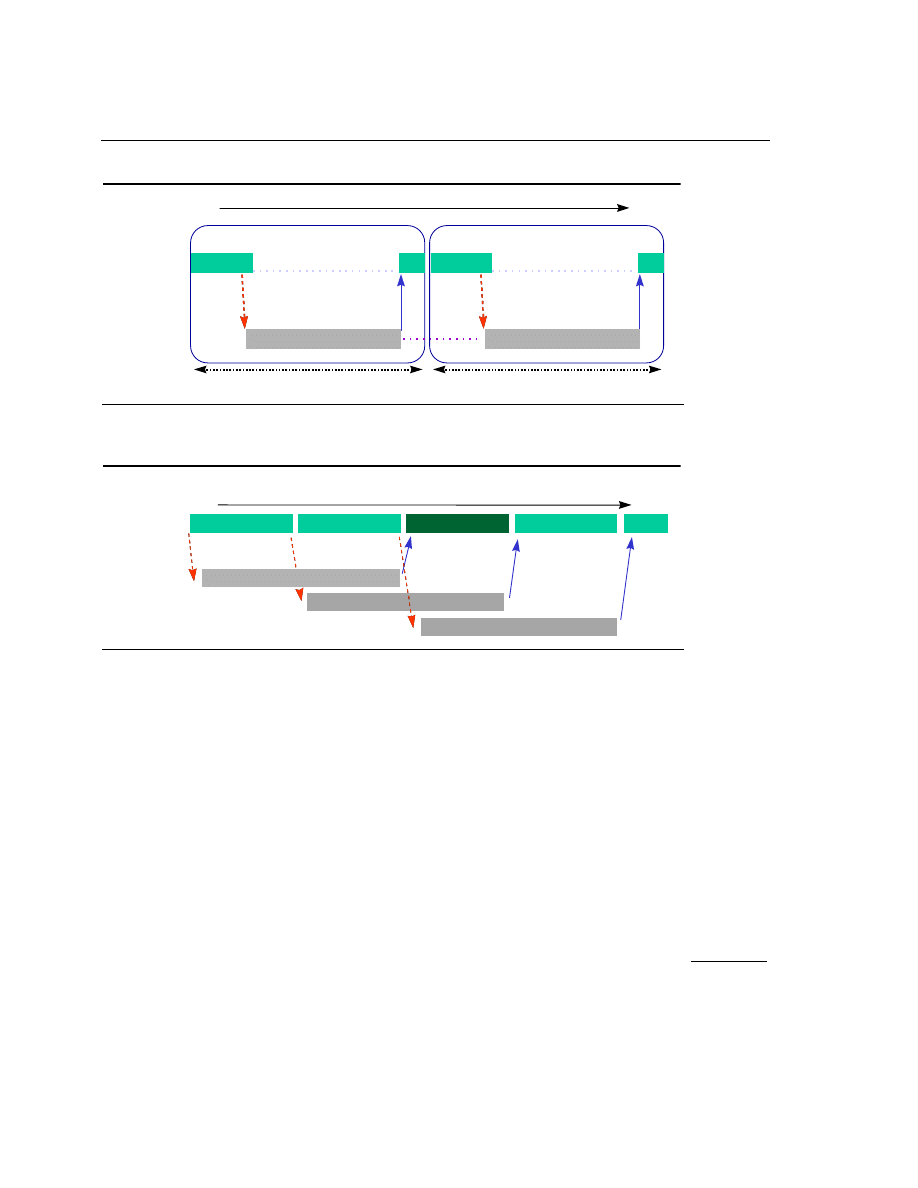
Optimizing Cache Utilization for Pentium III Processors
6
6-11
Figure 6-1
Memory Access Latency and Execution Without Prefetch
Figure 6-2
Memory Access Latency and Execution With Prefetch
The performance loss caused by poor utilization of the resource can be
completely eliminated by applying prefetch instructions appropriately. As
shown in Figure 6-2, prefetch instructions are issued two vertex iterations
ahead. This assumes that only one vertex gets processed in one iteration and
a new data cache line is needed for each iteration. As a result, when iteration
n, vertex V
n
, is being processed, the requested data is already brought into
cache. In the meantime, the front-side bus is transferring the data needed for
n+1 iteration, vertex V
n+1
. Because there is no dependency between V
n+1
data and the execution of V
n
, the latency for data access of V
n+1
can be
entirely hidden behind the execution of V
n
. Under such circumstances, no
“bubbles” are present in the pipelines and thus the best possible
performance can be achieved.
Time
Execution
pipeline
Mem latency
Front-Side
Bus
Vertex n
Issue loads
(vertex data)
Execution units idle
FSB idle
Mem latency
Issue loads
Execution units idle
Vertex n+1
prefetch
Execution
pipeline
Front-Side
Bus
Vertex n-2
issue prefetch
for vertex n
Vertex n-1
Vertex n
Vertex n
Vertex n+1
Time
prefetch
V
n+1
Mem latency for V
n
Mem latency for V
n+1
Mem latency for V
n+2
v
n+2

6-12
6
Intel Architecture Optimization Reference Manual
The software-controlled prefetch instructions provided in Streaming SIMD
Extensions not only hide the latency of memory accesses if properly
scheduled, but also allow you to specify where in the cache hierarchy the
data should be placed. Prefetching is useful for inner loops that have heavy
computations, or are close to the boundary between being compute-bound
and memory-bandwidth-bound. The prefetch is probably not very useful for
loops which are predominately memory bandwidth-bound. When data are
already located in the 0
th
level cache, prefetching can be useless and could
even slow down the performance because the extra µops either back up
waiting for outstanding memory accesses or may be dropped altogether.
This behavior is platform-specific and may change in the future.
Prefetching Usage Checklist
To use the prefetch instruction properly, check whether the following issues
are addressed and/or resolved:
•
prefetch scheduling distance
•
prefetch concatenation
•
minimize the number of prefetches
•
mixing prefetch with computation instructions
•
cache blocking techniques (for example, strip mining)
•
single-pass versus multi-pass execution
•
memory bank conflict issues
•
cache management issues
The subsequent sections discuss all the above items.
Prefetch Scheduling Distance
Determining the ideal prefetch placement in the code depends on many
architectural parameters, including the amount of memory to be prefetched,
cache lookup latency, system memory latency, and estimate of computation
cycle. The ideal distance for prefetching data is processor- and platform-
dependent. If the distance is too short, the prefetch will not effectively hide
the latency of the fetch behind computation. If the prefetch is too far ahead,
the start-up cost for data not prefetched for initial iterations diminishes the
benefits of prefetching the data. Also, the prefetched data may wrap around
and dislodge previously prefetched data prior to its actual use.

Optimizing Cache Utilization for Pentium III Processors
6
6-13
Since prefetch distance is not a well-defined metric, for this discussion, we
define a new term, “prefetch scheduling distance (PSD),” which is
represented in the number of iterations. For large loops, prefetch scheduling
distance can be set to 1, that is, schedule prefetch instructions one iteration
ahead. For small loops, that is, loop iterations with little computation, the
prefetch scheduling distance must be more than one.
A simplified equation to compute PSD is deduced from the mathematical
model. For a simplified equation, complete mathematical model, and
detailed methodology of prefetch distance determination, refer to
Appendix F, “
The Mathematics of Prefetch Scheduling Distance
In Example 6-1, the prefetch scheduling distance is set to 3.
Example 6-1 Prefetch Scheduling Distance
top_loop:
prefetchnta [edx + esi + 32*3]
prefetchnta [edx*4 + esi + 32*3]
. . . . .
movaps
xmm1, [edx + esi]
movaps
xmm2, [edx*4 + esi]
movaps
xmm3, [edx + esi + 16]
movaps
xmm4, [edx*4 + esi + 16]
. . . . .
. . . . .
add
esi, 32
cmp
esi, ecx
jl top_loop
____________________________________________________________
Prefetch Concatenation
De-pipelining memory generates bubbles in the execution pipeline. To
explain this performance issue, a 3D geometry pipeline processing 3D
vertices in strip format is used. A strip contains a list of vertices whose
predefined vertex order forms contiguous triangles.

6-14
6
Intel Architecture Optimization Reference Manual
It can be easily observed that the memory pipe is de-pipelined on the strip
boundary due to ineffective prefetch arrangement. The execution pipeline is
stalled for the beginning 2 iterations for each strip. As a result, the average
latency for completing an iteration will be 165 clocks. (See Appendix F,
“
The Mathematics of Prefetch Scheduling Distance
,” for detailed memory
pipeline description.)
This memory de-pipelining creates inefficiency in both the memory pipeline
and execution pipeline. This de-pipelining effect can be removed by
applying a technique called prefetch concatenation. With this technique, the
memory access and execution can be fully pipelined and fully utilized.
For nested loops, memory de-pipelining could occur during the interval
between the last iteration of an inner loop and the next iteration of its
associated outer loop. Without paying special attention to prefetch insertion,
the loads from the first iteration of an inner loop can miss the cache and stall
the execution pipeline waiting for data returned, thus degrading the
performance.
In the code of Example 6-2, the cache line containing
a[ii][0]
is not
prefetched at all and always misses the cache. This assumes that no array
a[][]
footprint resides in the cache. The penalty of memory de-pipelining
stalls can be amortized across the inner loop iterations. However, it may
become very harmful when the inner loop is short. In addition, the last
prefetch of the inner loop is wasted and consumes machine resources.
Prefetch concatenation is introduced here in order to eliminate the
performance issue of memory de-pipelining.
Example 6-2 Using Prefetch Concatenation
for (ii = 0; ii < 100; ii++) {
for (jj = 0; jj < 32; jj+=8) {
prefetch a[ii][jj+8]
computation a[ii][jj]
}
}
_____________________________________________________________

Optimizing Cache Utilization for Pentium III Processors
6
6-15
Prefetch concatenation can bridge the execution pipeline bubbles between
the boundary of an inner loop and its associated outer loop. Simply by
unrolling the last iteration out of the inner loop and specifying the effective
prefetch address for data used in the following iteration, the performance
loss of memory de-pipelining can be completely removed. The re-written
code is demonstrated in Example 6-3.
Example 6-3 Concatenation and Unrolling the Last Iteration of Inner Loop
for (ii = 0; ii < 100; ii++) {
for (jj = 0; jj < 24; jj+=8) {
prefetch a[ii][jj+8]
computation a[ii][jj]
}
prefetch a[ii+1][0]
computation a[ii][jj]
}
_____________________________________________________________
This code segment for data prefetching is improved, and only the first
iteration of the outer loop suffers any memory access latency penalty,
assuming the computation time is larger than the memory latency. Inserting
a prefetch of the first data element needed prior to entering the nested loop
computation would eliminate or reduce the start-up penalty for the very first
iteration of the outer loop. This uncomplicated high-level code optimization
can improve memory performance significantly.
Minimize Number of Prefetches
Prefetch instructions are not completely free in terms of bus cycles, machine
cycles and resources, even though they require minimal clocks and memory
bandwidth.
Excessive prefetching may lead to the following situations:
•
If the fill buffer is full, prefetches accumulate inside the load buffer
waiting for the next fill buffer entry to be deallocated.
•
If the load buffer is full, instruction allocation stalls.
•
If the target loops are small, excessive prefetching may impose extra
overhead.

6-16
6
Intel Architecture Optimization Reference Manual
A fill buffer is a temporary space allocated for cache line read from or write
to memory. A load buffer is a scratch pad buffer used by the memory
subsystem to impose access ordering on memory loads.
One approach to solve the excessive prefetching issue is to unroll and/or
software-pipeline the loops to reduce the number of prefetches required.
Example 6-4 shows a code example that implements prefetch and unrolls
the loop to remove the redundant prefetch instructions whose prefetch
addresses hit the previously issued prefetch instructions. In this particular
example, unrolling the original loop once saves two prefetch instructions
and three instructions for each conditional jump in every other iteration.
Example 6-4 Prefetch and Loop Unrolling
_________________________________________________________________________
Mix Prefetch with Computation Instructions
It may seem convenient to insert all the prefetch instructions at the
beginning of a loop, but this can lead to severe performance degradation. In
order to achieve best possible performance, prefetch instructions must be
interspersed with other computational instructions in the instruction
top_loop:
prefetchnta [edx+esi+32]
prefetchnta [edx*4+esi+32]
. . . . .
movaps xmm1, [edx+esi]
movaps xmm2, [edx*4+esi]
. . . . .
add esi, 16
cmp esi, ecx
jl top_loop
top_loop:
prefetchnta [edx+esi+32]
prefetchnta [edx*4+esi+32]
. . . . .
movaps xmm1, [edx+esi]
movaps xmm2, [edx*4+esi]
. . . . .
. . . . .
movaps xmm1, [edx+esi+16]
movaps xmm2, [edx*4+esi+16]
. . . . .
add esi, 32
cmp esi, ecx
jl top_loop
un
ro
lled
it
erat
ion
Optimizing Cache Utilization for Pentium III Processors
6
6-17
sequence rather than clustered together. This improves the instruction level
parallelism and reduces the potential instruction allocation stalls due to the
load-buffer-full problem mentioned earlier. It also allows potential dirty
writebacks (additional bus traffic caused by evicting modified cache lines
from the cache) to proceed concurrently with other instructions.
Example 6-5 illustrates mixing prefetch instructions. A simple and useful
heuristic of prefetch spreading for a 500 MHz Pentium
III
processor is to
insert a prefetch instruction every 20 to 25 cycles. Rearranging prefetch
instructions could yield a noticeable speedup for the code which is limited
in cache resource.
Example 6-5 Spread Prefetch Instructions
top _loop:
prefetchnta [ebx+128]
prefetchnta [ebx+1128]
prefetchnta [ebx+2128]
prefetchnta [ebx+3128]
. . . .
. . . .
prefetchnta [ebx+17128]
prefetchnta [ebx+18128]
prefetchnta [ebx+19128]
prefetchnta [ebx+20128]
. . . .
. . . .
mulps xmm3, [ebx+4000]
addps xmm1, [ebx+1000]
addps xmm2, [ebx+3016]
mulps xmm1, [ebx+2000]
mulps xmm1, xmm2
. . . . . . . .
. . . . . .
. . . . .
add ebx, 32
cmp ebx, ecx
jl top_loop
top _loop:
prefetchnta [ebx+128]
movps xmm1, [
ebx]
addps xmm2, [ebx+3000]
mulps xmm3, [ebx+4000]
prefetchnta [ebx+1128]
addps xmm1, [ebx+1000]
addps xmm2, [ebx+3016]
prefetchnta [ebx+2128]
mulps xmm1, [ebx+2000]
mulps xmm1, xmm2
prefetchnta [ebx+3128]
. . . . . . .
. . .
prefetchnta [ebx+18128]
. . . . . .
prefetchnta [ebx+19128]
. . . . . .
. . . .
prefetchnta [ebx+20128]
add ebx, 32
cmp ebx, ecx
jl top_loop
spread prefetches

6-18
6
Intel Architecture Optimization Reference Manual
If all fill buffer entries are full, the next transaction waits inside the load
buffer or store buffer. A prefetch operation cannot complete until a fill
buffer entry is allocated. The load buffers are shared by normal load µops
and outstanding prefetches.
Prefetch and Cache Blocking Techniques
Cache blocking techniques, such as strip-mining, are used to improve
temporal locality, and thereby, cache hit rate. Strip-mining is a
one-dimensional temporal locality optimization for memory. When
two-dimensional arrays are used in programs, loop blocking techniques
(similar to strip-mining but in two dimensions) can be applied for better
memory performance.
If an application uses a large data set that can be reused across multiple
passes of a loop, it will benefit from strip mining: data sets larger than the
cache will be processed in groups small enough to fit into cache. This
allows temporal data to reside in the cache longer, reducing bus traffic.
Data set size and temporal locality (data characteristics) fundamentally
affect how prefetch instructions are applied to strip-mined code. shows two
simplified scenarios for temporally adjacent data and temporally
non-adjacent data.
NOTE.
To avoid instruction allocation stalls due to a load buffer full
condition when mixing prefetch instructions, prefetch instructions must
be interspersed with computational instructions.
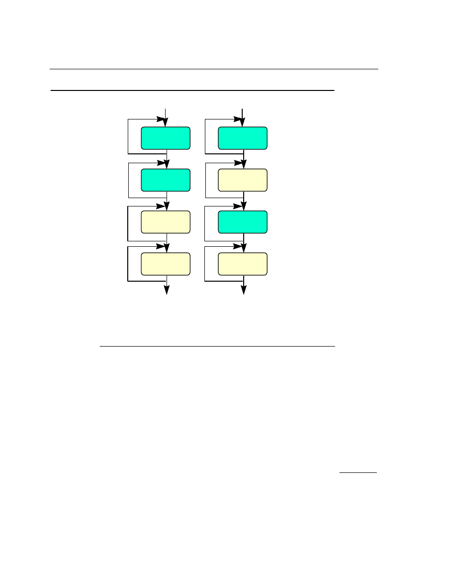
Optimizing Cache Utilization for Pentium III Processors
6
6-19
In the temporally adjacent scenario, subsequent passes use the same data
and find it ready in L1 cache. Prefetch issues aside, this is the preferred
situation. In the temporally non-adjacent scenario, data used in pass m is
displayed by pass (m+1), requiring data re-fetch if a later pass reuses the
data. Both data sets could still fit into L2 cache, so load operations in passes
3 and 4 become less expensive.
Figure 6-4 shows how prefetch instructions and strip-mining can be applied
to increase performance in both of these scenarios.
Figure 6-3
Cache Blocking - Temporally Adjacent and Non-adjacent Passes
Dataset A
Dataset B
Dataset B
Dataset A
Dataset A
Dataset A
Dataset B
Dataset B
Pass 1
Pass 2
Pass 3
Pass 4
Temporally
adjacent passes
Temporally
non-adjacent
passes
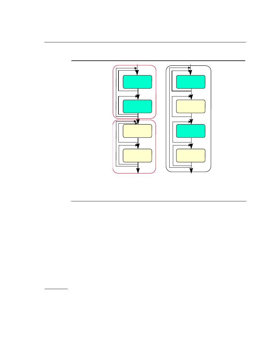
6-20
6
Intel Architecture Optimization Reference Manual
Figure 6-4
Examples of Prefetch and Strip-mining for Temporally Adjacent and
Non-adjacent Passes Loops
For Pentium
III
processors, the left scenario shows a graphical
implementation of using
prefetchnta
to prefetch data into the L1 cache
only (SM1 - strip mine L1), minimizing L2 cache pollution. Use
prefetchnta
if the data set fits into L1 cache or if the data is only touched
once during the entire execution pass in order to minimize cache pollution
in the higher level caches. This provides instant availability when the read
access is issued and minimizes L2 cache pollution.
In the right scenario, keeping the data in L1 cache does not improve cache
locality. Therefore, use
prefetcht0
to prefetch the data. This hides the
latency of the memory references in passes 1 and 2, and keeps a copy of the
Temporally
non-adjacent
passes
Temporally
adjacent passes
Prefetchnta
Dataset
Α
Reuse
Dataset A
Reuse
Dataset B
Prefetchnta
Dataset B
SM1
SM1
Prefetcht0
Dataset A
Prefetcht0
Dataset B
Reuse
Dataset B
Reuse
Dataset A
SM2

Optimizing Cache Utilization for Pentium III Processors
6
6-21
data in L2 cache, which reduces memory traffic and latencies for passes 3
and 4. To further reduce the latency, it might be worth considering extra
prefetchnta
instructions prior to the memory references in passes 3
and 4.
In Example 6-6, consider the data access patterns of a 3D geometry engine
first without strip-mining and then incorporating strip-mining. Note that
4-wide SIMD instructions of Pentium
III
processors can process 4 vertices
per every iteration.
Example 6-6 Data Access of a 3D Geometry Engine without Strip-mining
while (nvtx < MAX_NUM_VTX) {
prefetchnta vertex
i
data // v =[x,y,z,nx,ny,nz,tu,tv]
prefetchnta vertex
i+1
data
prefetchnta vertex
i+2
data
prefetchnta vertex
i+3
data
TRANSFORMATION code // use only x,y,z,tu,tv of a
vertex
nvtx+=4
}
while (nvtx < MAX_NUM_VTX) {
prefetchnta vertex
i
data // v =[x,y,z,nx,ny,nz,tu,tv]
prefetchnta vertex
i+1
data
prefetchnta vertex
i+2
data
prefetchnta vertex
i+3
data
compute the light vectors // use only x,y,z
POINT LIGHTING code // use only nx,ny,nz
nvtx+=4
_____________________________________________________________
Without strip-mining, all four vertices of the lighting loop must be
re-fetched from memory in the second pass. This causes under-utilization of
cache lines fetched during the transformation loop as well as extra
bandwidth wasted in the lighting loop. Now consider the code in Example
6-7 where strip-mining has been incorporated into the loops.

6-22
6
Intel Architecture Optimization Reference Manual
Example 6-7 Data Access of a 3D Geometry Engine with Strip-mining
while (nstrip < NUM_STRIP) {
/* Strip-mine the loop to fit data into L1 */
while (nvtx < MAX_NUM_VTX_PER_STRIP) {
prefetchnta vertex
i
data // v=[x,y,z,nx,ny,nz,tu,tv]
prefetchnta vertex
i+1
data
prefetchnta vertex
i+2
data
prefetchnta vertex
i+3
data
TRANSFORMATION code
nvtx+=4
}
while (nvtx < MAX_NUM_VTX_PER_STRIP) {
/* x y z coordinates are in L1, no prefetch is
required */
compute the light vectors
POINT LIGHTING code
nvtx+=4
}
}
_____________________________________________________________
With strip-mining, all the vertex data can be kept in the cache (for example,
L1) during the strip-mined transformation loop and reused in the lighting
loop. Keeping data in the cache reduces both bus traffic and the number of
prefetches used.
Figure 6-5 summarizes the steps of the basic usage model incorporating
prefetch with strip-mining which are:
•
Do strip-mining: partition loops so that the data set fits into L1 cache
(preferred) or L2 cache.
•
Use
prefetchnta
if the data is only used once or the data set fits into
L1 cache. Use
prefetcht0
if the data set fits into L2 cache.
The above steps are platform-specific and provide an implementation
example.
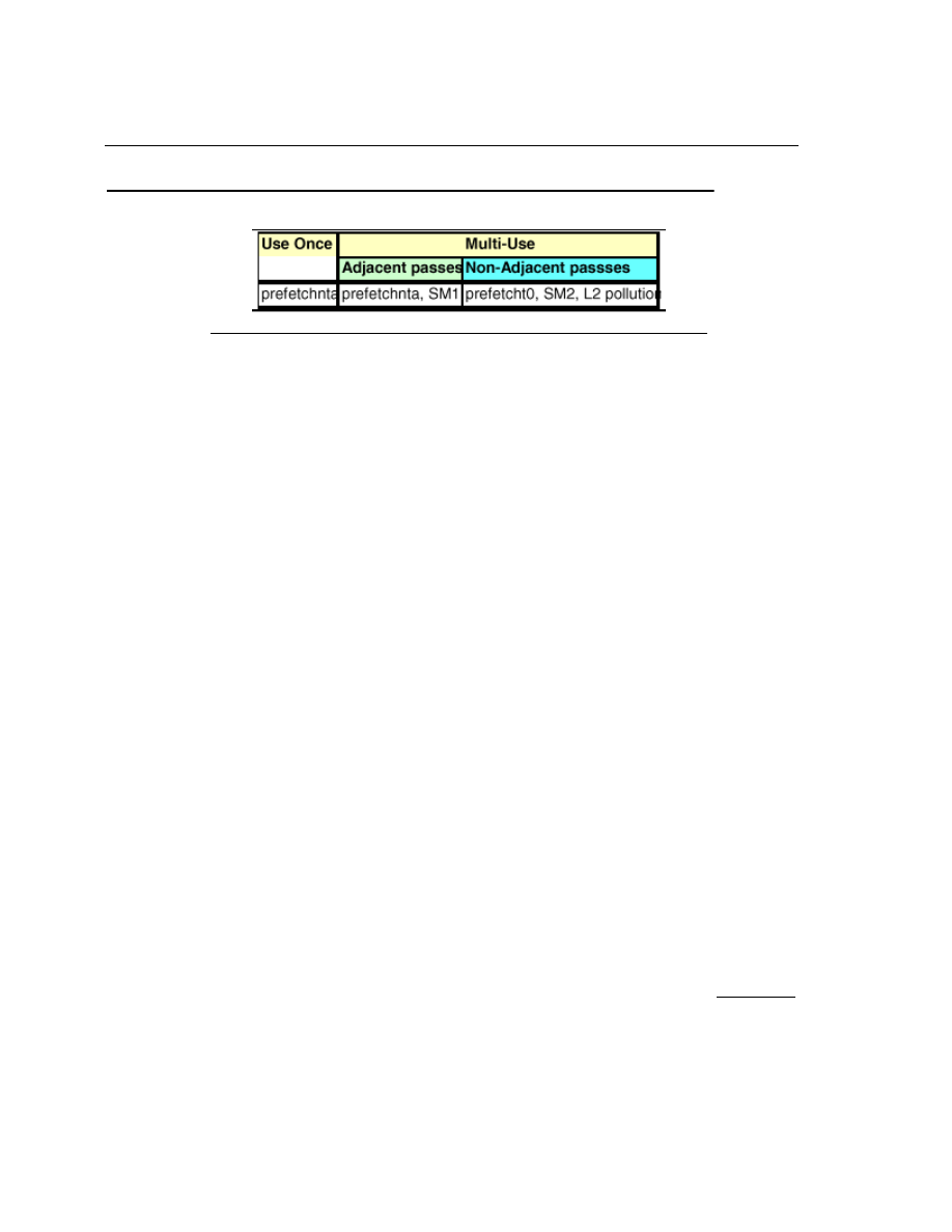
Optimizing Cache Utilization for Pentium III Processors
6
6-23
Single-pass versus Multi-pass Execution
An algorithm can use single- or multi-pass execution defined as follows:
•
Single-pass, or unlayered execution passes a single data element through
an entire computation pipeline.
•
Multi-pass, or layered execution performs a single stage of the pipeline
on a batch of data elements, before passing the batch on to the next
stage.
A characteristic of both single-pass and multi-pass execution is that a specific
tradeoff exists depending on an algorithm’s implementation and use of a
single- or multiple-pass execution, see Figure 6-6.
Multi-pass execution is often easier to use when implementing a general
purpose API, which has lots of different code paths that can be taken,
depending on the specific combination of features selected by the application
(for example, for 3D graphics, this might include the type of vertex
primitives used, the number and type of light sources).
With such a broad range of permutations possible, a single-pass approach
would be complicated, in terms of code size and validation. In such cases,
each possible permutation would require a separate code sequence. For
example, data object of type N, with features A, C, E enabled, would be one
code path. It makes more sense to perform each pipeline stage as a separate
pass, with conditional clauses to select different features that are
implemented within each stage. By using strip-mining, the amount of
vertices processed by each stage (for example, the batch size) can be selected
to ensure that the batch stays within the processor caches through all passes.
An intermediate cached buffer is used to pass the batch of vertices from one
stage/pass to the next one.
Figure 6-5
Benefits of Incorporating Prefetch into Code
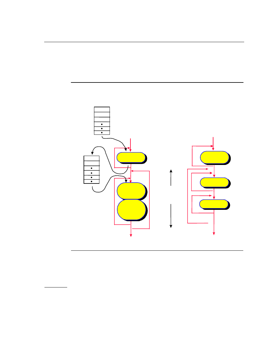
6-24
6
Intel Architecture Optimization Reference Manual
Single-pass execution can be better suited to some applications, which limit
the number of features that may be used at a given time. A single-pass
approach can reduce the amount of data copying that can occur with a
multi-pass engine, see Figure 6-6.
Figure 6-6
Single-Pass vs. Multi-Pass 3D Geometry Engines
Transform
Lighting
Single-Pass
Culling
Lighting
Multi-Pass
Culling
40 vis
40 vis
60 invis
80 vis
80 vis
Vertex
processing
(inner loop)
Outer loop is
processing
strips
Transform
strip list

Optimizing Cache Utilization for Pentium III Processors
6
6-25
The choice of single-pass or multi-pass can have a number of performance
implications. For instance, in a multi-pass pipeline, stages that are limited
by bandwidth (either input or output) will reflect more of this performance
limitation in overall execution time. In contrast, for a single-pass approach,
bandwidth-limitations can be distributed/amortized across other
computation-intensive stages. Also, the choice of which prefetch hints to
use are also impacted by whether a single-pass or multi-pass approach is
used (see
“Prefetch and Cacheability Instructions”
section earlier in this
chapter).
Memory Bank Conflicts
Memory bank conflicts occur when independent memory references go to
the same DRAM bank but access different pages. Conflicting memory bank
accesses will introduce longer memory leadoff latency due to DRAM page
opening, closing, and opening. To alleviate such problems, arrange the
memory layout of data arrays such that simultaneous prefetch of different
pages will hit distinct memory banks. The operating system handles
physical address allocation at run-time, so compilers/programmers have
little control over this. Potential solutions are:
•
Apply array grouping to group contiguously used data together to
reduce excessive memory page accesses
•
Allocate data within 4KB memory pages
Non-temporal Stores and Software Write-Combining
Use non-temporal stores in the cases when the data are
•
write-once (non-temporal)
•
too large and thus cause cache thrashing.
Non-temporal stores do not invoke a cache line allocation, which means
they are not write-allocate. As a result, caches are not polluted and no dirty
writeback is generated to compete with useful data bandwidth. Without
using non-temporal stores, bus bandwidth will suffer from lots of dirty
writebacks after the point when caches start to be thrashed.

6-26
6
Intel Architecture Optimization Reference Manual
In the Streaming SIMD Extensions implementation, when non-temporal
stores are written into writeback or write-combining memory regions, these
stores are weakly-ordered, then combined internally inside the processor’s
write-combining buffer, and written out to memory as a line burst
transaction. To achieve the best possible performance, it is recommended
that data be aligned on a the cache line boundary and written consecutively
in a cache line size while using non-temporal stores. If the consecutive
writes are prohibitive due to programming constraints, then software
write-combining (SWWC) buffers can be used to enable line burst
transactions.
You can declare small SWWC buffers (a cache line for each buffer) in your
application to enable explicit write-combining operations. Instead of writing
to non-temporal memory space immediately, the program writes data into
SWWC buffers and combines them inside these buffers. The program only
writes a SWWC buffer out using non-temporal stores when the buffer is
filled up, that is, a cache line (32 bytes for Pentium
III
processor). Although
the SWWC method imposes extra explicit instructions for performing
temporary writes and reads, this ensures that the transaction on the
front-side bus causes line transactions rather than several partial
transactions. Application performance gains considerably from
implementing this technique. These SWWC buffers can be maintained in
the L1 and re-used throughout the program.
Cache Management
The streaming instructions (
prefetch
and
stores
) can be used to manage
data and minimize disturbance of temporal data held within the processor’s
caches.
In addition, Pentium
III
processors take advantage of the Intel C/C++
Compiler that supports C/C++ language-level features for the Streaming
SIMD Extensions. The Streaming SIMD Extensions and MMX technology
instructions provide intrinsics that allow you to optimize cache utilization.
The examples of such Intel compiler intrinsics are
_mm_prefetch
,
_mm_stream
,
_mm_load
,
_mm_sfence
. For more details on these
intrinsics, refer to the Intel C/C++ Compiler User’s Guide for Win32
Systems, order number 718195.

Optimizing Cache Utilization for Pentium III Processors
6
6-27
The following examples of using prefetching instructions in the operation of
video encoder and decoder as well as in simple 8-byte memory copy,
illustrate performance gain from using the prefetching instructions for
efficient cache management.
Video Encoder
In a video encoder example, some of the data used during the encoding
process is kept in the processor’s L2 cache, to minimize the number of
reference streams that must be re-read from system memory. To ensure that
other writes do not disturb the data in the L2 cache, streaming stores
(
movntq
) are used to write around all processor caches.
The prefetching cache management implemented for video encoder reduces
the memory traffic. The L2 pollution reduction is ensured by preventing
single-use video frame data from entering the L2. Implementing a
non-temporal prefetch (
prefetchnta
) instruction brings data directly to
the L1 cache without polluting the L2 cache. If the data brought directly to
L1 is not re-used, then there is a performance gain from the non-temporal
prefetch over a temporal prefetch. The encoder uses non-temporal
prefetches to avoid pollution of the L2 cache, increasing the number of L2
hits and decreasing the number of polluting write-backs to memory. The
performance gain results from the more efficient use of the L2, not only
from the prefetch itself.
Video Decoder
In a video decoder example, completed frame data is written to
USWC,
the
local memory of the graphics card. A copy of reference data is stored to the
WB
memory at a later time by the processor in order to generate future data.
The assumption is that the size of the data is too large to fit in the
processor’s caches. A streaming store is used to write the data around the
cache, to avoid displacing other temporal data held in the caches. Later, the
processor re-reads the data using
prefetchnta
, which ensures maximum
bandwidth, yet minimizes disturbance of other cached temporal data by
using the non-temporal (NTA) version of prefetch.

6-28
6
Intel Architecture Optimization Reference Manual
Conclusions from Video Encoder and Decoder
Implementation
The example of video encoder and decoder suggests the conclusion that by
using an appropriate combination of non-temporal prefetches and
non-temporal stores, an application can be designed to lessen the overhead
of memory transactions by preventing L2 cache pollution, keeping useful
data in the L2 cache and reducing costly write-back transactions. Even if an
application does not gain performance significantly from having data ready
from prefetches, it can improve from more efficient use of the L2 cache and
memory. Such design reduces the encoder’s demand for such critical
resources as the memory bus. This makes the system more balanced,
resulting in higher performance.
Using Prefetch and Streaming-store for a Simple Memory
Copy
A simple memory copy is the case when 8-byte data elements are to be
transferred from one memory location to another. The copy can be sped up
greatly using prefetch and streaming store. Example 6-8 presents the basic
algorithm of the simple memory copy.
Example 6-8 Basic Algorithm of a Simple Memory Copy
#define N 512000
double a[N], b[N];
for (i = 0; i < N; i++) {
b[i] = a[i];
}
_____________________________________________________________
This algorithm can be optimized using the Streaming SIMD Extensions and
taking into consideration the following:
•
proper layout of pages in memory
•
cache size
•
interaction of the transaction lookaside buffer (TLB) with memory
accesses
•
combining prefetch and streaming-store instructions.

Optimizing Cache Utilization for Pentium III Processors
6
6-29
The guidelines discussed in this chapter come into play in this simple
example. TLB priming, however, is introduced here as it does affect an
optimal implementation with prefetching.
TLB Priming
The TLB is a fast memory buffer that is used to improve performance of the
translation of a virtual memory address to a physical memory address by
providing fast access to page table entries. If memory pages are accessed
and the page table entry is not resident in the TLB, a TLB miss results and
the page table must be read from memory. The TLB miss results in a
performance degradation since a memory access is slower than a TLB
access. The TLB can be preloaded with the page table entry for the next
desired page by accessing (or touching) an address in that page. This is
similar to prefetch, but instead of a data cache line the page table entry is
being loaded in advance of its use. This helps to ensure that the page table
entry is resident in the TLB and that the prefetch happens as requested
subsequently.
Optimizing the 8-byte Memory Copy
Example 6-9 presents the copy algorithm that performs the following steps:
1.
transfers 8-byte data from memory into L1 cache using the
_mm_prefetch
intrinsic to completely fill the L1 cache, 32 bytes at a
time.
2.
transfers the 8-byte data to a different memory location via the
_mm_stream
intrinsics, bypassing the cache. For this operation, it is
important to ensure that the page table entry prefetched for the memory
is preloaded in the TLB.
3.
loads the data into an
xmm
register using the
_mm_load_ps
intrinsic.
4.
streaming-stores the data to the location corresponding to array
b
.

6-30
6
Intel Architecture Optimization Reference Manual
Example 6-9 An Optimized 8-byte Memory Copy
#define CACHESIZE 4096;
for (kk=0; kk<N; kk+=CACHESIZE) {
temp = a[kk+CACHESIZE];
for (j=kk+4; j<kk+CACHESIZE; j+=4) {
_mm_prefetch((char*)&a[j], _MM_HINT_NTA);
}
for (j=kk; j<kk+CACHESIZE; j+=4) {
_mm_stream_ps((float*)&b[j],
_mm_load_ps((float*)&a[j]));
_mm_stream_ps((float*)&b[j+2],
_mm_load_ps((float*)&a[j+2]));
}
}
_mm_sfence();
_____________________________________________________________
In Example 6-9, two
_mm_load_ps
and
_mm_stream_ps
intrinsics are
used so that all of the data prefetched (a 32-byte cache line) is written back.
The prefetch and streaming-stores are executed in separate loops to
minimize the number of transitions between reading and writing data. This
significantly improves the bandwidth of the memory accesses.
The instruction,
temp = a[kk+CACHESIZE]
, is used to ensure the page
table entry for array
a
is entered in the TLB prior to prefetching. This is
essentially a prefetch itself, as a cache line is filled from that memory
location with this instruction. Hence, the prefetching starts from
kk+4
in
this loop.

7-1
Application Performance
Tools
7
Intel offers an array of application performance tools that are optimized to
take the best advantage of the Intel
®
architecture (IA)-based processors.
This chapter introduces these tools and explains their capabilities which you
can employ for developing the most efficient programs.
The following performance tools are available:
•
VTune™ Performance Analyzer
This tool is the cornerstone of the application performance tools that
make up the VTune Performance Enhancement Environment CD. The
VTune analyzer collects, analyzes, and provides Intel architecture-
specific software performance data from the system-wide view down to
a specific module, function, and instruction in your code.
•
Intel C/C++ Compiler and Intel Fortran Compiler plug-ins.
Both compilers are available as plug-ins to the Microsoft Developer
Studio* IDE. The compilers generate highly optimized floating-point
code, and provide unique features such as profile-guided optimizations
and MMX™ technology intrinsics.
•
Intel
®
Performance Library Suite
The library suite consists of a set of software libraries optimized for
Intel architecture processors. The suite currently includes:
— The Intel Signal Processing Library (SPL)
— The Intel Recognition Primitives Library (RPL)
— The Intel Image processing Library (IPL)
— The Intel Math Kernel Library (MKL)
— The Intel Image Processing Primitives (IPP)
— The Intel JPEG library (IJP)

7-2
7
Intel Architecture Optimization Reference Manual
•
The Register Viewing Tool (RVT) for Windows* 95 and Windows NT*
enables you to view the contents of the Streaming single-instruction,
multiple-data (SIMD) Extensions registers. The RVT replaces the
register window normally found in a debugger.
The RVT also provides disassembly information during debug for
Streaming SIMD Extensions.
VTune™ Performance Analyzer
VTune Performance Analyzer is instrumental in helping you understand
where to begin tuning your application. VTune analyzer helps you identify
and analyze performance trends at all levels: the system, micro-architecture,
and application.
The sections that follow discuss the major features of the VTune analyzer
that help you improve performance and briefly explain how to use them. For
more details on how to sample events, run VTune analyzer and see online
help.
Using Sampling Analysis for Optimization
The sampling feature of the VTune analyzer provides analysis of the
performance of your applications using time- or event-based sampling and
hotspot analysis. The time- or event-based sampling analysis provides the
capability to non-intrusively monitor all active software on the system,
including the application.
Each sampling session contains summary information about the session,
such as the number of samples collected at each privilege level and the type
of interrupt used. Each session is associated with a database. The session
database allows you to reproduce the results of a session any number of
times without having to sample or profile.
Time-based Sampling
Time-based sampling (TBS) allows you to monitor all active software on
your system, including the operating system, device drivers, and application
software. TBS collects information at a regular time interval. The VTune
analyzer then processes this data to provide a detailed view of the system’s
activity.
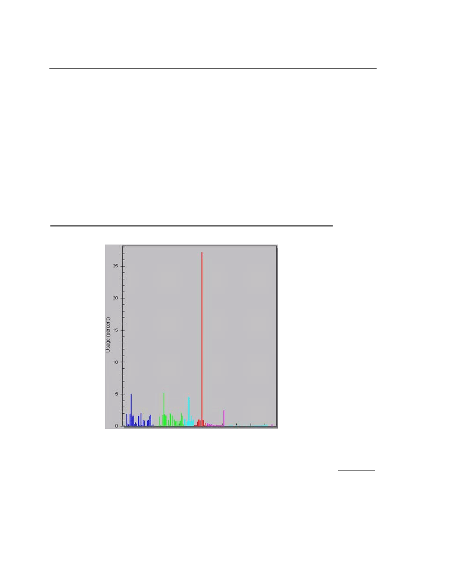
Application Performance Tools
7
7-3
The time-based sampling (TBS) periodically interrupts the processor at the
specified sampling interval and collects samples of the instruction
addresses, matches these addresses with an application or an operating
system routine, and creates a database with the resulting samples data.
VTune analyzer can then graphically display the amount of CPU time spent
in each active module, process, and processor (on a multiprocessor system).
The TBS—
•
samples and display a system-wide view of the CPU time distribution
of all the software activity during the sampling session
•
determines which sections in your code are taking the most CPU time
•
analyzes hotspots, displays the source code, and determines
performance issues at the source and assembly code levels.
Figure 7-1 provides an example of a hotspots report by location.
Figure 7-1
Sampling Analysis of Hotspots by Location
_____________________________________________________________

7-4
7
Intel Architecture Optimization Reference Manual
Event-based Sampling
You can use event-based sampling (EBS) to monitor all active software on
your system, including the operating system, device drivers, and application
software based on the occurrence of processor events.
The VTune analyzer collects, analyzes, and displays the performance event
counters data of your code provided by the Pentium
®
II and Pentium
III
processors. These processors can generate numerous events per clock cycle.
The VTune analyzer supports the events associated with counter 0 only.
For event-based sampling, you can select one or more events, in each event
group. However, the VTune analyzer runs a separate session to monitor
each event you have selected. It interrupts the processor after a specified
number of events and collects a sample containing the current instruction
address. The frequency at which the samples are collected is determined by
how often the event is caused by the software running in the system during
the sampling session.
The data collected allows you to determine the number of events that
occurred and the impact they had on performance. Sampling results are
displayed in the Modules report and Hotspots report. Event data is also
available as a performance counter in the Chronologies window. The event
sampled per session is listed under the Chronologies entry in the Navigation
tree of the VTune analyzer.
Sampling Performance Counter Events
Event-based sampling can be used together with the hardware performance
counters available in the Intel architecture to provide detailed information
on the behavior of specific events in the microprocessor. Some of the
microprocessor events that can be sampled include L2 cache misses, branch
mispredictions, misaligned data access, processor stalls, and instructions
executed.
VTune analyzer provides access to the performance counters listed in
Appendix B, “
Performance-Monitoring Events and Counters
processors' performance counters can be configured to monitor any of
several different types of events. All the events are listed in the Configure
menu/Options command/Processor Events for EBS page of the VTune
analyzer, see Figure 7-2.
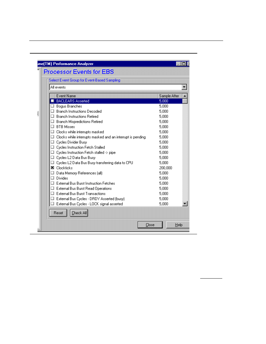
Application Performance Tools
7
7-5
At first glance, it is difficult to know which counters are relevant for
understanding the performance effects. For example, to better understand
performance effects on the cache and bus behavior with the Pentium
III
Figure 7-2
Processor Events List

7-6
7
Intel Architecture Optimization Reference Manual
processor, the VTune analyzer collected the performance data with and
without the prefetch and streaming store instructions. The main counters
that relate to the activity of the system bus, as well as the cache hierarchy
include:
•
L1 cache misses—this event indicates the number of outstanding L1
cache misses at any particular time.
•
L2 cache misses—this event indicates all data memory traffic that
misses the L2 cache. This includes loads, stores, locked reads, and
ItoM requests.
•
L2 cache requests—this event indicates all L2 cache data memory
traffic. This includes loads, stores, locked reads, and ItoM requests.
•
Data memory references—this event indicates all data memory
references to the L1 data and instruction caches and to the L2 cache,
including all loads from and to any memory types.
•
External bus memory transactions—this event indicates all memory
transactions.
•
External bus cycles processor busy receiving data—VTune analyzer
counts the number of bus clock cycles during which the processor is
busy receiving data.
•
External bus cycles DRDY asserted—this event indicates the number
of clocks during which DRDY is asserted. This, essentially, indicates
the utilization of the data bus.
Other counters of interest are:
•
Instructions retired—this event indicates the number of instructions
that retired or executed completely. This does not include partially
processed instructions executed due to branch mispredictions.
•
Floating point operations retired—this event indicates the number of
floating point computational operations that have retired.
•
Clockticks—this event initiates time-based sampling by setting the
counters to count the processor's clock ticks.
•
Resource-related stalls—this event counts the number of clock cycles
executed while a resource-related stall occurs. This includes stalls due
to register renaming buffer entries, memory buffer entries, branch
misprediction recovery, and delay in retiring mispredicted branches.
•
Prefetch NTA—this event counts the number of Streaming SIMD
Extensions
prefetchnta
instructions.

Application Performance Tools
7
7-7
The raw data collected by the VTune analyzer can be used to compute
various indicators. For example, ratios of the clockticks, instructions retired,
and floating-point instructions retired can give you a good indication as to
which parts of applications are best suited for a potential re-coding with the
Streaming SIMD Extensions.
Call Graph Profiling
The call graph profiles your applications and displays a call graph of active
functions. The call graph analyzes the data and displays a graphical view of
the threads created during the execution of the application, a complete list of
the functions called, and the relationship between the parent and child
functions. Use VTune analyzer to profile your Win32* executable files or
Java* applications and generate a call graph of active functions.
Call graph profiling includes collecting and analyzing call-site information
and displaying the results in the Call List of the Call Graph and Source
views. The call graph profiling provides information on how many times a
function (caller) called some other function (callee) and the amount of time
each call took. In many cases the caller may call the callee from several
places (sites), so call graph also provides call information per site. (Call site
information is not collected for Java call graphs.)
The View by Call Sites displays the information about callers and callees of
the function in question (also referred to as current function) by call sites.
This view allows you to locate the most expensive calls.
Call Graph Window
The call graph window comprises three views: Spreadsheet, Call Graph, and
Call List, see Figure 7-3. The Call Graph view, displayed on the lower
section of the window, corresponds to the function (method) selected in the
Spreadsheet. It displays the function, the function’s parents, and function’s
child functions.
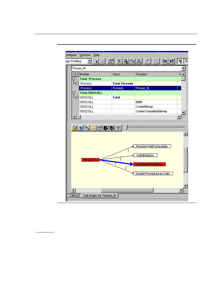
7-8
7
Intel Architecture Optimization Reference Manual
Figure 7-3
Call Graph Window

Application Performance Tools
7
7-9
Each node (box) in the call graph represents a function. Each edge (line
with an arrow) connecting two nodes represents the call from the parent
(caller) to the child function (callee). The number next to the edge (line)
indicates the number of calls to that function.
The window has a Call List tab in the bottom of the Call Graph view. The
Call List view lists all the callers and the callees of the function selected in
the spreadsheet and displayed in the Call Graph view. In addition, the Call
List has a View by Call Sites in which you can see call information
represented by call sites.
Static Code Analysis
This feature analyzes performance through
•
performing static code analysis of the functions or blocks of code in
your application without executing your application
•
getting a list of functions with their respective addresses for quick
access to your code
•
getting summary information about the percentage of pairing and
penalties incurred by the instructions in each function.
The static code analyzer provides analysis of the instructions in your
application and their relationship with each other, without executing or
sampling them. It provides an estimation of the performance of your
application, not actual performance. The static code analyzer analyzes the
module you specified in the Executable field and displays the results. By
default, the static code analyzer analyzes only those functions in the module
that have source code available.
During the static code analysis, the static code analyzer does the following
tasks:
•
searches your program for the debug symbols or prompts you to
specify the symbol files
•
searches the source directories for the source files
•
analyzes each basic block and function in your program
•
creates a database with the results

7-10
7
Intel Architecture Optimization Reference Manual
•
displays summary information about the performance of each function,
including its name, address, the number of instructions executed, the
percentage of pairing, the total clock cycles incurred, and the number
of clock cycles incurred due to penalties.
Static Assembly Analysis
This feature of the VTune analyzer determines performance issues at the
processor level, including the following:
•
how many clocks each instruction takes to execute and how many of
them were incurred due to penalties
•
how your code is executing in the three decode units of the Pentium II
and Pentium
III
processors
•
regardless of the processor your system is using, the static assembly
analyzer analyzes your application’s performance as it would run on
Intel processors, from Intel486™ to Pentium
III
processors.
The VTune analyzer’s static assembly analyzer analyzes basic blocks of
code. It assumes that the code and data are already in the cache and ignores
loops and jumps. It disassembles your code and displays assembly
instructions, annotated with performance information.
The static assembly analyzer disassembles hotspots or static functions in
your Windows 95, 98 and NT binary files and analyzes architectural issues
that effect their performance. You can invoke Static Assembly Analysis
view either by performing a static code analysis or by time or event-based
sampling of your binary file. Click on the View Static Assembly Analysis
icon in the VTune analyzer’s toolbar to view a static analysis of your code
and display the assembly view.
Dynamic Assembly Analysis
Dynamic assembly analysis fine-tunes sections of your code and identifies
the exact instructions that cause critical performance problems. It simulates
a block of code and discovers such events as missed cache accesses,
renaming stalls, branch target buffer (BTB) misses, and misaligned data that
can degrade performance on Intel architecture-based processors.
Dynamic analysis gives you precise data about the behavior of the cache
and BTB by simulating the inner-workings of Intel’s super-scalar,
out-of-order micro-architecture. The dynamic assembly analyzer executes

Application Performance Tools
7
7-11
the application, traces its execution, simulates, and monitors the
performance of the code you specify. You can perform dynamic analysis
using three different simulation methods:
•
Selected code
•
Uniform sampling
•
Start and stop API
These methods provide alternate ways of filtering data and focusing on
critical sections of code. They differ in the way they invoke dynamic
analysis, simulate and analyze specific instructions, and in the amount of
output they display. For example, in the selected code method, the dynamic
assembly analyzer analyzes and displays output for every instruction within
a selected range, while in the uniform sampling and start/stop API
simulation methods, only the critical sections of code are simulated and
analyzed.
Code Coach Optimizations
The code coach performs the following:
•
Analyzes C, FORTRAN, C++, and Java* source code and produces
high-level source code optimization advice.
•
Analyzes assembly code or disassembled assembly code and produces
assembly instruction optimization advice.
Once the VTune analyzer identifies, analyzes, and displays the source code
for hotspots or static functions in your application, you can invoke the coach
for advice on how to rewrite the code to optimize its performance.
Typically, a compiler is restricted by language pointer semantics when
optimizing code. Coach suggests source-level modifications to overcome
these and other restrictions. It recognizes commonly used code patterns in
your application and suggests how they can be modified to improve
performance. The coach window is shown in Figure 7-4.
You can invoke the coach from the Source View window by double-
clicking on a line of code, or selecting a block of code and then clicking on
the code coach icon on the Source View toolbar.
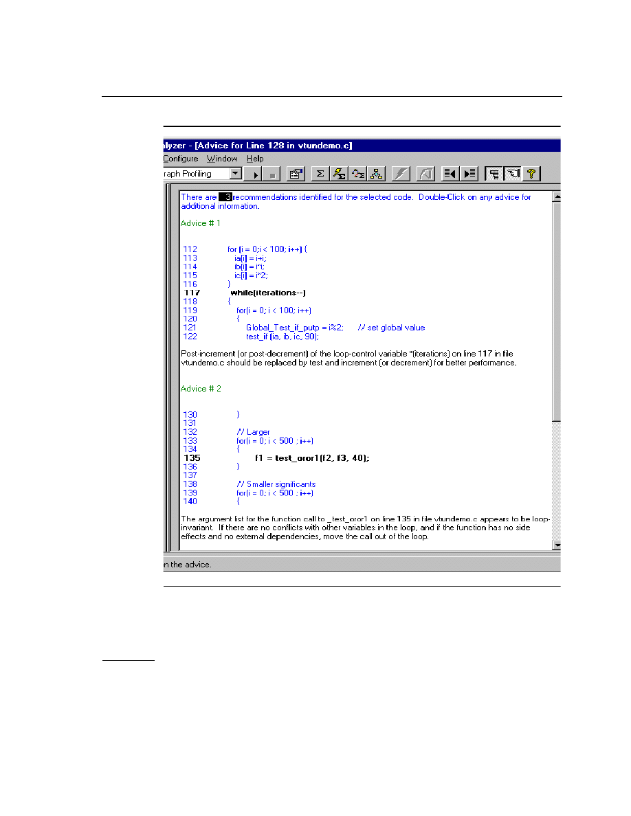
7-12
7
Intel Architecture Optimization Reference Manual
Figure 7-4
Code Coach Optimization Advice

Application Performance Tools
7
7-13
The coach examines the entire block of code or function you selected and
searches for optimization opportunities in the code. As it analyzes your
code, it issues error and warning messages much like a compiler parser.
Once the coach completes analyzing your code, if it finds suitable
optimization advice, it displays the advice in a separate window.
The coach may have more than one advice for a loop or function. If no
advice is available, it displays an appropriate message. You can double-
click on any advice in the coach window to display context-sensitive help
with examples of the original and optimized code.
Where performance can be improved using MMX technology or Streaming
SIMD Extensions
intrinsics, the coach provides advice in the form of
C-style pseudocode, leaving the data definitions, loop control, and
subscripts to the programmer.
For the code using the intrinsics, you can double-click the left mouse button
on an argument used in the code to display the description of that argument.
Click your right mouse button on an intrinsic to invoke a brief description of
that intrinsic.
Assembly Coach Optimization Techniques
Assembly coach uses many optimization techniques to produce its
recommended optimized code, for example:
•
Instruction Selection—assembly coach analyzes each instruction in
your code and suggests alternate, equivalent replacements that are
faster or more efficient.
•
Instruction Scheduling—assembly coach uses its in-depth knowledge
of processor behavior to suggest an optimal instruction sequence that
preserves your code's semantics.
•
Peephole Optimization—assembly coach identifies particular
instruction sequences in your code and replaces them with a single,
equivalent instruction.
•
Partial Register Stall Elimination—assembly coach identifies
instruction sequences that can produce partial register stalls and
replaces them with alternative sequences that do not cause partial stalls.

7-14
7
Intel Architecture Optimization Reference Manual
In Automatic Optimization and Single Step Optimization modes, you can
select or deselect these optimization types in the Assembly Coach Options
tab.
Intel Compiler Plug-in
The Intel C/C++ compiler is compatible with Microsoft Visual C++* and is
available as a plug-in to the Microsoft Developer Studio IDE.
Intel C/C++ compiler allows you to optimize your code by using special
optimization command-line options described in this section.
The optimization command-line options generally are
-01
and
-02
. Each of
them enables a number of specific optimization options. In most cases,
-O2
is recommended over
-O1
because the
-O2
option enables inline
expansion, which helps programs that have many function calls. The
O2
option is on by default.
The
-01
and
-02
options enable the options as follows:
-O1
Enables options
-Og
,
-Oi-
,
-Os
,
-Oy
,
-Ob1
,
-Gf
,
-Gs
, and
-Gy
. However,
-O1
disables a few options
that increase code size.
-O2
Enables options
-Og
,
-Oi
,
-Ot
,
-0y
,
-Ob1
,
-Gf
,
-Gs
,
and
-Gy
. Confines optimizations to the
procedural level.
All the command-line options are described in the Intel C/C++ Compiler
User’s Guide for Win32 Systems, order number 718195.
The
-0d
option disables optimization. You can specify optimization option
as “
any
” instead of
-01
or
-02
. This is the only optimization not disabled
by
-Od
.
Code Optimization Options
This section describes the options used to optimize your code and improve
the performance of your application.

Application Performance Tools
7
7-15
Targeting a Processor (
-G
n
)
Use
-G
n
to target an application to run on a specific processor for maximum
performance. Any of the
-G
n
suboptions you choose results in your binary
running on a corresponding Intel architecture 32-bit processors.
-G6
is the
default, and targets optimization for the Pentium II and Pentium
III
processors.
Automatic Processor Dispatch Support (
-Qx
[extensions]
and
-Qax
[extensions]
)
The
-Qx
[extensions]
and
-Qax
[extensions]
options provide
support to generate code that is specific to processor-instruction extensions.
-Qx
[extensions]
generates specialized code to run exclusively on the
processors indicated by the extension.
-Qax
[extensions]
generates code specialized to the specified
extensions, but also generates generic IA-32 code.
The generic code is usually slower. A runtime check
for the processor type is made to determine which
code executes.
You can specify the same extensions for either option as follows:
i
Pentium II and Pentium
III
processors, which use the
CMOV
and
FCMOV
instructions
M
Pentium II and Pentium
III
processors
K
Streaming SIMD Extensions, which include the
i
and
M
extensions.
CAUTION.
When you use
-Qax[extensions]
in conjunction with
-Qx[extensions],
the extensions specified by
-Qx[extensions]
can be used unconditionally by the compiler, and the resulting program
will require the processor extensions to execute properly.

7-16
7
Intel Architecture Optimization Reference Manual
Vectorizer Switch Options
The Intel C/C++ Compiler can vectorize your code using the vectorizer
switch options. The option that enables the vectorizer is
-Qvec
. The
compiler provides a number of other vectorizer switch options that allow
you to control vectorizations. All vectorization switches require the
-Qvec
switch to be on. The default is off.
The vectorizer switch options can be activated from the command line. In
addition to the
-Qvec
switch, the compiler provides the following
vectorization control switch options:
-Qvec_alignment
Controls the default alignment of vectorizable
data.
-Qvec_verbose
Controls the vectorizer’s diagnostic levels.
-
Qrestrict
Enables pointer disambiguation with the
restrict
qualifier
.
-Qkscalar
Performs all 32-bit floating point arithmetic using
the Streaming SIMD Extensions instead of the
default x87 instructions.
-Qvec_emms[-]
Controls the automation of EMMS instruction
insertions to empty the MMX instruction
registers.
-Qvec_no_arg_alias[-]
Assumes on entry that procedure arguments are
not aliased.
-Qvec_no_alias[-]
Assumes that no aliasing can occur between
objects with different names.
Prefetching (
-Qpf
[options]
)
Use
-Qpf
to automatically insert prefetching on a Pentium
III
processor.
This option enables three suboptions (
-Qpf_loop
,
-Qpf_call
, and
-Qpf_sstore
) each of which improves cache behavior. The following
example invokes
-Qpf
as one option with all its functionality:
prompt>
icl -Qpf prog.cpp

Application Performance Tools
7
7-17
Loop Unrolling (
-Qunroll
n
)
Use
-Qunroll
n
to specify the maximum number of times you want to
unroll a loop. For example, to unroll a loop at most four times, use this
command:
prompt>
icl -Qunroll4 a.cpp
To disable loop unrolling, specify
n
as
0
.
Inline Expansion of Library Functions (
-Oi
,
-Oi-
)
The compiler inlines a number of standard C, C++, and math library
functions by default. This usually results in faster execution of your
program. Sometimes, however, inline expansion of library functions can
cause unexpected results. For explanation, see Intel C/C++ Compiler
User’s Guide for Win32 Systems, order number 718195.
Floating-point Arithmetic Precision (
-Op
,
-Op-
,
-Qprec
,
-Qprec_div
,
-Qpc
,
-Qlong_double
)
These options provide optimizations with varying degrees of precision in
floating-point arithmetic.
Rounding Control Option (
-Qrcd
)
The compiler uses the
-Qrcd
option to improve the performance of code
that requires floating point calculations. The optimization is obtained by
controlling the change of the rounding mode.
The
-Qrcd
option disables the change to truncation of the rounding mode
in floating point-to-integer conversions.
For complete details on all of the code optimization options, refer to the
Intel C/C++ Compiler User’s Guide for Win32 Systems, order number
718195.
Interprocedural and Profile-Guided Optimizations
The following are two methods to improve the performance of your code
based on its unique profile and procedural dependencies:
Interprocedural Optimization (IPO)—Use the
-Qip
option to analyze
your code and apply optimizations between procedures within each source
file. Use multifile IPO with
-Qipo
to enable the optimizations between
procedures in separate source files.

7-18
7
Intel Architecture Optimization Reference Manual
Use the
-Qoption
suboption with the applicable keywords to select
particular in-line expansions and loop optimizations. If you specify
-Qip
without the
-Qoption
qualification, the compiler expands functions in line,
propagates constant arguments, passes arguments in registers, and monitors
module-level static variables.
Profile-Guided Optimization (PGO)—Creates an instrumented program
from your source code and special code from the compiler. Each time this
instrumented code is executed, the compiler generates a dynamic
information file. When you compile a second time, the dynamic information
files are merged into a summary file. Using the profile information in this
file, the compiler attempts to optimize the execution of the most heavily
travelled paths in the program.
When you use PGO, consider the following guidelines:
•
Minimize the changes to your program after instrumented execution
and before feedback compilation. During feedback compilation, the
compiler ignores dynamic information for functions modified after that
information was generated.
•
Repeat the instrumentation compilation if you make many changes to
your source files after execution and before feedback compilation.
For complete details on the interprocedural and profile-guided
optimizations, refer to the Intel C/C++ Compiler User’s Guide for Win32
Systems, order number 718195.
Intel Performance Library Suite
The Intel Performance Library Suite (PLS) includes the following libraries:
•
The Intel Signal Processing Library: set of signal processing functions
similar to those available for most Digital Signal Processors (DSPs)
•
The Intel Recognition Primitives Library, a set of 32-bit recognition
primitives for developers of speech- and character-recognition software
NOTE.
The compiler issues a warning that the dynamic information
corresponds to a modified function.

Application Performance Tools
7
7-19
•
The Intel Image Processing Library, a set of low-level image
manipulation functions particularly effective at taking advantage of
MMX technology
•
The Intel Math Kernel Library, a set of linear algebra and fast Fourier
transform functions for developers of scientific programs.
•
The Intel Image Processing Primitives: a collection of low-overhead
versions of common functions on 2D arrays intended as a supplement
or alternative to the Intel Image Processing Library.
Benefits Summary
The overall benefits the libraries provide to the application developers are as
follows:
•
Low-level functions for multimedia applications
•
Highly-optimized routines with a C interface, “no assembly required”
•
Processor-specific optimization
•
Processor detection and DLL dispatching
•
Pure C version for any IA processor
•
Custom DLL builder for reduced memory footprint
•
Built-in error handling facility
The libraries are optimized for all Intel architecture-based processors. The
custom DLL builder allows your application to include only the functions
required by the application.
Libraries Architecture
Each library in the Intel Performance Library Suite implements specific
architecture that ensures high performance. The Signal Processing Library
(SPL), the Recognition Primitives Library (RPL), and the Math Kernel
Library (MKL) use the data types such as signed and unsigned short
integers, output scale or saturation mode, and single and double-precision
floats. The bulk of the functions support real and complex functions. All
these features ensure fast internal computations at higher precision.
The Image Processing Library (IPL) implements specific image processing
techniques such as bit depths, multiple channels, data alignment, color
conversion, region of interest and tiling. The region of interest (ROI) defines

7-20
7
Intel Architecture Optimization Reference Manual
a particular area within entire image and enables you to perform operations
on it. Tiling is a technique that handles large images by diving an image into
sub-blocks.
The Image Processing Primitives (IPP) library is a collection of
high-performance operations performed on 1D and 2D arrays of pixels. The
IPP provides lower-overhead versions of common functions on 2D arrays
and is intended as a supplement or alternative to the Intel Image Processing
Library.
The Math Kernel Library (MKL) is most helpful for scientific and
engineering applications. Its high-performance math functions include
Basic Linear Algebra Subprograms (BLAS) and fast Fourier transforms
(FFTs) that run on multiprocessor systems. No change of the code is
required for multiprocessor support. The library is threadsafe and shows the
best results when compiled by the Intel compiler.
All libraries employ complicated memory management schemes and
processor detection.
Optimizations with Performance Library Suite
The PLS implements a number of optimizations discussed throughout this
manual, including architecture-specific tuning such as loop unrolling,
instructions pairing and instructions scheduling; memory managing such as
prefetching and cache tuning.
The library suite focuses on taking advantage of the parallelism of the
SIMD instructions that comprise the MMX technology and Streaming
SIMD Extensions. This technique improves the performance of
computationally intensive image processing functions. Thus the PLS
includes a set of functions whose performance significantly improves when
used with the Intel architecture processors. In addition, the libraries use
table look-up techniques and fast Fourier transforms (FFTs).
The PLS frees the application developers from assembly programming for
the variety of frequently used functions and prepares the programs for the
new processor since the libraries are capable of detecting the processor type,
including the future processors, and adjusting the code accordingly.

Application Performance Tools
7
7-21
Register Viewing Tool (RVT)
The Register Viewing Tool (RVT) for Windows 95, 98, and Windows NT
allows you to directly view the contents of the Streaming SIMD Extensions
registers without using a debugger. In addition, the RVT provides
disassembly information during debug for Streaming SIMD Extensions.
This capability of viewing the contents of registers without using debugger
is the contribution of the RVT to optimizing your application. For complete
details, refer to the Register Viewing Tool, version 4.0 online help.
Register Data
The RVT displays the contents of the Streaming SIMD Extensions registers
in an RVT Display window. The contents of the eight Streaming SIMD
Extensions registers, XMM0 through XMM7 fields are displayed in one of
four formats: byte (16 bytes), word (8 words), dword (4 doublewords) or
single (4 single words in floating-point format). The RVT allows you to set
the format as you need. The new value appears in red.
The window displays the trapped code segment register and the trapped
extended instruction pointer. The window has a First Byte Field which
allows you to enter the first byte value of the break-point command when a
break point is reached. From the RVT display window, you can call the
Disassembly window.
Disassembly Data
In a debug mode, the disassembly window displays the full disassembly of
the current EIP address plus 40 bytes of disassembly information before and
after the current EIP. This information is shown after every debug
breakpoint or single-step depending on how you set your debug
environment, see Figure 7-5.
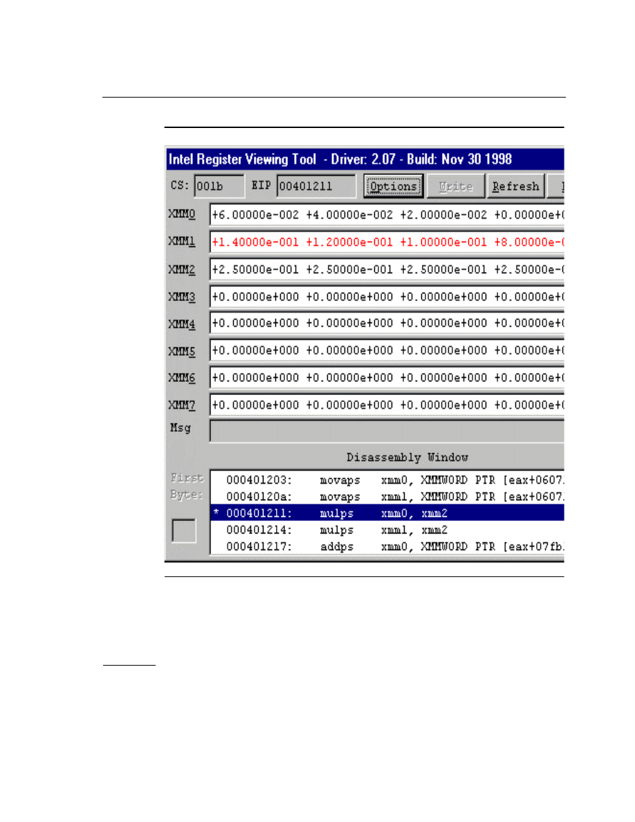
7-22
7
Intel Architecture Optimization Reference Manual
Figure 7-5
The RVT: Registers and Disassembly Window

Application Performance Tools
7
7-23
To ensure accurate disassembly information at a breakpoint, you need to
enter the correct first byte value of the break-point command from the RVT
display window. The RVT uses information from memory which
remembers the value that you enter within a loop from one iteration to the
next, up to 20 LRU first bytes. Synchronization of the RVT and the
instructions occurs at the current EIP.


A-1
Optimization of Some Key
Algorithms for the
Pentium
®
III
Processors
A
The MMX™ technology and Streaming SIMD Extensions for the Intel
®
architecture (IA) instruction set provides single-instruction, multiple-data
(SIMD) floating-point instructions and SIMD integer instructions. These
instructions, in their turn, provide a means to accelerate operations typical
of 3D graphics, real-time physics, spatial (3D) audio, and others.
This appendix describes several key algorithms and their optimization for
the Pentium
®
III
processors. The algorithms discussed are:
•
Using Newton-Raphson Method with the reciprocal (
rcpps
) and
reciprocal square root (
rsqrtps
) instructions.
•
Using
prefetch
instruction for transformation and lighting operations
to reduce memory load latencies.
•
Using the packed sum of absolute differences instruction (
psadbw
) to
implement a fast motion-estimation error function.
•
Using MMX technology and Streaming SIMD Extensions intrinsics
and vector classes for any sequential sample stream either to increase
or reduce the number of samples.
•
Using Streaming SIMD Extensions technology intrinsics and vector
classes for both real and complex 16-tap finite duration impulse
response (FIR) filter.

A-2
A
Intel Architecture Optimization Reference Manual
Newton-Raphson Method with the Reciprocal
Instructions
The Newton-Raphson formula for finding the root of an equation is
:
where
x
i
is the estimated root
f(x
i
)
is the function evaluated at the root estimate
f*(x
i
)
is the first derivative of the function evaluated at the root
estimate.
The Newton-Raphson method is the preferred method for finding the root of
functions for which the derivative can be easily evaluated and for which the
derivative is continuous and non-zero in the neighborhood of the root. The
Newton-Raphson method approximately doubles the number of significant
digits for each iteration if the initial guess is close to the root.
The Newton-Raphson method is used to increase the accuracy of the results
for the reciprocal (
rcpps
) and the reciprocal square root (
rsqrtps
)
instructions. The
rcpps
and
rsqrtps
instructions return a result, which is
accurate in the 12 most significant bits of the mantissa. These two
instructions have a 3-cycle latency opposed to 26 cycles required to use the
divide instruction.
In some algorithms, it may be desirable to have full accuracy while realizing
the performance benefit of using the approximation instructions. The
method illustrated in the examples yields near full accuracy, and provides a
sizable performance gain compared to using the divide or square root
functions. One iteration of the Newton-Raphson method is sufficient to
produce a result which is accurate to 23 of 24 bits for single precision
numbers (24 bits includes the implied “1” before the binary point).
For complete details, see the Increasing the Accuracy of the Results from the
Reciprocal and Reciprocal Square Root Instructions using the
Newton-Raphson Method, Intel application note, order number 243637.
x
i
1
+
x
i
f x
i
( )
f
∗
x
i
( )
--------------
–
=

Optimization for Some Key Algorithms for the Pentium III Processors
A
A-3
Performance Improvements
For the ASM versions, the approximation instruction (
rcpps
) and the
reciprocal square root instruction (
rsqrtps
) by themselves are 1.8 and
1.6
times, respectively, faster than implementing the Newton-Raphson method.
It is important to investigate whether the extra accuracy is required before
using the Newton-Raphson method to insure that the maximum
performance is obtained. If full accuracy is required, then the
Newton-Raphson method provides a 12 times increase for the reciprocal
approximation and 35 times for the reciprocal square root approximation
over C code, and over a 3.3 times and 9.6 times increase above the SIMD
divide instruction, respectively for each operation.
Unrolling the loops further enhances performance. After unrolling, the code
was scheduled to hide the latency of the multiplies by interleaving any
non-dependent operations. The gain in performance for unrolling the
reciprocal code was due to reduced instructions (55%) and scheduling
(45%). The gain in performance for unrolling the reciprocal square root
code was due to reduced instructions (30%) and scheduling (70%).
Newton-Raphson Method for Reciprocal Square Root
Example A-1 demonstrates a Newton-Raphson approximation for
reciprocal square root operation implemented with inlined assembly for the
Streaming SIMD Extensions, the intrinsics, and the F32vec4 class. The
complete sample program, including the code for the accurate
Newton-Raphson Methods can be found in the
VTuneEnv\Samples\NRReciprocal
directory of the VTune
Performance Enhancement Environment CD, version 4.0.

A-4
A
Intel Architecture Optimization Reference Manual
Example A-1 Newton-Raphson Method for Reciprocal Square Root
Approximation
void RecipSqRootApproximationASM(float * lpfInput, float *
lpfRecipOutput, int iNumToDo)
{
__asm
{
mov esi, lpfInput
mov edi, lpfRecipOutput
mov ecx, iNumToDo
shr ecx, 2 ; divide by 4, do 4 at a time
Invert:
movaps xmm0, [esi]
add edi, 16
rsqrtps xmm1, xmm0
add esi, 16
movaps [-16][edi], xmm1
dec ecx
jnz Invert
}
}
void RecipSqRootApproximationIntrinsics(float * lpfInput, float *
lpfRecipOutput, int iNumToDo)
{
int i;
__m128 *In, *Out;
In = (__m128 *) lpfInput;
Out = (__m128 *) lpfRecipOutput;
iNumToDo /= 4; ; divide # to do by 4 since we are
; doing 4 with each intrinsic
for(i = 0; i < iNumToDo; i ++)
{
*Out++ = _mm_rsqrt_ps(*In++);
}
}
_________________________________________________________________________
continued

Optimization for Some Key Algorithms for the Pentium III Processors
A
A-5
Example A-1 Newton-Raphson Method for Reciprocal Square Root
Approximation (continued)
void RecipSqRootApproximationF32vec4(float * lpfInput, float *
lpfRecipOutput, int iNumToDo)
{
int i;
F32vec4 *In, *Out;
In = (F32vec4 *) lpfInput;
Out = (F32vec4 *) lpfRecipOutput;
for(i = 0; i < iNumToDo; i += 4)
{
*Out++ = rsqrt(*In++);
}
}
_________________________________________________________________________
Newton-Raphson Inverse Reciprocal Approximation
Example A-2 demonstrates Newton-Raphson method for inverse reciprocal
approximation using inlined assembly for the Streaming SIMD Extensions,
the intrinsics, and the F32vec4 class. The complete sample program,
including the code for the accurate Newton-Raphson Methods can be found
in the
VTuneEnv\Samples\NRReciprocal
directory of the VTune™
Performance Enhancement Environment CD, version 4.0.
Example A-2 Newton-Raphson Inverse Reciprocal Approximation
void RecipApproximationASM(float * lpfInput, float * lpfRecipOutput,
int iNumToDo)
{
__asm
{
mov
esi, lpfInput
_________________________________________________________________________
continued

A-6
A
Intel Architecture Optimization Reference Manual
Example A-2 Newton-Raphson Inverse Reciprocal Approximation (continued)
mov
edi, lpfRecipOutput
mov
ecx, iNumToDo
shr
ecx, 4
; divide by 16, do 16 at a time
Invert:
movaps mm0, [esi]
add
edi, 64
movaps xmm2, [16][esi]
movaps xmm4, [32][esi]
movaps xmm6, [48][esi]
add esi, 64
rcpps xmm1, xmm0
rcpps xmm3, xmm2
rcpps xmm5, xmm4
rcpps xmm7, xmm6
movaps [-64][edi], xmm1
movaps [-48][edi], xmm3
movaps [-32][edi], xmm5
dec ecx
movaps [-16][edi], xmm7
jnz Invert
}
}
void RecipApproximationIntrinsics(float * lpfInput, float *
lpfRecipOutput, int iNumToDo)
{
int i;
__m128 *In, *Out;
_________________________________________________________________________
continued

Optimization for Some Key Algorithms for the Pentium III Processors
A
A-7
Example A-2 Newton-Raphson Inverse Reciprocal Approximation (continued)
In = (__m128 *) lpfInput;
Out = (__m128 *) lpfRecipOutput;
iNumToDo = iNumToDo >> 2;
; divide # to do by 4 since we
; are doing 4 with each intrinsic
for(i = 0; i < iNumToDo; i ++)
{
*Out++ = _mm_rcp_ps(*In++);
}
}
void RecipApproximationF32vec4(float * lpfInput, float *
lpfRecipOutput, int iNumToDo)
{
int i;
F32vec4 *In, *Out;
In = (F32vec4 *) lpfInput;
Out = (F32vec4 *) lpfRecipOutput;
iNumToDo = iNumToDo >> 2;; divide by 4, do 4 at a time
for(i = 0; i < iNumToDo; i ++)
{
*Out++ = rcp(*In++);
}
}
_________________________________________________________________________
3D Transformation Algorithms
The examples of 3D transformation operations algorithms in this section
demonstrate how to write efficient code with Streaming SIMD Extensions.
The purpose of these algorithms is to make the transformation and lighting

A-8
A
Intel Architecture Optimization Reference Manual
operations work together efficiently and to use new
prefetch
instructions
to reduce memory load latencies. The performance of code using the
Streaming SIMD Extensions is around three times better than the original C
code.
For complete details, refer to the Streaming SIMD Extensions -- 3D
Transformation, Intel application note, order number 243831.
Aos and SoA Data Structures
There are two kinds of data structures: the traditional Array of Structures
(AoS), with data organized according to vertices - x
0
y
0
z
0
, and the
Structure of Arrays (SoA), with data organized according to coordinates -
x
0
x
1
x
2
x
3
. The SoA data structure is a more natural structure for SIMD
instructions.
The best performance is achieved by performing the transformation with
data in SoA format. However some applications require the data in AoS
format. In these cases it is still possible to use Streaming SIMD Extensions,
by transposing the data to SoA format before the transformation and
lighting operations. After these operations are complete, de-transpose the
data back to AoS format.
Performance Improvements
The performance improvements for the 3D transform algorithms can be
achieved by
•
using SoA structures
•
prefetching data
•
avoiding dependency chains
SoA
The Streaming SIMD Extensions enable increased performance over scalar
floating-point code, through utilizing the SIMD feature of these
instructions. When the data is arranged in SoA format, one instruction
handles four data elements. This arrangement also eliminates loading data
that is not relevant for the transformation, such as texture coordinates, color,
and spectral information.

Optimization for Some Key Algorithms for the Pentium III Processors
A
A-9
Prefetching
Additional performance gain is achieved by prefetching the data from main
memory, and by replacing the long latency
divps
instruction with a low
latency
rcpps
instruction, or its Newton-Raphson approximation for better
precision. For more information, see the
section earlier in this appendix. For complete
details, refer to the Increasing the Accuracy of the Results from the
Reciprocal and Reciprocal Square Root Instructions using the
Newton-Raphson Method, Intel application note, order number 243637.
Avoiding Dependency Chains
Yet another performance increase can be obtained by avoiding writing code
that contains chains of dependent calculations. The dependency problem
can occur with the
movhps/movlps/shufps
sequence, since each
movhps/movlps
instruction bypasses part of the destination register. These
instructions cannot execute until prior instructions that generate the
corresponding register are completed. This dependency can prevent
successive loop iterations from executing in parallel.
One solution to this problem is to include a 128-bit load from a dummy
local variable to each register used with a
movhps
/
movlps
instruction. This
effectively breaks dependency by performing an independent load from a
memory or cached location. In some cases, such as loading a section of a
transform matrix, the code that uses the swizzled results already includes
128-bit loads. In these cases, an additional explicit 128-bit dummy load is
not required.
Implementation
The code examples, including a sample program using the techniques
described above can be found in the
\VTuneEnv\Samples\3DTrans\aos
and
\VTuneEnv\Samples\3DTrans\soa
directories of the VTune
Performance Enhancement Environment, version 4.0. Example A-3 shows
the code for the transformation algorithm for the SoA version implemented
in scalar C, and the intrinsics and vector class for the Streaming SIMD
Extensions.

A-10
A
Intel Architecture Optimization Reference Manual
Example A-3 Transform SoA Functions, C Code
void TransformProjectSoA(VerticesList *inp, VerticesList *out, int
count, camera *cam)
{
int i;
float x,y,z;
float orw;
for (i=0; i<count; i++){
x = inp->x[i], y = inp->y[i], z = inp->z[i];
orw = x * mat->_30 + y * mat->_31 + z * mat->_32 +
mat->_33;
out->x[i] = (x*mat->_00 + y*mat->_01 + z*mat->_02 +
mat->_03)*(cam->sx/orw)
+
cam->tx;
out->y[i] = (x*mat->_10 + y*mat->_11 + z*mat->_12 +
mat->_13)*(cam->sy/orw) + cam->ty;
out->z[i] = (x*mat->_20 + y*mat->_21 + z*mat->_22 +
mat->_23)*(cam->sz/orw) + cam->tz;
out->w[i] = orw;
}
}
//-----------------------------------------------------------------
// This version uses the intrinsics for the Streaming SIMD
Extensions.
// Note that the F32vec4 can be used in place of __m128 variables as
// operands to the intrinsics.
//-----------------------------------------------------------------
void TransformProjectSoAXMMIntrin(VerticesListV *inp, VerticesListV
*out, int count, camera *cam)
{
int i;
F32vec4 x, y, z;
F32vec4 orw;
F32vec4 SX=cam->sx, SY=cam->sy, SZ=cam->sz;
F32vec4 TX=cam->tx, TY=cam->ty, TZ=cam->tz;
_________________________________________________________________________
continued

Optimization for Some Key Algorithms for the Pentium III Processors
A
A-11
Example A-3 Transform SoA Functions, C Code (continued)
for (i=0; i<count/VECTOR_SIZE; i++){
x = inp->x[i], y = inp->y[i], z = inp->z[i];
// orw = x * mat30 + y * mat31 + z * mat32 + mat33;
orw = (_mm_add_ps(
_mm_add_ps(
_mm_mul_ps(x, mat30),
_mm_mul_ps(y, mat31)),
_mm_add_ps(
_mm_mul_ps(z, mat32),
mat33)));
// out->x[i] = (x*mat->_00 + y*mat->_01 + z*mat->_02 +
mat->_03)*(cam->sx/orw) + cam->tx;
out->x[i] = (_mm_add_ps(
_mm_mul_ps(
_mm_add_ps(
_mm_add_ps(
_mm_mul_ps(x, mat00),
_mm_mul_ps(y, mat01)),
_mm_add_ps(
_mm_mul_ps(z, mat02),
mat03)),
_mm_div_ps(SX, orw)),
TX));
// out->y[i] = (x*mat->_10 + y*mat->_11 + z*mat->_12 +
mat->_13)*(cam->sy/orw) + cam->ty;
out->y[i] = (_mm_add_ps(
_mm_mul_ps(
_mm_add_ps(
_mm_add_ps(
_mm_mul_ps(x, mat10),
_________________________________________________________________________
continued

A-12
A
Intel Architecture Optimization Reference Manual
Example A-3 Transform SoA Functions, C Code (continued)
_mm_mul_ps(y, mat11)),
_mm_add_ps(
_mm_mul_ps(z, mat12),
mat13)),
_mm_div_ps(SY, orw)),
TY));
// out->z[i] = (x*mat->_20 + y*mat->_21 + z*mat->_22 +
mat->_23)*(cam->sz/orw) + cam->tz;
out->z[i] = (_mm_add_ps(
_mm_mul_ps(
_mm_add_ps(
_mm_add_ps(
_mm_mul_ps(x, mat20),
_mm_mul_ps(y, mat21)),
_mm_add_ps(
_mm_mul_ps(z, mat22),
mat23)),
_mm_div_ps(SZ, orw)),
TZ));
out->w[i] = orw;
}
}
//-----------------------------------------------------------------
// This version uses the F32vec4 class abstraction for the Streaming
// SIMD Extensions intrinsics.
/-----------------------------------------------------------------
void TransformProjectSoAXMMFvec(VerticesListV *inp, VerticesListV
*out, int count, camera *cam)
{
_________________________________________________________________________
continued

Optimization for Some Key Algorithms for the Pentium III Processors
A
A-13
Example A-3 Transform SoA Functions, C Code (continued)
int i;
F32vec4 x, y, z;
F32vec4 orw;
F32vec4 SX=cam->sx, SY=cam->sy, SZ=cam->sz;
F32vec4 TX=cam->tx, TY=cam->ty, TZ=cam->tz;
for (i=0; i<count/VECTOR_SIZE; i++){
x = inp->x[i], y = inp->y[i], z = inp->z[i];
orw = x * mat30 + y * mat31 + z * mat32 + mat33;
out->x[i] =
((((x * mat00) + (y * mat01) + (z * mat02) +
mat03) * (SX/orw)) + TX);
out->y[i] =
((((x * mat10) + (y * mat11) + (z * mat12) +
mat13) * (SY/orw)) + TY);
out->z[i] =
((((x * mat20) + (y * mat21) + (z * mat22) +
mat23) * (SZ/orw)) + TZ);
out->w[i] = (orw);
_________________________________________________________________________
Assembly Code for SoA Transformation
The sample assembly code is an optimized example of transformation of
data in SoA format. You can find the code in
\VTuneEnv\Samples\3dTrans\soa\soa.asm
file of the VTune
Performance Enhancement Environment CD, version 4.0.
In the optimized code the instructions are rescheduled to expose more
parallelism to the processor. The basic code is composed of four
independent blocks, inhibiting parallel execution. The instructions in each
block are data-dependent. In the following optimized code the instructions
of each two adjacent blocks are interleaved, enabling much more parallel
execution.

A-14
A
Intel Architecture Optimization Reference Manual
This optimization assumes that the vertices data is already in the cache. If
the data is not in the cache, this code becomes memory-bound. In this case,
try to add more computations within the loop, for example, lighting
calculations. Another option is to prefetch the data, using the Streaming
SIMD Extensions prefetch instruction.
Motion Estimation
This section explains how to use the Streaming SIMD Extensions and
MMX™ technology instructions to perform motion estimation (ME) for the
MPEG Encoder. Motion estimation (ME) is a video compression technique
performed during video stream encoding. ME benefits situations in which –
•
most of the object’s characteristics, such as shape and orientation, stay
the same from frame to frame
•
only the object’s position within the frame changes.
The ME module in most encoders is very computation-intensive, so it is
desirable to optimize it as much as possible.
For complete details, see the Using Streaming SIMD Extensions in a Motion
Estimation Algorithm for MPEG Encoding, Intel application note, order
number 243652.
This section includes code examples that implement the new instructions. In
particular, they illustrate the use of the packed sum of absolute differences
(
psadbw
) instruction to implement a fast motion-estimation error function.
Performance Improvements
The Streaming SIMD Extensions code improves ME performance using the
following techniques:
•
Implementing
psadbw
instruction to calculate a sum of absolute
differences for 16 pixels. With MMX technology, the code requires
about 20 MMX instructions, including packed subtract, packed
addition, logical, and unpack instructions. The same calculation with
Streaming SIMD Extensions requires only two
psadbw
instructions.
•
Reducing potential delays due to branch mispredictions by using
absolute difference calculation which does not contain any branch
instructions.

Optimization for Some Key Algorithms for the Pentium III Processors
A
A-15
•
Using search algorithm with block-by-block comparisons for error
calculation.
•
Unrolling the loop saves four times on loop overhead, that is, fewer
instructions are executed.
Sum of Absolute Differences
The motion estimation module in most encoders is very computation-
intensive, due to the large number of block-by-block comparisons.
Streaming SIMD Extensions provide a fast way of performing the
fundamental motion-error calculation using the
psadbw
instruction to
compute the absolute difference of unsigned, packed bytes. Overall, the
Streaming SIMD Extensions implementation of this error function yields a
1.7 performance improvement over the MMX technology implementation.
Prefetching
The
prefetch
instruction also improves performance by prefetching the
data of the estimated block. Since precise block position in the estimated
frame is known,
prefetch
can be used once every two blocks to prefetch
sixteen 32-byte cache lines for the two next blocks. To avoid prefetching
more than once, the
prefetch
instruction must be placed outside of the
loop of motion vector search.
Implementation
The complete sample program for the scalar C, SIMD integer, and SIMD
floating-point assembly versions of the Motion Estimation algorithm can be
found in the
\VTuneEnv\Samples\MotionEst
directory of the VTune
Performance Enhancement Environment CD, version 4.0.
Upsample
This section presents an algorithm called “smoothed upsample” which is a
subset of a more general class called a “resample” algorithm. Smoothed
upsampling attempts to make a better “guess” at the original signal shape by
fitting a smooth curve through four adjacent sample points and taking new

A-16
A
Intel Architecture Optimization Reference Manual
samples only between the center two samples. This is intended to minimize
the introduction of false higher-frequency components and better match the
original signal shape.
This algorithm could be applied to any sequential sample stream either to
increase the number of samples, or it can be used as the first step in
reducing the number of samples. In the latter case, the smoothed upsample
algorithm would be followed by application of a filter to produce a smaller
number of samples.
The Streaming SIMD Extensions can provide performance improvements
for smoothed upsampling, and in general, for any type of “resampling”
algorithm.
For complete details, see the
A Smoothed Upsample Algorithm using
Streaming SIMD Extensions, Intel application note, order number 243656.
Performance Improvements
The performance gain of the smoothed upsample algorithm with the
Streaming SIMD Extensions for the assembly code is from 3.9 to 5.9 times
faster than the C code, while the intrinsic code is from 3.4 to 5.2 times faster
than the C code.
While a hand-coded x87 version of the algorithm was not implemented,
typical performance improvement of x87 over a version coded in C is 25%–
and hence approximately half as fast as the Streaming SIMD Extensions
implementation.
To convert one second of 22 kHz audio samples to one second of 44 kHz
audio samples, the Streaming SIMD Extensions version would require only
about 1.3 to 1.9 million clocks – a trivial fraction of one second’s processing
on a Pentium
III
processor.
Streaming SIMD Extensions Implementation of the Upsampling
Algorithm
The complete sample program for the scalar C, and SIMD-floating point
(intrinsics and vector class) versions of the Upsample algorithm can be
found in the
\VTuneEnv\Samples\Upsample
directory of the VTune
Performance Enhancement Environment CD, version 4.0.

Optimization for Some Key Algorithms for the Pentium III Processors
A
A-17
The performance of optimized assembly version of the smoothed upsample
algorithm with the Streaming SIMD Extensions can be compared to the C
version of the same algorithm, intrinsics version in C++, or to the FVEC
class library version also in C++. The assembly version is substantially
faster than the C version.
FIR Filter Algorithm Using Streaming SIMD
Extensions
This section discusses the algorithm for both real and complex 16-tap finite
duration impulse response (FIR) filter using Streaming SIMD Extensions
technology and includes code examples that illustrate the implementation of
the Streaming SIMD Extensions SIMD instruction set.
For complete details refer to the 32-bit Floating Point Real & Complex
16-Tap FIR Filter Implemented Using Streaming SIMD Extensions, Intel
application note, order number 243643.
Performance Improvements for Real FIR Filter
The following sections discuss considerations and techniques used to
optimize the performance of the Streaming SIMD Extensions code for the
real 16-tap FIR filter algorithm. These techniques are generally applicable
to optimizing Streaming SIMD Extensions code on the Pentium
III
architecture.
Parallel Multiplication and Interleaved Additions
Use parallel multiplications and the CPU-bound interleaved additions to
increase the number of memory accesses for FIR filter. All Streaming SIMD
Extensions translate to at least two micro-ops. When a large number of
Streaming SIMD Extensions are used consecutively, the resulting micro-ops
retire quickly which slows down the performance of the decoder.
Reducing Data Dependency and Register Pressure
In the optimized version of the Streaming SIMD Extensions technology,
registers were reallocated, at several points, to reduce register pressure and
increase opportunities for rescheduling instructions. The primary example

A-18
A
Intel Architecture Optimization Reference Manual
of this is the use of
xmm0
to perform parallel multiplications. In the
unoptimized version,
xmm0
is used exclusively to access data from the input
array and perform the multiplication against the coefficient array. In the
optimized version,
xmm4
and
xmm7
are implemented to alleviate pressure
from
xmm0
. While
xmm4
is used to compute values for both
y(n+1)
and
y(n+3)
, the only other connection between the parallel multiplies is the use
of
xmm1
to hold a copy of the input values used by the other registers. This
results in a few very precise dependencies on the parallel portion of the
algorithm, and increases the opportunities for rescheduling instructions.
Scheduling for the Reorder Buffer and the Reservation
Station
Keeping track of the number of micro-ops in the reorder buffer (ROB) and
the Reservation Station is another optimizing technique used for the
Streaming SIMD Extensions code. Ideally neither the ROB nor the
Reservation Station should become saturated with micro-ops (limit is 40 for
the ROB, 20 for the Reservation Station). Usually, the saturation can be
eliminated through careful scheduling of instructions targeted to different
CPU ports, and by taking into account instruction latencies when
scheduling.
Wrapping the Loop Around (Software Pipelining)
The interleaved additions at the end of the loop are completely CPU-bound
and very dependent upon one another. The result of this is that the ROB and
the Reservation Station quickly saturate, preventing new micro-ops from
entering the ROB. Due to data dependencies, the instructions could not be
rescheduled very far back into the main loop body. To alleviate this
condition, the first set of multiplies (against the first column of coefficients)
and the loop control instructions were pulled out of the top of the loop and a
copy placed at the bottom. While this increased the size of the code, the
resulting opportunities for instruction scheduling prevented the saturation of
the ROB and Reservation Station while improving the overall throughput of
the loop. A second copy of the instructions must be placed outside the top of
the loop to “prime” the loop for its first iteration.

Optimization for Some Key Algorithms for the Pentium III Processors
A
A-19
Advancing Memory Loads
Memory accesses require a minimum of three clock cycles to complete if
there is a cache hit on the L1 cache. These potentially long latencies should
be addressed by scheduling memory accesses as early and as far away as
possible from the use of the accessed data. It is also helpful to retain data
accessed from memory within the CPU for as long as possible to reduce the
need to re-read the data from memory. You can observe this in the FIR filter
performance when using the
xmm1
as a storage area to hold four input
values while they are multiplied by four different sets of coefficients.
Separating Memory Accesses from Operations
Separating memory accesses from operations that use the accessed data
allows the micro-ops generated to access memory to retire before the
micro-ops which actually perform the operation. If a memory access is
combined with an operation, all the micro-ops generated by the instruction
wait to retire until the last micro-op is finished. This can leave micro-ops
used to access memory waiting to retire in the ROB for multiple clocks,
taking up valuable buffer space. Compare the unoptimized code to the
optimized code for performing multiplications against the coefficient data in
the example that follows.
Unoptimized code:
movaps xmm0, xmm1; ; Reload [n-13:n-16] for new product
mulps xmm0, [eax + 160]; ; xmm0 = input [n-13:n-16] * c2_4
Optimized code:
movaps xmm4, [eax + 160 - 32]; ; Load c2_2 for new product
mulps xmm4, xmm1; ; xmm4 = input [n-5:n-8] * c2_2
Unrolling the Loop
The C code of the FIR filter has two loops: an outer loop to move upward
through the input values, and an inner loop to perform the dot product
between the input and taps arrays for each output value. With Streaming
SIMD Extensions technology, the inner loop can be unrolled and only a
single loop can control the function.

A-20
A
Intel Architecture Optimization Reference Manual
Loop unrolling benefits performance in two ways: it lessens the incidence
of branch misprediction by removing a conditional jump and it increases the
“pool” of instructions available for re-ordering and scheduling of the
processor. Keep in mind though that loop unrolling makes the code larger.
Consider whether you need to gain in performance or in code size.
Minimizing Pointer Arithmetic/Eliminating Unnecessary
Micro-ops
In the unoptimized version, the pointer arithmetic is explicit to allow for a
detailed explanation of the accesses into the taps arrays. In the optimized
version, the explicit arithmetic is converted to implicit address calculations
contained in memory accesses. This conversion reduces the number of
non-essential micro-ops generated by the core of the loop and the goal of
optimization is to eliminate unnecessary micro-ops whenever possible.
Prefetch Hints
Because the FIR filter input data is likely to be in cache, due to the fact that
the data was recently accessed to build the input vector, a prefetch hint was
included to pre-load the next cache line worth of data from the input array.
Accesses to the taps arrays and to the historical input data occur every
iteration of the loop to maintain good temporal locality after their initial
access. Keep in mind though that the processor will not follow all of the
hints and therefore the performance benefits of the prefetch hint can be
questionable.
Minimizing Cache Pollution on Write
The way the output vector is used influences the method of data storage.
Basically, either the output vector (in the calling program) is used soon after
it is populated, or it will not be accessed for some time. In the first case, the
movaps
instruction should be used to write out the data. In the second case,
if the output vector is not used for some time, it may be wise to minimize
cache pollution by using the
movntps
instruction.

Optimization for Some Key Algorithms for the Pentium III Processors
A
A-21
Performance Improvements for the Complex FIR Filter
The techniques described for real FIR filter above apply to the complex
16-tap FIR filter as well. The following sections discuss a few particular
techniques applicable to the complex FIR filters.
Unrolling the Loop
The change to the taps array increases the number of iterations of the inner
loop of the basic FIR algorithm. This, combined with an increased number
of instructions due to the complex multiply, results in many more
instructions when the loop is unrolled, and the code size increases.
However, if the loop is not unrolled, the algorithm produces a branch
misprediction and pipeline stall for every iteration of the outer loop.
To reduce branch mispredictions and minimize code size, the inner loop
may be unrolled only enough times to reduce the number of iterations to
four because the architecture only supports four bits of branch history (a
four-branch history) in its branch prediction mechanism.
Reducing Non-Value-Added Instructions
To limit the use of shuffle, unpack, and move instructions in an algorithm is
desirable because these instructions do not perform any arithmetic function
on the data and are basically “non-value added.” An alternative data storage
format, geared towards parallel (or SIMD) processing, eliminates the need
to shuffle the complex numbers to enable complex multiplies. However,
sometimes the SIMD structures do not fit well with the object-orientated
programming. The tradeoff of eliminating “non-value added” instructions is
a speed-up resulting from this elimination versus how much overhead is
necessary to use the SIMD data structures before executing the function.
Complex FIR Filter Using a SIMD Data Structure
The definition of SIMD techniques is that a single instruction operates upon
multiple data elements of the same type. A more efficient version of the
complex multiply can be implemented if the real and imaginary components
of the complex numbers are stored separately, in their own arrays.

A-22
A
Intel Architecture Optimization Reference Manual
Code Samples
The complete sample program code for the scalar C, and SIMD floating-
point (intrinsics and vector class) versions of the Upsample algorithm can
be found in the 32-bit Floating Point Real & Complex 16-Tap FIR Filter
Implemented Using Streaming SIMD Extensions, Intel application note,
order number 243643, the
\VTuneEnv\Training\rc_fir.pdf
file of the
VTune Performance Enhancement Environment CD, version 4.0.

B-1
Performance-Monitoring
Events and Counters
B
This appendix describes the performance-affecting events counted by the
counters on Pentium
®
II and Pentium
III
processors.
The most effective way to improve the performance of application is to
determine the areas of performance losses in the code and remedy the stall
conditions. In order to identify stall conditions, Pentium II and Pentium
III
processors include two counters that allow you to gather information about
the performance of applications by keeping track of events during your code
execution. The counters provide information that allows you to determine if
and where an application has stalls.
The counters can be accessed by using Intel’s VTune™ Performance
Analyzer or by using the performance counter instructions within the
application code.
Performance-affecting Events
This section presents Table B-1 that lists those events which can be counted
with the performance-monitoring counters and read with the
RDPMC
instruction.
The columns in the table are as follows:
•
The Unit column gives the micro-architecture or bus unit that produces
the event.
•
The Event Number column gives the hexadecimal number identifying
the event.
•
The Mnemonic Event Name column gives the name of the event.
•
The Unit Mask column gives the unit mask required (if any).

B-2
B
Intel Architecture Optimization Reference Manual
•
The Description column.
•
The Comments column gives additional information about the event.
These performance-monitoring events are intended as guides for
performance tuning. The counter values reported are not always absolutely
accurate and should be used as a relative guide for tuning. Known
discrepancies are documented where applicable. All performance events are
model-specific to the Pentium II and Pentium
III
processors and are not
architecturally guaranteed in future versions of the processors. All
performance event encodings not listed in the table are reserved and their
use will result in undefined counter results.
Table B-1
Performance Monitoring Events
Unit
Event
No.
Mnemonic
Event Name
Unit
Mask
Description
Comments
Data Cache
Unit (DCU)
43H
DATA_MEM_R
EFS
00H
All loads from any memory
type. All stores to any memory
type. Each part of a split is
counted separately.
NOTE: 80-bit floating-point
accesses are double counted,
since they are decomposed
into a 16-bit exponent load and
a 64-bit mantissa load.
Memory accesses are only
counted when they are actually
performed, e.g., a load that
gets squashed because a pre-
vious cache miss is outstand-
ing to the same address, and
which finally gets performed, is
only counted once.
Does not include I/O accesses,
or other non-memory
accesses.
45H
DCU_
LINES_IN
00H
Total number of lines that have
been allocated in the DCU.
46H
DCU_M_
LINES_IN
00H
Number of Modified state lines
that have been allocated in the
DCU.
continued

Performance-Monitoring Events and Counters
B
B-3
Data Cache
Unit (DCU)
(cont’d)
47H
DCU_M_
LINES_OUT
00H
Number of Modified state lines
that have been evicted from
the DCU. This includes evic-
tions as a result of external
snoops, internal intervention,
or the natural replacement
algorithm.
48H
DCU_MISS_O
UTSTANDING
00H
Weighted number of cycles
while a DCU miss is outstand-
ing. Incremented by the num-
ber of outstanding cache
misses at any particular time.
Cacheable read requests only
are considered. Uncacheable
requests are excluded. Read-
for-ownerships are counted as
well as line fills, invalidates,
and stores.
An access that also
misses the L2 is
short-changed by two
cycles. (i.e. if count is N
cycles, should be N+2
cycles.) Subsequent
loads to the same
cache line will not result
in any additional counts.
Count value not
precise, but still useful.
Instruction
Fetch Unit
(IFU)
80H
IFU_FETCH
00H
Number of instruction fetches,
both cacheable and
non-cacheable. Including UC
fetches.
Will be incremented by
1 for each cacheable
line fetched and by 1 for
each uncached instruc-
tion fetched.
81H
IFU_FETCH_
MISS
00H
Number of instruction fetch
misses. All instruction fetches
that do not hit the IFU i.e. that
produce memory requests.
Includes UC accesses.
85H
ITLB_MISS
00H
Number of ITLB misses.
86H
IFU_MEM_
STALL
00H
Number of cycles instruction
fetch is stalled, for any reason.
Includes IFU cache misses,
ITLB misses, ITLB faults, and
other minor stalls.
87H
ILD_STALL
00H
Number of cycles that the
instruction length decoder
stage of the processors pipe-
line is stalled.
continued
Table B-1
Performance Monitoring Events (continued)
Unit
Event
No.
Mnemonic
Event Name
Unit
Mask
Description
Comments

B-4
B
Intel Architecture Optimization Reference Manual
L2 Cache
28H
L2_IFETCH
MESI
0FH
Number of L2 instruction
fetches. This event indicates
that a normal instruction fetch
was received by the L2. The
count includes only L2 cache-
able instruction fetches; it does
not include UC instruction
fetches. It does not include
ITLB miss accesses.
2AH
L2_ST
MESI
0FH
Number of L2 data stores. This
event indicates that a normal,
unlocked, store memory
access was received by the L2.
Specifically, it indicates that
the DCU sent a read-for- own-
ership request to the L2. It also
includes Invalid to Modified
requests sent by the DCU to
the L2. It includes only L2
cacheable store memory
accesses; it does not include
I/O accesses, other non-mem-
ory accesses, or memory
accesses like UC/WT stores. It
includes TLB miss memory
accesses.
24H
L2_LINES_IN
00H
Number of lines allocated in
the L2.
26H
L2_LINES_
OUT
00H
Number of lines removed from
the L2 for any reason.
25H
L2_LINES_
INM
00H
Number of Modified state lines
allocated in the L2.
27H
L2_LINES_
OUTM
00H
Number of Modified state lines
removed from the L2 for any
reason.
2EH
L2_RQSTS
MESI
0FH
Total number of all L2
requests.
21H
L2_ADS
00H
Number of L2 address strobes.
22H
L2_DBUS_
BUSY
00H
Number of cycles during which
the L2 cache data bus was
busy.
continued
Table B-1
Performance Monitoring Events (continued)
Unit
Event
No.
Mnemonic
Event Name
Unit
Mask
Description
Comments

Performance-Monitoring Events and Counters
B
B-5
L2 Cache
(cont’d)
23H
L2_DBUS_
BUSY_RD
00H
Number of cycles during which
the data bus was busy
transferring read data from L2
to the processor.
External
Bus Logic
(EBL)
62H
BUS_DRDY_
CLOCKS
00H
(self)
20H
(any)
Number of clocks during which
DRDY# is asserted. Essen-
tially, utilization of the external
system data bus.
Unit Mask = 00H counts
bus clocks when the
processor is driving
DRDY Unit Mask = 20H
counts in processor
clocks when any agent
is driving DRDY.
63H
BUS_LOCK
CLOCKS
00H
(self)
20H
(any)
Number of clocks during which
LOCK# is asserted on the
external system bus.
Always counts in
processor clocks.
60H
BUS_REQ_O
UTSTANDING
00H
(self)
Number of bus requests out-
standing. This counter is incre-
mented by the number of
cacheable read bus requests
outstanding in any given cycle.
Counts only DCU
full-line cacheable
reads, not Reads for
ownership, writes,
instruction fetches, or
anything else. Counts
“waiting for bus to com-
plete” (last data chunk
received).
65H
BUS_TRAN_
BRD
00H
(self)
20H
(any)
Number of bus burst read
transactions.
66H
BUS_TRAN_
RFO
00H
(self)
20H
(any)
Number of completed bus read
for ownership transactions.
67H
BUS_TRAN_
WB
00H
(self)
20H
(any)
Number of completed bus write
back transactions.
68H
BUS_TRAN_
IFETCH
00H
(self)
20H
(any)
Number of completed bus
unstruction fetch transactions.
continued
Table B-1
Performance Monitoring Events (continued)
Unit
Event
No.
Mnemonic
Event Name
Unit
Mask
Description
Comments

B-6
B
Intel Architecture Optimization Reference Manual
External
Bus Logic
(EBL)
(cont’d)
69H
BUS_TRAN_
INVAL
00H
(self)
20H
(any)
Number of completed bus
invalidate transactions.
6AH
BUS_TRAN_
PWR
00H
(self)
20H
(any)
Number of completed bus
partial write transactions.
6BH
BUS_TRAN_P
00H
(self)
20H
(any)
Number of completed bus
partial transactions.
6CH
BUS_TRAN_
IO
00H
(self)
20H
(any)
Number of completed bus I/O
transactions.
6DH
BUS_TRAN_
DEF
00H
(self)
20H
(any)
Number of completed bus
deferred transactions.
6EH
BUS_TRAN_
BURST
00H
(self)
20H
(any)
Number of completed bus
burst transactions.
70H
BUS_TRAN_
ANY
00H
(self)
20H
(any)
Number of all completed bus
transactions. Address bus utili-
zation can be calculated know-
ing the minimum address bus
occupancy. Includes special
cycles etc.
6FH
BUS_TRAN_
MEM
00H
(self)
20H
(any)
Number of completed memory
transactions.
64H
BUS_DATA
RCV
00H
(self)
Number of bus clock cycles
during which this processor is
receiving data.
continued
Table B-1
Performance Monitoring Events (continued)
Unit
Event
No.
Mnemonic
Event Name
Unit
Mask
Description
Comments

Performance-Monitoring Events and Counters
B
B-7
EBL
(cont’d)
61H
BUS_BNR_
DRV
00H
(self)
Number of bus clock cycles
during which this processor is
driving the BNR pin.
7AH
BUS_HIT_
DRV
00H
(self)
Number of bus clock cycles
during which this processor is
driving the HIT pin.
Includes cycles due to
snoop stalls.
7BH
BUS_HITM_
DRV
00H
(self)
Number of bus clock cycles
during which this processor is
driving the HITM pin.
Includes cycles due to
snoop stalls.
7EH
BUS_SNOOP
STALL
00H
(self)
Number of bus clock cycles
during which the bus is snoop
stalled.
Floating-
point Unit
C1H
FLOPS
00H
Number of computational
floating-point operations
retired. Excludes floating-point
computational operations that
cause traps or assists.
Includes floating-point compu-
tational operations executed by
the assist handler.
Includes internal sub-opera-
tions of complex floating-point
instructions such as a tran-
scendental instruction.
Excludes floating-point loads
and stores.
Counter 0 only.
10H
FP_COMP_
OPS_EXE
00H
Number of computational float-
ing-point operations executed
including FADD, FSUB, FCOM,
FMULs, integer MULs and
IMULs, FDIVs, FPREMs,
FSQRTS, integer DIVs and
IDIVs.
NOTE
: counts the number of
operations not number of
cycles. This event does not
distinguish an FADD used in
the middle of a transcendental
flow from a separate FADD
instruction.
Counter 0 only.
11H
FP_ASSIST
00H
Number of floating-point
exception cases handled by
microcode.
Counter 1 only. This
event includes counts
due to speculative exe-
cution.
continued
Table B-1
Performance Monitoring Events (continued)
Unit
Event
No.
Mnemonic
Event Name
Unit
Mask
Description
Comments

B-8
B
Intel Architecture Optimization Reference Manual
Floating-
point Unit
(cont’d)
12H
MUL
00H
Number of multiplies.
NOTE
: includes integer and
FP multiplies.
Counter 1 only. This
event
includes counts due to
speculative execution.
13H
DIV
00H
Number of divides.
NOTE
: includes integer and
FP multiplies.
Counter 1 only. This
event includes counts
due to speculative exe-
cution.
14H
CYCLES_DIV
BUSY
00H
Number of cycles that the
divider is busy, and cannot
accept new divides.
NOTE
: includes integer and
FP divides, FPREM, FPSQRT,
etc. Counter 0 only. This event
includes counts due to specu-
lative execution.
Counter 0 only. This
event includes counts
due to speculative exe-
cution.
Memory
Ordering
03H
LD_BLOCKS
00H
Number of store buffer blocks.
Includes counts caused by pre-
ceding stores whose
addresses are unknown, pre-
ceding stores whose
addresses are known to con-
flict, but whose data is
unknown and preceding stores
that conflict with the load, but
which incompletely overlap the
load.
04H
SB_DRAINS
00H
Number of store buffer drain
cycles. Incremented during
every cycle the store buffer is
draining. Draining is caused by
serializing operations like
CPUID, synchronizing opera-
tions like XCHG, Interrupt
acknowledgment, as well as
other conditions such as cache
flushing.
continued
Table B-1
Performance Monitoring Events (continued)
Unit
Event
No.
Mnemonic
Event Name
Unit
Mask
Description
Comments

Performance-Monitoring Events and Counters
B
B-9
Memory
Ordering
(cont’d)
05H
MISALIGN_
MEM_REF
00H
Number of misaligned data
memory references. Incre-
mented by 1 every cycle during
which either the processor load
or store pipeline dispatches a
isaligned µop. Counting is per-
formed if its the first half or
second half, or if it is blocked,
squashed or misses.
NOTE
: in this context
misaligned means crossing a
64-bit boundary.
It should be noted that
MISALIGN_MEM_REF
is only an approxima-
tion, to the true number
of misaligned memory
references. The value
returned is roughly pro-
portional to the number
of misaligned memory
accesses, i.e., the size
of the problem.
Instruction
Decoding
and
Retirement
C0H
INST_
RETIRED
00H
Total number of instructions
retired.
C2H
µ
OPS_
RETIRED
00H
Total number of
µ
ops
retired.
D0H
INST
DECODER
00H
Total number of instructions
decoded..
Interrupts
C8H
HW_INT_RX
00H
Total number of hardware
interrupts received.
C6H
CYCLES_INT
_MASKED
00H
Total number of processor
cycles for which interrupts are
disabled.
C7H
CYCLES_INT
_PENDING_
AND_
MASKED
00H
Total number of processor
cycles for which interrupts are
disabled and interrupts are
pending.
Branches
C4H
BR_INST_
RETIRED
00H
Total number of branch instruc-
tions retired.
C5H
BR_INST_
PRED_
RETIRED
00H
Total number of branch
mispredictions that get to the
point of retirement. Includes
not taken conditional branches.
C9H
BR_TAKEN_
RETIRED
00H
Total number of taken
branches retired.
continued
Table B-1
Performance Monitoring Events (continued)
Unit
Event
No.
Mnemonic
Event Name
Unit
Mask
Description
Comments

B-10
B
Intel Architecture Optimization Reference Manual
Branches
(cont’d)
CAH
BR_MISS_
PRED_TAKEN
_RET
00H
Total number of taken but
mispredicted branches that get
to the point of retirement.
Includes conditional branches
only when taken.
E0H
BR_INST_
DECODED
00H
Total number of branch instruc-
tions decoded.
E2H
BTB_MISSES
00H
Total number of branches that
the BTB did not produce a pre-
diction for.
E4H
BR_BOGUS
00H
Total number of branch predic-
tions that are generated but
are not actually branches.
E6H
BACLEARS
00H
Total number of time
BACLEAR is asserted. This is
the number of times that a
static branch prediction was
made by the decoder.
Stalls
A2H
RESOURCE_
STALLS
00H
Incremented by one during
every cycle that there is
aresource related stall.
Includes register renaming
buffer entries, memory buffer
entries. Does not include stalls
due to bus queue full, too
many cache misses, etc. In
addition to resource related
stalls, this event counts some
other events.
Includes stalls arising during
branch misprediction recovery
e.g. if retirement of the mispre-
dicted branch is delayed and
stalls arising while store buffer
is draining from synchronizing
operations.
D2H
PARTIAL_RAT
_STALLS
00H
Number of cycles or events for
partial stalls.
NOTE
: Includes flag partial
stalls.
continued
Table B-1
Performance Monitoring Events (continued)
Unit
Event
No.
Mnemonic
Event Name
Unit
Mask
Description
Comments

Performance-Monitoring Events and Counters
B
B-11
Segment
Register
Loads
06H
SEGMENT_
REG_LOADS
00H
Number of segment register
loads.
Clcocks
79H
CPU_CLK_
UNHALTED
00H
Number of cycles during which
the processor is not halted.
MMX
Instructions
Executed
B0H
MMX_INSTR_
EXEC
00H
Number of MMX instructions
executed.
B3H
MMX_INSTR_
TYPE_EXEC
01H
MMX Packed multiply
instructions executed.
02H
MMX Packed shift instructions
executed.
04H
MMX Packed operations
instructions executed.
08H
MMX Unpack operations
instructions executed.
B3H
(cont’d)
MMX_INSTR_
TYPE_EXEC
(cont’d)
10H
MMX Packed logical
instructions executed.
20H
MMX Packed arithmetic
instructions executed.
MMX
Saturated
Instructions
Executed
B1H
MMX_SAT_
INSTR_EXEC
00H
MMX
µ
ops
executed
B2H
MMX_
µ
OPS_
EXEC
0FH
Number of MMX
µ
ops
executed.
MMX
Transitions
CCH
FP_MMX_
TRANS
00H
01H
Transitions from MMX instruc-
tion to FP instructions.
Transitions from FP instruc-
tions to MMX instructions.
MMX
Assists
CDH
MMX_ASSIST
00H
Number of MMX Assists.
MMX Assists is the
number of EMMS
instructions executed.
MMX
Instructions
Retired
CEH
MMX_INSTR_
RET
00H
Number of MMX instructions
retired.
continued
Table B-1
Performance Monitoring Events (continued)
Unit
Event
No.
Mnemonic
Event Name
Unit
Mask
Description
Comments

B-12
B
Intel Architecture Optimization Reference Manual
Segment
Register
Renaming
Stalls
D4H
SEG_RENAM
E_STALLS
01H
02H
04H
08H
0FH
Segment register ES
Segment register DS
Segment register FS
Segment register FS
Segment registers ES + DS +
FS + GS
Segment
Registers
Renamed
D5H
SEG_REG_
RENAMES
01H
02H
04H
08H
0FH
Segment register ES
Segment register DS
Segment register FS
Segment register FS
Segment registers ES + DS
+ FS + GS
Segment
Registers
Renamed &
Retired
D6H
RET_SEG_
RENAMES
00H
Number of segment register
rename events retired.
Execution
Cluster
D8H
EMON_SSE_
INST_
RETIRED
00H
01H
0: packed and scalar
1: scalar
Number of Streaming
SIMD Extensions
retired
D9H
EMON_SSE_
COMP_INST_
RET
00H
01H
0: packed and scalar
1: scalar
Number of Streaming
SIMD Extensions
computation
instructions retired.
Memory
Cluster
07H
EMON_SSE_
PRE_
DISPATCHED
00H
01H
02H
03H
0: prefetchNTA
1: prefetchT0
2: prefetchT1, prefetchT2
3: weakly ordered stores
Number of
prefetch/weakly-
ordered instructions dis-
patched (speculative
prefetches are included
in counting)
4BH
EMON_SSE_
PRE_MISS
00H
01H
02H
03H
0: prefetchNTA
1: prefetchT0
2: prefetchT1, prefetchT2
3: weakly ordered stores
Number of
prefetch/weakly-
ordered instructions
that miss all caches.
Table B-1
Performance Monitoring Events (continued)
Unit
Event
No.
Mnemonic
Event Name
Unit
Mask
Description
Comments

Performance-Monitoring Events and Counters
B
B-13
Programming Notes
Please take into consideration the following notes when using the
information provided in Table B-1:
•
Several L2 cache events, where noted, can be further qualified using
the Unit Mask (
UMSK
) field in the
PerfEvtSel0
and
PerfEvtSel1
registers. The lower four bits of the Unit Mask field are used in
conjunction with L2 events to indicate the cache state or cache states
involved. The Pentium II and Pentium
III
processors identify cache
states using the “
MESI
” protocol, and consequently each bit in the Unit
Mask field represents one of the four states:
UMSK[3] = M (8h)
state,
UMSK[2] = E (4h)
state,
UMSK[1] = S (2h)
state, and
UMSK[0] = I (1h)
state.
UMSK[3:0] = MESI (Fh)
should be used
to collect data for all states;
UMSK = 0h
, for the applicable events, will
result in nothing being counted.
•
All of the external bus logic (EBL) events, except where noted, can be
further qualified using the Unit Mask (
UMSK
) field in the
PerfEvtSel0
and
PerfEvtSel1
registers. Bit 5 of the
UMSK
field is
used in conjunction with the EBL events to indicate whether the
processor should count transactions that are self generated (
UMSK[5]
= 0
) or transactions that result from any processor on the bus
(
UMSK[5] = 1
).
RDPMC Instruction
The
RDPMC
(Read Processor Monitor Counter) instruction is used to read
the performance-monitoring counters in
CPL=3
if bit 8 is set in the
CR4
register (
CR4.PCE
). This is similar to the
RDTSC
(Read Time Stamp
Counter) instruction, which is enabled in
CPL=3
if the Time Stamp Disable
bit in
CR4
(
CR4.TSD
) is not disabled. Note that access to the
performance-monitoring Control and Event Select Register (
CESR
) is not
possible in
CPL=3
.
Instruction Specification
Opcode
0F 33
Description
Read event monitor counters indicated by
ECX
into
EDX:EAX
Operation
EDX:EAX
←
Event Counter [
ECX
]

B-14
B
Intel Architecture Optimization Reference Manual
The value in
ECX
(either 0 or 1) specifies one of the two 40-bit event
counters of the processor.
EDX
is loaded with the high-order 32 bits, and
EAX
with the low-order 32 bits.
IF CR4.PCE = 0 AND CPL <> 0 THEN # GP(0)
IF ECX = 0 THEN EDX:EAX := PerfCntr0
IF ECX = 1 THEN EDX:EAX := PerfCntr1
ELSE #GP(0)
END IF
Protected and Real Address Mode Exceptions
#GP(0)
if
ECX
does not specify a valid counter (either 0 or 1).
#GP(0)
if
RDPMC
is used in
CPL<> 0
and
CR4.PCE = 0
16-bit code
RDPMC
will execute in 16-bit code and VM mode but will give a 32-bit
result. It will use the full ECX index.

C-1
Instruction to Decoder
Specification
C
This appendix contains two tables presenting intstruction to decoder
specifications for the general instructions of the Pentium
®
II and Pentium
III
processors (Table C-1) and MMX™ technology instructions (Table C-2).
Table C-1
Pentium
II
and Pentium III Processors Instruction to Decoder
Specification
Instruction
# of
µ
ops
Instruction
# of
µ
ops
AAA
1
ADC rm8,r8
2
AAD
3
ADD AL,imm8
1
AAM
4
ADD eAX,imm16/32
1
AAS
1
ADD m16/32,imm16/32
4
ADC AL,imm8
2
ADD m16/32,r16/32
4
ADC eAX,imm16/32
2
ADD m8,imm8
4
ADC m16/32,imm16/32
4
ADD m8,r8
4
ADC m16/32,r16/32
4
ADD r16/32,imm16/32
1
ADC m8,imm8
4
ADD r16/32,imm8
1
ADC m8,r8
4
ADD r16/32,m16/32
2
ADC r16/32,imm16/32
2
ADD r16/32,rm16/32
1
ADC r16/32,m16/32
3
ADD r8,imm8
1
ADC r16/32,rm16/32
2
ADD r8,m8
2
ADC r8,imm8
2
ADD r8,rm8
1
ADC r8,m8
3
ADD rm16/32,r16/32
1
continued

C-2
C
Intel Architecture Optimization Reference Manual
ADC r8,rm8
2
ADD rm8,r8
1
ADC rm16/32,r16/32
2
AND AL,imm8
1
AND eAX,imm16/32
1
BTC rm16/32, r16/32
1
AND m16/32,imm16/32
4
BTR m16/32, imm8
4
AND m16/32,r16/32
4
BTR m16/32, r16/32
complex
AND m8,imm8
4
BTR rm16/32, imm8
1
AND m8,r8
4
BTR rm16/32, r16/32
1
AND r16/32,imm16/32
1
BTS m16/32, imm8
4
AND r16/32,imm8
1
BTS m16/32, r16/32
complex
AND r16/32,m16/32
2
BTS rm16/32, imm8
1
AND r16/32,rm16/32
1
BTS rm16/32, r16/32
1
AND r8,imm8
1
CALL m16/32 near
complex
AND r8,m8
2
CALL m16
complex
AND r8,rm8
1
CALL ptr16
complex
AND rm16/32,r16/32
1
CALL r16/32 near
complex
AND rm8,r8
1
CALL rel16/32 near
4
ARPL m16
complex
CBW
1
ARPL rm16, r16
complex
CLC
1
BOUND r16,m16/32&16/32
complex
CLD
4
BSF r16/32,m16/32
3
CLI
complex
BSF r16/32,rm16/32
2
CLTS
complex
BSR r16/32,m16/32
3
CMC
1
BSR r16/32,rm16/32
2
CMOVB/NAE/C
r16/32,m16/32
3
BSWAP r32
2
CMOVB/NAE/C
r16/32,r16/32
2
BT m16/32, imm8
2
CMOVBE/NA
r16/32,m16/32
3
BT m16/32, r16/32
complex
CMOVBE/NA r16/32,r16/32
2
continued
Table C-1
Pentium
II
and Pentium III Processors Instruction to Decoder
Specification (continued)
Instruction
# of
µ
ops
Instruction
# of
µ
ops

Instruction to Decoder Specification
C
C-3
BT rm16/32, imm8
1
CMOVE/Z r16/32,m16/32
3
BT rm16/32, r16/32
1
CMOVE/Z r16/32,r16/32
2
BTC m16/32, imm8
4
CMOVNS r16/32,r16/32
3
BTC m16/32, r16/32
complex
CMOVOr16/32,m16/32
BTC rm16/32, imm8
1
CMOVOr16/32,r16/32
2
CMOVL/NGE
r16/32,m16/32
3
CMOVP/PE r16/32,m16/32
3
CMOVL/NGE r16/32,r16/32
2
CMOVP/PE r16/32,r16/32
2
CMOVLE/NG
r16/32,m16/32
3
CMOVS r16/32,m16/32
3
CMOVLE/NG r16/32,r16/32
2
CMOVS r16/32,r16/32
2
CMOVNB/AE/NC
r16/32,m16/32
3
CMP AL, imm8
1
CMOVNB/AE/NC
r16/32,r16/32
2
CMP eAX,imm16/32
1
CMOVNBE/A
r16/32,m16/32
3
CMP m16/32, imm16/32
2
CMOVNBE/A r16/32,r16/32
2
CMP m16/32, imm8
2
CMOVNE/NZ
r16/32,m16/32
3
CMP m16/32,r16/32
2
CMOVNE/NZ r16/32,r16/32
2
CMP m8, imm8
2
CMOVNL/GE
r16/32,m16/32
3
CMP m8, imm8
2
CMOVNL/GE r16/32,r16/32
2
CMP m8,r8
2
CMOVNLE/G
r16/32,m16/32
3
CMP r16/32,m16/32
2
CMOVNLE/G r16/32,r16/32
2
CMP r16/32,rm16/32
1
CMOVNO r16/32,m16/32
3
CMP r8,m8
2
CMOVNO r16/32,r16/32
2
CMP r8,rm8
1
CMOVNP/PO
r16/32,m16/32
3
CMP rm16/32,imm16/32
1
continued
Table C-1
Pentium
II
and Pentium III Processors Instruction to Decoder
Specification (continued)
Instruction
# of
µ
ops
Instruction
# of
µ
ops

C-4
C
Intel Architecture Optimization Reference Manual
CMOVNP/PO r16/32,r16/32
2
CMP rm16/32,imm8
1
CMOVNS r16/32,m16/32
3
CMP rm16/32,r16/32
1
CMP rm8,imm8
1
FADDm32real
2
CMP rm8,imm8
1
FADD m64real
2
CMP rm8,r8
1
FADDP ST(i),ST
1
CMPSB/W/D
m8/16/32,m8/16/32
complex
FBLD m80dec
complex
CMPXCHG m16/32,r16/32
complex
FBSTP m80dec
complex
CMPXCHG m8,r8
complex
FCHS
3
CMPXCHG rm16/32,r16/32
complex
FCMOVB STi
2
CMPXCHG rm8,r8
complex
FCMOVBE STi
2
CMPXCHG8B rm64
complex
FCMOVE STi
2
CPUID
complex
FCMOVNB STi
2
CWD/CDQ
1
FCMOVNBE STi
2
CWDE
1
FCMOVNE STi
2
DAA
1
FCMOVNU STi
2
DAS
1
FCMOVU STi
2
DECm16/32
4
FCOM STi
1
DECm8
4
FCOM m32real
2
DECr16/32
1
FCOM m64real
2
DECrm16/32
1
FCOM2 STi
1
DECm8
4
FCOMI STi
1
DIV AL,rm8
3
FCOMIP STi
1
DIV AX,m16/32
4
FCOMP STi
1
DIV AX,m8
4
FCOMP m32real
2
DIV AX,rm16/32
4
FCOMP m64real
2
ENTER
complex
FCOMP3 STi
1
continued
Table C-1
Pentium
II
and Pentium III Processors Instruction to Decoder
Specification (continued)
Instruction
# of
µ
ops
Instruction
# of
µ
ops

Instruction to Decoder Specification
C
C-5
F2XM1
complex
FCOMP5 STi
1
FABS
1
FCOMPP
2
FADD ST(i),ST
1
FCOS
FADD ST,ST(i)
1
FDECSTP
1
FDISI
1
FINCSTP
1
FDIV ST(i),ST
1
FIST m16int
4
FDIV ST,ST(i)
1
FIST m32int
4
FDIV m32real
2
FISTP m16int
4
FDIV m64real
2
FISTP m32int
4
FDIVP ST(i),ST
1
FISTP m64int
4
FDIVR ST(i),ST
1
FISUB m16int
complex
FDIVR ST,ST(i)
1
FISUB m32int
complex
FDIVR m32real
2
FISUBR m16int
complex
FDIVR m64real
2
FISUBR m32int
complex
FDIVRP ST(i),ST
1
FLD STi
1
FENI
1
FLD m32real
1
FFREE ST(i)
1
FLD m64real
1
FFREEP ST(i)
2
FLD m80real
4
FIADD m16int
complex
FLD1
2
FIADD m32int
complex
FLDCW m2byte
3
FICOM m16int
complex
FLDENV m14/28byte
complex
FICOM m32int
complex
FLDL2E
2
FICOMP m16int
complex
FLDL2T
2
FICOMP m32int
complex
FLDLG2
2
FIDIV m16int
complex
FLDLN2
2
FIDIV m32int
complex
FLDPI
2
FIDIVR m16int
complex
FLDZ
1
continued
Table C-1
Pentium
II
and Pentium III Processors Instruction to Decoder
Specification (continued)
Instruction
# of
µ
ops
Instruction
# of
µ
ops

C-6
C
Intel Architecture Optimization Reference Manual
FIDIVR m32int
complex
FMUL ST(i),ST
1
FILD m16int
4
FMUL ST,ST(i)
1
FILD m32int
4
FMUL m32real
2
FILD m64int
4
FMUL m64real
2
FIMUL m16int
complex
FMULP ST(i),ST
1
FIMUL m32int
complex
FNCLEX
3
FNINIT
complex
FSUB ST,ST(i)
FNOP
1
FSUB m32real
2
FNSAVE m94/108byte
complex
FSUB m64real
2
FNSTCW m2byte
3
FSUBP ST(i),ST
1
FNSTENV m14/28byte
complex
FSUBR ST(i),ST
1
FNSTSW AX
3
FSUBR ST,ST(i)
1
FNSTSW m2byte
3
FSUBR m32real
2
FPATAN
complex
FSUBR m64real
2
FPREM
complex
FSUBRP ST(i),ST
1
FPREM1
complex
FTST
1
FPTAN
complex
FUCOM STi
1
FRNDINT
complex
FUCOMI STi
1
FRSTOR m94/108byte
complex
FUCOMIP STi
1
FSCALE
complex
FUCOMP STi
1
FSETPM
1
FUCOMPP
2
FSIN
complex
FWAIT
2
FSINCOS
complex
FXAM
1
FSQRT
1
FXCH STi
1
FST STi
1
FXCH4 STi
1
FST m32real
2
FXCH7 STi
1
FST m64real
2
FXTRACT
complex
continued
Table C-1
Pentium
II
and Pentium III Processors Instruction to Decoder
Specification (continued)
Instruction
# of
µ
ops
Instruction
# of
µ
ops

Instruction to Decoder Specification
C
C-7
FSTP STi
1
FYL2X
complex
FSTP m32real
2
FYL2XP1
complex
FSTP m64real
2
HALT
complex
FSTP m80real
complex
IDIV AL,rm8
3
FSTP1 STi
1
IDIV AX,m16/32
4
FSTP8 STi
1
IDIV AX,m8
4
FSTP9 STi
1
IDIV eAX,rm16/32
4
FSUB ST(i),ST
1
IMUL m16
4
IMUL m32
4
JBE/NA rel8
1
IMUL m8
2
JCXZ/JECXZ rel8
2
IMUL r16/32,m16/32
2
JE/Z rel16/32
1
IMUL r16/32,rm16/32
1
JE/Z rel8
1
IMUL
r16/32,rm16/32,imm8/16/32
2
JL/NGE rel16/32
1
IMUL
r16/32,rm16/32,imm8/16/32
1
JL/NGE rel8
1
IMUL rm16
3
JLE/NG rel16/32
1
IMUL rm32
3
JLE/NG rel8
1
IMUL rm8
1
JMP m16
complex
IN eAX, DX
complex
JMP near m16/32
2
IN eAX, imm8
complex
JMP near reg16/32
1
INCm16/32
4
JMP ptr16
complex
INCm8
4
JMP rel16/32
1
INCr16/32
1
JMP rel8
1
INCrm16/32
1
JNB/AE/NC rel16/32
1
INCrm8
1
JNB/AE/NC rel8
1
INSB/W/D m8/16/32,DX
complex
JNBE/A rel16/32
1
continued
Table C-1
Pentium
II
and Pentium III Processors Instruction to Decoder
Specification (continued)
Instruction
# of
µ
ops
Instruction
# of
µ
ops

C-8
C
Intel Architecture Optimization Reference Manual
INT1
complex
JNBE/A rel8
1
INT3
complex
JNE/NZ rel16/32
1
INTN
3
JNE/NZ rel8
1
INTO
complex
JNL/GE rel16/32
1
INVD
complex
JNL/GE rel8
1
INVLPG m
complex
JNLE/G rel16/32
1
IRET
complex
JNLE/G rel8
1
JB/NAE/C rel16/32
1
JNO rel16/32
1
JB/NAE/C rel8
1
JNO rel8
1
JBE/NA rel16/32
1
JNP/PO rel16/32
1
JNP/PO rel8
1
LOCK ADC m16/32,r16/32
complex
JNS rel16/32
1
LOCK ADC m8,imm8
complex
JNS rel8
1
LOCK ADC m8,r8
complex
JOrel16/32
1
LOCK ADD
m16/32,imm16/32
complex
JOrel8
1
LOCK ADD m16/32,r16/32
complex
JP/PE rel16/32
1
LOCK ADD m8,imm8
complex
JP/PE rel8
1
LOCK ADD m8,r8
complex
JS rel16/32
1
LOCK AND
m16/32,imm16/32
complex
JS rel8
1
LOCK AND m16/32,r16/32
complex
LAHF
1
LOCK AND m8,imm8
complex
LAR m16
complex
LOCK AND m8,r8
complex
LAR rm16
complex
LOCK BTC m16/32, imm8
complex
LDS r16/32,m16
complex
LOCK BTC m16/32, r16/32
complex
LEA r16/32,m
1
LOCK BTR m16/32, imm8
complex
LEAVE
3
LOCK BTR m16/32, r16/32
complex
continued
Table C-1
Pentium
II
and Pentium III Processors Instruction to Decoder
Specification (continued)
Instruction
# of
µ
ops
Instruction
# of
µ
ops

Instruction to Decoder Specification
C
C-9
LES r16/32,m16
complex
LOCK BTS m16/32, imm8
complex
LFS r16/32,m16
complex
LOCK BTS m16/32, r16/32
complex
LGDT m16&32
complex
LOCK CMPXCHG
m16/32,r16/32
complex
LGS r16/32,m16
complex
LOCK CMPXCHG m8,r8
complex
LIDT m16&32
complex
LOCK CMPXCHG8B rm64
complex
LLDT m16
complex
LOCK DECm16/32
complex
LLDT rm16
complex
LOCK DECm8
complex
LMSW m16
complex
LOCK INCm16/32
complex
LMSW r16
complex
LOCK INCm8
complex
LOCK ADC
m16/32,imm16/32
complex
LOCK NEGm16/32
complex
LOCK NEGm8
complex
LODSB/W/D
m8/16/32,m8/16/32
LOCK NOTm16/32
complex
LOOP rel8
4
LOCK NOTm8
complex
LOOPE rel8
4
LOCK
ORm16/32,imm16/32
complex
LOOPNE rel8
4
LOCK ORm16/32,r16/32
complex
LSL m16
complex
LOCK ORm8,imm8
complex
LSL rm16
complex
LOCK ORm8,r8
complex
LSS r16/32,m16
complex
LOCK SBB
m16/32,imm16/32
complex
LTR m16
complex
LOCK SBB m16/32,r16/32
complex
LTR rm16
complex
LOCK SBB m8,imm8
complex
MOV AL,moffs8
1
LOCK SBB m8,r8
complex
MOV CR0, r32
complex
continued
Table C-1
Pentium
II
and Pentium III Processors Instruction to Decoder
Specification (continued)
Instruction
# of
µ
ops
Instruction
# of
µ
ops

C-10
C
Intel Architecture Optimization Reference Manual
LOCK SUB
m16/32,imm16/32
complex
MOV CR2, r32
complex
LOCK SUB m16/32,r16/32
complex
MOV CR3, r32
complex
LOCK SUB m8,imm8
complex
MOV CR4, r32
complex
LOCK SUB m8,r8
complex
MOV DRx, r32
complex
LOCK XADD m16/32,r16/32
complex
MOV DS,m16
4
LOCK XADD m8,r8
complex
MOV DS,rm16
4
LOCK XCHG
m16/32,r16/32
complex
MOV ES,m16
4
LOCK XCHG m8,r8
complex
MOV ES,rm16
4
LOCK XOR
m16/32,imm16/32
complex
MOV FS,m16
4
LOCK XOR m16/32,r16/32
complex
MOV FS,rm16
4
LOCK XOR m8,imm8
complex
MOV GS,m16
4
LOCK XOR m8,r8
complex
MOV GS,rm16
4
MOV SS,m16
4
MOV rm16,ES
1
MOV SS,rm16
4
MOV rm16,FS
1
MOV eAX,moffs16/32
1
MOV rm16,GS
1
MOV m16,CS
3
MOV rm16,SS
1
MOV m16,DS
3
MOV rm16/32,imm16/32
1
MOV m16,ES
3
MOV rm16/32,r16/32
1
MOV m16,FS
3
MOV rm8,imm8
1
MOV m16,GS
3
MOV rm8,r8
1
MOV m16,SS
3
MOVSB/W/D
m8/16/32,m8/16/32
complex
MOV m16/32,imm16/32
2
MOVSX r16,m8
1
MOV m16/32,r16/32
2
MOVSX r16,rm8
1
continued
Table C-1
Pentium
II
and Pentium III Processors Instruction to Decoder
Specification (continued)
Instruction
# of
µ
ops
Instruction
# of
µ
ops

Instruction to Decoder Specification
C
C-11
MOV m8,imm8
2
MOVSX r16/32,m16
1
MOV m8,r8
2
MOVSX r32,m8
1
MOV moffs16/32,eAX
2
MOVSX r32,rm16
1
MOV moffs8,AL
2
MOVSX r32,rm8
1
MOV r16/32,imm16/32
1
MOVZX r16,m8
1
MOV r16/32,m16/32
1
MOVZX r16,rm8
1
MOV r16/32,rm16/32
1
MOVZX r32,m16
1
MOV r32, CR0
complex
MOVZX r32,m8
1
MOV r32, CR2
complex
MOVZX r32,rm16
1
MOV r32, CR3
complex
MOVZX r32,rm8
1
MOV r32, CR4
complex
MUL AL,m8
2
MOV r32, DRx
complex
MUL AL,rm8
1
MOV r8,imm8
1
MUL AX,m16
4
MOV r8,m8
1
MUL AX,rm16
3
MOV r8,rm8
1
MUL EAX,m32
4
MOV rm16,CS
1
MUL EAX,rm32
3
MOV rm16,DS
1
NEGm16/32
4
NEGm8
4
POP GS
complex
NEGrm16/32
1
POP SS
complex
NEGrm8
1
POP eSP
3
NOP
1
POP m16/32
complex
NOTm16/32
4
POP r16/32
2
NOTm8
4
POP r16/32
2
NOTrm16/32
1
POPA/POPAD
complex
NOTrm8
1
POPF
complex
ORAL,imm8
1
POPFD
complex
OReAX,imm16/32
1
PUSH CS
4
continued
Table C-1
Pentium
II
and Pentium III Processors Instruction to Decoder
Specification (continued)
Instruction
# of
µ
ops
Instruction
# of
µ
ops

C-12
C
Intel Architecture Optimization Reference Manual
ORm16/32,imm16/32
4
PUSH DS
4
ORm16/32,r16/32
4
PUSH ES
4
ORm8,imm8
4
PUSH FS
4
ORm8,r8
4
PUSH GS
4
ORr16/32,imm16/32
1
PUSH SS
4
ORr16/32,imm8
1
PUSH imm16/32
3
ORr16/32,m16/32
2
PUSH imm8
3
ORr16/32,rm16/32
1
PUSH m16/32
4
ORr8,imm8
1
PUSH r16/32
3
ORr8,m8
2
PUSH r16/32
3
ORr8,rm8
1
PUSHA/PUSHAD
complex
ORrm16/32,r16/32
1
PUSHF/PUSHFD
complex
ORrm8,r8
1
RCL m16/32,1
4
OUT DX, eAX
complex
RCL m16/32,CL
complex
OUT imm8, eAX
complex
RCL m16/32,imm8
complex
OUTSB/W/D DX,m8/16/32
complex
RCL m8,1
4
POP DS
complex
RCL m8,CL
complex
POP ES
complex
RCL m8,imm8
complex
POP FS
complex
RCL rm16/32,1
2
RCL rm16/32,CL
complex
REP LODSB/W/D
m8/16/32,m8/16/32
complex
RCL rm16/32,imm8
complex
REP MOVSB/W/D
m8/16/32,m8/16/32
complex
RCL rm8,1
2
REP OUTSB/W/D
DX,m8/16/32
complex
continued
Table C-1
Pentium
II
and Pentium III Processors Instruction to Decoder
Specification (continued)
Instruction
# of
µ
ops
Instruction
# of
µ
ops

Instruction to Decoder Specification
C
C-13
RCL rm8,CL
complex
REP SCASB/W/D
m8/16/32,m8/16/32
complex
RCL rm8,imm8
complex
REP STOSB/W/D
m8/16/32,m8/16/32
complex
RCR m16/32,1
4
RET
4
RCR m16/32,CL
complex
RET
complex
RCR m16/32,imm8
complex
RET near
4
RCR m8,1
4
RET near iw
complex
RCR m8,CL
complex
ROL m16/32,1
4
RCR m8,imm8
complex
ROL m16/32,CL
4
RCR rm16/32,1
2
ROL m16/32,imm8
4
RCR rm16/32,CL
complex
ROL m8,1
4
RCR rm16/32,imm8
complex
ROL m8,CL
4
RCR rm8,1
2
ROL m8,imm8
4
RCR rm8,CL
complex
ROL rm16/32,1
1
RCR rm8,imm8
complex
ROL rm16/32,CL
1
RDMSR
complex
ROL rm16/32,imm8
1
RDPMC
complex
ROL rm8,1
1
RDTSC
complex
ROL rm8,CL
1
REP CMPSB/W/D
m8/16/32,m8/16/32
complex
ROL rm8,imm8
1
REP INSB/W/D
m8/16/32,DX
complex
ROR m16/32,1
4
ROR m16/32,CL
4
SBB m16/32,r16/32
4
ROR m16/32,imm8
4
SBB m8,imm8
4
ROR m8,1
4
SBB m8,r8
4
ROR m8,CL
4
SBB r16/32,imm16/32
2
continued
Table C-1
Pentium
II
and Pentium III Processors Instruction to Decoder
Specification (continued)
Instruction
# of
µ
ops
Instruction
# of
µ
ops

C-14
C
Intel Architecture Optimization Reference Manual
ROR m8,imm8
4
SBB r16/32,m16/32
3
ROR rm16/32,1
1
SBB r16/32,rm16/32
2
ROR rm16/32,CL
1
SBB r8,imm8
2
ROR rm16/32,imm8
1
SBB r8,m8
3
ROR rm8,1
1
SBB r8,rm8
2
ROR rm8,CL
1
SBB rm16/32,r16/32
2
ROR rm8,imm8
1
SBB rm8,r8
2
RSM
complex
SCASB/W/D
m8/16/32,m8/16/32
3
SAHF
1
SETB/NAE/C m8
3
SAR m16/32,1
4
SETB/NAE/C rm8
1
SAR m16/32,CL
4
SETBE/NA m8
3
SAR m16/32,imm8
4
SETBE/NA rm8
1
SAR m8,1
4
SETE/Z m8
3
SAR m8,CL
4
SETE/Z rm8
1
SAR m8,imm8
4
SETL/NGE m8
3
SAR rm16/32,1
1
SETL/NGE rm8
1
SAR rm16/32,CL
1
SETLE/NG m8
3
SAR rm16/32,imm8
1
SETLE/NG rm8
1
SAR rm8,1
1
SETNB/AE/NC m8
3
SAR rm8,CL
1
SETNB/AE/NC rm8
1
SAR rm8,imm8
1
SETNBE/A m8
3
SBB AL,imm8
2
SETNBE/A rm8
1
SBB eAX,imm16/32
2
SETNE/NZ m8
3
SBB m16/32,imm16/32
4
SETNE/NZ rm8
1
SETNL/GE m8
3
SHL/SAL rm16/32,1
1
SETNL/GE rm8
1
SHL/SAL rm16/32,1
1
continued
Table C-1
Pentium
II
and Pentium III Processors Instruction to Decoder
Specification (continued)
Instruction
# of
µ
ops
Instruction
# of
µ
ops

Instruction to Decoder Specification
C
C-15
SETNLE/G m8
3
SHL/SAL rm16/32,CL
1
SETNLE/G rm8
1
SHL/SAL rm16/32,CL
1
SETNO m8
3
SHL/SAL rm16/32,imm8
1
SETNO rm8
1
SHL/SAL rm16/32,imm8
1
SETNP/PO m8
3
SHL/SAL rm8,1
1
SETNP/PO rm8
1
SHL/SAL rm8,1
1
SETNS m8
3
SHL/SAL rm8,CL
1
SETNS rm8
1
SHL/SAL rm8,CL
1
SETOm8
3
SHL/SAL rm8,imm8
1
SETOrm8
1
SHL/SAL rm8,imm8
1
SETP/PE m8
3
SHLD m16/32,r16/32,CL
4
SETP/PE rm8
1
SHLD m16/32,r16/32,imm8
4
SETS m8
3
SHLD rm16/32,r16/32,CL
2
SETS rm8
1
SHLD rm16/32,r16/32,imm8
2
SGDT m16&32
4
SHR m16/32,1
4
SHL/SAL m16/32,1
4
SHR m16/32,CL
4
SHL/SAL m16/32,1
4
SHR m16/32,imm8
4
SHL/SAL m16/32,CL
4
SHR m8,1
4
SHL/SAL m16/32,CL
4
SHR m8,CL
4
SHL/SAL m16/32,imm8
4
SHR m8,imm8
4
SHL/SAL m16/32,imm8
4
SHR rm16/32,1
1
SHL/SAL m8,1
4
SHR rm16/32,CL
1
SHL/SAL m8,1
4
SHR rm16/32,imm8
1
SHL/SAL m8,CL
4
SHR rm8,1
1
SHL/SAL m8,CL
4
SHR rm8,CL
1
SHL/SAL m8,imm8
4
SHR rm8,imm8
1
SHL/SAL m8,imm8
4
SHRD m16/32,r16/32,CL
4
continued
Table C-1
Pentium
II
and Pentium III Processors Instruction to Decoder
Specification (continued)
Instruction
# of
µ
ops
Instruction
# of
µ
ops

C-16
C
Intel Architecture Optimization Reference Manual
SHRD m16/32,r16/32,imm8
4
SUB rm16/32,r16/32
1
SHRD rm16/32,r16/32,CL
2
SUB rm8,r8
1
SHRD
rm16/32,r16/32,imm8
2
TEST AL,imm8
1
SIDT m16&32
complex
TEST eAX,imm16/32
1
SLDT m16
complex
TEST m16/32,imm16/32
2
SLDT rm16
4
TEST m16/32,imm16/32
2
SMSW m16
complex
TEST m16/32,r16/32
2
SMSW rm16
4
TEST m8,imm8
2
STC
1
TEST m8,imm8
2
STD
4
TEST m8,r8
2
STI
complex
TEST rm16/32,imm16/32
1
STOSB/W/D
m8/16/32,m8/16/32
3
TEST rm16/32,r16/32
1
STR m16
complex
TEST rm8,imm8
1
STR rm16
4
TEST rm8,r8
1
SUB AL,imm8
1
VERR m16
complex
SUB eAX,imm16/32
1
VERR rm16
complex
SUB m16/32,imm16/32
4
VERW m16
complex
SUB m16/32,r16/32
4
VERW rm16
complex
SUB m8,imm8
4
WBINVD
complex
SUB m8,r8
4
WRMSR
complex
SUB r16/32,imm16/32
1
XADD m16/32,r16/32
complex
SUB r16/32,imm8
1
XADD m8,r8
complex
SUB r16/32,m16/32
2
XADD rm16/32,r16/32
4
SUB r16/32,rm16/32
1
XADD rm8,r8
4
SUB r8,imm8
1
XCHG eAX,r16/32
3
continued
Table C-1
Pentium
II
and Pentium III Processors Instruction to Decoder
Specification (continued)
Instruction
# of
µ
ops
Instruction
# of
µ
ops

Instruction to Decoder Specification
C
C-17
SUB r8,m8
2
XCHG m16/32,r16/32
complex
SUB r8,rm8
1
XCHG m8,r8
complex
XCHG rm16/32,r16/32
3
XOR r16/32,imm16/32
XCHG rm8,r8
3
XOR r16/32,imm8
XLAT/B
2
XOR r16/32,m16/32
XOR AL,imm8
1
XOR r16/32,rm16/32
XOR eAX,imm16/32
1
XOR r8,imm8
XOR m16/32,imm16/32
4
XOR r8,m8
XOR m16/32,r16/32
4
XOR r8,rm8
XOR m8,imm8
4
XOR rm16/32,r16/32
XOR m8,r8
4
XOR rm8,r8
Table C-2
MMX Technology Instruction to Decoder Specification
Instruction
# of
µ
ops
Instruction
# of
µ
ops
EMMS
complex
PADDB mm,m64
2
MOVD m32,mm
2
PADDB mm,mm
1
MOVD mm,ireg
1
PADDD mm,m64
2
MOVD mm,m32
1
PADDD mm,mm
1
MOVQ mm,m64
1
PADDSB mm,m64
2
MOVQ mm,mm
1
PADDSB mm,mm
1
MOVQ m64,mm
2
PADDSW mm,m64
2
MOVQ mm,mm
1
PADDSW mm,mm
1
PACKSSDW mm,m64
2
PADDUSB mm,m64
2
PACKSSDW mm,mm
1
PADDUSB mm,mm
1
PACKSSWB mm,m64
2
PADDUSW mm,m64
2
PACKSSWB mm,mm
1
PADDUSW mm,mm
1
continued
Table C-1
Pentium
II
and Pentium III Processors Instruction to Decoder
Specification (continued)
Instruction
# of
µ
ops
Instruction
# of
µ
ops

C-18
C
Intel Architecture Optimization Reference Manual
PACKUSWB mm,m64
2
PADDW mm,m64
2
PACKUSWB mm,mm
1
PADDW mm,mm
1
PAND mm,m64
2
PSLLQ mm,mm
1
PAND mm,mm
1
PSLLW mm,m64
2
PANDN mm,m64
2
PSLLW mm,mm
1
PANDN mm,mm
1
PSRAD mm,m64
2
PCMPEQB mm,m64
2
PSRAD mm,mm
1
PCMPEQB mm,mm
1
PSRAimmD mm,imm8
1
PCMPEQD mm,m64
2
PSRAimmW mm,imm8
1
PCMPEQD mm,mm
1
PSRAW mm,m64
2
PCMPEQW mm,m64
2
PSRAW mm,mm
1
PCMPEQW mm,mm
1
PSRLD mm,m64
2
PCMPGTB mm,m64
2
PSRLD mm,mm
1
PCMPGTB mm,mm
1
PSRLimmD mm,imm8
1
PCMPGTD mm,m64
2
PSRLimmQ mm,imm8
1
PCMPGTD mm,mm
1
PSRLimmW mm,imm8
1
PCMPGTW mm,m64
2
PSRLQ mm,m64
2
PCMPGTW mm,mm
1
PSRLQ mm,mm
1
PMADDWD mm,m64
2
PSRLW mm,m64
2
PMADDWD mm,mm
1
PSRLW mm,mm
1
PMULHW mm,m64
2
PSUBB mm,m64
2
PMULHW mm,mm
1
PSUBB mm,mm
1
PMULLW mm,m64
2
PSUBD mm,m64
2
PMULLW mm,mm
1
PSUBD mm,mm
1
POR mm,m64
2
PSUBSB mm,m64
2
POR mm,mm
1
PSUBSB mm,mm
1
PSLLD mm,m64
2
PSUBSW mm,m64
2
PSLLD mm,mm
1
PSUBSW mm,mm
1
PSLLimmD mm,imm8
1
PSUBUSB mm,m64
2
continued
Table C-2
MMX Technology Instruction to Decoder Specification (continued)
Instruction
# of
µ
ops
Instruction
# of
µ
ops

Instruction to Decoder Specification
C
C-19
PSLLimmQ mm,imm8
1
PSUBUSB mm,mm
1
PSLLimmW mm,imm8
1
PSUBUSW mm,m64
2
PSLLQ mm,m64
2
PSUBUSW mm,mm
1
PSUBW mm,m64
2
PUNPCKLBW mm,m32
2
PSUBW mm,mm
1
PUNPCKLBW mm,mm
1
PUNPCKHBW mm,m64
2
PUNPCKLDQ mm,m32
2
PUNPCKHBW mm,mm
1
PUNPCKLDQ mm,mm
1
PUNPCKHDQ mm,m64
2
PUNPCKLWD mm,m32
2
PUNPCKHDQ mm,mm
1
PUNPCKLWD mm,mm
1
PUNPCKHWD mm,m64
2
PXOR mm,m64
2
PUNPCKHWD mm,mm
1
PXOR mm,mm
1
Table C-2
MMX Technology Instruction to Decoder Specification (continued)
Instruction
# of
µ
ops
Instruction
# of
µ
ops


D-1
Streaming SIMD Extensions
Throughput and Latency
D
This appendix presents Table D-1 which lists for each Streaming SIMD
Extension the execution port(s), execution unit(s), the latency number of
cycles and the throughput.
Table D-1
Streaming SIMD Extensions Throughput and Latency
Instruction
Ports
Units
Latency
Throughput
ADDPS/
SUBPS/
Port 1
PFADDER
4 cycles
1 every 2 cycles
CVTSI2SS
Port 1,2
PFADDER/
PSHUF,MIU/
4 cycles
1 every 2 cycles
CVTPI2PS/
CVTPS2PI
Port 1
PFADDER
3 cycles
1 every cycle
MAXPS/MINPS
Port 1
PFADDER
4 cycles
1 every 2 cycles
CMPPS
Port 1
PFADDER
4 cycles
1 every 2 cycles
ADDSS/SUBSS/
Port 1
PFADDER
3 cycles
1 every cycle
CVTSS2SI/
CVTTSS2SI
Port 1,2
PFADDER, MIU
3 cycles
1 every cycle
MAXSS/MINSS
Port 1
PFADDER
3 cycles
1 every cycle
CMPSS
Port 1
PFADDER
3 cycles
1 every cycle
COMISS/
UCOMISS
Port 1
PFADDER
1 cycle
1 every cycle
MULPS
Port 0
PFMULT
5 cycles
1 every 2 cycles
DIVPS/SQRTPS
Port 0
PFMULT
36/58
cycles
1 every 36/58
cycles
MULSS
Port 0
PFMULT
4 cycles
1 every cycle
continued

D-2
D
Intel Architecture Optimization Reference Manual
DIVSS/SQRTSS
Port 0
PFMULT
18/30
cycles
1 every 18/29
cycles
RCPPS/
RCQRTPS
Port 1
PFROM
2 cycles
1 every 2 cycles
SHUPPS/
Port 1
PFSHUF
2 cycles
1 every 2 cycles
UNPCKHPS/
UNPCKLPS
Port 1
PFSHUF
3 cycles
1 every 2 cycles
MOVAPS
load: 2
mov: 0 or 1
store: 3 and 4
MIU
FWU,PFSHUF
MIU
load: 4
mov: 1
store: 4
1 every 2 cycles
1 every 1 cycle
1 every 2 cycles
MOVUPS
load: 2
store: 3 and 4
MIU
4 cycles
5 cycles
1 every 2 cycles
1 every 3 cycles
MOVHPS/
MOVLPS
load: 2
store: 3 and 4
MIU
3 cycles
1 every cycle
MOVMSKPS
Port 0
WIRE
1 cycle
1 every cycle
MOVSS
Port 0,1
FP, PFSHF
1 cycle
1 every cycle
ANDPS/ORPS/
XORPS
Port 1
PFSHUFF
2 cycles
1 every 2 cycles
PMOVMSKB
Port 1
WIRE
1 cycle
1 every cycle
PSHUFW/
PEXTRW
Port 1
PFSHUFF
1 cycle
2 cycles
1 every cycle
1 every 2 cycles
PINSRW/(reg,
mem)
Port 1
PFSHUFF
4 cycles
1 every cycle
PSADW
Port 0,1
SIMD
5 cycles
1 every 2 cycles
PMINUB
PMINSW
PMAXUB
PMAXSW
Port 0,1
SIMD
1 cycle
1 every 1/2 cycle
PMULHUW
Port 0
SIMD
3 cycles
1 every cycle
MOVNTPS
Port 3,4
MIU, DCU
4 cycles
1 every 2 cycles
MOVNTQ
Port 3,4
MIU, DCU
3 cycles
1 every cycle
PREFETCH*/
Port 2
AGU/memory
cluster
2 cycles
1 every cycle
FXRESTOR/
FXSAVE
MICORCODE
continued
Table D-1
Streaming SIMD Extensions Throughput and Latency (continued)
Instruction
Ports
Units
Latency
Throughput

Streaming SIMD Extensions Throughput and Latency
D
D-3
LDMXCSR/
STMXCSR
MICORCODE
MASKMOVQ/
Port 0,1,3,4
AGU, MIU, FWU
4 cycles
1 every cycle
SFENCE
Port 3,4
AGU, MIU
3 cycles
1 every cycle
PAVGB
PAVGW
Port 0,1
SIMD
1 cycle
1 every 1/2 cycle
Table D-1
Streaming SIMD Extensions Throughput and Latency (continued)
Instruction
Ports
Units
Latency
Throughput


E-1
Stack Alignment for
Streaming SIMD Extensions
E
This appendix details on the alignment of the stacks of data for Streaming
SIMD Extensions.
Stack Frames
This section describes the stack alignment conventions for both
esp
-based
(normal), and
ebp
-based (debug) stack frames. A stack frame is a
contiguous block of memory allocated to a function for its local memory
needs. It contains space for the function’s parameters, return address, local
variables, register spills, parameters needing to be passed to other functions
that a stack frame may call, and possibly others. It is typically delineated in
memory by a stack frame pointer (
esp
) that points to the base of the frame
for the function and from which all data are referenced via appropriate
offsets. The convention on IA-32 is to use the
esp
register as the stack
frame pointer for normal optimized code, and to use
ebp
in place of
esp
when debug information must be kept. Debuggers use the
ebp
register to
find the information about the function via the stack frame.
It is important to ensure that the stack frame is aligned to a 16-byte
boundary upon function entry to keep local
__m128
data, parameters, and
xmm
register spill locations aligned throughout a function invocation.The
Intel C/C++ Compiler for Win32* Systems supports conventions presented
here help to prevent memory references from incurring penalties due to
misaligned data by keeping them aligned to 16-byte boundaries. In addition,
this scheme supports improved alignment for
__m64
and
double
type
data by enforcing that these 64-bit data items are at least eight-byte aligned
(they will now be 16-byte aligned).

E-2
E
Intel Architecture Optimization Reference Manual
For variables allocated in the stack frame, the compiler cannot guarantee the
base of the variable is aligned unless it also ensures that the stack frame
itself is 16-byte aligned. Previous IA-32 software conventions, as
implemented in most compilers, only ensure that individual stack frames are
4-byte aligned. Therefore, a function called from a Microsoft*-compiled
function, for example, can only assume that the frame pointer it used is
4-byte aligned.
Earlier versions of the Intel C/C++ Compiler for Win32 Systems have
attempted to provide 8-byte aligned stack frames by dynamically adjusting
the stack frame pointer in the prologue of
main
and preserving 8-byte
alignment of the functions it compiles. This technique is limited in its
applicability for the following reasons:
•
The
main
function must be compiled by the Intel C/C++ Compiler.
•
There may be no functions in the call tree compiled by some other
compiler (as might be the case for routines registered as callbacks).
•
Support is not provided for proper alignment of parameters.
The solution to this problem is to have the function’s entry point assume
only 4-byte alignment. If the function has a need for 8-byte or 16-byte
alignment, then code can be inserted to dynamically align the stack
appropriately, resulting in one of the stack frames shown in Figure E-1.
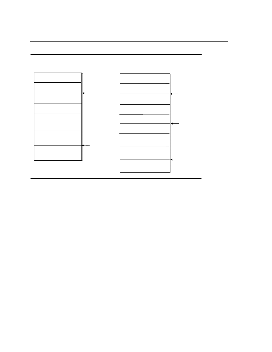
Stack Alignment for Streaming SIMD Extensions
E
E-3
As an optimization, an alternate entry point can be created that can be called
when proper stack alignment is provided by the caller. Using call graph
profiling of the VTune™ analyzer, calls to the normal (unaligned) entry
point can be optimized into calls to the (alternate) aligned entry point when
the stack can be proven to be properly aligned. Furthermore, a function
alignment requirement attribute can be modified throughout the call graph
so as to cause the least number of calls to unaligned entry points. As an
example of this, suppose function F has only a stack alignment requirement
of 4, but it calls function G at many call sites, and in a loop. If G’s alignment
requirement is 16, then by promoting F’s alignment requirement to 16, and
making all calls to G go to its aligned entry point, the compiler can
minimize the number of times that control passes through the unaligned
Figure E-1
Stack Frames Based on Alignment Type
Parameter
Pointer
EBP
ESP
EBP-based Aligned Frame
Parameters
Return Address
Padding
Previous EBP
Local Variables and
Spill Slots
Parameter Passing
Space
EBP-frame Saved
Register Area
Return Address 1
SEH/CEH Record
Parameter
Pointer
ESP
ESP-based Aligned Frame
Parameters
Return Address
Padding
Register Save Area
Local Variables and
Spill Slots
__cdecl Parameter
Passing Space
__stdcall Parameter
Passing Space

E-4
E
Intel Architecture Optimization Reference Manual
entry points. Example E-1 and Example E-2 in the following sections
illustrate this technique. Note the entry points
foo
and
foo.aligned
, the
latter is the alternate aligned entry point.
Aligned
esp
-Based Stack Frames
This section discusses data and parameter alignment and the
declspec(align)
extended attribute, which can be used to request
alignment in C and C++ code. In creating
esp
-based stack frames, the
compiler adds padding between the return address and the register save area
as shown in Example 3-9. This frame can be used only when debug
information is not requested, there is no need for exception handling
support, inlined assembly is not used, and there are no calls to
alloca
within the function.
If the above conditions are not met, an aligned
ebp
-based frame must be
used. When using this type of frame, the sum of the sizes of the return
address, saved registers, local variables, register spill slots, and parameter
space must be a multiple of 16 bytes. This causes the base of the parameter
space to be 16-byte aligned. In addition, any space reserved for passing
parameters for
stdcall
functions also must be a multiple of 16 bytes. This
means that the caller needs to clean up some of the stack space when the
size of the parameters pushed for a call to a
stdcall
function is not a
multiple of 16. If the caller does not do this, the stack pointer is not restored
to its pre-call value.
In Example E-1, we have 12 bytes on the stack after the point of alignment
from the caller: the return pointer,
ebx
and
edx
. Thus, we need to add four
more to the stack pointer to achieve alignment. Assuming 16 bytes of stack
space are needed for local variables, the compiler adds 16 + 4 = 20 bytes to
esp
, making
esp
aligned to a 0 mod 16 address.

Stack Alignment for Streaming SIMD Extensions
E
E-5
Example E-1 Aligned esp-Based Stack Frames
void _cdecl foo (int k)
{
int j;
foo: // See Note A
push ebx
mov ebx, esp
sub esp, 0x00000008
and esp, 0xfffffff0
add esp, 0x00000008
jmp common
foo.aligned:
push ebx
mov ebx, esp
common: // See Note B
push edx
sub esp, 20
j = k;
mov edx, [ebx + 8]
mov [esp + 16], edx
foo(5);
mov [esp], 5
call foo.aligned
return j;
mov eax, [esp + 16]
add esp, 20
pop edx
mov esp, ebx
pop ebx
ret
_________________________________________________________________________

E-6
E
Intel Architecture Optimization Reference Manual
Aligned
ebp
-Based Stack Frames
In
ebp
-based frames, padding is also inserted immediately before the return
address. However, this frame is slightly unusual in that the return address
may actually reside in two different places in the stack. This occurs
whenever padding must be added and exception handling is in effect for the
function. Example E-2 shows the code generated for this type of frame. The
stack location of the return address is aligned 12 mod 16. This means that
the value of
ebp
always satisfies the condition
(ebp & 0x0f) == 0x08
.
In this case, the sum of the sizes of the return address, the previous
ebp
, the
exception handling record, the local variables, and the spill area must be a
multiple of 16 bytes. In addition, the parameter passing space must be a
multiple of 16 bytes. For a call to a
stdcall
function, it is necessary for the
caller to reserve some stack space if the size of the parameter block being
pushed is not a multiple of 16.
Example E-2 Aligned ebp-based Stack Frames
void _stdcall foo (int k)
{
int j;
foo:
push ebx
mov ebx, esp
sub esp, 0x00000008
and esp, 0xfffffff0
_____________________________________________________________
continued
NOTE.
A. Aligned entry points assume that parameter block beginnings
are aligned. This places the stack pointer at a 12 mod 16 boundary, as
the return pointer has been pushed. Thus, the unaligned entry point must
force the stack pointer to this boundary.
B. The code at the common label assumes the stack is at an 8 mod
16 boundary, and adds sufficient space to the stack so that the stack
pointer is aligned to a 0 mod 16 boundary.

Stack Alignment for Streaming SIMD Extensions
E
E-7
Example E-2 Aligned ebp-based Stack Frames (continued)
add esp, 0x00000008 // esp is (8 mod 16)
// after add
jmp common
foo.aligned:
push ebx // esp is (8 mod 16)
// after push
mov ebx, esp
common:
push ebp // this slot will be
// used for duplicate
// return pt
push ebp // esp is (0 mod 16)
// after push
// (rtn,ebx,ebp,ebp)
mov ebp, [ebx + 4] // fetch return pointer
and store
mov [esp + 4], ebp // relative to ebp
// (rtn,ebx,rtn,ebp)
mov ebp, esp // ebp is (0 mod 16)
sub esp, 28 // esp is (4 mod 16)
// see Note A
push edx // esp is (0 mod 16)
// after push
// the goal is to make
// esp and ebp (0 mod
// 16) here
j = k;
mov edx, [ebx + 8] // k is (0 mod 16) if
// caller aligned
// his stack
mov [ebp - 16], edx // J is (0 mod 16)
foo(5);
add esp,-4 // normal call sequence
// to unaligned entry
mov [esp],5
_____________________________________________________________
continued

E-8
E
Intel Architecture Optimization Reference Manual
Example E-2 Aligned ebp-based Stack Frames (continued)
call foo // for stdcall, callee
// cleans up stack
foo.aligned(5);
add esp,-16 // aligned entry, this
// should be a
// multiple of 16
mov [esp],5
call foo.aligned
add esp,12 // see Note B
return j;
mov eax,[ebp-16]
pop edx
mov esp,ebp
pop ebp
mov esp,ebx
pop ebx
ret 4
}
_____________________________________________________________
NOTE.
A. Here we allow for local variables. However, this value should
be adjusted so that, after pushing the saved registers, esp is 0 mod 16.
B. Just prior to the call, esp is 0 mod 16. To maintain alignment,
esp should be adjusted by 16. When a callee uses the stdcall calling
sequence, the stack pointer is restored by the callee. The final addition of
12 compensates for the fact that only 4 bytes were passed, rather than 16,
and thus the caller must account for the remaining adjustment.

Stack Alignment for Streaming SIMD Extensions
E
E-9
Stack Frame Optimizations
The Intel C/C++ Compiler provides certain optimizations that may improve
the way aligned frames are set up and used. These optimizations are as
follows:
•
If a procedure is defined to leave the stack frame 16-byte-aligned and it
calls another procedure that requires 16-byte alignment, then the
callee’s aligned entry point is called, bypassing all of the unnecessary
aligning code.
•
If a static function requires 16-byte alignment, and it can be proven to
be called only by other functions that require 16-byte alignment, then
that function will not have any alignment code in it. That is, the
compiler will not use
ebx
to point to the argument block and it will not
have alternate entry points, because this function will never be entered
with an unaligned frame.
Inlined Assembly and
ebx
When using aligned frames, the
ebx
register generally should not be
modified in inlined assembly blocks since
ebx
is used to keep track of the
argument block. Programmers may modify
ebx
only if they do not need to
access the arguments and provided they save
ebx
and restore it before the
end of the function (since
esp
is restored relative to
ebx
in the function’s
epilog).
For additional information on the use of
ebx
in inline assembly code and
other related issues, see the Intel application note AP-833, Data Alignment
and Programming Issues with the Intel C/C++ Compiler, order number
243872, and AP-589, Software Conventions for the Streaming SIMD
Extensions, order number 243873.
CAUTION.
Do not use the
ebx
register in inline assembly functions
that use dynamic stack alignment for double, __m64, and __m128 local
variables unless you save and restore
ebx
each time you use it. The Intel
C/C++ Compiler uses the
ebx
register to control alignment of variables
of these types, so the use of
ebx
, without preserving it, will cause
unexpected program execution.


F-1
The Mathematics
of Prefetch Scheduling
Distance
F
This appendix discusses how far away to insert prefetch instructions. It
presents a mathematical model allowing you to deduce a simplified
equation which you can use for determining the prefetch scheduling
distance (PSD) for your application.
For your convenience, the first section presents this simplified equation; the
second section provides the background for this equation: the mathematical
model of the calculation.
Simplified Equation
A simplified equation to compute PSD is as follows:
where
psd
is prefetch scheduling distance.
Nlookup
is the number of clocks for lookup latency. This
parameter is system-dependent. The type of memory
used and the chipset implementation affect its value.
Nxfer
is the number of clocks to transfer a cache-line. This
parameter is implementation-dependent.
N
pref
and
N
st
are the numbers of cache lines to be prefetched and
stored.
psd
Nlookup
Nxfer
N
pref
N
st
+
(
)
⋅
+
CPI N
inst
⋅
-------------------------------------------------------------------------------
=

F-2
F
Intel Architecture Optimization Reference Manual
CPI
is the number of clocks per instruction. This parameter
is implementation-dependent.
N
inst
is the number of instructions in the scope of one loop
iteration.
Consider the following example of a heuristic equation assuming that
parameters have the values as indicated:
where 60 corresponds to
Nlookup
, 25 to
Nxfer
, and 1.5 to
CPI
.
The values of the parameters in the equation can be derived from the
documentation for memory components and chipsets as well as from vendor
datasheets.
Mathematical Model for PSD
The parameters used in the mathematics discussed are as follows:
psd
prefetch scheduling distance (measured in number of
iterations)
il
iteration latency
T
c
computation latency per iteration with prefetch caches
T
l
memory leadoff latency including cache miss latency,
chip set latency, bus arbitration, etc.
CAUTION.
The values in this example are for illustration only and do
not represent the actual values for these parameters. The example is
provided as a “starting point approximation” of calculating the prefetch
scheduling distance using the above formula. Experimenting with the
instruction around the “starting point approximation” may be required
to achieve the best possible performance
.
psd
60
25
N
pref
N
st
+
(
)
⋅
+
1.5 N
inst
⋅
-----------------------------------------------------
=

The Mathematics of Prefetch Scheduling Distance
F
F-3
T
b
data transfer latency which is equal to number of lines
per iteration * line burst latency
Note that the potential effects of µop reordering are not factored into the
estimations discussed.
Examine Example F-1 that uses the
prefetchnta
instruction with a
prefetch scheduling distance of 3, that is, psd = 3. The data prefetched in
iteration i, will actually be used in iteration i+3. T
c
represents the cycles
needed to execute
top_loop
- assuming all the memory accesses hit L1
while il (iteration latency) represents the cycles needed to execute this loop
with actually run-time memory footprint. T
c
can be determined by
computing the critical path latency of the code dependency graph. This
work is quite arduous without help from special performance
characterization tools or compilers. A simple heuristic for estimating the T
c
value is to count the number of instructions in the critical path and multiply
the number with an artificial CPI. A reasonable CPI value would be
somewhere between 1.0 and 1.5 depending on the quality of code
scheduling.
Example F-1 Calculating Insertion for Scheduling Distance of 3
top_loop:
prefetchnta [edx+esi+32*3]
prefetchnta [edx*4+esi+32*3]
. . . . .
movaps xmm1, [edx+esi]
movaps xmm2, [edx*4+esi]
movaps xmm3, [edx+esi+16]
movaps xmm4, [edx*4+esi+16]
. . . . .
. . .
add esi, 32
cmp esi, ecx
jl top_loop
______________________________________________________
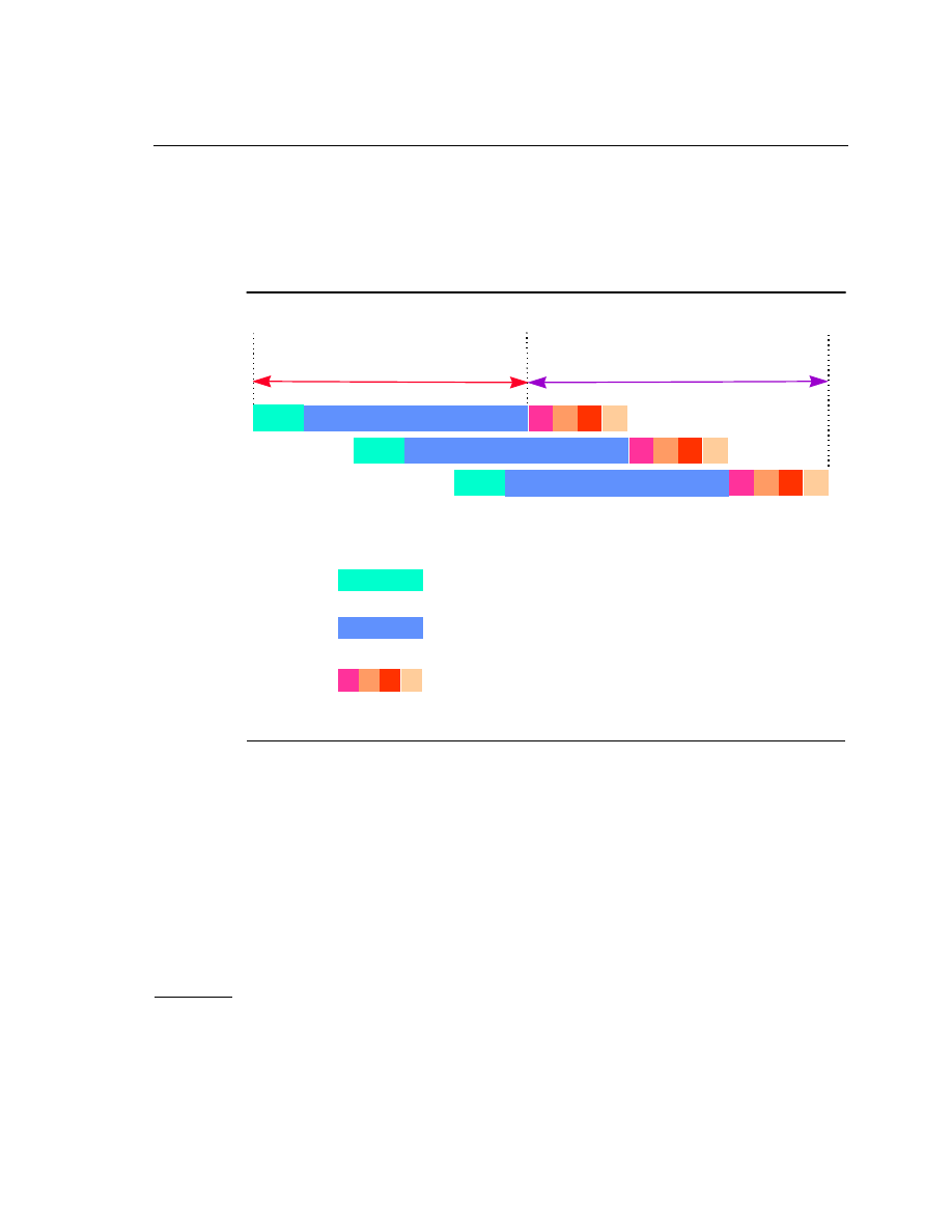
F-4
F
Intel Architecture Optimization Reference Manual
Memory access plays a pivotal role in prefetch scheduling. For more
understanding of a memory subsystem, consider a Streaming SIMD
Extensions memory pipeline depicted in Figure F-1.
Assume that three cache lines are accessed per iteration and four chunks of
data are returned per iteration for each cache line. Also assume these 3
accesses are pipelined in memory subsystem. Based on these assumptions,
T
b
= 3 * 4 = 12 FSB cycles.
Figure F-1
Pentium
®
II
and Pentium III Processors Memory Pipeline Sketch
1 2 3 4
1
1 2 3 4
1
1 2 3 4
1
T
l
T
b
:
L2 lookup miss latency
:
Memory page access leadoff latency
:
Latency for 4 chunks returned per line
2 3
1
4
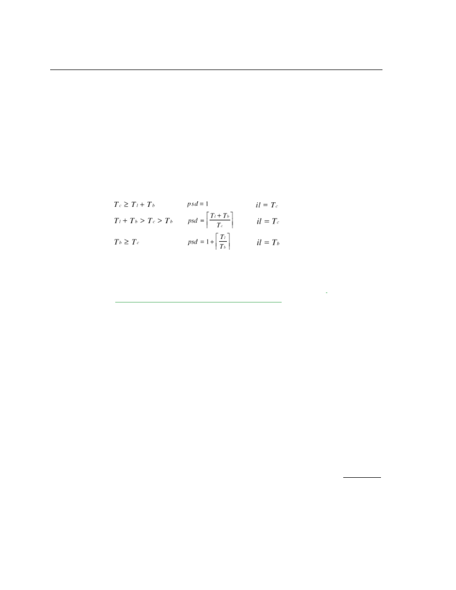
The Mathematics of Prefetch Scheduling Distance
F
F-5
T
l
varies dynamically and is also system hardware-dependent. The static
variants include the core-to-front-side-bus ratio, memory manufacturer and
memory controller (chipset). The dynamic variants include the memory
page open/miss occasions, memory accesses sequence, different memory
types, and so on.
To determine the proper prefetch scheduling distance, follow these steps
and formulae:
•
Optimize T
c
as much as possible
•
Use the following set of formulae to calculate the proper prefetch
scheduling distance:
•
Schedule the prefetch instructions according to the computed prefetch
scheduling distance.
•
For optimized memory performance, apply techniques described in
“Memory Optimization Using Prefetch” in Chapter 6
.
The following sections explain and illustrate the architectural considerations
involved in the prefetch scheduling distance formulae above.
No Preloading or Prefetch
The traditional programming approach does not perform data preloading or
prefetch. It is sequential in nature and will experience stalls because the
memory is unable to provide the data immediately when the execution
pipeline requires it. Examine Figure F-2.
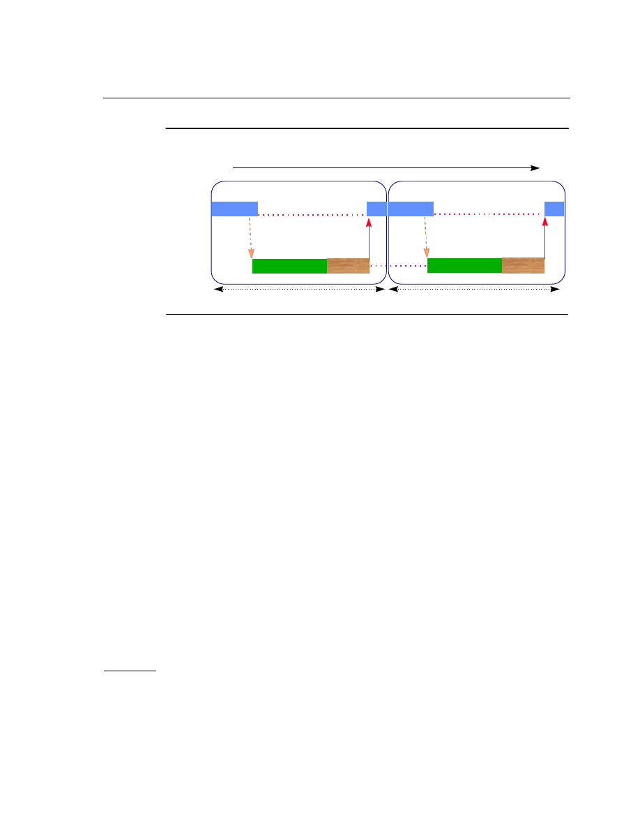
F-6
F
Intel Architecture Optimization Reference Manual
As you can see from Figure F-2, the execution pipeline is stalled while
waiting for data to be returned from memory. On the other hand, the front
side bus is idle during the computation portion of the loop. The memory
access latencies could be hidden behind execution if data could be fetched
earlier during the bus idle time.
Further analyzing Figure 6-10,
•
assume execution cannot continue till last chunk returned and
•
δ
f
indicates flow data dependency that stalls the execution pipelines
With these two things in mind the iteration latency (il) is computed as
follows:
The iteration latency is approximately equal to the computation latency plus
the memory leadoff latency (includes cache miss latency, chipset latency,
bus arbitration, and so on.) plus the data transfer latency where
transfer latency= number of lines per iteration * line burst latency.
Figure F-2
Execution Pipeline, No Preloading or Prefetch
Execution cycles
Execution
pipeline
(i+1)
th
iteration
T
l
T
b
δ
f
T
c
-
T
∆
T
∆
T
l
T
b
δ
f
T
∆
T
c
-
T
∆
Front-Side
Bus
i
th
iteration
issue loads
issue loads
Execution units idle
Execution units idle
FSB idle
il
T
c
T
+
l
T
b
+
≅
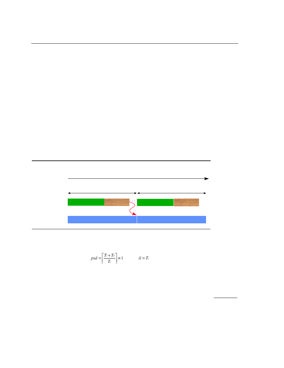
The Mathematics of Prefetch Scheduling Distance
F
F-7
This means that the decoupled memory and execution are ineffective to
explore the parallelism because of flow dependency. That is the case where
prefetch can be useful by removing the bubbles in either the execution
pipeline or the memory pipeline.
With an ideal placement of the data prefetching, the iteration latency should
be either bound by execution latency or memory latency, that is
il = maximum(T
c
, T
b
).
Compute Bound (Case:Tc >= T
l
+ T
b
)
Figure F-3 represents the case when the compute latency is greater than or
equal to the memory leadoff latency plus the data transfer latency. In this
case, the prefetch scheduling distance is exactly 1, i.e. prefetch data one
iteration ahead is good enough. The data for loop iteration i can be
prefetched during loop iteration i-1, the
δ
f
symbol between front-side bus
and execution pipeline indicates the data flow dependency.
The following formula shows the relationship among the parameters:
Figure F-3
Compute Bound Execution Pipeline
Front-Side Bus
Execution pipeline
T
c
T
l
T
b
Iteration i
Iteration i+1
T
c
T
l
T
b
Execution cycles
δ
f
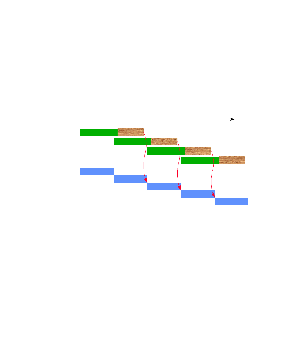
F-8
F
Intel Architecture Optimization Reference Manual
It can be seen from this relationship that the iteration latency is equal to the
computation latency, which means the memory accesses are executed in
background and their latencies are completely hidden.
Compute Bound (Case: T
l
+ T
b
> T
c
> T
b
)
Now consider the next case by first examining Figure F-4.
For this particular example the prefetch scheduling distance is greater than
1. Data being prefetched for iteration i will be consumed in iteration i+2.
Figure 6-12 represents the case when the leadoff latency plus data transfer
latency is greater than the compute latency, which is greater than the data
transfer latency. The following relationship can be used to compute the
prefetch scheduling distance.
Figure F-4
Compute Bound Execution Pipeline
Execution cycles
Front-Side Bus
Execution pipeline
i
i+1
i+2
i+3
i
i+1
i+2
i+3
T
c
T
c
T
c
T
c
T
l
T
b
T
l
T
b
T
l
T
b
T
l
T
b
δ
f
δ
f
T
c
δ
f
i+4
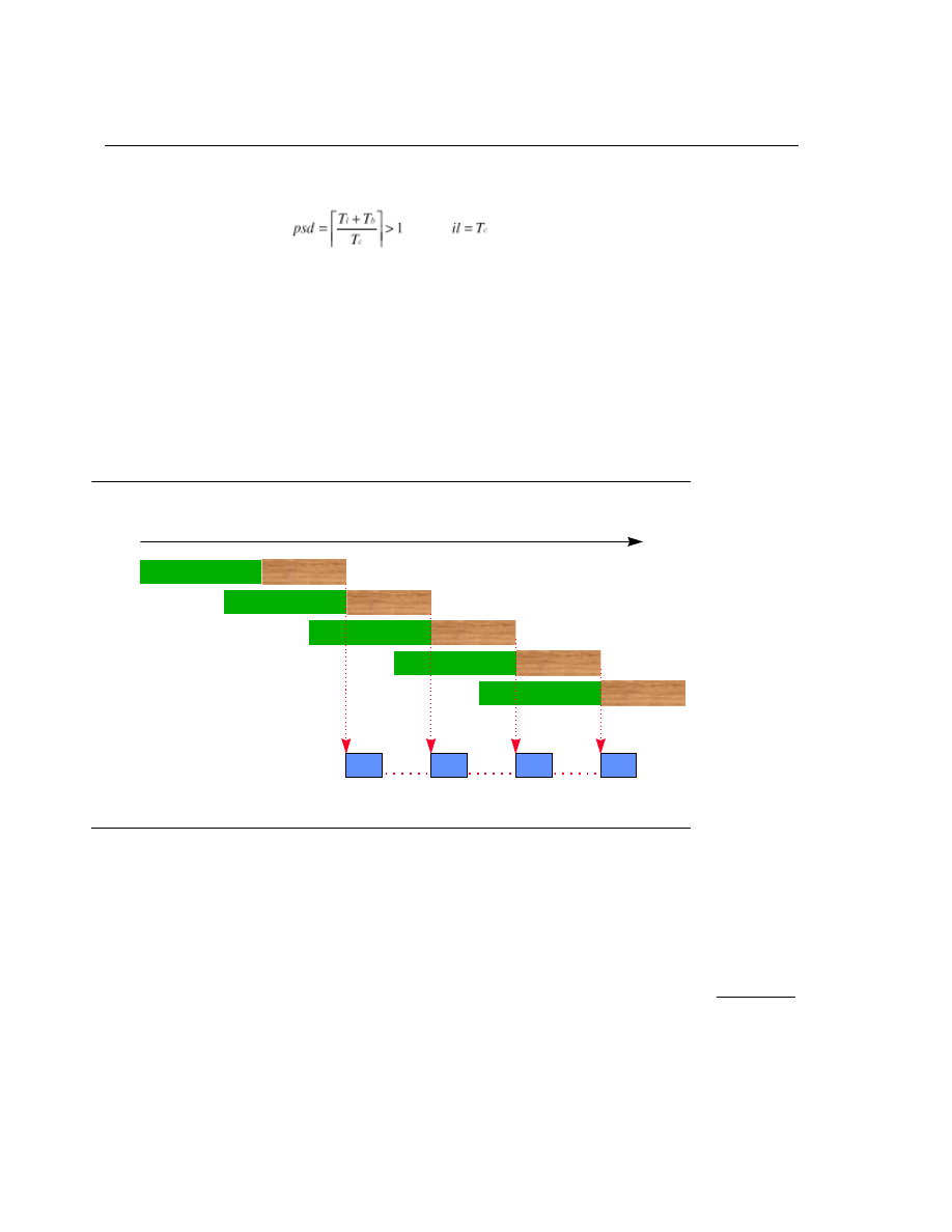
The Mathematics of Prefetch Scheduling Distance
F
F-9
In consequence, the iteration latency is also equal to the computation
latency, that is, compute bound program.
Memory Throughput Bound (Case: T
b
>= T
c
)
When the application or loop is memory throughput bound, the memory
latency is no way to be hidden. Under such circumstances, the burst latency
is always greater than the compute latency. Examine Figure F-5.
The following relationship calculates the prefetch scheduling distance (or
prefetch iteration distance) for the case when memory throughput latency is
greater than the compute latency.
Figure F-5
Memory Throughput Bound Pipeline
i
Execution cycles
Execution pipeline
i+pid
T
c
δ
f
T
c
T
c
T
c
i+pid+1
i+pid+2
i+pid+3
Front-Side Bus
T
l
T
b
T
l
T
b
T
l
T
b
T
l
T
b
T
l
T
b
δ
f
δ
f
δ
f
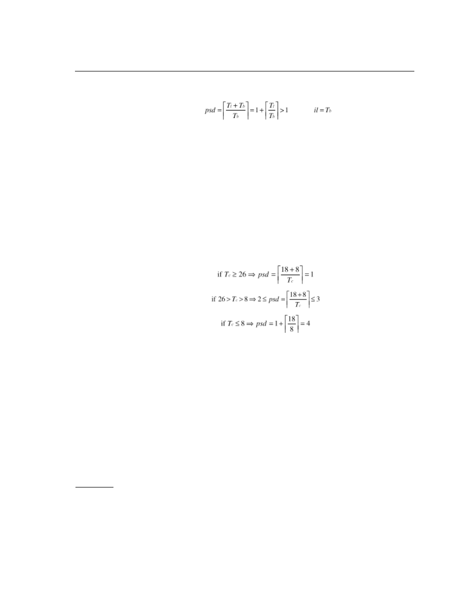
F-10
F
Intel Architecture Optimization Reference Manual
Apparently, the iteration latency is dominant by the memory throughput and
you cannot do much about it. Typically, data copy from one space to another
space, for example, graphics driver moving data from writeback memory to
you cannot do much about it. Typically, data copy from one space to another
space, for example, graphics driver moving data from writeback memory to
write-combining memory, belongs to this category, where performance
advantage from prefetch instructions will be marginal.
Example
As an example of the previous cases consider the following conditions for
computation latency and the memory throughput latencies. Assume T
l
= 18
and T
b
= 8 (in front side bus cycles).
Now for the case T
l
=18, T
b
=8 (2 cache lines are needed per iteration)
examine the following graph. Consider the graph of accesses per iteration in
example 1, Figure F-6.
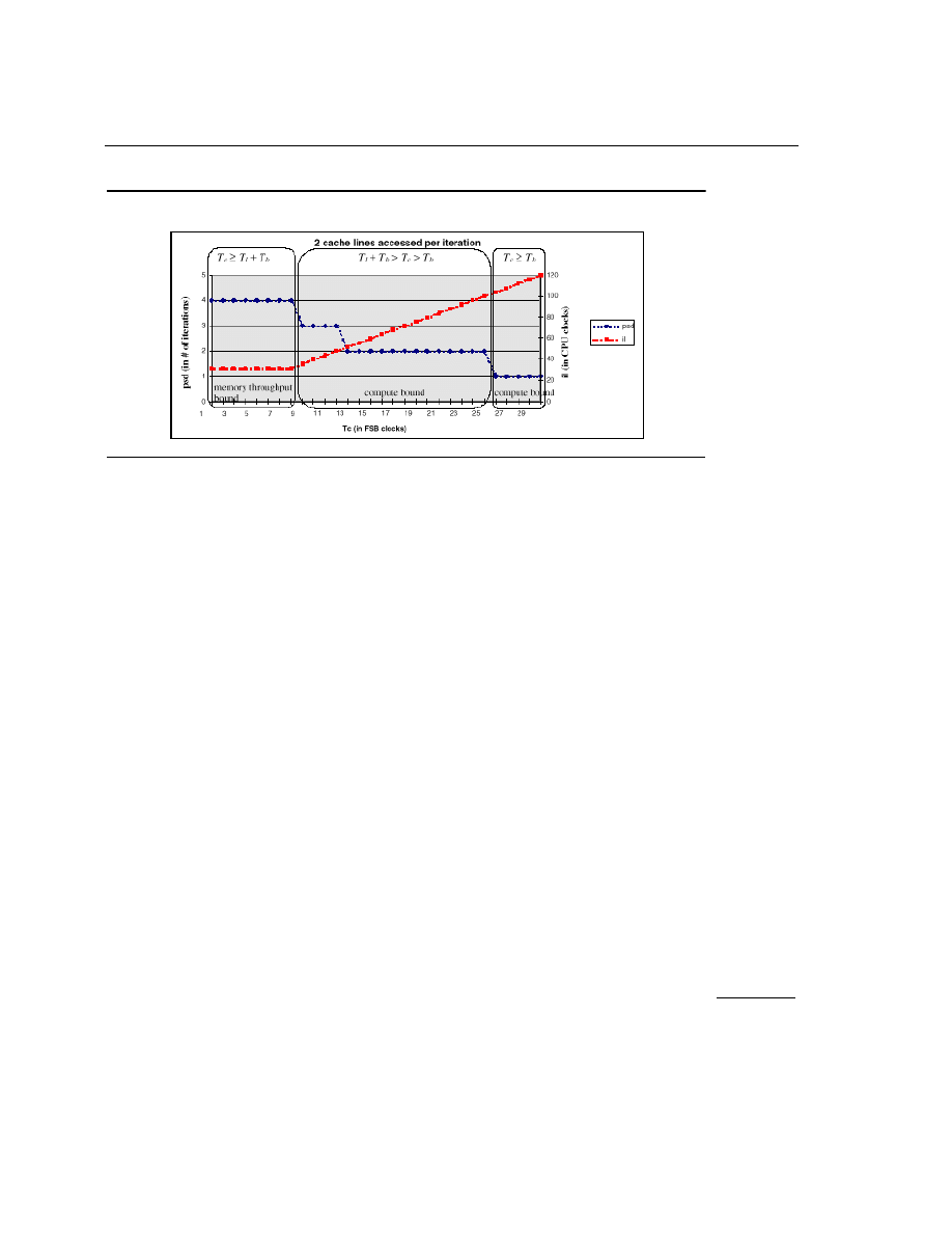
The Mathematics of Prefetch Scheduling Distance
F
F-11
The prefetch scheduling distance is a step function of T
c
, the computation
latency. The steady state iteration latency (il) is either memory-bound or
compute-bound depending on T
c
if prefetches are scheduled effectively.
The graph in example 2 of accesses per iteration in Figure F-7 shows the
results for prefetching multiple cache lines per iteration. The cases shown
are for 2, 4, and 6 cache lines per iteration, resulting in differing burst
latencies. (T
l
=18, T
b
=8, 16, 24).
Figure F-6
Accesses per Iteration, Example 1
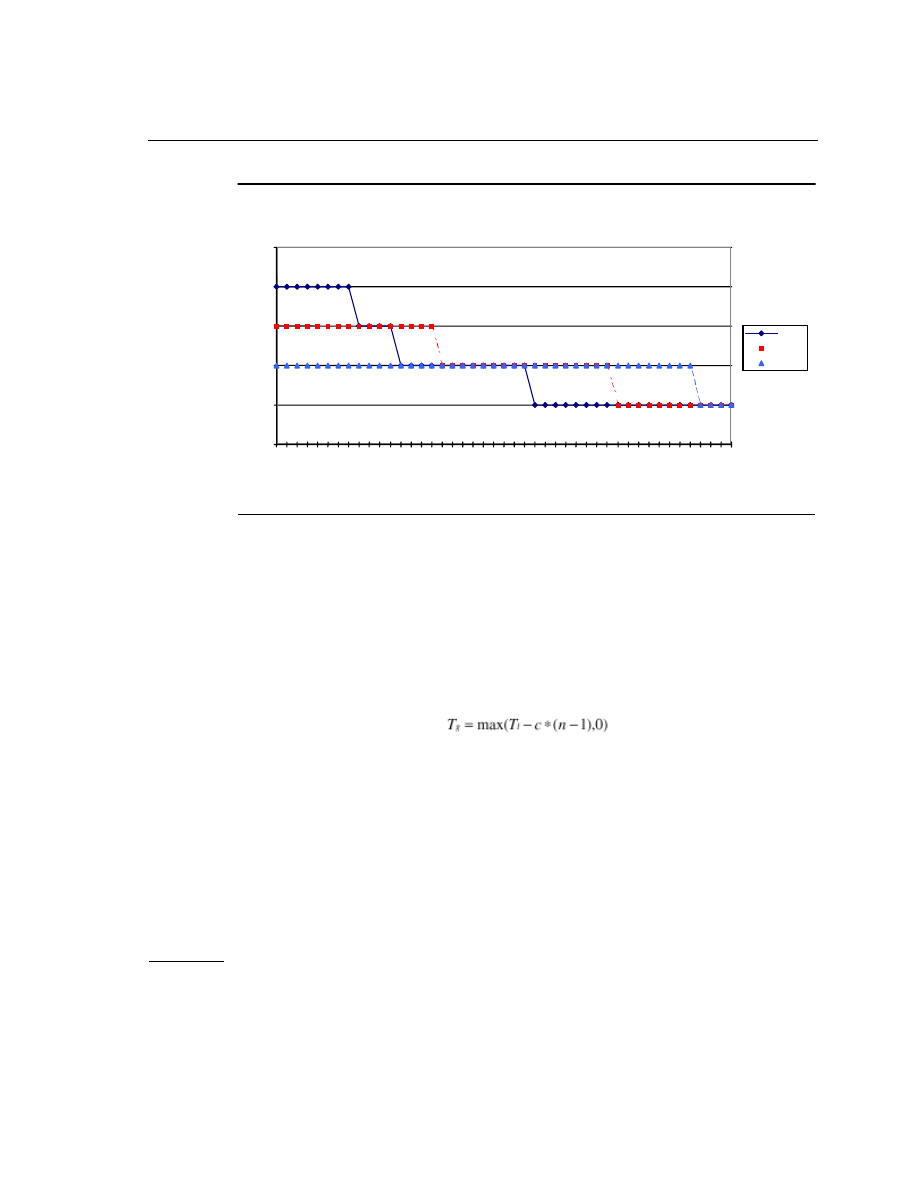
F-12
F
Intel Architecture Optimization Reference Manual
In reality, the front-side bus (FSB) pipelining depth is limited, that is, only
four transactions are allowed at a time in the Pentium
®
III
processor. Hence
a transaction bubble or gap, T
g
, (gap due to idle bus of imperfect front side
bus pipelining) will be observed on FSB activities. This leads to
consideration of the transaction gap in computing the prefetch scheduling
distance. The transaction gap, T
g
, must be factored into the burst cycles, T
b
,
for the calculation of prefetch scheduling distance.
The following relationship shows computation of the transaction gap.
where T
l
is the memory leadoff latency, c is the number of chunks per cache
line and n is the FSB pipelining depth.
Figure F-7
Accesses per Iteration, Example 2
0
1
2
3
4
5
1
3
5
7
9
11
13
15
17
19
21
23
25
27
29
31
33
35
37
39
41
43
45
Tc (in FSB clocks)
ps
d
2 lines
4 lines
6 lines
psd for different number of cache lines prefetched per iteration

Index-1
Index
3D transformation algorithms, A-7
A
of signed numbers, 4-15
of unsigned numbers, 4-14
accesses per iteration, F-11, F-12
aligned ebp-based frame, E-4, E-6
aligned esp-based stack frames, E-4
coe, 2-11
data, 2-12
rules, 2-11
application performance tools, 7-1
assembly coach techniques, 7-13
assembly code for SoA transformation, A-13
automatic masked exception handling, 5-38
automatic processor dispatch support, 7-15
automatic vectorization, 3-13, 3-14
B
branch misprediction ratio, 2-8
Branch Prediction, 1-5, 2-1, 2-2
C
cache blocking techniques, 6-18
cache management
simple memory copy, 6-28
video decoder, 6-27
video encoder, 6-27
cacheability control instructions, 6-9

Index
Index-2
changing the rounding mode, 2-26
checking for MMX technology support, 3-2
checking for Streaming SIMD Extensions
clipping to an arbitrary signed range, 4-17
clipping to an arbitrary unsigned range, 4-19
code optimization advice, 7-11, 7-13
code optimization options, 7-14
absolute difference of signed numbers, 4-15
absolute difference of unsigned numbers,
absolute value, 4-17
clipping to an arbitrary signed range, 4-17
clipping to an arbitrary unsigned range, 4-19
generating constants, 4-20
interleaved pack with saturation, 4-9
interleaved pack without saturation, 4-11
non-interleaved unpack, 4-12
signed unpack, 4-8
simplified clipping to an arbitrary signed
comparing register values, 2-19
compiler intrinsics
_mm_load, 6-26
_mm_prefetch, 6-26
_mm_stream, 6-26
compiler-supported alignment, 3-18
complex FIR filter algorithm
reducing non-value-added instructions, A-21
unrolling the loop, A-21
using a SIMD data structure, A-21
complex instructions, 1-4, 2-17
computation-intensive code, 3-7
conditional branches, 1-7, 2-5
conditional moves emulation, 5-31
converting code to MMX technology, 3-4
D

Intel Architecture Optimization Reference Manual
Index-3
dynamic assembly analysis, 7-10
dynamic branch prediction, 2-2, 2-3
E
eliminating branches, 2-5, 2-7, 2-8
eliminating unnecessary micro-ops, A-20
EMMS instruction, 4-3, 4-5, 4-6, 5-4
executing instructions out-of-order, 5-28
extract word instruction, 4-22
F
unrolling the loop, A-19
wrapping the loop around, A-18
floating-point applications, 2-20
floating-point arithmetic precision options, 7-17
floating-point code
improving parallelism, 2-21
loop unrolling, 2-28
memory access stall information, 2-24
operations with integer operands, 2-30
optimizing, 2-21
transcendental functions, 2-31
floating-point execution unit, 1-9
floating-point operations with integer operands,
forwarding from stores to loads, 5-31
G
general optimization techniques, 2-1
branch prediction, 2-2
dynamic branch prediction, 2-2
eliminate branches, 2-6
eliminating branches, 2-5
static prediction, 2-3
H
hiding one-clock latency, 2-29
I
incorporating prefetch into code, 6-23

Index
Index-4
inline expansion of library functions option, 7-17
integer and floating-point multiply, 2-30
integer-intensive application, 4-1, 4-2
Intel Performance Library Suite, 7-1
interaction with x87 numeric exceptions, 5-41
interleaved pack with saturation, 4-9
interleaved pack without saturation, 4-11
interprocedural optimization, 7-17
IPO. See interprocedural optimization
L
loading and storing to and from the same DRAM
loop unrolling. See unrolling the loop.
M
memory access stall information, 2-24
memory O=optimization U=using P=prefetch,
memory optimizations
loading and storing to and from the same
partial memory accesses, 4-28
using aligned stores, 4-33
memory reference instructions, 2-19
minimize cache pollution on write, A-20
minimizing cache pollution, 6-5
minimizing pointer arithmetic, A-20
minimizing prefetches number, 6-15
misaligned accesses event, 2-13
misalignment in the FIR filter, 3-16
mixing MMX technology code and
mixing SIMD-integer and SIMD-fp instructions,
motion estimation algorithm, A-14
motion-error calculation, A-15

Intel Architecture Optimization Reference Manual
Index-5
N
new SIMD-integer instructions, 4-21
extract word, 4-22
insert word, 4-22
move byte mask to integer, 4-24
packed average byte or word), 4-27
packed multiply high unsigned, 4-25
packed shuffle word, 4-25
packed signed integer word maximum, 4-23
packed signed integer word minimum, 4-23
packed sum of absolute differences, 4-26
packed unsigned integer byte maximum,
packed unsigned integer byte minimum, 4-24
Newton-Raphson
approximation, A-9
formula, A-2
iterations, 5-2, A-2
Newton-Raphson method, A-2, A-3
non-temporal store instructions, 6-5
O
optimization of upsampling algorithm, A-16
3D Transformation, A-7
FIR filter, A-17
motion estimation, A-14
Newton-Raphson method with the reciprocal
optimizing cache utilization
optimizing floating-point applications
benefits from SIMD-fp instructions, 5-3
conditional moves, 5-31
copying, shuffling, 5-17
CPUID usage, 5-5
data alignment, 5-5
data arrangement, 5-6
data deswizzling, 5-13
data swizzling, 5-10
data swizzling using intrinsics, 5-11
EMMS instruction, 5-4
horizontal ADD, 5-18
modulo scheduling, 5-25
overlapping iterations, 5-27
planning considerations, 5-2
port balancing, 5-33
rules and suggestions, 5-1
scalar code, 5-3
schedule with the triple/quadruple rule, 5-24
scheduling avoid RAT stalls, 5-31
scheduling instructions, 5-22
scheduling instructions out-of-order, 5-28
vertical versus horizontal computation, 5-6
optimizing floating-point code, 2-21
P

Index
Index-6
packed average byte or word), 4-27
packed multiply high unsigned, 4-25
packed signed integer word maximum, 4-23
packed signed integer word minimum, 4-23
packed sum of absolute differences, 4-26
packed unsigned integer byte maximum, 4-23
packed unsigned integer byte minimum, 4-24
parallel multiplications, A-17
partial register stalls, 2-1, 2-8
performance counter events, 7-4
Performance Library Suite, 7-18
performance-monitoring counters, B-1
performance-monitoring events, B-2
PGO. See profile-guided optimization
PLS. See Performance Library Suite
predictable memory access patterns, 6-4
prefetch and cacheability Instructions, 6-2
prefetch and loadiInstructions, 6-4
prefetch concatenation, 6-13, 6-14
prefetch instruction, 6-1, A-8, A-15
prefetch instruction considerations, 6-12
prefetch scheduling distance, 6-12, F-5, F-7, F-9
prefetch use
flow dependency, 6-4
predictable memory access patterns, 6-4
time-consuming innermost loops, 6-4
profile-guided optimization, 7-18
R

Intel Architecture Optimization Reference Manual
Index-7
reducing data dependency, A-17
reducing non-value-added instructions, A-21
reducing register pressure, A-17
register viewing tool, 7-2, 7-21
RVT. See register viewing tool
S
event-based, 7-4
time-based, 7-3
scheduling for the reorder buffer, A-18
scheduling for the reservation station, A-18
scheduling to avoid RAT stalls, 5-31
scheduling with the triple-quadruple rule, 5-24
separating memory accesses from operations,
SIMD instruction port assignments, 4-7
SIMD. See single-instruction, multiple data.
simplified 3D geometry pipeline, 6-10
simplified clipping to an arbitrary signed range,
single-instruction, multiple-data, 3-1
single-pass versus multi-pass execution, 6-23
smoothed upsample algorithm, A-15
SoA. See straucture of arrays.
software write-combining, 6-25
static assembly analyzer, 7-10
static branch prediction algorithm, 2-4
static prediction algorithm, 2-3
streaming non-temporal stores, 6-6
streaming stores, 6-28
approach A, 6-7
approach B, 6-7
coherent requests, 6-8
non-coherent requests, 6-8
strip-mining, 3-23, 3-25, 6-21, 6-22
sum of absolute differences, A-15
swizzling data. See data swizzling.
T
targeting a processor option, 7-15
time-consuming innermost loops, 6-4
TLB. See transaction lookaside buffer
transaction lookaside buffer, 6-28

Index
Index-8
U
unrolling the loop, A-19, A-21
using MMX code for copy or shuffling functions,
vectorizer switch options, 7-16
vertical versus horizontal computation, 5-6
VTune analyzer, 2-10, 3-6, 7-1
VTune Performance Analyzer, 3-6
W
Document Outline
- Intel® Architecture Optimization Reference Manual
- Revision History
- Disclaimer
- Contents
- Introduction
- 1 Processor Architecture Overview
- 2 General Optimization Guidelines
- Integer Coding Guidelines
- Branch Prediction
- Partial Register Stalls
- Alignment Rules and Guidelines
- Instruction Scheduling
- Instruction Selection
- Improving the Performance of Floating-point Applications
- 3 Coding for SIMD Architectures
- 4 Using SIMD Integer Instructions
- General Rules on SIMD Integer Code
- Planning Considerations
- CPUID Usage for Detection of Pentium® III Processor SIMD Integer Instructions
- Using SIMD Integer, Floating-Point, and MMX™ Technology Instructions
- Data Alignment
- SIMD Integer and SIMD Floating-point Instructions
- Coding Techniques for MMX Technology SIMD Integer Instructions
- Unsigned Unpack
- Signed Unpack
- Interleaved Pack without Saturation
- Non-Interleaved Unpack
- Complex Multiply by a Constant
- Absolute Difference of Unsigned Numbers
- Absolute Difference of Signed Numbers
- Absolute Value
- Clipping to an Arbitrary Signed Range [high, low]
- Clipping to an Arbitrary Unsigned Range [high, low]
- Generating Constants
- Coding Techniques for Integer Streaming SIMD Extensions
- Extract Word
- Insert Word
- Packed Signed Integer Word Maximum
- Packed Unsigned Integer Byte Maximum
- Packed Signed Integer Word Minimum
- Packed Unsigned Integer Byte Minimum
- Move Byte Mask to Integer
- Packed Multiply High Unsigned
- Packed Shuffle Word
- Packed Sum of Absolute Differences
- Packed Average (Byte/Word)
- Memory Optimizations
- Partial Memory Accesses
- Instruction Selection to Reduce Memory Access Hits
- Increasing Bandwidth of Memory Fills and Video Fills
- Increasing Memory Bandwidth Using the MOVQ Instruction
- Increasing Memory Bandwidth by Loading and Storing to and from the Same DRAM Page
- Increasing the Memory Fill Bandwidth by Using Aligned Stores
- Use 64-Bit Stores to Increase the Bandwidth to Video
- Increase the Bandwidth to Video Using Aligned Stores
- Scheduling for the SIMD Integer Instructions
- 5 Optimizing Floating-point Applications
- Rules and Suggestions
- Planning Considerations
- Which Part of the Code Benefits from SIMD Floating-point Instructions?
- MMX Technology and Streaming SIMD Extensions Floating-point Code
- Scalar Code Optimization
- EMMS Instruction Usage Guidelines
- CPUID Usage for Detection of SIMD Floating-point Support
- Data Alignment
- Data Arrangement
- Scheduling
- Scheduling with the Triple-Quadruple Rule
- Modulo Scheduling (or Software Pipelining)
- Scheduling to Avoid Register Allocation Stalls
- Forwarding from Stores to Loads
- Conditional Moves and Port Balancing
- Streaming SIMD Extension Numeric Exceptions
- 6 Optimizing Cache Utilization for Pentium® III Processors
- Prefetch and Cacheability Instructions
- Memory Optimization Using Prefetch
- Prefetching Usage Checklist
- Prefetch Scheduling Distance
- Prefetch Concatenation
- Minimize Number of Prefetches
- Mix Prefetch with Computation Instructions
- Prefetch and Cache Blocking Techniques
- Single-pass versus Multi-pass Execution
- Memory Bank Conflicts
- Non-temporal Stores and Software Write-Combining
- Cache Management
- 7 Application Performance Tools
- A Optimization of Some Key Algorithms for the Pentium® III Processors
- Newton-Raphson Method with the Reciprocal Instructions
- 3D Transformation Algorithms
- Motion Estimation
- Upsample
- FIR Filter Algorithm Using Streaming SIMD Extensions
- Performance Improvements for Real FIR Filter
- Parallel Multiplication and Interleaved Additions
- Reducing Data Dependency and Register Pressure
- Scheduling for the Reorder Buffer and the Reservation Station
- Wrapping the Loop Around (Software Pipelining)
- Advancing Memory Loads
- Separating Memory Accesses from Operations
- Unrolling the Loop
- Minimizing Pointer Arithmetic/Eliminating Unnecessary Micro-ops
- Prefetch Hints
- Minimizing Cache Pollution on Write
- Performance Improvements for the Complex FIR Filter
- Code Samples
- Performance Improvements for Real FIR Filter
- B Performance-Monitoring Events and Counters
- C Instruction to Decoder Specification
- D Streaming SIMD Extensions Throughput and Latency
- E Stack Alignment for Streaming SIMD Extensions
- F The Mathematics of Prefetch Scheduling Distance
- Index
Wyszukiwarka
Podobne podstrony:
Assembler Intel Code Table
iphone user manual pdf
PostHaste for GibbsCAM Format Reference Manual 50408g
Bash Reference Manual [EN]
PostHASTE for GibbsCAM 2005 Format Reference Manual
( SPC ) STASTICAL PROCESS CONTROL REFERENCE MANUAL
Stilo- opis funkcji, Fiat Stilo, Manual PDF
intel?86?mily architecture 77KUQ3GETMEVPQSNCP3KZEGMANQXSNRPMNAU74I
(ebook ITA FOTOGRAFIA) Creatività e tecnica in bianconero (PDF)
The GNU C Reference Manual
PS4 Suscosoft S40 Function Block Reference Manual h1365g
manual pdf
C Coding Techniques for Intel Architecture Processors
PostHASTE Formatting Reference Manual
więcej podobnych podstron