
Introduction to CPLD and FPGA Design
By Bob Zeidman
President
The Chalkboard Network
bob@chalknet.com
www.chalknet.com

Introduction to FPGA Design
1
1. INTRODUCTION
Field Programmable Gate Arrays (FPGAs) are becoming a critical part of
every system design. Many vendors offer many different architectures and
processes. Which one is right for your design? How do you design one of these
so that it works correctly and functions as you expect in your entire system?
These are the questions that this paper sets out to answer.
The first sections of this paper deals with the internal architecture and
characteristics of these devices. Programmable logic devices are described in
an overview, leading up to a detailed description of the Field Programmable
Gate Array. The various architectures of these devices are examined in detail
along with their tradeoffs, which allow you to decide which particular device
is right for your design.
The next sections of this paper is about the design flow for an FPGA-
based project. This section describes the phases of the design that need to be
planned. This allows a designer or project manager to allocate resources and
create a schedule.
The final sections of this paper discuss in detail, the design, simulation,
and testing issues that arise when designing an FPGA. Understanding these issues
will allow you to design a chip that functions correctly in your system and will
be reliable throughout the lifetime of your product.
2. THE MASKED GATE ARRAY ASIC
An Application Specific Integrated Circuit, or ASIC, is a chip that can be
designed by an engineer with no particular knowledge of semiconductor physics
or semiconductor processes. The ASIC vendor has created a library of cells and
functions that the designer can use without needing to know precisely how
these functions are implemented in silicon. The ASIC vendor also typically
supports software tools that automate such processes as synthesis and circuit
layout. The ASIC vendor may even supply application engineers to assist the
ASIC design engineer with the task. The vendor then lays out the chip, creates
the masks, and manufactures the ASICs.
The gate array is an ASIC with a particular architecture that consists of
Introduction to FPGA Design
2
rows and columns of regular transistor structures. Each basic cell, or gate,
consists of the same small number of transistors which are not connected. In
fact, none of the transistors on the gate array are initially connected at all. The
reason for this is that the connection is determined completely by the design
that you implement. Once you have your design, the layout software figures out
which transistors to connect. First, your low level functions are connected
together. For example, six transistors could be connected to create a D flip-
flop. These six transistors would be located physically very close to each other.
After your low level functions have been routed, these would in turn be
connected together. The software would continue this process until the entire
design is complete. This row and column structure is illustrated in Figure 1.
The ASIC vendor manufactures many unrouted die which contain the
arrays of gates and which it can use for any gate array customer. An integrated
circuit consists of many layers of materials including semiconductor material
(e.g., silicon), insulators (e.g., oxides), and conductors (e.g., metal). An
unrouted die is processed with all of the layers except for the final metal layers
that connects the gates together. Once your design is complete, the vendor
simply needs to add the last metal layers to the die to create your chip, using
photomasks for each metal layer. For this reason, it is sometimes referred to as
a Masked Gate Array to differentiate it from a Field Programmable Gate Array.
Figure 1 Masked Gate Array Architecture
3. THE EVOLUTION OF PROGRAMMABLE DEVICES
Programmable devices have gone through a long evolution to reach the
complexity that they have today. The following sections give an approximately
chronological discussion of these devices from least complex to most complex.
Introduction to FPGA Design
3
3.1 Programmable Read Only Memories (PROMs)
Programmable Read Only Memories, or PROMs, are simply memories that
can be inexpensively programmed by the user to contain a specific pattern.
This pattern can be used to represent a microprocessor program, a simple
algorithm, or a state machine. Some PROMs can be programmed once only.
Other PROMs, such as EPROMs or EEPROMs can be erased and programmed
multiple times.
PROMs are excellent for implementing any kind of combinatorial logic
with a limited number of inputs and outputs. For sequential logic, external
clocked devices such as flip-flops or microprocessors must be added. Also,
PROMs tend to be extremely slow, so they are not useful for applications where
speed is an issue.
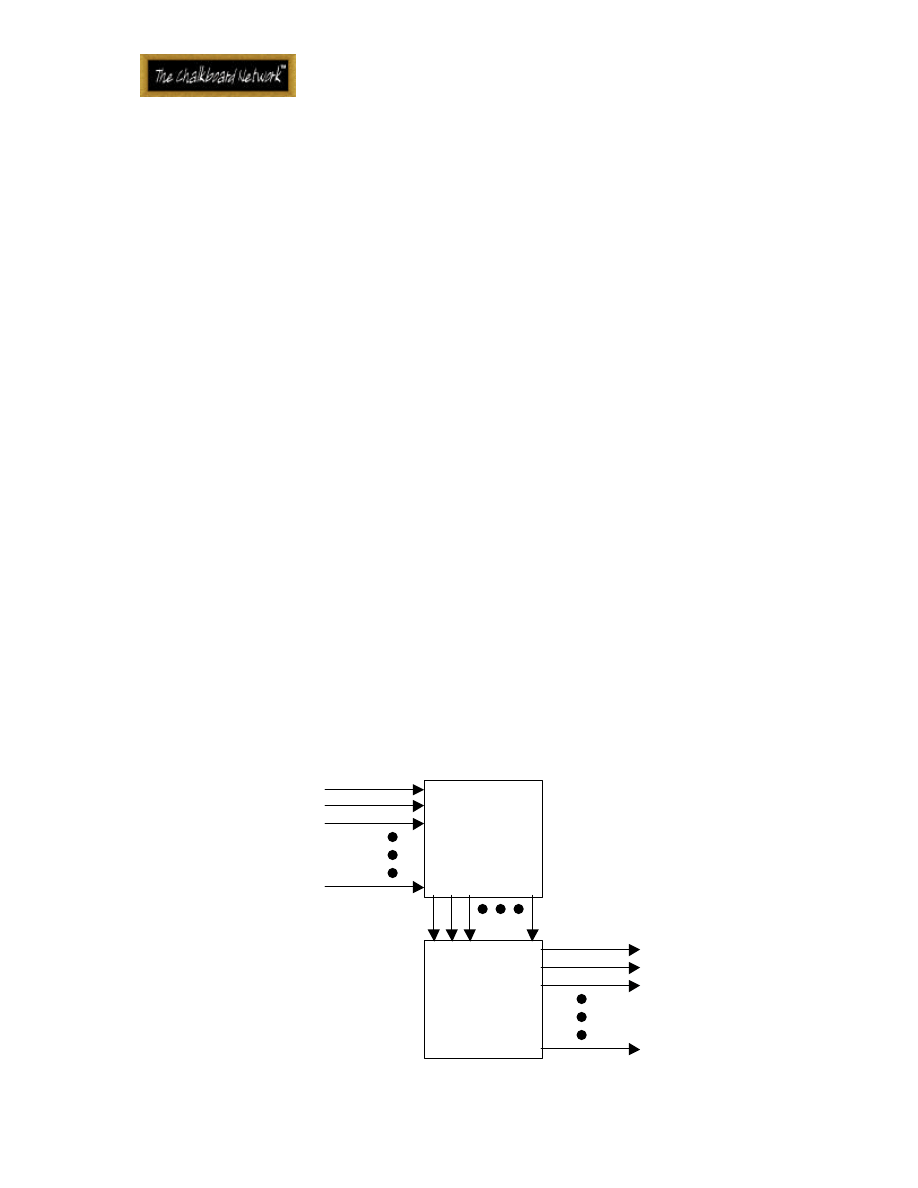
3.2 Programmable Logic Arrays (PLAs)
Programmable Logic Arrays (PLAs) were a solution to the speed and input
limitations of PROMs. PLAs consist of a large number of inputs connected to an
AND plane, where different combinations of signals can be logically ANDed
together according to how the part is programmed. The outputs of the AND
plane go into an OR plane, where the terms are ORed together in different
combinations and finally outputs are produced. At the inputs and outputs there
are typically inverters so that logical NOTs can be obtained. These devices can
implement a large number of combinatorial functions, though not all possible
combinations like a PROM can. However, they generally have many more inputs
and are much faster.
AND
plane
OR
plane
Inputs
Outputs
Introduction to FPGA Design
4
Figure 2 PLA Architecture
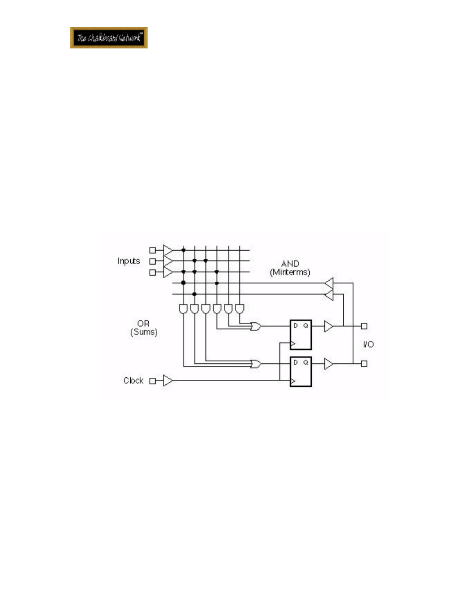
3.3 Programmable Array Logic (PALs)
The Programmable Array Logic (PAL) is a variation of the PLA. Like the
PLA, it has a wide, programmable AND plane for ANDing inputs together.
However, the OR plane is fixed, limiting the number of terms that can be ORed
together. Other basic logic devices, such as multiplexers, exclusive ORs, and
latches are added to the inputs and outputs. Most importantly, clocked
elements, typically flip-flops, are included. These devices are now able to
implement a large number of logic functions including clocked sequential logic
need for state machines. This was an important development that allowed PALs
to replace much of the standard logic in many designs. PALs are also extremely
fast.
Figure 3 PAL Architecture
3.4 CPLDs and FPGAs
Ideally, though, the hardware designer wanted something that gave him
or her the flexibility and complexity of an ASIC but with the shorter turn-around
time of a programmable device. The solution came in the form of two new
devices - the Complex Programmable Logic Device (CPLD) and the Field
Programmable Gate Array. As can be seen in Figure 4, CPLDs and FPGAs bridge
the gap between PALs and Gate Arrays. CPLDs are as fast as PALs but more
complex. FPGAs approach the complexity of Gate Arrays but are still
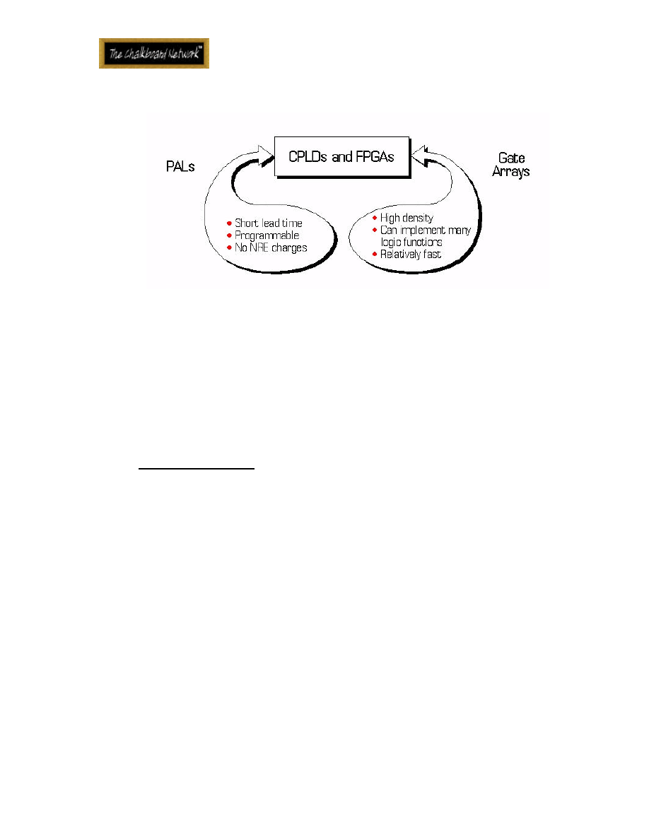
Introduction to FPGA Design
5
programmable.
Figure 4 Comparison of CPLDs and FPGAs
3.5 Complex Programmable Logic Devices (CPLDs)
Complex Programmable Logic Devices (CPLDs) are exactly what they
claim to be. Essentially they are designed to appear just like a large number of
PALs in a single chip, connected to each other through a crosspoint switch They
use the same development tools and programmers, and are based on the same
technologies, but they can handle much more complex logic and more of it.
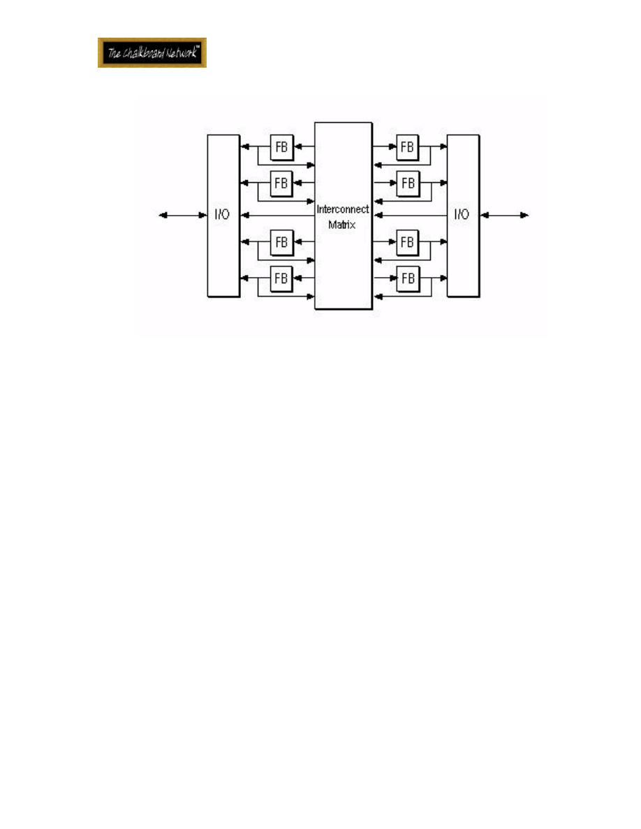
3.5.1 CPLD Architectures
The diagram in Figure 5 shows the internal architecture of a typical
CPLD. While each manufacturer has a different variation, in general they are all
similar in that they consist of function blocks, input/output block, and an
interconnect matrix. The devices are programmed using programmable
elements that, depending on the technology of the manufacturer, can be
EPROM cells, EEPROM cells, or Flash EPROM cells.
Introduction to FPGA Design
6
Figure 5 CPLD Architecture
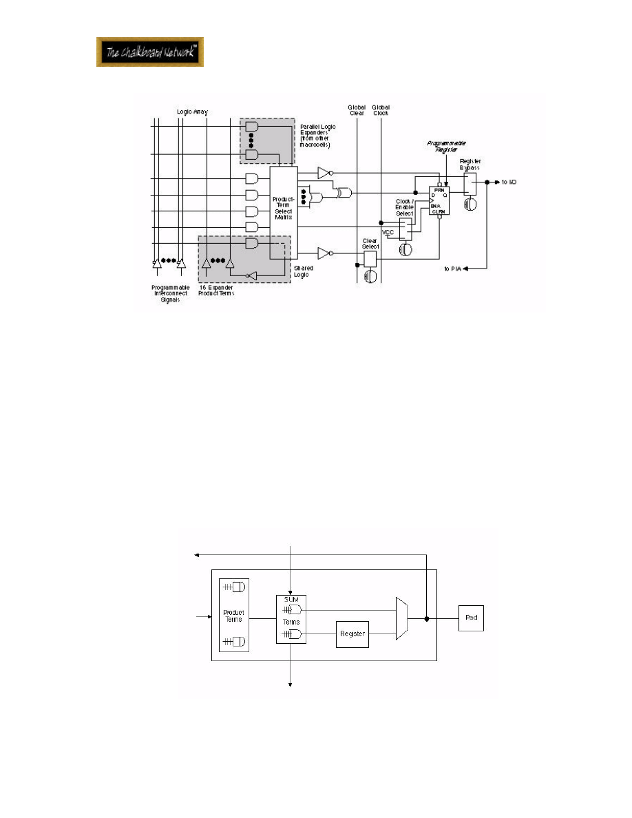
3.5.1.1 Function Blocks
A typical function block is shown in Figure 6. The AND plane still exists as
shown by the crossing wires. The AND plane can accept inputs from the I/O
blocks, other function blocks, or feedback from the same function block. The
terms and then ORed together using a fixed number of OR gates, and terms are
selected via a large multiplexer. The outputs of the mux can then be sent
straight out of the block, or through a clocked flip-flop. This particular block
includes additional logic such as a selectable exclusive OR and a master reset
signal, in addition to being able to program the polarity at different stages.
Usually, the function blocks are designed to be similar to existing PAL
architectures, such as the 22V10, so that the designer can use familiar tools or
even older designs without changing them.
Introduction to FPGA Design
7
Figure 6 CPLD Function Block
3.5.1.2 I/O Blocks
Figure 7 shows a typical I/O block of a CPLD. The I/O block is used to
drive signals to the pins of the CPLD device at the appropriate voltage levels
with the appropriate current. Usually, a flip-flop is included, as shown in the
figure. This is done on outputs so that clocked signals can be output directly to
the pins without encountering significant delay. It is done for inputs so that
there is not much delay on a signal before reaching a flip-flop which would
increase the device hold time requirement. Also, some small amount of logic is
included in the I/O block simply to add some more resources to the device.
Figure 7 CPLD Input/Output Block

Introduction to FPGA Design
8
3.5.1.3 Interconnect
The CPLD interconnect is a very large programmable switch matrix that
allows signals from all parts of the device go to all other parts of the device.
While no switch can connect all internal function blocks to all other function
blocks, there is enough flexibility to allow many combinations of connections.
3.5.1.4 Programmable Elements
Different manufacturers use different technologies to implement the
programmable elements of a CPLD. The common technologies are Electrically
Programmable Read Only Memory (EPROM), Electrically Erasable PROM
(EEPROM) and Flash EPROM. These technologies are similar to, or next
generation versions of, the technologies that were used for the simplest
programmable devices, PROMs.
3.5.2 CPLD Architecture Issues
When considering a CPLD for use in a design, the following issues should
be taken into account:
1. The programming technology
•
EPROM, EEPROM, or Flash EPROM? This will determine the
equipment needed to program the devices and whether they
came be programmed only once or many times.
2. The function block capability
•
How many function blocks are there in the device?
•
How many product and sum terms can be used?
•
What are the minimum and maximum delays through the logic?
•
What additional logic resources are there such as XNORs, ALUs,
etc.?
•
What kind of register controls are available (e.g., clock
enable, reset, preset, polarity control)? How many are local
inputs to the function block and how many are global, chip-
wide inputs?
•
What kind of clock drivers are in the device and what is the
worst case skew of the clock signal on the chip. This will help
determine the maximum frequency at which the device can
run.
3. The I/O capability
•
How many I/O are independent, used for any function, and

Introduction to FPGA Design
9
how many are dedicated for clock input, master reset, etc.?
•
What is the output drive capability in terms of voltage levels
and current?
•
What kind of logic is included in an I/O block that can be used
to increase the functionality of the design?
3.5.3 Example CPLD Families
Some CPLD families from different vendors are listed below:
•
Altera MAX 7000 and MAX 9000 families
•
Atmel ATF and ATV families
•
Lattice ispLSI family
•
Lattice (Vantis) MACH family
•
Xilinx XC9500 family
3.6 Field Programmable Gate Arrays (FPGAs)
Field Programmable Gate Arrays are called this because rather than
having a structure similar to a PAL or other programmable device, they are
structured very much like a gate array ASIC. This makes FPGAs very nice for use
in prototyping ASICs, or in places where and ASIC will eventually be used. For
example, an FPGA maybe used in a design that need to get to market quickly
regardless of cost. Later an ASIC can be used in place of the FPGA when the
production volume increases, in order to reduce cost.
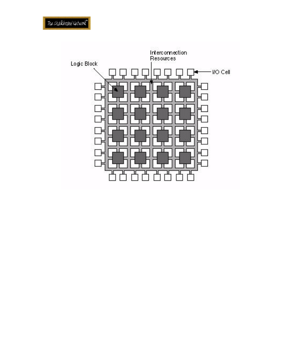
3.6.1 FPGA Architectures
Introduction to FPGA Design
10
Figure 8 FPGA Architecture
Each FPGA vendor has its own FPGA architecture, but in general terms
they are all a variation of that shown in Figure 8. The architecture consists of
configurable logic blocks, configurable I/O blocks, and programmable
interconnect. Also, there will be clock circuitry for driving the clock signals to
each logic block, and additional logic resources such as ALUs, memory, and
decoders may be available. The two basic types of programmable elements for
an FPGA are Static RAM and anti-fuses.
3.6.1.1 Configurable Logic Blocks
Configurable Logic Blocks contain the logic for the FPGA. In a large grain
architecture, these CLBs will contain enough logic to create a small state
machine. In a fine grain architecture, more like a true gate array ASIC, the CLB
will contain only very basic logic. The diagram in Figure 9 would be considered
a large grain block. It contains RAM for creating arbitrary combinatorial logic
functions. It also contains flip-flops for clocked storage elements, and
multiplexers in order to route the logic within the block and to and from
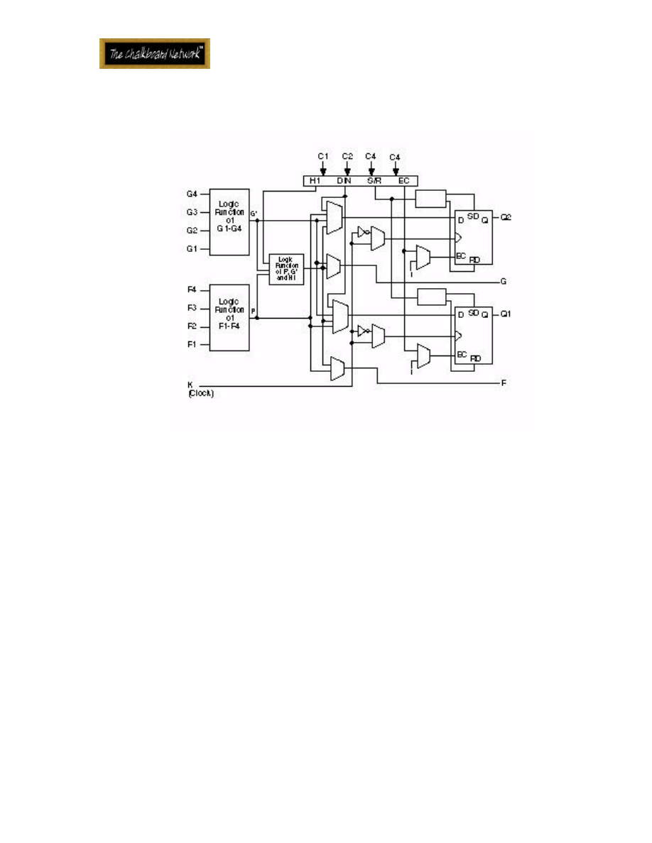
Introduction to FPGA Design
11
external resources. The muxes also allow polarity selection and reset and clear
input selection.
Figure 9 FPGA Configurable Logic Block
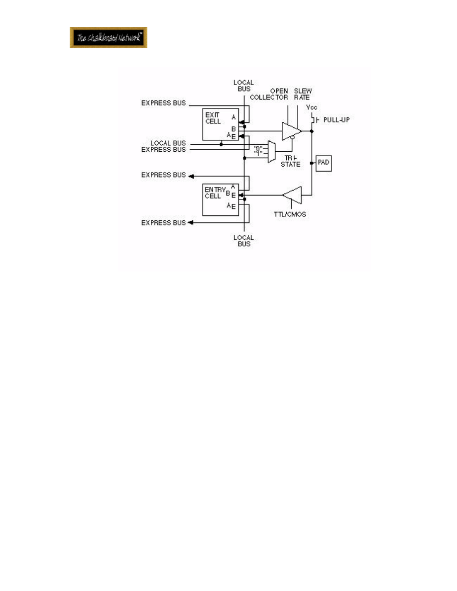
3.6.1.2 Configurable I/O Blocks
A Configurable I/O Block, shown in Figure 10, is used to bring signals onto
the chip and send them back off again. It consists of an input buffer and an
output buffer with three state and open collector output controls. Typically
there are pull up resistors on the outputs and sometimes pull down resistors.
The polarity of the output can usually be programmed for active high or active
low output and often the slew rate of the output can be programmed for fast or
slow rise and fall times. In addition, there is often a flip-flop on outputs so that
clocked signals can be output directly to the pins without encountering
significant delay. It is done for inputs so that there is not much delay on a signal
before reaching a flip-flop which would increase the device hold time
requirement.
Introduction to FPGA Design
12
Figure 10 FPGA Configurable I/O Block
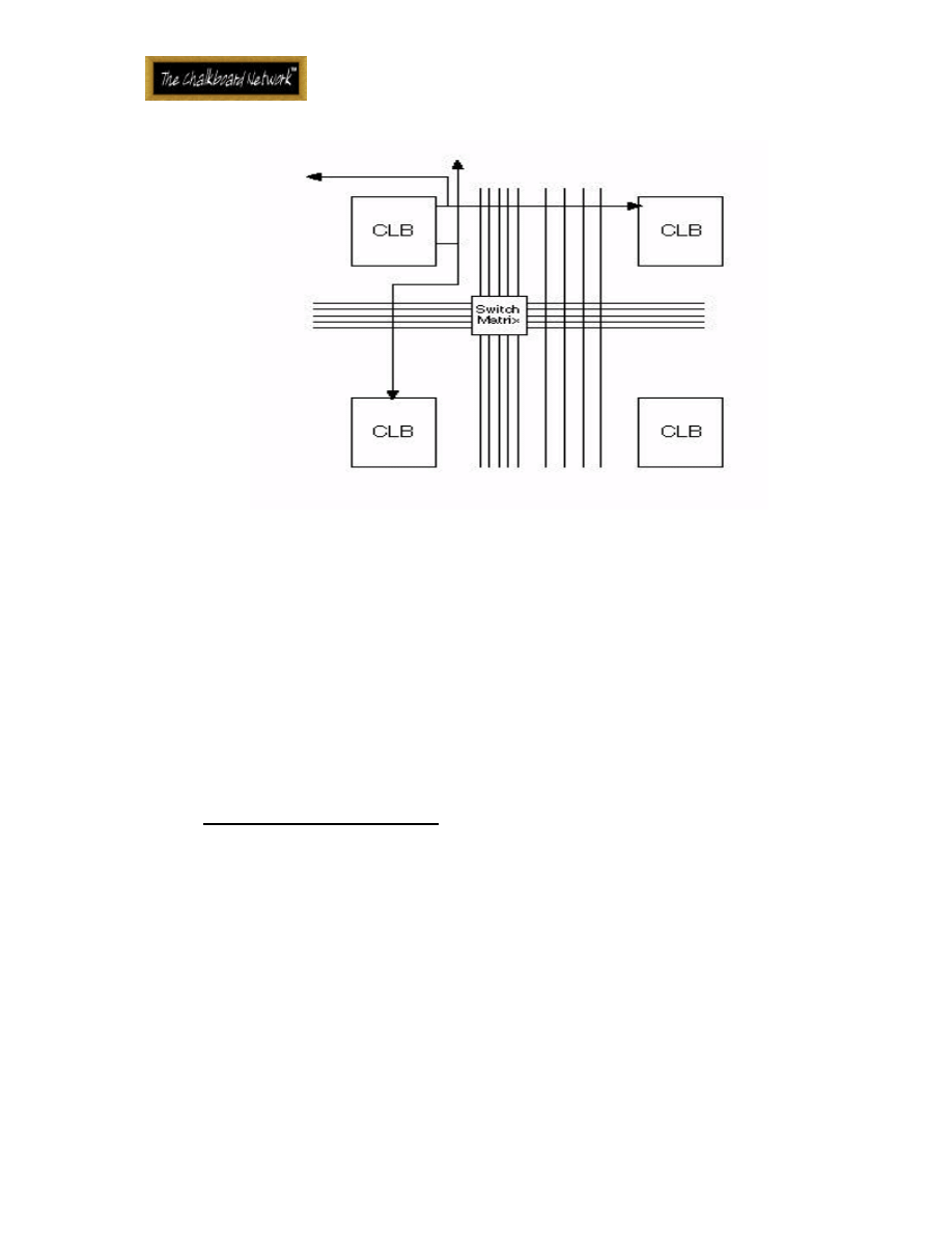
3.6.1.3 Programmable Interconnect
The interconnect of an FPGA is very different than that of a CPLD, but is
rather similar to that of a gate array ASIC. In Figure 11, a hierarchy of
interconnect resources can be seen. There are long lines which can be used to
connect critical CLBs that are physically far from each other on the chip
without inducing much delay. They can also be used as buses within the chip.
There are also short lines which are used to connect individual CLBs which are
located physically close to each other. There is often one or several switch
matrices, like that in a CPLD, to connect these long and short lines together in
specific ways. Programmable switches inside the chip allow the connection of
CLBs to interconnect lines and interconnect lines to each other and to the
switch matrix. Three-state buffers are used to connect many CLBs to a long
line, creating a bus. Special long lines, called global clock lines, are specially
designed for low impedance and thus fast propagation times. These are
connected to the clock buffers and to each clocked element in each CLB. This
is how the clocks are distributed throughout the FPGA.
Introduction to FPGA Design
13
Figure 11 FPGA Programmable Interconnect
3.6.1.4 Clock Circuitry
Special I/O blocks with special high drive clock buffers, known as clock
drivers, are distributed around the chip. These buffers are connect to clock
input pads and drive the clock signals onto the global clock lines described
above. These clock lines are designed for low skew times and fast propagation
times. As we will discuss later, synchronous design is a must with FPGAs, since
absolute skew and delay cannot be guaranteed. Only when using clock signals
from clock buffers can the relative delays and skew times be guaranteed.
3.6.2 Small vs. Large Granularity
Small grain FPGAs resemble ASIC gate arrays in that the CLBs contain only
small, very basic elements such as NAND gates, NOR gates, etc. The philosophy
is that small elements can be connected to make larger functions without
wasting too much logic. In a large grain FPGA, where the CLB can contain two
or more flip-flops, a design which does not need many flip-flops will leave
many of them unused. Unfortunately, small grain architectures require much
more routing resources, which take up space and insert a large amount of delay
which can more than compensate for the better utilization.

Introduction to FPGA Design
14
Small Granularity
Large Granularity
better utilization
fewer levels of logic
direct conversion to ASIC
less interconnect delay
Table 1 Small vs. Large Grain FPGAs
A comparison of advantages of each type of architecture is shown in
Table 1 above. The choice of which architecture to use is dependent on your
specific application.
3.6.3 SRAM vs. Anti-fuse Programming
There are two competing methods of programming FPGAs. The first,
SRAM programming, involves small Static RAM bits for each programming
element. Writing the bit with a zero turns off a switch, while writing with a
one turns on a switch. The other method involves anti-fuses which consist of
microscopic structures which, unlike a regular fuse, normally makes no
connection. A certain amount of current during programming of the device
causes the two sides of the anti-fuse to connect.
The advantages of SRAM based FPGAs is that they use a standard
fabrication process that chip fabrication plants are familiar with and are always
optimizing for better performance. Since the SRAMs are reprogrammable, the
FPGAs can be reprogrammed any number of times, even while they are in the
system, just like writing to a normal SRAM. The disadvantages are that they are
volatile, which means a power glitch could potentially change it. Also, SRAM-
based devices have large routing delays.
The advantages of Anti-fuse based FPGAs are that they are non-volatile
and the delays due to routing are very small, so they tend to be faster. The
disadvantages are that they require a complex fabrication process, they require
an external programmer to program them, and once they are programmed, they
cannot be changed.
3.6.4 Example FPGA Families
Examples of SRAM based FPGA families include the following:
•
Altera FLEX family
•
Atmel AT6000 and AT40K families
•
Lucent Technologies ORCA family
•
Xilinx XC4000 and Virtex families

Introduction to FPGA Design
15
Examples of Anti-fuse based FPGA families include the following:
•
Actel SX and MX families
•
Quicklogic pASIC family
3.7 Choosing Between CPLDs and FPGAs
Choosing between a CPLD and an FPGA will depend on the
characteristics and requirements of your project. A summary of the
characteristics of each is show in Figure 12 below.
CPLD
FPGA
Architecture
PAL-like
Gate Array-like
Density
Low to medium
12 22V10s or more
Medium to high
up to 1 million gates
Speed
Fast, predictable
Application dependent
Interconnect
Crossbar
Routing
Power Consumption
High
Medium
Figure 12 CPLDs vs. FPGAs
4. THE DESIGN FLOW
This section examines the design flow for any device, whether it is an
ASIC, an FPGA, or a CPLD. This is the entire process for designing a device that
guarantees that you will not overlook any steps and that you will have the best
chance of getting back a working prototype that functions correctly in your
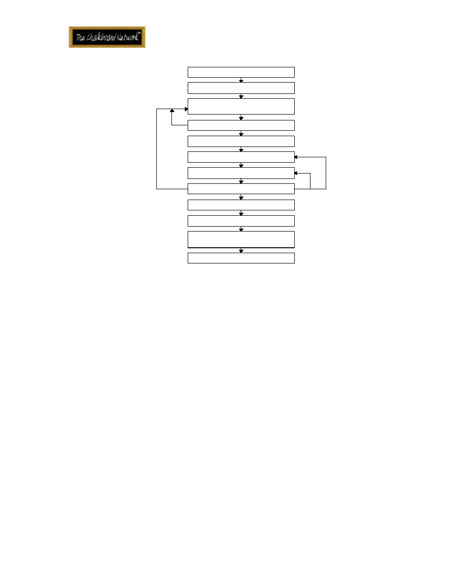
system. The design flow consists of the steps in Figure 13.
Introduction to FPGA Design
16
Write a Specification
Design
Synthesize
Simulate
Resimulate
Place and Route
Chip Test
System Integration and Test
Specification Review
Design Review
Final Review
Ship product!
Figure 13 Design Flow
4.1 Writing a Specification
The importance of a specification cannot be overstated. This is an
absolute must, especially as a guide for choosing the right technology and for
making your needs known to the vendor. As specification allows each engineer
to understand the entire design and his or her piece of it. It allows the engineer
to design the correct interface to the rest of the pieces of the chip. It also
saves time and misunderstanding. There is no excuse for not having a
specification.
A specification should include the following information:
•
An external block diagram showing how the chip fits into the system.
•
An internal block diagram showing each major functional section.
•
A description of the I/O pins including
⇒
output drive capability
⇒
input threshold level
•
Timing estimates including
⇒
setup and hold times for input pins
⇒
propagation times for output pins
⇒
clock cycle time

Introduction to FPGA Design
17
•
Estimated gate count
•
Package type
•
Target power consumption
•
Target price
•
Test procedures
It is also very important to understand that this is a living document.
Many sections will have best guesses in them, but these will change as the chip
is being designed.
4.1.1 Choosing a Technology
Once a specification has been written, it can be used to find the best
vendor with a technology and price structure that best meets your
requirements.
4.1.2 Choosing a Design Entry Method
You must decide at this point which design entry method you prefer. For
smaller chips, schematic entry is often the method of choice, especially if the
design engineer is already familiar with the tools. For larger designs, however,
a hardware description language (HDL) such as Verilog or VHDL is used because
of its portability, flexibility, and readability. When using a high level language,
synthesis software will be required to “synthesize” the design. This means that
the software creates low level gates from the high level description.
4.1.3 Choosing a Synthesis Tool
You must decide at this point which synthesis software you will be using
if you plan to design the FPGA with an HDL. This is important since each
synthesis tool has recommended or mandatory methods of designing hardware
so that it can correctly perform synthesis. It will be necessary to know these
methods up front so that sections of the chip will not need to be redesigned
later on.
At the end of this phase it is very important to have a design review. All
appropriate personnel should review the decisions to be certain that the
specification is correct, and that the correct technology and design entry
method have been chosen.
4.2 Designing the chip

Introduction to FPGA Design
18
It is very important to follow good design practices. This means taking
into account the following design issues that we discuss in detail later in this
paper.
•
Top-down design
•
Use logic that fits well with the architecture of the device you have
chosen
•
Macros
•
Synchronous design
•
Protect against metastability
•
Avoid floating nodes
•
Avoid bus contention
4.3 Simulating - design review
Simulation is an ongoing process while the design is being done. Small
sections of the design should be simulated separately before hooking them up
to larger sections. There will be many iterations of design and simulation in
order to get the correct functionality.
Once design and simulation are finished, another design review must
take place so that the design can be checked. It is important to get others to
look over the simulations and make sure that nothing was missed and that no
improper assumption was made. This is one of the most important reviews
because it is only with correct and complete simulation that you will know that
your chip will work correctly in your system.
4.4 Synthesis
If the design was entered using an HDL, the next step is to synthesize the
chip. This involves using synthesis software to optimally translate your register
transfer level (RTL) design into a gate level design that can be mapped to logic
blocks in the FPGA. This may involve specifying switches and optimization
criteria in the HDL code, or playing with parameters of the synthesis software
in order to insure good timing and utilization.
4.5 Place and Route
The next step is to lay out the chip, resulting in a real physical design for
a real chip. This involves using the vendor’s software tools to optimize the
programming of the chip to implement the design. Then the design is
programmed into the chip.

Introduction to FPGA Design
19
4.6 Resimulating - final review
After layout, the chip must be resimulated with the new timing numbers
produced by the actual layout. If everything has gone well up to this point, the
new simulation results will agree with the predicted results. Otherwise, there
are three possible paths to go in the design flow. If the problems encountered
here are significant, sections of the FPGA may need to be redesigned. If there
are simply some marginal timing paths or the design is slightly larger than the
FPGA, it may be necessary to perform another synthesis with better constraints
or simply another place and route with better constraints. At this point, a final
review is necessary to confirm that nothing has been overlooked.
4.7 Testing
For a programmable device, you simply program the device and
immediately have your prototypes. You then have the responsibility to place
these prototypes in your system and determine that the entire system actually
works correctly. If you have followed the procedure up to this point, chances
are very good that your system will perform correctly with only minor
problems. These problems can often be worked around by modifying the system
or changing the system software. These problems need to be tested and
documented so that they can be fixed on the next revision of the chip. System
integration and system testing is necessary at this point to insure that all parts
of the system work correctly together.
When the chips are put into production, it is necessary to have some sort
of burn-in test of your system that continually tests your system over some long
amount of time. If a chip has been designed correctly, it will only fail because
of electrical or mechanical problems that will usually show up with this kind of
stress testing.
5. DESIGN ISSUES
In the next sections of this paper, we will discuss those areas that are
unique to FPGA design or that are particularly critical to these devices.
5.1 Top-Down Design
Top-down design is the design method whereby high level functions are
defined first, and the lower level implementation details are filled in later. A
schematic can be viewed as a hierarchical tree as shown in Figure 14. The top
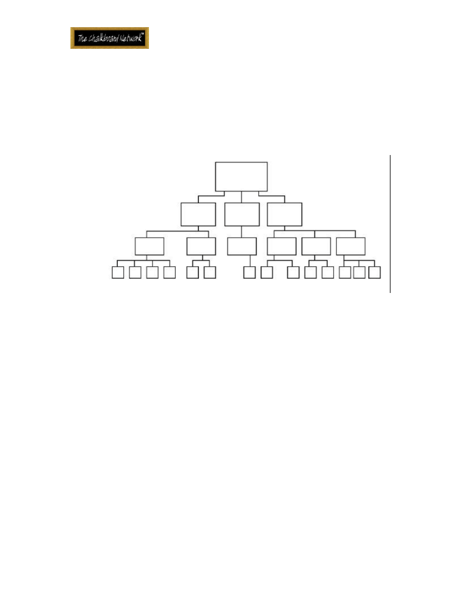
Introduction to FPGA Design
20
level block represents the entire chip. Each lower level block represents major
functions of the chip. Intermediate level blocks may contain smaller
functionality blocks combined with gate-level logic. The bottom level contains
only gates and macrofunctions which are vendor-supplied high level functions.
Fortunately, schematic capture software and hardware description languages
used for chip design easily allows use of the top-down design methodology.
Figure 14 Top-Down Design
Top-down design is the preferred methodology for chip design for
several reasons. First, chips often incorporate a large number of gates and a
very high level of functionality. This methodology simplifies the design task and
allows more than one engineer, when necessary, to design the chip. Second, it
allows flexibility in the design. Sections can be removed and replaced with a
higher-performance or optimized designs without affecting other sections of
the chip.
Also important is the fact that simulation is much simplified using this
design methodology. Simulation is an extremely important consideration in chip
design since a chip cannot be blue-wired after production. For this reason,
simulation must be done extensively before the chip is sent for fabrication. A
top-down design approach allows each module to be simulated independently
from the rest of the design. This is important for complex designs where an
entire design can take weeks to simulate and days to debug. Simulation is
discussed in more detail later in this paper.
5.2 Keep the Architecture in Mind

Introduction to FPGA Design
21
Look at the particular architecture to determine which logic devices fit
best into it. The vendor may be able to offer advice about this. Many synthesis
packages can target their results to a specific FPGA or CPLD family from a
specific vendor, taking advantage of the architecture to provide you with
faster, more optimal designs.
5.3 Synchronous Design
One of the most important concepts in chip design, and one of the
hardest to enforce on novice chip designers, is that of synchronous design.
Once an chip designer uncovers a problem due to asynchronous design and
attempts to fix it, he or she usually becomes an evangelical convert to
synchronous design. This is because asynchronous design problems are due to
marginal timing problems that may appear intermittently, or may appear only
when the vendor changes its semiconductor process. Asynchronous designs that
work for years in one process may suddenly fail when the chip is manufactured
using a newer process.
Synchronous design simply means that all data is passed through
combinatorial logic and flip-flops that are synchronized to a single clock. Delay
is always controlled by flip-flops, not combinatorial logic. No signal that is
generated by combinatorial logic can be fed back to the same group of
combinatorial logic without first going through a synchronizing flip-flop. Clocks
cannot be gated - in other words, clocks must go directly to the clock inputs of
the flip-flops without going through any combinatorial logic.
The following sections cover common asynchronous design problems and
how to fix them using synchronous logic.
5.3.1 Race conditions
Figure 15 shows an asynchronous race condition where a clock signal is
used to reset a flip-flop. When SIG2 is low, the flip-flop is reset to a low state.
On the rising edge of SIG2, the designer wants the output to change to the high
state of SIG1. Unfortunately, since we don’t know the exact internal timing of
the flip-flop or the routing delay of the signal to the clock versus the reset
input, we cannot know which signal will arrive first - the clock or the reset.
This is a race condition. If the clock rising edge appears first, the output will
remain low. If the reset signal appears first, the output will go high. A slight
change in temperature, voltage, or process may cause a chip that works
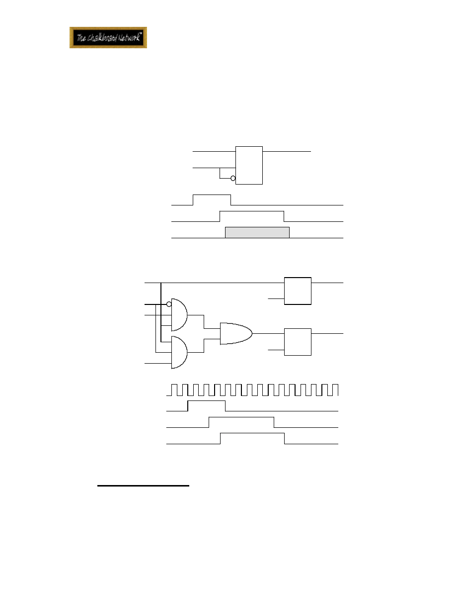
Introduction to FPGA Design
22
correctly to suddenly work incorrectly. A more reliable synchronous solution is
shown in Figure 16. Here a faster clock is used, and the flip-flop is reset on the
rising edge of the clock. This circuit performs the same function, but as long as
SIG1 and SIG2 are produced synchronously - they change only after the rising
edge of CLK - there is no race condition.
D
CLK
Q
CLR
SIG1
SIG2
OUT
SIG1
SIG2
OUT
Figure 15 Asynchronous: Race Condition
D
CLK
Q
SIG2
SIG2d
SIG1
SIG2
OUT
CLK
D
CLK
Q
CLK
OUT
CLK
SIG2d
SIG1
OUT
Figure 16 Synchronous: No Race Condition
5.3.2 Delay dependent logic
Figure 17 shows logic used to create a pulse. The pulse width depends
very explicitly on the delay of the individual logic gates. If the process should
change, making the delay shorter, the pulse width will shorten also, to the
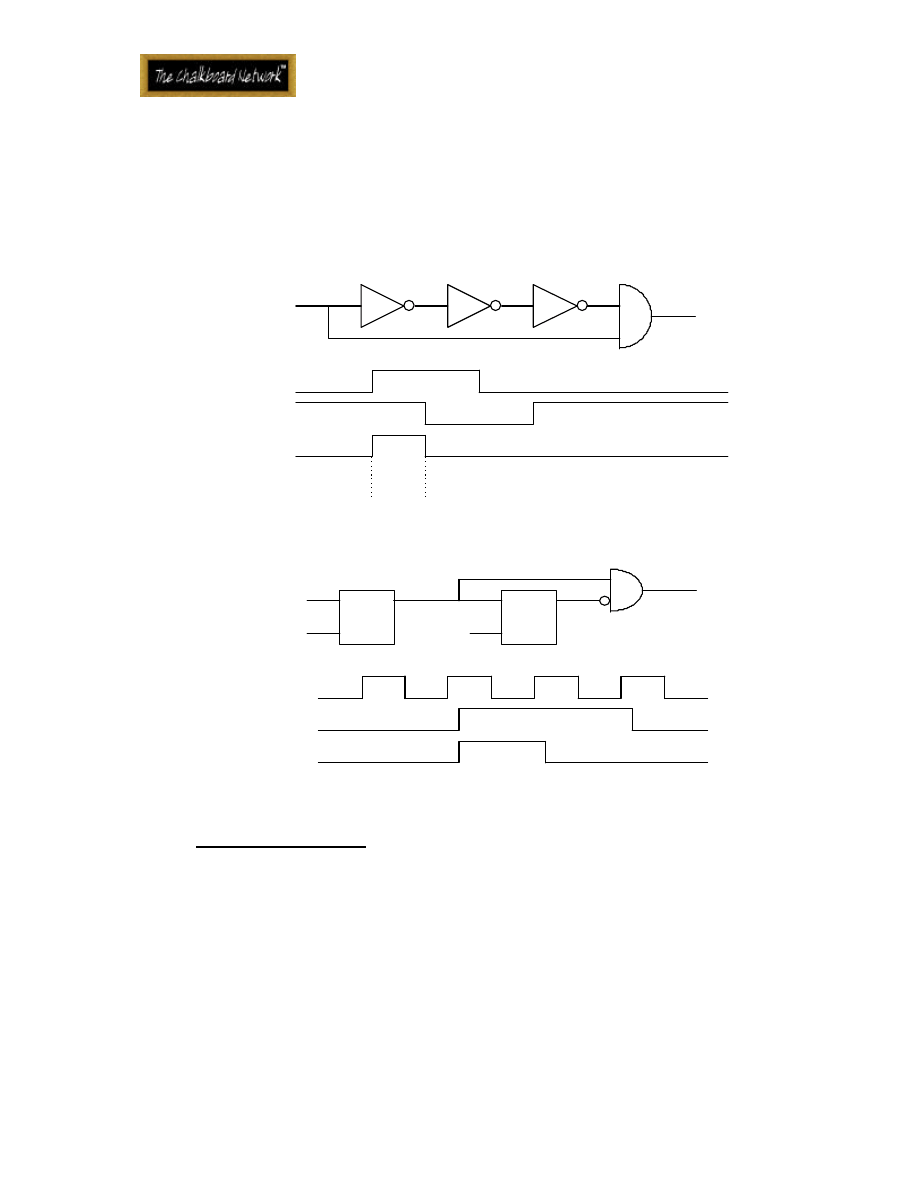
Introduction to FPGA Design
23
point where the logic that it feeds may not recognize it at all. A synchronous
pulse generator is shown in Figure 18. This pulse depends only on the clock
period. Changes to the process will not cause any significant change in the pulse
width.
A
Z
A3
pulse
width
A
A3
Z
A2
A1
Figure 17 Asynchronous: Delay Dependent Logic
D
CLK
Q
A’
D
CLK
Q
CLK
Z
CLK
CLK
A
Z
A
Figure 18 Synchronous: Delay Independent Logic
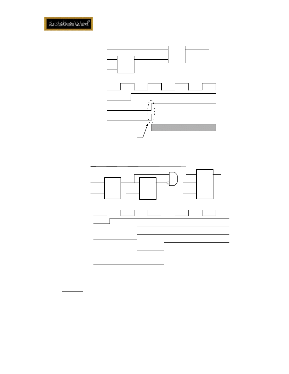
5.3.3 Hold time violations
Figure 19 shows an asynchronous circuit with a hold time violation. Hold
time violations occur when data changes around the same time as the clock
edge. It is uncertain which value will be registered by the clock. The circuit in
Figure 20 fixes this problem by putting both flip-flops on the same clock and
using a flip-flop with an enable input. A pulse generator creates a pulse that
enables the flip-flop.
Introduction to FPGA Design
24
D
CLK
Q
D1
D
CLK
Q
CLK
D2
D3
D4
CLK
D1
D2
D3
D4
Hold time violation
Figure 19 Asynchronous: Hold Time Violation
D2
D1
CLK
CLK
D1
D2
D3
D3p
D4
CLK
D
Q
CLK
D
Q
CLK
D
Q
EN
CLK
CLK
D4
D3
D3p
D3d
D3d
pulse generator
Figure 20 Synchronous: No Hold Time Violation
5.3.4 Glitches
A glitch can occur due to small delays in a circuit such as that shown in
Figure 21. An inverting multiplexer contains a glitch when switching between
two signals, both of which are high. Yet due to the delay in the inverter, the
output goes high for a very short time. Synchronizing this output by sending it
through a flip-flop as shown in Figure 22, ensures that this glitch will not appear
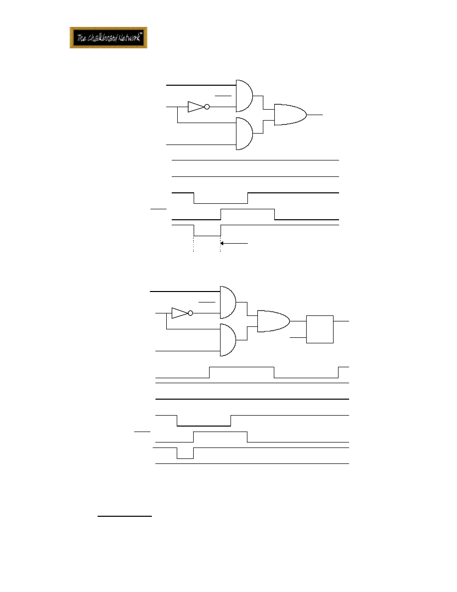
Introduction to FPGA Design
25
on the output and will not affect logic further downstream.
D0
D1
SEL
SEL
D0
SEL
D1
SEL
Z
Z
glitch
Figure 21 Asynchronous: Glitch
D0
D1
SEL
SEL
D0
SEL
D1
SEL
Zp
D
CLK
Q
Z
CLK
Z
Zp
CLK
Figure 22 Synchronous: No Glitch
5.3.5 Bad clocking
Figure 23 shows an example of asynchronous clocking. This kind of
Introduction to FPGA Design
26
clocking will produce problems of the type discussed previously. The correct
way to enable and disable outputs is not by putting logic on the clock input, but
by putting logic on the data input as shown in Figure 24.
CLK
D
CLK
Q
OUT
DATA
GATE
Figure 23 Asynchronous: Bad Clocking
CLK
D
CLK
Q
OUT
DATA
GATE
I0
I1
Figure 24 Synchronous: Good Clocking
5.3.6 Metastability
D
CLK
Q
ASYNC_IN
OUT1
ASYNC_IN
IN
A
CLK
D
CLK
Q
CLK
OUT2
CLK
CLK
A
B
D
CLK
Q
1
1
B
OUT1
OUT2
OUT1 and OUT2 are different
IN

Introduction to FPGA Design
27
Figure 25 Metastability - The Problem
One of the great buzzwords, and often misunderstood concepts, of
synchronous design is metastability. Metastability refers to a condition which
arises when an asynchronous signal is clocked into a synchronous flip-flop. While
chip designers would prefer a completely synchronous world, the unfortunate
fact is that signals coming into a chip will depend on a user pushing a button or
an interrupt from a processor, or will be generated by a clock which is
different from the one used by the chip. In these cases, the asynchronous signal
must be synchronized to the chip clock so that it can be used by the internal
circuitry. The designer must be careful how to do this in order to avoid
metastability problems as shown in Figure 25. If the ASYNC_IN signal goes high
around the same time as the clock, we have an unavoidable race condition.
The output of the flip-flop can actually go to an undefined voltage level that is
somewhere between a logic 0 and logic 1. This is because an internal transistor
did not have enough time to fully charge to the correct level. This metalevel
may remain until the transistor voltage leaks off or “decays”, or until the next
clock cycle. During the clock cycle, the gates that are connected to the output
of the flip-flop may interpret this level differently. In the figure, the upper
gate sees the level as a logic 1 whereas the lower gate sees it as a logic 0. In
normal operation, OUT1 and OUT2 should always be the same value. In this
case, they are not and this could send the logic into an unexpected state from
which it may never return. This metastability can permanently lock up your
chip.
Introduction to FPGA Design
28
D
CLK
Q
OUT1
ASYNC_IN
SYNC_IN
A
CLK
D
CLK
Q
CLK
OUT2
CLK
CLK
A
B
D
CLK
Q
1
1
B
OUT1
OUT2
ASYNC_IN
CLK
D
CLK
Q
SYNC_IN
IN
IN
synchronizer
Figure 26 Metastability - The "Solution"
The “solution” to this metastability problem is shown in Figure 26. By
placing a synchronizer flip-flop in front of the logic, the synchronized input will
be sampled by only one device, the second flip-flop, and be interpreted only as
a logic 0 or 1. The upper and lower gates will both sample the same logic level,
and the metastability problem is avoided. Or is it? The word solution is in
quotation marks for a very good reason. There is a very small but non-zero
probability that the output of the synchronizer flip-flop will not decay to a
valid logic level within one clock period. In this case, the next flip-flop will
sample an indeterminate value, and there is again a possibility that the output
of that flip-flop will be indeterminate. At higher frequencies, this possibility is
greater. Unfortunately, there is no certain solution to this problem. Some
vendors provide special synchronizer flip-flops whose output transistors decay
very quickly. Also, inserting more synchronizer flip-flops reduces the probability
of metastability but it will never reduce it to zero. The correct action involves
discussing metastability problems with the vendor, and including enough
synchronizing flip-flops to reduce the probability so that it is unlikely to occur
within the lifetime of the product.

Introduction to FPGA Design
29
Notice that each synchronizer flip-flop may delay the logic level change
on the input by one clock cycle before it is recognized by the internal circuitry
of the chip. Given that the external signal is asynchronous, by definition this is
not a problem since the exact time that it is asserted will not be deterministic.
If this delay is a problem, then most likely the entire system will need to be
synchronized to a single clock.
5.3.7 Allowable uses of asynchronous logic
Now that I’ve gone through a long argument against asynchronous design,
I will tell you the few exceptions that I have found to this rule. These
exceptions, however, must be designed with extreme caution and only as a last
resort when a synchronous solution cannot be found.
5.3.7.1 Asynchronous reset
There are times when an asynchronous reset is acceptable, or even
preferred. If the vendor’s library includes asynchronously resettable flip-flops,
the reset input can be tied to a master reset in order to reduce the routing
congestion and to reduce the logic required for a synchronous reset. FPGAs and
CPLDs will typically have master reset signals built into the architecture. Using
these signals to reset state machines frees up interconnect for other uses.
Asynchronous reset should be used only for resetting the entire chip and
should not occur during normal functioning of the chip. After reset, you must
ensure that the chip is in a stable state such that no flip-flops will change until
an input changes. You must also ensure that the inputs to the chip are stable and
will not change for at least one clock cycle after the reset is removed.
5.3.7.2 Asynchronous latches on inputs
Some buses, such as the VME bus, are designed to be asynchronous. In
order to interface with these buses, it is necessary to use asynchronous latches
to capture addresses or data. Once the data is captured, it must be
synchronized to the internal clock. However, it is usually much more efficient
to use asynchronous latches to capture the data initially. Unless your chip uses a
clock which has a frequency much higher than that of the bus, attempting to
synchronously latch these signals will cause a large amount of overhead and may
actually produce timing problems rather than reduce them.
5.4 Floating Nodes
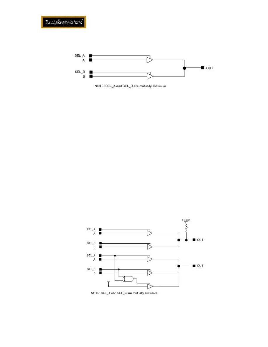
Introduction to FPGA Design
30
Figure 27 Floating Nodes - The Problem
Floating nodes, or internal nodes of a circuit which are not continually
driven, should be avoided. An example of a potential floating node is shown in
Figure 27. If signals SEL_A and SEL_B are both not asserted, signal OUT will float
to an unknown level. Downstream logic may interpret OUT as a logic 1, a logic
0, or it may produce a metastable state. In addition, any CMOS circuitry that
has OUT as an input will use up power since CMOS uses power when the input is
in the threshold region.
Two solutions to the floating node problem are shown in Figure 28. At
the top, signal OUT is pulled up using an internal pull-up resistor. This ensures
that when both select signals are not asserted, OUT will be pulled to a good
logic level. The other solution, shown at the bottom of the figure, is to make
sure that something is driving the output at all times. A third select is generated
which drives the output to a good level when neither of the select signals are
asserted.
Figure 28 Floating Nodes - Solutions
Introduction to FPGA Design
31
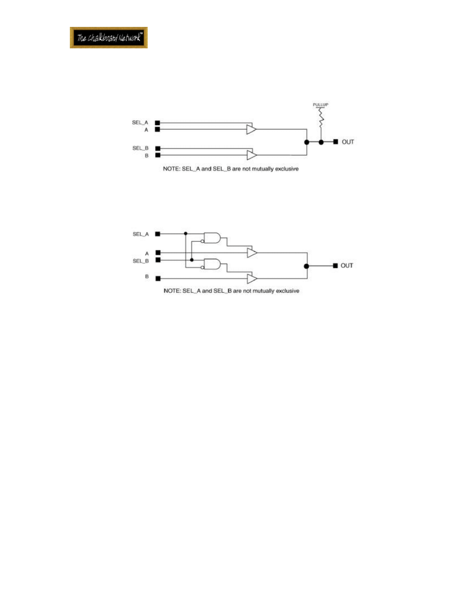
5.5 Bus Contention
Figure 29 Bus Contention - The Problem
Figure 30 Bus Contention - The Solution
Bus contention occurs when two outputs drive the same signal at the
same time as shown in Figure 29. For obvious reasons, this is bad and reduces
the reliability of the chip. If bus contention occurs even for short times during a
clock cycle, after many clock cycles the possibility of damage to one of the
drivers increases. The solution is to ensure that both drivers cannot be asserted
simultaneously. This can be accomplished by inserting additional logic as shown
in Figure 30. The ideal solution is to avoid tri-state drivers altogether, and use
muxes whenever possible.
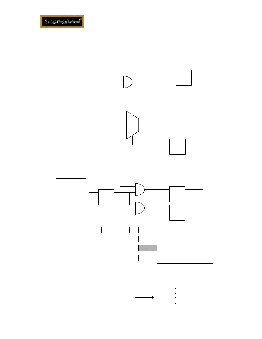
5.6 One-Hot State Encoding
For large grain FPGAs, which are the majority of architectures available,
the normal method of designing state machines is not optimal. This is because
the each CLB in an FPGA has one or more flip-flops, making for an abundance of
flip-flops. For large combinatorial logic terms, however, many CLBs are often
involved which means connecting these CLBs through slow interconnect. A
typical state machine design, like the one shown in Figure 31, uses few flip-
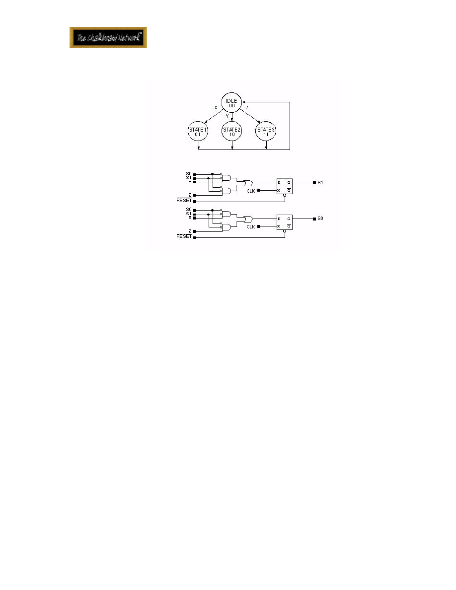
Introduction to FPGA Design
32
flops and much combinatorial logic. This is good for ASICs, bad for FPGAs.
Figure 31 State Machine: Usual Method
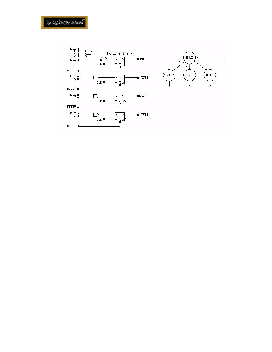
The better method of designing state machines for FPGAs is known as
one-hot encoding, seen in Figure 32. Using this method, each state is
represented by a single flip-flop, rather than encoded from several flip-flop
outputs. This greatly reduces the combinatorial logic, since only one bit needs
to be checked to see if the state machine is in a particular state. It is important
to note that each state bit flip-flop needs to be reset when initialized, except
for the IDLE state flip-flop which needs to be set so that the state machine
begins in the IDLE state.
Introduction to FPGA Design
33
Figure 32 State Machine: One-Hot Encoding
6. DESIGN FOR TEST (DFT)
“Design for test” is a concept which means your chip is designed in such
a way that testing it is easy. Test logic plays two roles. First, it helps debug a
chip which has design flaws. Second, it can catch manufacturing problems. Both
are particularly important for ASIC design because of the black box nature of
ASICs where internal nodes are simply not accessible to you when there is a
problem. These techniques are also applicable to CPLDs and FPGAs, many of
which already have built-in test features. The following DFT techniques allow
for better testing of a chip. While not all of these techniques need to be
included in your design, those that are needed should be included at design
time. DFT techniques should be taken into account during the design process
rather than afterwards. Otherwise, circuits can be designed that are later found
to be difficult, if not impossible, to test.
One important consideration that can be overlooked, is that test logic is
intended to increase the testability and reliability of your chip. If test logic
becomes too large, it can actually decrease reliability because the test logic can
itself have problems which cause the chip to malfunction. A rule of thumb is
that test circuitry should not make up more than 10% of the logic of the entire
chip. Similarly, if you spend more than 10% of your time designing and
simulating your test logic independently of the functionality of the chip, then
you have more test circuitry than you need.
Introduction to FPGA Design
34
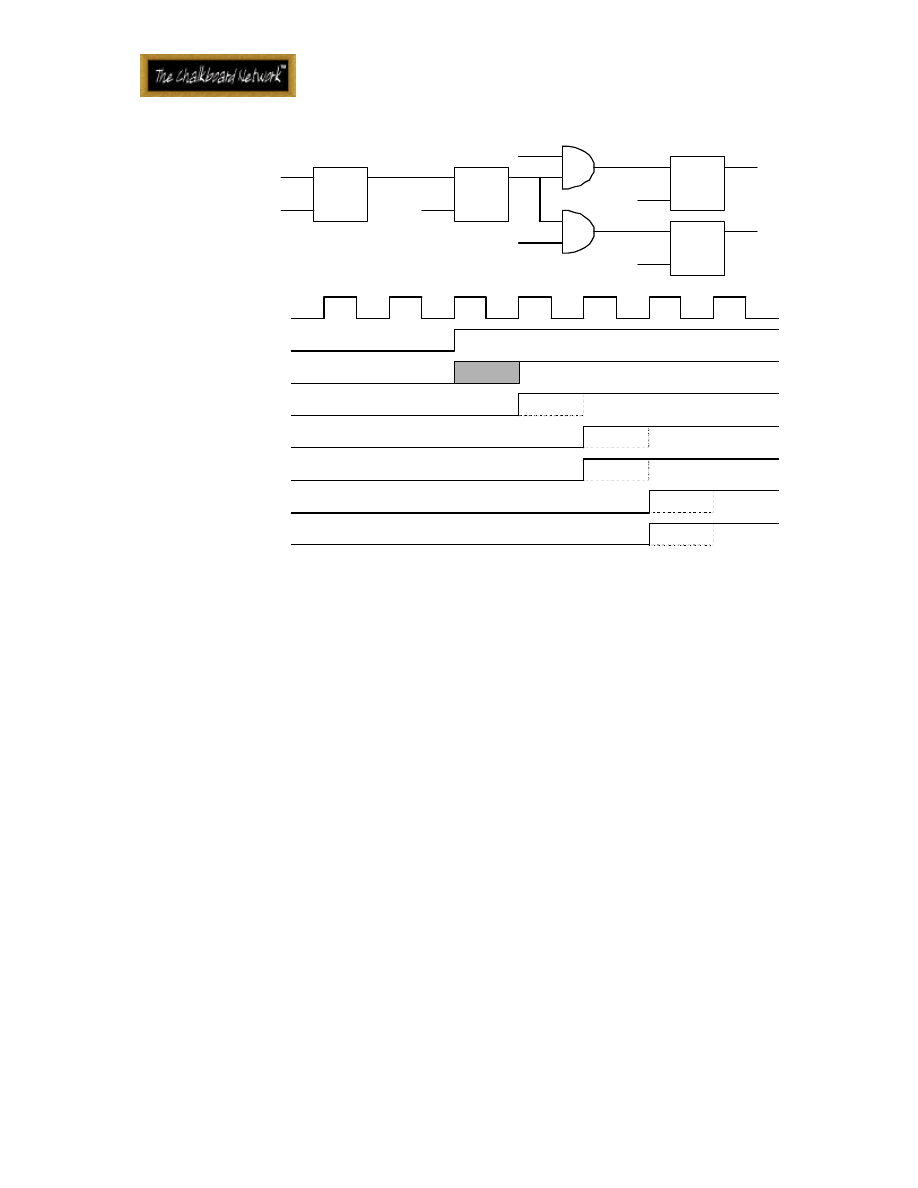
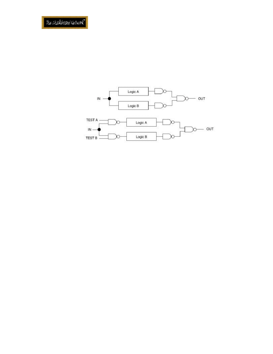
6.1 Testing Redundant Logic
The top of Figure 33 shows a circuit which has duplicated logic in order
to increase the reliability of the design. However, since the circuit is not
testable, the effect is not as useful as it could be. The circuit on the bottom
shows how test lines can be added to allow the entire circuit to be tested.
Figure 33 Testing Redundant Logic
6.2 Initializing State Machines
It is important that all state machines, and in fact all registers in your
design be able to be initialized. This ensures that if a problem arises, the chip
can be put into a known state from which to begin debugging. Also, for
simulation purposes, simulation software needs to start out from a known state
before useful results can be obtained.
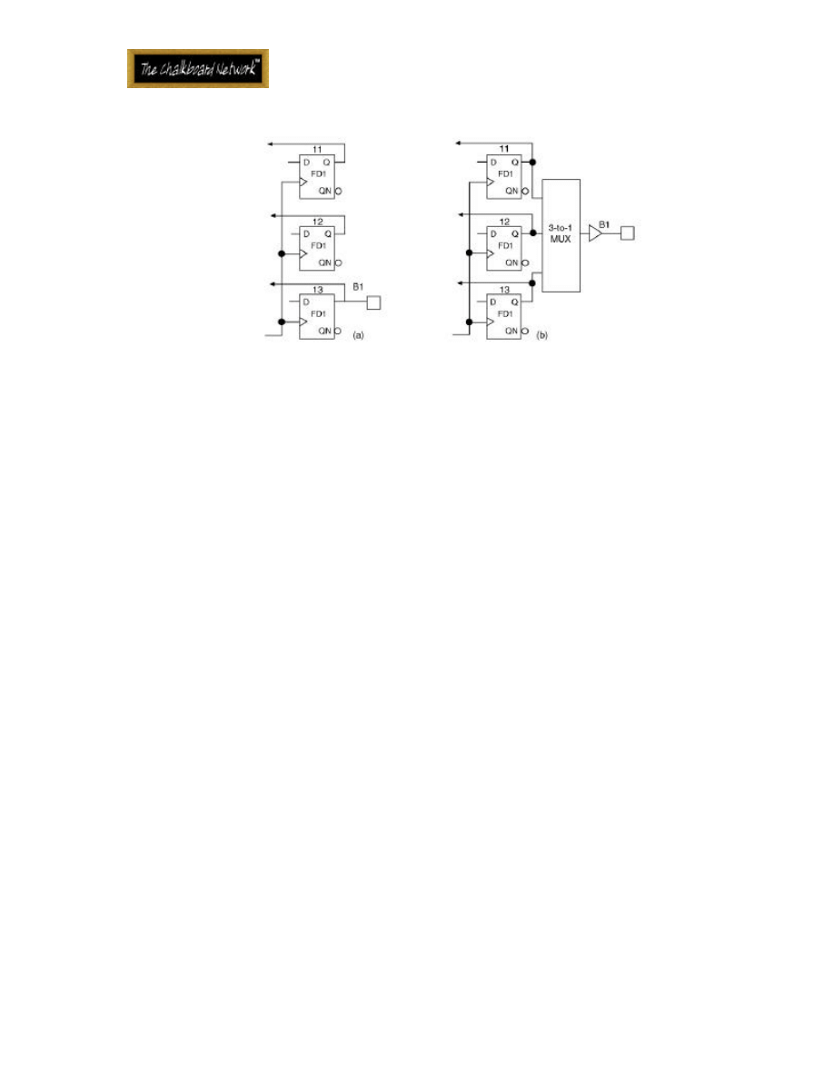
6.3 Observable Nodes
As many nodes as possible in your chip design should be observable. In
other words, it should be possible to determine the values of these nodes using
the I/O pins of the chip. On the left side of Figure 34, an unobservable state
machine is shown. On the right side, the state machine has been made
observable by taking each state machine through a mux to an external pin. Test
signals can be used to select which output is being observed. If no pins are
available, the state bits can be muxed onto an existing pin which, during
testing, is used to observe the state machine. This allows for much easier
debugging of internal state machines.
Introduction to FPGA Design
35
Figure 34 Observable Nodes
6.4 Scan Techniques
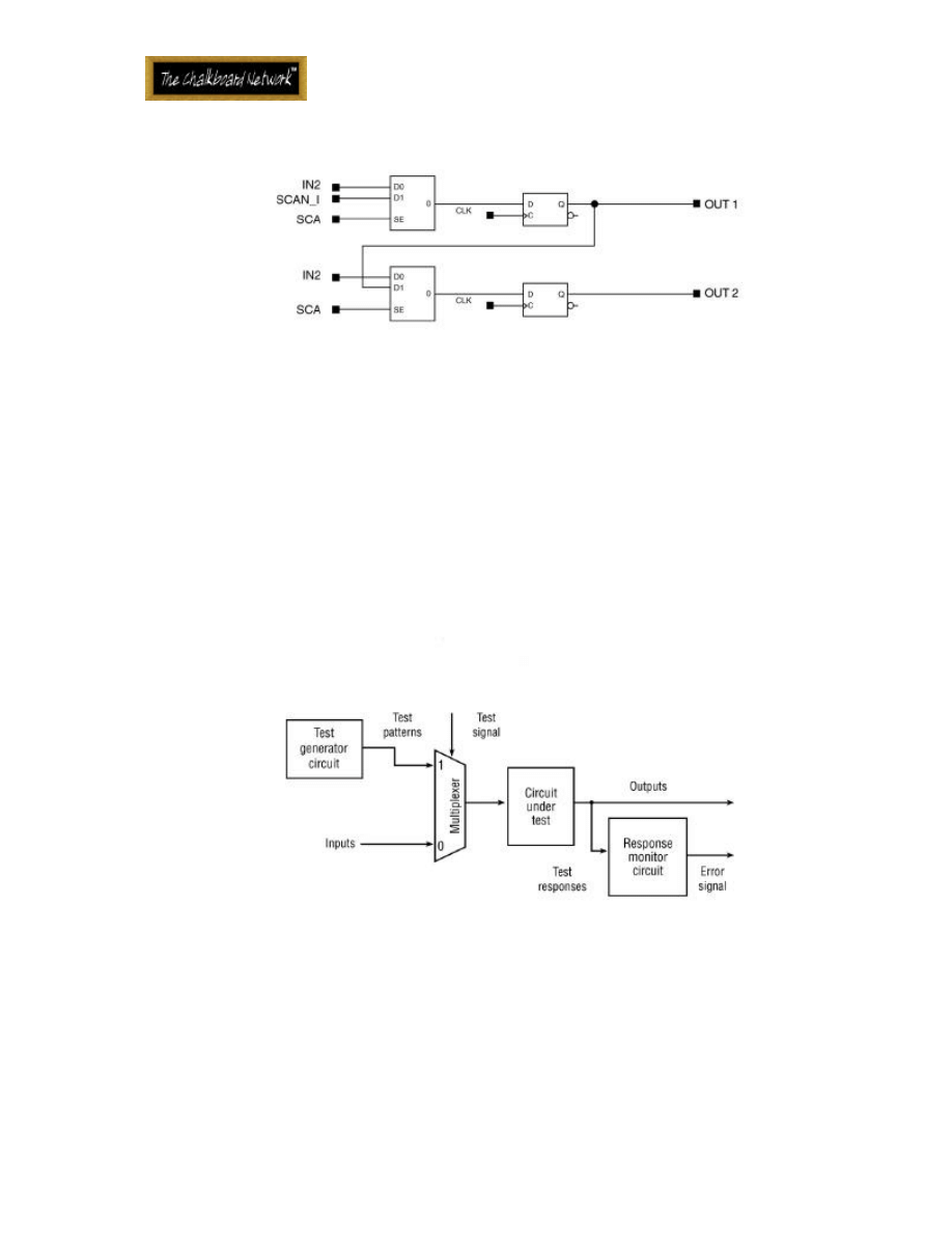
Scan techniques, shown in Figure 35, allow the nodes of the chip to be
scanned out so that they can be observed externally. There are two main scan
techniques - full scan and boundary scan. Full scan is extremely flexible,
especially since it can also allow values to be scanned into the chip so that you
can start it from a known state. This is particularly useful if a problem occurs
only after the chip has been operating for a long time. A state can be quickly
scanned into the chip which corresponds to the state which would normally be
reached after a long time in operation. The drawback of scan techniques are
that they require a lot of software development to support. Also, if states are
scanned into the chip, you must be careful not to scan in illegal states. It is
possible to turn on multiple drivers to a single net internally which would
normally not happen, but which would burn out the chip. Similarly, outputs
must be disabled while the chip is being scanned since dangerous combinations
of outputs may be asserted that can harm your system. There are other
considerations, also, such as what to do with the clock and what to do with the
rest of the system while the chip is being scanned.
Introduction to FPGA Design
36
Figure 35 Scan Methodology
Boundary scan is somewhat easier to implement and does not add as
much logic to the entire chip design. Boundary scan only scans nodes around the
boundary of the chip, but not internal nodes. In this way, internal contention
problems are avoided, although contention problems with the rest of the
system still need to be considered. Boundary scan is also useful for testing the
rest of your system, since the outputs can be toggled and the effect on the rest
of the system observed.
6.5 Built-In Self Test
Figure 36 Built-In Self Test
Another method of testing your chip is to put all of the test circuitry on
the chip in such a way that the chip tests itself. This is called built-in self test
or BIST. In this case, some circuitry inside the chip can be activated by
asserting a special input or combination of inputs. This circuitry then runs a
series of test on the chip. If the result of the tests does not match the

Introduction to FPGA Design
37
expected result, the chip signals that there is a problem. The details of what
type of tests to run and how to signal a good or bad chip is left up to the
designer.
6.6 Signature Analysis
Signature analysis involves putting a pseudo-random sequence of ones and
zeroes into the chip and noting the ones and zeroes that come out. This output
sequence is referred to as the chip’s signature. This type of testing can be
accomplished with the chip in a normal mode of operation, but is usually
performed in scan mode as described above. By repeating the same pseudo-
random series of bits, the resulting signature should be the same for each chip.
Any chip that produces an incorrect signature is a bad chip. This type of testing
is probabilistic and assumes that a pseudo-random sequence of events has a
good chance of catching errors, which may not be true. However, it requires
very little hardware to implement and can be used as a simple form of BIST.
7. SIMULATION ISSUES
Perhaps the most important phase of chip design, and the most often
overlooked phase, is that of simulation. Simulation can save many frustrating
hours debugging a chip in your system. Doing a good job at simulation uncovers
errors before they are set in silicon, and can help determine that your chip will
function correctly in your system.
There are two main aspects of your design for which simulation is used
to determine correctness - functionality and timing. Functionality refers to how
the chip functions as a whole, and how it functions in your system. A chip
which is designed to function as an Ethernet controller may function correctly
on its own. In a system that requires an ATM controller, for example, it will not
work at all. It is important to look not only at the functionality of the chip as an
independent design, but also to test its functionality within the system in which
it will be incorporated.
The second aspect of your design which simulation examines is timing.
Will your chip meet all of its timing requirements under all possible conditions?
Are there any race conditions? Are the setup and hold time requirements met
for each flip-flop? Do the I/O signals of the chip meet the timing requirements
of the system? The following sections discuss ways of using timing to determine
both correct functionality and correct timing.

Introduction to FPGA Design
38
7.1.1 Functional Simulation
Functional simulation involves simulating the functionality of a device
without taking the timing of the device into account. This type of simulation is
important initially in order to get as many bugs out of the device as possible
and to determine that the chip will work correctly in your system. During the
first phases of simulation, you shouldn’t be very concerned about timing
because it will change as the design changes. In fact, the final timing will not
be known precisely until the layout is complete. Of course you need to know
initially that, in general, the timing of the chip process can support the speed
and the I/O requirements of your design.
When performing functional simulation, a rough estimate of the amount
of simulation to perform is called toggle coverage, which measures the
percentage of flip-flops in the chip that change state during simulation. Many
simulation packages will give you a number for the toggle coverage, and you
should have 100 percent coverage before feeling good about the amount of
simulation. This coverage can still leave many potential faults uncovered, but it
signifies that each state machine has been simulated and no part of the circuit
has gone unexamined.
7.1.2 Static Timing Analysis
Static timing analysis is a process that looks at a synchronous design and
determines the highest operating frequency of the design which does not
violate any setup and hold times. You can also use the static timing analysis
software to specify a specific frequency, and the tool will list all paths that
violate the timing requirements. These paths can then be adjusted to meet
your requirements. Any asynchronous parts of your design (they should be few,
if any) must be examined by hand.
Static timing analysis, or some sort of timing analysis must be performed
immediately before layout of your chip. At this point, the timing numbers will
be estimates that take expected trace lengths into account. After layout, timing
analysis must be performed again to determine that the real chip, with real
trace lengths and delays, still meets you timing requirements.
7.1.3 Timing Simulation
This method of timing analysis is growing less and less popular. It involves

Introduction to FPGA Design
39
including timing information in a functional simulation so that the real behavior
of the chip is simulated. The advantage of this kind of simulation, is that timing
and functional problems can be examined and corrected. Also, asynchronous
designs must use this type of analysis because static timing analysis only works
for synchronous designs. This is another reason for designing synchronous chips
only.
As chips become larger, though, this type of compute intensive
simulation takes longer and longer to run. Also, simulations can miss particular
transitions that result in worst case results. This means that certain long delay
paths never get evaluated and a chip with timing problems can pass timing
simulation. If you do need to perform timing simulation, it is important to do
both worst case simulation and best case simulation. The term “best case” can
be misleading. It refers to a chip that, due to voltage, temperature, and
process variations, is operating faster than the typical chip. However, hold
time problems become apparent only during the best case conditions.
8. CONCLUSION
This paper has intended to present an overview of CPLD and FPGA
technologies, and give guidelines for developing a chip based on my experience
designing for a large number of companies and a large number of applications. If
all of these guidelines are followed, the chances of creating a working chip in a
short time at minimum expense is excellent.
Bob Zeidman is the president of The Chalkboard Network, which
provides in-depth Internet based courses on high tech subjects. He has been
working in the electronics industry for over 17 years and is the author of the
textbook, Verilog Designer's Library from Prentice-Hall, as well as a number of
articles on engineering and business. He holds an MSEE from Stanford University,
and a BSEE and a BA in physics from Cornell University.
Wyszukiwarka
Podobne podstrony:
How to Design Programs An Introduction to Computing and Programming Matthias Felleisen
Introduction to Lagrangian and Hamiltonian Mechanics BRIZARD, A J
Introduction to Mechatronics and Measurement Systems
Introduction to Prana and Pranic Healing – Experience of Breath and Energy (Pran
Introduction to Microprocessors and Microcontrollers
Introduction to Lagrangian and Hamiltonian Mechanics BRIZARD, A J
TEXTUALITY Antonio Fruttaldo An Introduction to Cohesion and Coherence
Cannas da Silva A Introduction to symplectic and Hamiltonian geometry (Rio de Janeiro lectures, 2002
Introduction to Lagrangian and Hamiltonian Mechanics BRIZARD, A J
Jonathan Jacobs Dimensions of Moral Theory An Introduction to Metaethics and Moral Psychology 2002
Brizard A J Introduction to Lagrangian and Hamiltonian mechanics (web draft, 2004)(173s) PCtm
1405187654 An Introduction to Science and Technology Studies
Baigent Nick An Introduction to Strategy Proof Mechanism Design
Introduction to Microprocessors and Microcontrollers
Introduction to Translation and Interpretation
An Introduction To Swirl and Daisy FGB by M81170
Introduction to the MOSFET and MOSFET Inverter(1)
więcej podobnych podstron