
PLASMA TV
SERVICE MANUAL
PDF created with FinePrint pdfFactory trial version

i
Plasma TV Service Manual
24/10/2003
TABLE OF CONTENTS
1.
INTRODUCTION
.................................................................................................................................1
2.
TUNER ......................................................................................................................................................1
3.
IF PART (TDA9886)
...........................................................................................................................1
4.
MULTI STANDARD SOUND PROCESSOR
..............................................................................2
5.
4.VIDEO SWITCH TEA6415
............................................................................................................2
6.
AUDIO AMPLIFIER STAGE WITH TDA7265
.............................................................................2
7.
POWER SUPPLY (SMPS)
...............................................................................................................3
8.
MICROCONTROLLER
......................................................................................................................3
9.
SERIAL ACCESS CMOS 4K x 8 (32K bit) EEPROM 24C32A
..............................................3
10. CLASS AB STEREO HEADPHONE DRIVER TDA1308
........................................................3
11. SAW FILTERS
......................................................................................................................................3
12. IC DESCRIPTIONS AND INTERNAL BLOCK DIAGRAM
......................................................4
12.1.
MC44608............................................................................................................................................5
12.1.1.
Description ................................................................................................................................5
12.1.2.
General Features ......................................................................................................................5
12.1.3.
Pin Connections .......................................................................................................................5
12.2.
TCET1102G .......................................................................................................................................6
12.2.1.
Description ................................................................................................................................6
12.2.2.
Applications ..............................................................................................................................6
12.2.3.
13.12.3.Features ........................................................................................................................6
12.3.
TDA9886 ............................................................................................................................................6
12.3.1.
General Description..................................................................................................................6
12.3.2.
Features .....................................................................................................................................6
12.3.3.
Pinning.......................................................................................................................................7
12.4.
TEA6415C..........................................................................................................................................7
12.4.1.
General Description..................................................................................................................7
12.4.2.
Features .....................................................................................................................................7
12.4.3.
Pinning.......................................................................................................................................8
12.5.
SAA3010T..........................................................................................................................................8
12.5.1.
Description ................................................................................................................................8
12.5.2.
Features .....................................................................................................................................8
12.5.3.
Pinning.......................................................................................................................................8
12.6.
24C32A ..............................................................................................................................................9
12.6.1.
Features .....................................................................................................................................9
12.6.2.
Description ................................................................................................................................9
12.6.3.
Pin Function table.....................................................................................................................9
12.6.4.
Functional Descriptions .........................................................................................................10
12.7.
SAA5264 ..........................................................................................................................................10
12.7.1.
Features ...................................................................................................................................10
12.7.2.
General Description................................................................................................................10
12.7.3.
Pin Connections and Short Descriptions.............................................................................10
12.8.
LM317 ..............................................................................................................................................12
12.8.1.
General Description................................................................................................................12
12.8.2.
Features ...................................................................................................................................12
12.9.
ST24LC21 ........................................................................................................................................12
12.9.1.
Description ..............................................................................................................................12
12.9.2.
Features ...................................................................................................................................12
12.9.3.
Pin connections ......................................................................................................................13
12.10.
TLC7733 ..........................................................................................................................................13
12.10.1.
Description ..............................................................................................................................13
12.11.
74LVC257A......................................................................................................................................14
12.11.1.
Features ...................................................................................................................................14
12.11.2.
Description ..............................................................................................................................14
12.11.3.
Pin Description .......................................................................................................................14
12.12.
74LVC14A........................................................................................................................................14
PDF created with FinePrint pdfFactory trial version

ii
Plasma TV Service Manual
24/10/2003
12.12.1.
Features ...................................................................................................................................14
12.12.2.
Applications ............................................................................................................................14
12.12.3.
Description ..............................................................................................................................14
12.12.4.
Pin Description .......................................................................................................................15
12.13.
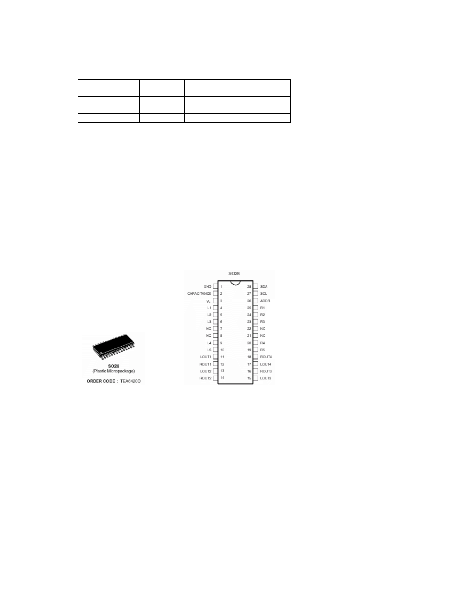
TEA6420 ..........................................................................................................................................15
12.13.1.
Features ...................................................................................................................................15
12.13.2.
Description ..............................................................................................................................15
12.14.
LM1086 ............................................................................................................................................15
12.14.1.
Description ..............................................................................................................................15
12.14.2.
Features ...................................................................................................................................15
12.14.3.
Applications ............................................................................................................................16
12.14.4.
Connection Diagrams.............................................................................................................16
12.15.
LM1117 ............................................................................................................................................16
12.15.1.
General Description................................................................................................................16
12.15.2.
Features ...................................................................................................................................16
12.15.3.
Applications ............................................................................................................................16
12.15.4.
Connection Diagrams.............................................................................................................16
12.16.
DS90C385........................................................................................................................................17
12.16.1.
General Description................................................................................................................17
12.16.2.
Features ...................................................................................................................................17
12.16.3.
Pin Description .......................................................................................................................17
12.17.
TL431 ...............................................................................................................................................18
12.17.1.
Description ..............................................................................................................................18
12.17.2.
Features ...................................................................................................................................18
12.17.3.
Pin Configurations..................................................................................................................18
12.18.
MSP34X1G ......................................................................................................................................19
12.18.1.
Introduction .............................................................................................................................19
12.18.2.
Features ...................................................................................................................................20
12.18.3.
Pin connections ......................................................................................................................20
12.19.
TDA7265 ..........................................................................................................................................22
12.19.1.
Description ..............................................................................................................................22
12.19.2.
Features ...................................................................................................................................22
12.19.3.
Pin Connection .......................................................................................................................22
12.20.
TDA1308 ..........................................................................................................................................22
12.20.1.
General Description................................................................................................................22
12.20.2.
Features ...................................................................................................................................22
12.20.3.
Pinning.....................................................................................................................................23
12.21.
PI5V330 ...........................................................................................................................................23
12.21.1.
General Description................................................................................................................23
12.22.
AD9883A..........................................................................................................................................23
12.22.1.
General Description................................................................................................................23
12.22.2.
Features ...................................................................................................................................23
12.22.3.
Pin Descriptions .....................................................................................................................24
12.23.
SAA7118E........................................................................................................................................26
12.23.1.
General Description................................................................................................................26
12.23.2.
Features ...................................................................................................................................27
12.23.3.
Pinning.....................................................................................................................................28
12.24.
TPS72501 ........................................................................................................................................32
12.24.1.
General Description................................................................................................................32
12.24.2.
Features ...................................................................................................................................32
12.25.
TSOP1836 .......................................................................................................................................33
12.25.1.
Description ..............................................................................................................................33
12.25.2.
Features ...................................................................................................................................33
12.26.
PCF8591 ..........................................................................................................................................33
12.26.1.
General Description................................................................................................................33
12.26.2.
Features ...................................................................................................................................33
12.26.3.
Pinning.....................................................................................................................................34
12.27.
PW1231 ...........................................................................................................................................34
12.27.1.
General Description................................................................................................................34
12.27.2.
Features ...................................................................................................................................34
PDF created with FinePrint pdfFactory trial version

iii
Plasma TV Service Manual
24/10/2003
12.27.3.
Applications ............................................................................................................................35
12.28.
PW181 .............................................................................................................................................35
12.28.1.
General Description................................................................................................................35
12.28.2.
Features ...................................................................................................................................35
12.28.3.
Applications ............................................................................................................................36
12.29.
SIL151B ...........................................................................................................................................36
12.29.1.
General Description................................................................................................................36
12.29.2.
Features ...................................................................................................................................36
12.30.
SDRAM 4M x 16 (MT48LC4M16A2TG-75) .....................................................................................36
12.30.1.
General Description................................................................................................................36
12.30.2.
Features ...................................................................................................................................37
12.30.3.
Pin Descriptions .....................................................................................................................37
12.31.
FLASH 8MBit ...................................................................................................................................39
12.31.1.
Description ..............................................................................................................................39
12.31.2.
Features ...................................................................................................................................39
13. SERVICE MENU SETTINGS
........................................................................................................40
13.1.
display menu ....................................................................................................................................40
13.2.
calibration menu...............................................................................................................................42
13.3.
deinterlacer menu ............................................................................................................................44
13.4.
Service menu factory reset values...................................................................................................46
14. BLOCK DIAGRAM
............................................................................................................................47
15. CIRCUIT DIAGRAMS
......................................................................................................................56
PDF created with FinePrint pdfFactory trial version

1
Plasma TV Service Manual
24/10/2003
1. INTRODUCTION
42” Plasma TV is a progressive TV control system with built-in de-interlacer and scaler. It uses a
852*480 panel with 16:9 aspect ratio.The TV is capable of operation in PAL, SECAM, NTSC (playback)
colour standards and multiple transmission standards as B/G, D/K, I/I’, and L/L´ including German and
NICAM stereo. Sound system output is supplying 2x14W (10%THD) for stereo 8
Ω speakers. The
chassis is equipped with many inputs and outputs allowing it to be used as a center of a media system.
It supports following peripherals:
4 SCART’s with two of them supporting full SCART features including RGB input
2 AV inputs. (CVBS+ Stereo Audio)
1 SVHS iput
1 Streeo Headphone output
1 Subwoofer line level output
1 D-Sub 15 PC input
1 DVI input (Optional)
1 Stereo audio input for PC/DVI
1 LVDS connector for Plasma Display Connection
Other features include, 10 pg Teletext, Picture-In-Picture (PIP) , Picture-And-Picture (PAP) , Picture-
And-Text (PAT) and Picture Zoom.
2. TUNER
The tuners used in the design are combined VHF, UHF tuners suitable for CCIR systems B/G, H, L, L´,
I/I´, and D/K. The tuning is available through the digitally controlled I
2
C bus (PLL). Below you will find
info on one of the Tuners in use.
General description of UV1316:
The UV1316 tuner belongs to the UV 1300 family of tuners, which are designed to meet a wide range of
applications. It is a combined VHF, UHF tuner suitable for CCIR systems B/G, H, L, L’, I and I’. The low
IF output impedance has been designed for direct drive of a wide variety of SAW filters with sufficient
suppression of triple transient.
Features of UV1316:
1. Member of the UV1300 family small sized UHF/VHF tuners
2. Systems CCIR: B/G, H, L, L’, I and I’; OIRT: D/K
3. Digitally controlled (PLL) tuning via I
2
C-bus
4. Off-air channels, S-cable channels and Hyperband
5. World standardised mechanical dimensions and world standard pinning
6. Compact size
7. Complies to “CENELEC EN55020” and “EN55013”
Pinning:
1.
Gain control voltage (AGC)
:
4.0V, Max: 4.5V
2.
Tuning voltage
3.
I²C-bus address select
:
Max: 5.5V
4.
I²C-bus serial clock
:
Min:-0.3V, Max: 5.5V
5.
I²C-bus serial data
:
Min:-0.3V, Max: 5.5V
6.
Not connected
7.
PLL supply voltage
:
5.0V, Min: 4.75V, Max: 5.5V
8.
ADC input
9.
Tuner supply voltage
:
33V, Min: 30V, Max: 35V
10.
Symmetrical IF output 1
11.
Symmetrical IF output 2
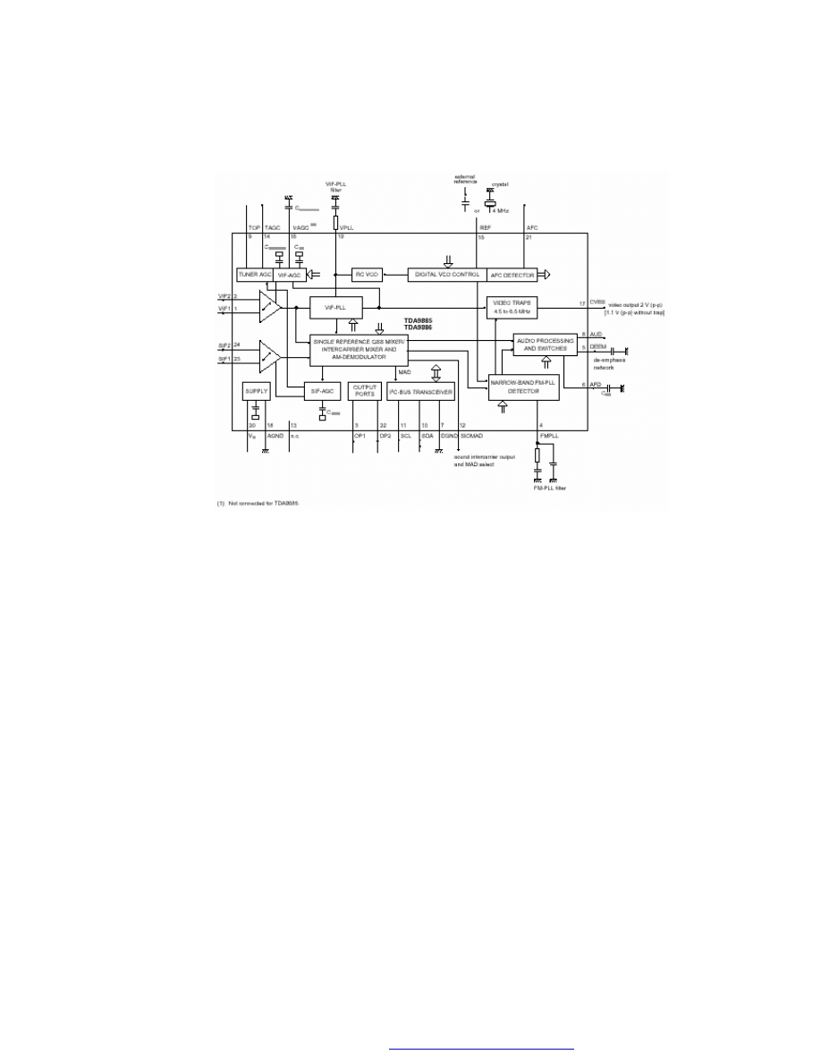
3. IF PART (TDA9886)
The TDA9886 is an alignment-free multistandard (PAL, SECAM and NTSC) vision and sound IF signal PLL
Both devices can be used for TV, VTR, PC and set-top box applications.
The following figure shows the simplified block diagram of the integrated circuit.
The integrated circuit comprises the following functional blocks:
PDF created with FinePrint pdfFactory trial version
2
Plasma TV Service Manual
24/10/2003
VIF amplifier, Tuner and VIF-AGC, VIF-AGC detector, Frequency Phase-Locked Loop (FPLL) detector, VCO
and divider, Digital acquisition help and AFC, Video demodulator and amplifier, Sound carrier trap, SIF
amplifier, SIF-AGC detector, Single reference QSS mixer, AM demodulator, FM demodulator and acquisition
help, Audio amplifier and mute time constant,
I²C
-bus transceivers and MAD (module address), Internal
voltage stabilizer.
4. MULTI STANDARD SOUND PROCESSOR
The MSP34x1G family of single-chip Multistandard Sound Processors covers the sound processing of
all analog TV-Standards worldwide, as well as the NICAM digital sound standards. The full TV sound
processing, starting with analog sound IF signal-in, down to processed analog AF-out, is performed on
a single chip.
These TV sound processing ICs include versions for processing the multichannel television sound
(MTS) signal conforming to the standard recommended by the Broadcast Television Systems
Committee (BTSC). The DBX noise reduction, or alternatively, Micronas Noise Reduction (MNR) is
performed alignment free. Other processed standards are the Japanese FM-FM multiplex standard
(EIA-J) and the FM Stereo Radio standard.
Current ICs have to perform adjustment procedures in order to achieve good stereo separation for
BTSC and EIA-J. The MSP34x1G has optimum stereo performance without any adjustments.
5. 4.VIDEO SWITCH TEA6415
In case of three or more external sources are used, the video switch IC TEA6415 is used. The main
function of this device is to switch 8 video-input sources on the 6 outputs.
Each output can be switched on only one of each input. On each input an alignment of the lowest level
of the signal is made (bottom of sync. top for CVBS or black level for RGB signals).
Each nominal gain between any input and output is 6.5dB.For D2MAC or Chroma signal the alignment
is switched off by forcing, with an external resistor bridge, 5VDC on the input. Each input can be used
as a normal input or as a MAC or Chroma input (with external Resistor Bridge). All the switching
possibilities are changed through the BUS. Driving 75ohm load needs an external resistor. It is possible
to have the same input connected to several outputs.
6. AUDIO AMPLIFIER STAGE WITH TDA7265
The TDA7265 is class AB dual Audio power amplifier assembled in the Multiwatt package, specially
designed for high quality sound application as Hi-Fi music centers and stereo TV sets.
PDF created with FinePrint pdfFactory trial version

3
Plasma TV Service Manual
24/10/2003
7. POWER SUPPLY (SMPS)
The DC voltages required at various parts of the chassis are provided by an SMPS transformer
controlled by the IC MC44608, which is designed for driving, controlling and protecting switching
transistor of SMPS. The transformer generates 145V for FBT input, +/-14V for audio amplifier, 5V and
3.3V stand by voltage and 8V, 12V and 5V supplies for other different parts of the chassis.
An optocoupler is used to control the regulation of line voltage and stand-by power consumption. There
is a regulation circuit in secondary side. This circuit produces a control voltage according to the
changes in 145V DC voltage, via an optocoupler (TCET1102G) to pin3 of the IC.
During the switch on period of the transistor, energy is stored in the transformer. During the switch off
period energy is fed to the load via secondary winding. By varying switch-on time of the power
transistor, it controls each portion of energy transferred to the second side such that the output voltage
remains nearly independent of load variations.
8. MICROCONTROLLER
The microprocessor is embedded inside PW181 chip which also handles scaling, frame rate conversion
and OSD generation. The on-chip 16-bit microprocessor is a Turbo x86-compatible processor core with
on-chip peripherals (timers, interrupt controller, 2-wire serial master/slave interface, UART, I/O ports,
and more). Special peripherals such as Infrared (IR) pulse decoders and a digital pulse width modulator
(PWM) are also included. There are two independent 2-wire serial master/slave interface modules that
can be multiplexed to control up to five 2-wire serial ports. The slave 2-wire interface is designed for
HDCP use only (and requires the use of HDCP Image Processors). On-chip RAM of up to 64 Kbytes is
available. A complete microprocessor system can be implemented simply by adding external ROM. The
on-chip processor can be disabled to allow external processor control of all internal functions.
9. SERIAL ACCESS CMOS 4K x 8 (32K bit) EEPROM 24C32A
The Microchip Technology Inc. 24C32A is a 4K x 8 (32K bit) Serial Electrically Erasable PROM. It has
been developed for advanced, low power applications such as personal communications or data
acquisition. The 24C32A also has a page-write capability of up to 32 bytes of data. The 24C32A is
capable of both random and sequential reads up to the 32K boundary. Functional address lines allow
up to eight 24C32A devices on the same bus, for up to 256K bits address space. Advanced CMOS
technology and broad voltage range make this device ideal for low-power/low-voltage, non-volatile code
and data applications.
10. CLASS AB STEREO HEADPHONE DRIVER TDA1308
The TDA1308 is an integrated class AB stereo headphone driver contained in a DIP8 plastic package.
The device is fabricated in a 1 mm CMOS process and has been primarily developed for po rtable digital
audio applications.
11. SAW FILTERS
K9656M:
Standard:
• B/G
• D/K
• I
• L/L’
Features
• TV IF audio filter with two channels
• Channel 1 (L’) with one pass band for sound carriers at 40,40 MHz (L’) and 39,75 MHz (L’- NICAM)
• Channel 2 (B/G,D/K,L,I) with one pass band for sound carriers between 32,35 MHz and 33,40 MHz
Terminals
• Tinned CuFe alloy
Pin configuration
1 Input
2 Switching input
3 Chip carrier - ground
4 Output
5 Output
PDF created with FinePrint pdfFactory trial version

4
Plasma TV Service Manual
24/10/2003
K3953M:
Standard:
• B/G
• D/K
• I
• L/L’
Features
TV IF video filter with Nyquist slopes at 33,90 MHz and 38,90 MHz
Constant group delay
Suitable for CENELEC EN 55020
Terminals
Tinned CuFe alloy
Pin configuration
1 Input
2 Input - ground
3 Chip carrier - ground
4 Output
5 Output
12. IC DESCRIPTIONS AND INTERNAL BLOCK DIAGRAM
MC44608
TCET1102G
TDA9886
TEA6415C
SAA3010T
24C32
SAA5264
LM317T
ST24LC21
TLC7733
74LVC257A
74LVC14A
TEA6420D
LM1086
LM1117
DS90C385
TL431
MSP3411G
TDA7265
TDA1308
PI5V330
AD9883A
SAA7118E
TPS72501
TSOP1836
PCF8591
PW1231
PW181
SIL151B
SDRAM 4M x 16 (MT48LC4M16A2TG-75)
FLASH
PDF created with FinePrint pdfFactory trial version
5
Plasma TV Service Manual
24/10/2003
12.1. MC44608
12.1.1. Description
The MC44608 is a high performance voltage mode controller designed for off–line converters. This high
voltage circuit that integrates the start–up current source and the oscillator capacitor, requires few
external components while offering a high flexibility and reliability. The device also features a very high
efficiency stand–by management consisting of an effective Pulsed Mode operation. This technique
enables the reduction of the stand–by power consumption to approximately 1W while delivering 300mW
in a 150W SMPS.
• Integrated Start–Up Current Source
• Fast Start–Up
• Lossless Off–Line Start–Up
• Direct Off–Line Operation
12.1.2. General Features
• Flexibility
• Duty Cycle Control
• Under voltage Lockout with Hysteresis
• On Chip Oscillator Switching Frequency 40, or 75kHz
• Secondary Control with Few External Components
Protections
• Maximum Duty Cycle Limitation
• Cycle by Cycle Current Limitation
• Demagnetization (Zero Current Detection) P rotection
• “Over V
CC
Protection” Against Open Loop
• Programmable Low Inertia Over Voltage Protection Against Open Loop
• Internal Thermal Protection
GreenLine
TM
Controller
• Pulsed Mode Techniques for a Very High Efficiency Low Power Mode
• Lossless Startup
• Low dV/dT for Low EMI Radiations
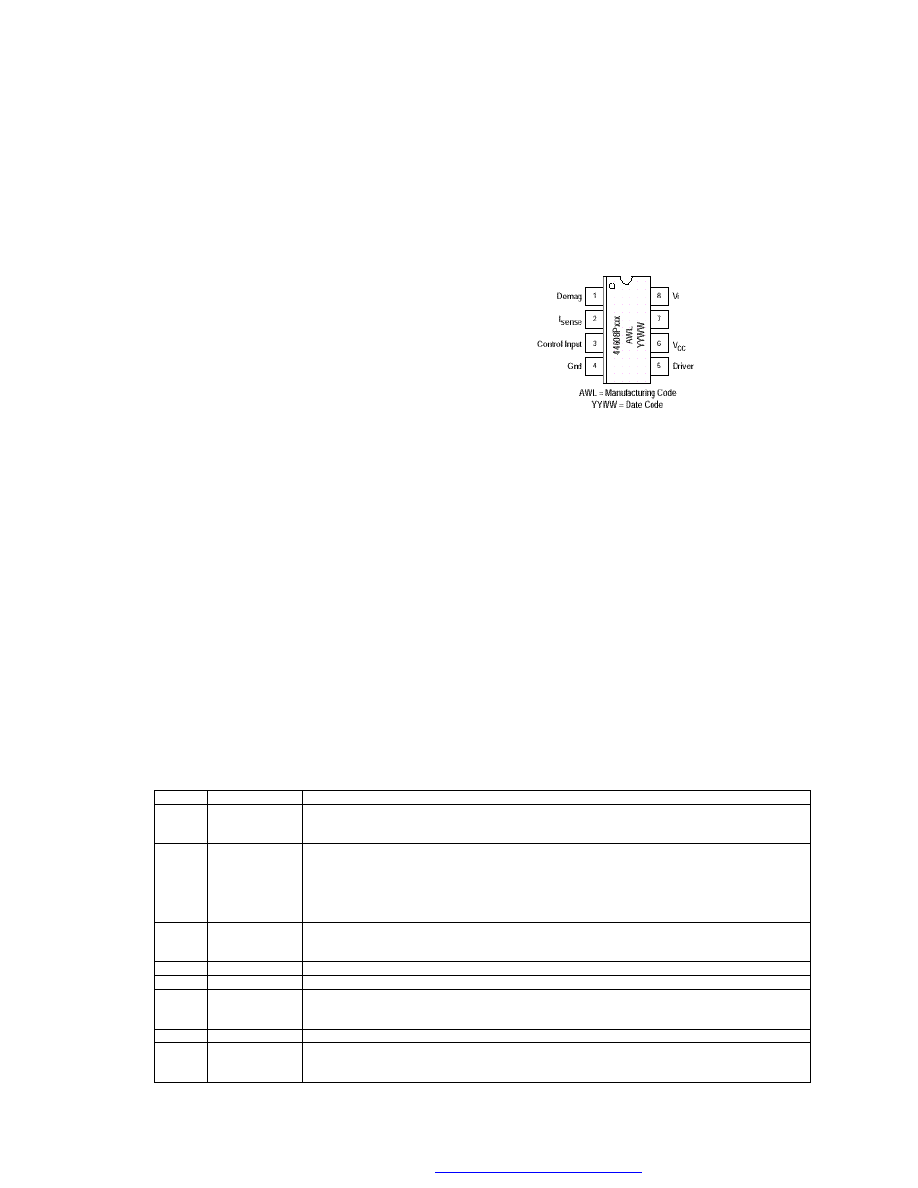
12.1.3. Pin Connections
Pin
Name
Description
1
Demag
The Demag pin offers 3 different functions: Zero voltage crossing detection (50mV), 24mA current
detection and 120mA current detection. The 24mA level is used to detect the secondary
reconfiguration status and the 120mA level to detect an Over Voltage status called Quick OVP.
2
ISENSE
The Current Sense pin senses the voltage developed on the series resistor inserted in the source
of the power MOSFET. When I sense reaches 1V, the Driver output (pin 5) is disabled. This is
known as the Over Current Protection function. A 200mA current source is flowing out of the pin 3
during the start–up phase and during the switching phase in case of the Pulsed Mode of operation.
A resistor can be inserted between the sense resistor and the pin 3; thus a programmable peak
current detection can be performed during the SMPS stand–by mode.
3
Control Input
A feedback current from the secondary side of the SMPS via the opto –coupler is injected into this
pin. A resistor can be connected between this pin and GND to allow the programming of the Burst
duty cycle during the Stand–by mode.
4
Ground
This pin is the ground of the primary side of the SMPS.
5
Driver
The current and slew rate capability of this pin are suited to drive Power MOSFETs.
6
VCC
This pin is the positive supply of the IC. The driver output gets disabled when the voltage becomes
higher than 15V and the operating range is between 6.6V and 13V. An intermediate voltage level
of 10V creates a disabling condition called Latched Off phase.
7
This pin is to provide isolation between the Vi pin 8 and the VCC pin 6.
8
Vi
This pin can be directly connected to a 500V voltage source for start –up function of the IC. During
the Start–up phase a 9 mA current source is internally delivered to the VCC pin 6 allowing a rapid
charge of the VCC capacitor. As soon as the IC starts–up, this current source is disabled.
PDF created with FinePrint pdfFactory trial version

6
Plasma TV Service Manual
24/10/2003
12.2. TCET1102G
12.2.1. Description
The TCET110/ TCET2100/ TCET4100 consists of a phototransistor optically coupled to a gallium
arsenide infrared-emitting diode in a 4-lead up to 16-lead plastic dual inline package. The elements are
mounted on one lead frame using a coplanar technique, providing a fixed distance between input and
output for highest safety requirements.
12.2.2. Applications
Circuits for safe protective separation against electrical shock according to safety class II (reinforced
isolation):
For appl. class I – IV at mains voltage
≤300 V
For appl. class I – III at mains voltage
≤600 V
According to VDE 0884, table 2, suitable for: Switch-mode power supplies, line receiver, computer
peripheral interface, microprocessor system interface.
12.2.3. 13.12.3.Features
VDE 0884 related features:
Rated impulse voltage (transient overvoltage) V
IOTM
= 8 kV peak
Isolation test voltage (partial discharge test voltage) V
pd
= 1.6 kV
Rated isolation voltage (RMS includes DC) V
IOWM
= 600 V
RMS
(848 V peak)
Rated recurring peak voltage (repetitive) V
IORM
= 600 V
RMS
General features:
CTR offered in 9 groups
Isolation materials according to UL94-VO
Pollution degree 2 (DIN/VDE 0110 / resp. IEC 664)
Climatic classification 55/100/21 (IEC 68 part 1)
Special construction: Therefore, extra low coupling capacity of typical 0.2pF, high Common Mode
Rejection
Low temperature coefficient of CTR
G = Leadform 10.16 mm; provides creepage distance > 8 mm, for TCET2100/ TCET4100 optional;
suffix letter ‘G’ is not marked on the optocoupler
Coupling System U
12.3.
TDA9886
12.3.1. General Description
The TDA9885 is an alignment-free single standard (without positive modulation) vision and sound IF signal
PLL.
12.3.2. Features
•
5 V supply voltage
•
Gain controlled wide-band Vision Intermediate Frequency (VIF) amplifier (AC-coupled)
•
Multistandard true synchronous demodulation with active carrier regeneration (very linear demodulation,
good intermodulation figures, reduced harmonics, excellent pulse response)
•
Gated phase detector for L/L accent standard
•
Fully integrated VIF Voltage Controlled Oscillator (VCO), alignment-free; frequencies switchable for all
negative and positive modulated standards via I
2
C-bus
•
Digital acquisition help, VIF frequencies of 33.4, 33.9, 38.0, 38.9, 45.75 and 58.75 MHz
•
4 MHz reference frequency input [signal from Phase-Locked Loop (PLL) tuning system] or operating as
crystal oscillator
•
VIF Automatic Gain Control (AGC) detector for gain control, operating as peak sync detector for negative
modulated signals and as a peak white detector for positive modulated signals
•
Precise fully digital Automatic Frequency Control (AFC) detector with 4-bit digital-to-analog converter; AFC
bits via I
2
C -bus readable
PDF created with FinePrint pdfFactory trial version

7
Plasma TV Service Manual
24/10/2003
•
TakeOver Point (TOP) adjustable via I
2
C-bus or alternatively with potentiometer
•
Fully integrated sound carrier trap for 4.5, 5.5, 6.0 and 6.5 MHz, controlled by FM-PLL oscillator
•
Sound IF (SIF) input for single reference Quasi Split Sound (QSS) mode (PLL controlled)
•
SIF AGC for gain controlled SIF amplifier; single reference QSS mixer able to operate in high performance
single reference QSS mode and in intercarrier mode, switchable via I
2
C-bus
•
AM demodulator without extra reference circuit
•
Alignment-free selective FM-PLL demodulator with high linearity and low noise
•
I
2
C-bus control for all functions
•
I
2
C-bus transceiver with pin programmable Module Address (MAD).
12.3.3. Pinning
SYMBOL
PIN
DESCRIPTION
VIF1
1
VIF differential input 1
VIF2
2
VIF differential input 2
OP1
3
output 1 (open-collector)
FMPLL
4
FM-PLL for loop filter
DEEM
5
de-emphasis output for capacitor
AFD
6
AF decoupling input for capacitor
DGND
7
digital ground
AUD
8
audio output
TOP
9
tuner AGC TakeOver Point (TOP)
SDA
10
I
2
C-bus data input/output
SCL
11
I
2
C-bus clock input
SIOMA
12
sound intercarrier output and MAD select
n.c.
13
not connected
TAGC
14
tuner AGC output
REF
15
4 MHz crystal or reference input
VAGC
16
VIF-AGC for capacitor; note 1
CVBS
17
video output
AGND
18
analog ground
VPLL
19
VIF-PLL for loop filter
V
P
20
supply voltage (+5 V)
AFC
21
AFC output
OP2
22
output 2 (open-collector)
SIF1
23
SIF differential input 1
SIF2
24
SIF differential input 2
12.4.
TEA6415C
12.4.1. General Description
The main function of the IC is to switch 8 video input sources on 6 outputs. Each output can be
switched on only one of each input. On each input an alignment of the lowest level of the signal is made
(bottom of synch. top for CVBS or black level for RGB signals). Each nominal gain between any input
and output is 6.5dB. For D2MAC or Chroma signal the alignment is switched off by forcing, with an
external resistor bridge, 5 V
DC
on the input. Each input can be used as a normal input or as a MAC or
Chroma input (with external resistor bridge). All the switching possibilities are changed through the
BUS. Driving 75
Ω load needs an external transistor. It is possible to have the same input connected to
several outputs. The starting configuration upon power on (power supply: 0 to 10V) is undetermined. In
this case, 6 words of 16 bits are necessary to determine one configuration. In other case, 1 word of 16
bits is necessary to determine one configuration.
12.4.2. Features
• 20MHz Bandwidth
• Cascadable with another TEA6415C (Internal address can be changed by pin 7 voltage)
• 8 Inputs (CVBS, RGB, MAC, CHROMA,...)
• 6 Outputs
PDF created with FinePrint pdfFactory trial version

8
Plasma TV Service Manual
24/10/2003
• Possibility of MAC or chroma signal for each input by switching-off the clamp with an external resistor
bridge
• Bus controlled
• 6.5dB gain between any input and output
• 55dB crosstalk at 5mHz
• Fully ESD protected
12.4.3. Pinning
1.
Input
:
Max
: 2Vpp, Input Current: 1mA, Max : 3mA
2.
Data
:
Low level
: -0.3V Max: 1.5V,
High level
: 3.0V Max
: Vcc+0.5V
3.
Input
:
Max
: 2Vpp, Input Current: 1mA,
Max
: 3mA
4.
Clock
:
Low level
: -0.3V Max: 1.5V,
High level
: 3.0V Max
: Vcc+0.5V
5.
Input
:
Max
: 2Vpp, Input Current: 1mA, Max : 3mA
6.
Input
:
Max
: 2Vpp, Input Current: 1mA, Max : 3mA
7.
Prog
8.
Input
:
Max
: 2Vpp, Input Current: 1mA, Max: 3mA
9.
Vcc
:
12V
10.
Input
:
Max
: 2Vpp, Input Current: 1mA, Max : 3mA
11.
Input
:
Max
: 2Vpp, Input Current: 1mA, Max : 3mA
12.
Ground
13.
Output :
5.5Vpp,
Min : 4.5Vpp
14.
Output :
5.5Vpp,
Min : 4.5Vpp
15.
Output :
5.5Vpp,
Min : 4.5Vpp
16.
Output :
5.5Vpp,
Min : 4.5Vpp
17.
Output :
5.5Vpp,
Min : 4.5Vpp
18.
Output :
5.5Vpp,
Min : 4.5Vpp
19.
Ground
20.
Input
:
Max : 2Vpp, Input Current
: 1mA, Max
: 3mA
12.5.
SAA3010T
12.5.1. Description
The SAA3010 is intended as a general purpose (RC-5) infrared remote control system for use where a low
voltage supply and a large debounce time are expected.
The device can generate 2048 different commands
and utilizes a keyboard with a single pole switch for each key. The commands are arranged so that 32
systems can be addressed, each system containing 64 different commands. The circuit response to legal
(one key pressed at a time) and illegal (more than one key pressed at a time) keyboard operation is specified
in the section “Keyboard operation”.
12.5.2. Features
Low voltage requirement
Biphase transmission technique
Single pin oscillator
Test mode facility
12.5.3. Pinning
Pin
Mnemonic
Function
1
X7 (IPU)
sense input from key matrix
2
SSM (I)
sense mode selection input
3
Z0-Z3 (IPU)
sense inputs from key matrix
7
MDATA (OP3)
generated output data modulated with 1/12 the oscillator frequency at a 25% duty factor
8
DATA (OP3)
generated output information
9-13
DR7-DR3 (ODN)
Scan drivers
14
VSS
Ground (0V)
15-17
DR-2-DR0 (ODN)
Scan drivers
18
OSC (I)
Oscillator input
PDF created with FinePrint pdfFactory trial version

9
Plasma TV Service Manual
24/10/2003
19
TP2 (I)
test point 2
20
TP1 (I)
Test point 1
21-27
X0-X6 (IPU)
Sense inputs from key matrix
28
VDD(I)
Voltage supply
Note:
(I): Input,
(IPU): input with p-channel pull-up transistor,
(ODN): output with open drain n-channel transistor
(OD3): output 3-state
12.6.
24C32A
12.6.1. Features
• Voltage operating range: 4.5V to 5.5V
- Maximum write current 3 mA at 5.5V
- Standby current 1 mA typical at 5.0V
• 2-wire serial interface bus, I
2
C
TM
compatible
• 100 kHz and 400 kHz compatibility
• Self-timed ERASE and WRITE cycles
• Power on/off data protection circuitry
• Hardware write protect
• 1,000,000 Erase/Write cycles guaranteed
• 32-byte page or byte write modes available
• Schmitt trigger filtered inputs for noise suppression
• Output slope control to eliminate ground bounce
• 2 ms typical write cycle time, byte or page
• Up to eight devices may be connected to the same bus for up to 256K bits total memory
• Electrostatic discharge protection > 4000V
• Data retention > 200 years
• 8-pin PDIP and SOIC packages
• Temperature ranges
- Commercial (C): 0°C to 70°C
- Industrial (I): -40°C to +85°C
- Automotive (E): -40°C to +125°C
12.6.2. Description
The Microchip Technology Inc. 24C32A is a 4K x 8 (32K bit) Serial Electrically Erasable PROM. It has
been developed for advanced, low power applications such as personal communications or data
acquisition. The 24C32A also has a page-write capability of up to 32 bytes of data. The 24C32A is
capable of both random and sequential reads up to the 32K boundary. Functional address lines allow
up to eight 24C32A devices on the same bus, for up to 256K bits address space. Advanced CMOS
technology and broad voltage range make this device ideal for low-power/low-voltage, non-volatile code
and data applications. The 24C32A is available in the standard 8-pin plastic DIP and both 150 mil and
200 mil SOIC packaging.
12.6.3. Pin Function table
Name
Function
A0, A1, A2
User Configurable Chip Selects
V
ss
Ground
SDA
Serial Address/Data I/O
SCL
Serial Clock
WP
Write Protect Input
V
cc
+4.5V to 5.5V Power Supply
PDF created with FinePrint pdfFactory trial version
10
Plasma TV Service Manual
24/10/2003
12.6.4. Functional Descriptions
The 24C32A supports a Bi-directional 2-wire bus and data transmission protocol. A device that sends
data onto the bus is defined as transmitter, and a device receiving data as receiver. The bus must be
controlled by a master device which generates the Serial Clock (SCL), controls the bus access, and
generates the START and STOP conditions, while the 24C32A works as slave. Both master and slave
can operate as transmitter or receiver but the master device determines which mode is activated.
12.7.
SAA5264
12.7.1. Features
The following features apply to both SAA5264 and SAA5265:
•
Complete 625 line teletext decoder in one chip reduces printed circuit board area and cost
•
Automatic detection of transmitted fastext links or service information (packet 8/30)
•
On-Screen Display (OSD) for user interface menus using teletext and dedicated menu icons
•
Video Programming System (VPS) decoding
•
Wide Screen Signalling (WSS) decoding
•
Pan-European, Cyrillic, Greek/Turkish and French/Arabic character sets in each chip
•
High-level command interface via I
2
C-bus gives easy control with a low software overhead
•
High-level command interface is backward compatible to Stand-Alone Fastext And Remote Interface
(SAFARI)
•
625 and 525 line display
•
RGB interface to standard colour decoder ICs, current source
•
Versatile 8-bit open-drain Input/Output (I/O) expander, 5 V tolerant
•
Single 12 MHz crystal oscillator
•
3.3 V supply voltage.
SAA5264 features
•
Automatic detection of transmitted pages to be selected by page up and page down
•
8 Page fastext decoder
•
Table Of Pages (TOP) decoder with Basic Top Table (BTT) and Additional Information Tables (AITs)
•
4 Page user-defined list mode.
12.7.2. General Description
The SAA5264 is a single-chip ten page 625-line World System Teletext decoder with a high-level
command interface, and is SAFARI compatible.
The device is designed to minimize the overall system cost, due to the high -level command interface
offering the benefit of a low software overhead in the TV microcontroller.
The SAA5264 has the following functionality:
• 10 page teletext decoder with OSD, Fastext, TOP, default and list acquisition modes
• Automatic channel installation support
• Closed caption acquisition and display
• Violence Chip (VChip) support.
12.7.3. Pin Connections and Short Descriptions
SYMBOL
PIN
TYPE
DESCRIPTION
Port 2: 8-bit programmable bidirectional port with alternative functions
P2.0/PWM
1
I/O
output for 14-bit high precision Pulse Width Modulator (PWM)
P2.1/PWM0
2
I/O
outputs for 6-bit PWMs 0 to 6
P2.2/PWM1
3
I/O
P2.3/PWM2
4
I/O
P2.4/PWM3
5
I/O
P2.5/PWM4
6
I/O
P2.6/PWM5
7
I/O
P2.7/PWM6
8
I/O
Port 3: 8-bit programmable bidirectional port with alternative functions
P3.0/ADC0
9
I/O
inputs for the software Analog-to-Digital-Converter (ADC) facility
P3.1/ADC1
10
I/O
PDF created with FinePrint pdfFactory trial version

11
Plasma TV Service Manual
24/10/2003
P3.2/ADC2
11
I/O
P3.3/ADC3
12
I/O
P3.4/PWM7
30
I/O
output for 6-bit PWM7
V
SSC
13
I/O
core ground
Port 0: 8-bit programmable bidirectional port
SCL(NVRAM)
14
I
I
2
C-bus Serial Clock input to Non-Volatile RAM
SDA(NVRAM)
15
I/O
I
2
C-bus Serial Data input/output (Non-Volatile RAM)
P0.2
16
I/O
input/output for general use
P0.3
17
I/O
input/output for general use
P0.4
18
I/O
input/output for general use
P0.5
19
I/O
8 mA current sinking capability for direct drive of Light Emitting
Diodes (LEDs)
P0.6
20
I/O
P0.7
21
I/O
input/output for general use
V
SSA
22
-
analog ground
CVBS0
23
I
Composite Video Baseband Signal (CVBS) input; a positive-going
1V
CVBS1
24
I
(peak-to-peak) input is required; connected via a 100 nF capacitor
SYNC_FILTER
25
I
sync-pulse-filter input for CVBS; this pin should be connected to
V
SSA
via a 100 nF capacitor
IREF
26
I
reference current input for analog circuits; for correct operation a 24
κΩ
resistor should be connected to
V
SSA
FRAME
27
O
Frame de-interlace output synchronized with the VSYNC pulse to
produce a non-interlaced display by adjustment of the vertical
deflection circuits
TEST
28
I
not available; connect this pin to
V
SSA
COR
29
O
contrast reduction: open-drain, active LOW output which allows
selective contrast reduction of the TV picture to enhance a mixed
mode display
30
I/O
P3.4/PWM7 (described above)
V
DDA
31
-
analog supply voltage (3.3 V)
B
32
O
Blue colour information pixel rate output
G
33
O
Green colour information pixel rate output
R
34
O
Red colour information pixel rate output
VDS
35
O
video/data switch push-pull output for pixel rate fast blanking
HSYNC
36
I
horizontal sync pulse input: Schmitt triggered for a Transistor
Transistor Level (TTL) version; the polarity of this pulse is
programmable by register bit TXT1.H POLARITY
VSYNC
37
I
vertical sync pulse input; Schmitt triggered for a TTL version; the
polarity of this pulse is programmable by register bit TXT1.V
POLARITY
V
SSP
38
-
periphery ground
V
DDC
39
-
core supply voltage (+3.3 V)
OSCGND
40
-*
crystal oscillator ground
XTALIN
41
I
12 MHz crystal oscillator input
XTALOUT
42
O
12 MHz crystal oscillator output
RESET
43
I
reset input; if this pin is HIGH for at least 2 machine cycles (24
oscillator periods) while the oscillator is running, the device resets;
this pin should be connected to
V
DDP
via a capacitor
V
DDP
44
-
periphery supply voltage (+3.3 V)
Port 1: 8-bit programmable bidirectional port
P1.0
45
I/O
input/output for general use
P1.1
46
I/O
input/output for general use
P1.2
47
I/O
input/output for general use
P1.3
48
I/O
input/output for general use
SCL
49
I
I
2
C-bus Serial Clock input from application
PDF created with FinePrint pdfFactory trial version

12
Plasma TV Service Manual
24/10/2003
SDA
50
I/O
I
2
C-bus Serial Data input from (application)
P1.4
51
I/O
input/output for general use
P1.5
52
I/O
input/output for general use
12.8.
LM317
12.8.1. General Description
The LM117/LM217/LM317 are monolithic integrated circuit in TO-220, ISOWATT220, TO-3 and D
2
PAK packages intended for use as positive adjustable voltage regulators.
They are designed to supply more than 1.5A of load current with an output voltage adjustable over a
1.2 to 37V range.
The nominal output voltage is selected by means of only a resistive divider, making the device
exceptionally easy to use and eliminating the stocking of many fixed regulators.
12.8.2. Features
• Output voltage range : 1.2 To 37V
• Output current In excess of 1.5A
• 0.1% Line and Load Regulation
• Floating Operation for High Voltages
• Complete Series of Protections : Current Limiting, Thermal Shutdown And Soa Control
12.9.
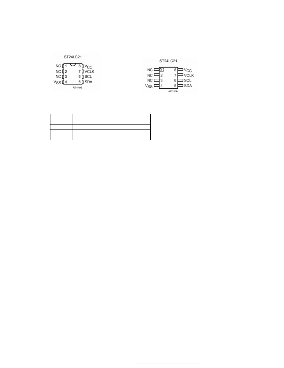
ST24LC21
12.9.1. Description
The ST24LC21 is a 1K bit electrically erasable programmable memory (EEPROM), organized by 8 bits.
This device can operate in two modes: Transmit Only mode and I
2
C bidirectional mode. When powered,
the device is in Transmit Only mode with EEPROM data clocked out from the rising edge of the signal
applied on VCLK. The device will switch to the I
2
C bidirectional mode upon the falling edge of the signal
applied on SCL pin. The ST24LC21 can not switch from the I
2
C bidirectional mode to the Transmit Only
mode (except when the power supply is removed). The device operates with a power supply value as
low as 2.5V. Both Plastic Dual-in-Line and Plastic Small Outline packages are available.
12.9.2. Features
• 1 million Erase/Write cycles
• 40 years data retention
• 2.5V To 5.5V single supply voltage
• 400k Hz compatibility over the full range of supply voltage
• Two wire serial interface I
2
C bus compatible
• Page Write (Up To 8 Bytes)
• Byte, random and sequential read modes
• Self timed programming cycle
• Automatic address incrementing
• Enhanced ESD/Latch up
• Performances
PDF created with FinePrint pdfFactory trial version
13
Plasma TV Service Manual
24/10/2003
12.9.3. Pin connections
DIP Pin connections
CO Pin connections
NC: Not connected
Signal names
SDA
Serial data Address Input/Output
SCL
Serial Clock (I
2
C mode)
V
cc
Supply voltage
V
ss
Ground
VCLK
Clock transmit only mode
12.10.
TLC7733
12.10.1. Description
The TLC77xx family of micropower supply voltage supervisors are designed for reset control, primarily
in microcomputer and microprocessor systems.
During power-on, RESET is asserted when V
DD
reaches 1 V. After minimum V
DD
(.
2 V) is established,
the circuit monitors SENSE voltage and keeps the reset outputs active as long as SENSE voltage
(V
I(SENSE)
)
remains below the threshold voltage. An internal timer delays return of the output to the inactive state to
ensure proper system reset. The delay time, t
d
, is determined by an external capacitor:
t
d
= 2.1 x 10
4
x C
T
where
C
T
is in farads
t
d
is in seconds
The TLC77xx has a fixed SENSE threshold voltage set by an internal voltage divider. When SENSE
voltage drops below the threshold voltage, the outputs become active and stay in that state until
SENSE voltage returns above threshold voltage and the delay time, t
d
, has expired.
In addition to the power-on-reset and undervoltage-supervisor function, the TLC77xx adds power-down
control support for static RAM. When CONTROL is tied to GND, RESET will act as active high. The
voltage monitor contains additional logic intended for control of static memories with battery backup
during power failure. By driving the chip select (CS) of the memory circuit with the RESET output of the
TLC77xx and with the CONTROL driven by the memory bank select signal (CSH1) of the
microprocessor (see Figure 10), the memory circuit is automatically disabled during a power loss. (In
this application the TLC77 xx power has to be supplied by the battery.)
The TLC77xxQ is characterized for operation over a temperature range of –4
0°
C to 125
°
C, and the
TLC77xxI is characterized for operation over a temperature range of –40
°
C to 85
°
C.
PDF created with FinePrint pdfFactory trial version

14
Plasma TV Service Manual
24/10/2003
12.11.
74LVC257A
12.11.1. Features
Wide supply voltage range of 1.2 to 3.6 V
In accordance with JEDEC standard no. 8-1A
CMOS lower power consumption
Direct interface with TTL levels
Output drive capability 50 _ transmission lines at 85°C
5 Volt tolerant inputs/outputs, for interfacing with 5 Volt logic
12.11.2. Description
The 74LVC257A is a high-performance, low-power, low-voltage, Si-gate CMOS device and superior to
most advanced CMOS compatible TTL families.
Inputs can be driven from either 3.3V or 5.0V devices. In 3-State operation, outputs can handle 5V. This
feature allows the use of these devices as translators in a mixed 3.3V/5V environment.
The 74LVC257A is a quad 2-input multiplexer with 3-state outputs, which select 4 bits of data from two
sources and are controlled by a common data select input (S). The data inputs from source 0 (1l 0 to 4l
0 ) are selected when input S is LOW and the data inputs from source 1 (1l 1 to 4l 1 ) are selected
when S in HIGH. Data appears at the outputs (1Y to 4Y) in true (non-inverting) form from the selected
inputs. The 74LVC257A is the logic implementation of a 4-pole, 2-position switch, where the position of
the switch is determined by the logic levels applied to S. The outputs are forced to a high impedance
OFF-state when OE is HIGH.
12.11.3. Pin Description
PIN NUMBER
SYMBOL
DESCRIPTION
1
S
Common data select input
2, 5, 11, 14
1|
0
to 4|
0
Data inputs from source 0
3, 6, 10, 13
1|
1
to 4|
1
Data outputs from source 1
4,7,9,12
1Y to 4Y
3-State multiplexer outputs
8
GND
Ground (0V)
15
OE
3-State output enable input (active LOW)
16
V
cc
Positive supply voltage
12.12.
74LVC14A
12.12.1. Features
• Wide supply voltage range of 1.2 to 3.6 V
• In accordance with JEDEC standard no. 8-1A
• Inputs accept voltages up to 5.5 V
• CMOS low power consumption
• Direct interface with TTL levels
12.12.2. Applications
• Wave and pulse shapers for highly noisy environments
• Astable multivibrators
• Monostable multivibrators
12.12.3. Description
The 74LVC14A is a high-performance, low power, low-voltage Si-gate CMOS device and superior to
most advanced CMOS compatible TTL families.
Inputs can be driven from either 3.3 V or 5 V devices. This feature allows the use of these devices as
translators in a mixed 3.3 V/5 V environment.
The 74LVC14A provides six inverting buffers with Schmitt-trigger action. It is capable of transforming
slowly changing input signals into sharply defined, jitter -free output signals.
PDF created with FinePrint pdfFactory trial version
15
Plasma TV Service Manual
24/10/2003
12.12.4. Pin Description
PIN NUMBER
SYMBOL
DESCRIPTION
1, 3, 5, 9, 11, 13
1A – 6A
Data inputs
2, 4, 6, 8, 10, 12
1Y – 6Y
Data outputs
7
GND
Ground (0V)
14
V
cc
Positive supply voltage
12.13.
TEA6420
12.13.1. Features
• 5 Stereo Inputs
• 4 Stereo Ouputs
• Gain Control 0/2/4/6db/Mutefor EachOutput
• Cascadable (2 Different Addresses)
• Serial Bus Controlled
• Very Low noise
• Very Low distorsion
12.13.2. Description
The TEA6420 switches 5 stereo audio inputs on 4 stereo outputs.
All the switching possibilities are changed through the I
2
C bus.
12.14.
LM1086
12.14.1. Description
The LM1086 is a series of low dropout positive voltage regulators with a maximum dropout of 1.5V at
1.5A of load current. It has the same pin-out as National Semiconductor’s industry standard LM317.
The LM1086 is available in an adjustable version, which can set the output voltage with only two
external resistors. It is also available in five fixed voltages: 2.5V, 2.85V, 3.3V, 3.45V and 5.0V. The fixed
versions integrate the adjust resistors. The LM1086 circuit includes a zener trimmed band-gap
reference, current limiting and thermal shutdown.
12.14.2. Features
• Available in 2.5V, 2.85V, 3.3V, 3.45V, 5V and Adjustable Versions
• Current Limiting and Thermal Protection
• Output Current 1.5A
• Line Regulation 0.015% (typical)
• Load Regulation 0.1% (typical)
PDF created with FinePrint pdfFactory trial version
16
Plasma TV Service Manual
24/10/2003
12.14.3. Applications
• SCSI-2 Active Terminator
• High Efficiency Linear Regulators
• Battery Charger
• Post Regulation for Switching Supplies
• Constant Current Regulator
• Microprocessor Supply
12.14.4. Connection Diagrams
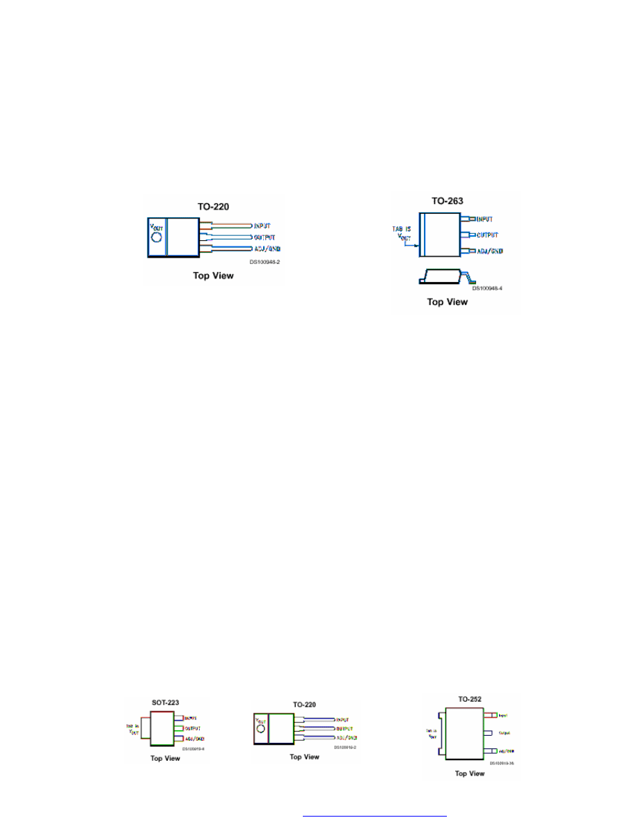
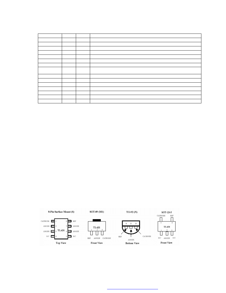
12.15. LM1117
12.15.1. General Description
The LM1117 is a series of low dropout voltage regulators with a dropout of 1.2V at 800mA of load
current. It has the same pin-out as National Semiconductor’s industry standard LM317. The LM1117 is
available in an adjustable version, which can set the output voltage from 1.25V to 13.8V with only two
external resistors. In addition, it is also available in five fixed voltages, 1.8V, 2.5V, 2.85V, 3.3V, and 5V.
The LM1117 offers current limiting and thermal shutdown. Its circuit includes a zener trimmed bandgap
reference to as-sure output voltage accuracy to within ±1%. The LM1117 series is available in SOT-
223, TO-220, and TO-252 D-PAK packages. A minimum of 10µF tantalum capacitor is required at the
output to improve the transient response and stability.
12.15.2. Features
• Available in 1.8V, 2.5V, 2.85V, 3.3V, 5V, and Adjustable Versions
• Space Saving SOT-223 Package
• Current Limiting and Thermal Protection
• Output Current 800mA
• Line Regulation 0.2% (Max)
• Load Regulation 0.4% (Max)
• Temperature Range
— LM1117 0°C to 125°C
— LM1117I -40°C to 125°C
12.15.3. Applications
• 2.85V Model for SCSI-2 Active Termination
• Post Regulator for Switching DC/DC Converter
• High Efficiency Linear Regulators
• Battery Charger
• Battery Powered Instrumentation
12.15.4. Connection Diagrams
PDF created with FinePrint pdfFactory trial version

17
Plasma TV Service Manual
24/10/2003
12.16. DS90C385
12.16.1. General Description
The DS90C385 transmitter converts 28 bits of LVCMOS/LVTTL data into four LVDS (Low Voltage
Differential Signaling) data streams. A phase-locked transmit clock is transmitted in parallel with the
data streams over a fifth LVDS link.
Every cycle of the transmit clock 28 bits of input data are sampled and transmitted. At a transmit clock
frequency of 85 MHz, 24 bits of RGB data and 3 bits of LCD timing and control data (FPLINE,
FPFRAME, DRDY) are transmitted at a rate of 595 Mbps per LVDS data channel. Using an 85 MHz
clock, the data throughput is 297.5 Mbytes/sec. Also available is the DS90C365 that converts 21 bits of
LVCMOS/LVTTL data into three LVDS (Low Voltage Differential Signaling) data streams. Both
transmitters can be programmed for Rising edge strobe or falling edge strobe through a dedicated pin.
A Rising edge or Falling edge strobe transmitter will interoperate with a Falling edge strobe Receiver
(DS90CF386/DS90CF366) without any translation logic.
The DS90C385 is also offered in a 64 ball, 0.8mm fine pitch ball grid array (FBGA) package which
provides a 44 % reduction in PCB footprint compared to the TSSOP package. This chipset is an ideal
means to solve EMI and cable size problems associated with wide, high -speed TTL interfaces.
12.16.2. Features
• 20 to 85 MHz shift clock support
• Best–in–Class Set & Hold Times on TxINPUTs
• Tx power consumption <130 mW (typ) @85MHz Grayscale
• Tx Power-down mode <200µW (max)
• Supports VGA, SVGA, XGA and Dual Pixel SXGA.
• Narrow bus reduces cable size and cost
• Up to 2.38 Gbps throughput
• Up to 297.5 Megabytes/sec bandwidth
• 345 mV (typ) swing LVDS devices for low EMI
• PLL requires no external components
• Compatible with TIA/EIA-644 LVDS standard
• Low profile 56-lead or 48-lead TSSOP package
• DS90C385 also available in a 64 ball, 0.8mm fine pitch ball grid array (FBGA) package
12.16.3. Pin Description
DS90C385 MTD56 (TSSOP) Package Pin Description-FPD Link Transmitter
Pin Name
I/O
No.
Description
TxIN
I
28
TTL level input. This includes: 8 Red, 8 Green, 8 Blue, and 4 control lines —FPLINE,
FPFRAME and DRDY (also referred to as HSYNC, VSYNC, Data Enable).
TxOUT+
O
4
Positive LVDS differentiaI data output.
TxOUT-
O
4
Negative LVDS differential data output.
TxCLKIN
I
1
TTL Ievel clock input. Pin name TxCLK IN.
R_FB
I
1
Programmable strobe select
TxCLK OUT+
O
1
Positive LVDS differential clock output.
TxCLK OUT-
O
1
Negative LVDS differential clock output.
PWR DOWN
I
1
TTL level input. Assertion (low input) TRI-STATES the outputs, ensuring low current at
power down.
Vcc
I
3
Power supply pins for TTL inputs.
GND
I
4
Ground pins for TTL inputs.
PLL Vcc
I
1
Power supply pin for PLL.
PLL GND
I
2
Ground pins for PLL.
LVDS Vcc
I
1
Power supply pin for LVDS outputs.
LVDS GND
I
3
Ground pins for LVDS outputs.
PDF created with FinePrint pdfFactory trial version
18
Plasma TV Service Manual
24/10/2003
DS90C385SLC SLC64A Package Pin Description-FPD Link Transmitter
Pin Name
I/O
No.
Description
TxIN
I
28
TTL level input.
TxOUT+
O
4
Positive LVDS differentiaI data output.
TxOUT-
O
4
Negative LVDS differential data output.
TxCLKIN
I
1
TTL Ievel clock input. The rising edge acts as data strobe. Pin name TxCLK IN.
R_FB
I
1
Programmable strobe select. HIGH = rising edge, LOW = falling edge.
TxCLK OUT+
O
1
Positive LVDS differential clock output.
TxCLK OUT-
O
1
Negative LVDS differential clock output.
PWR DOWN
I
1
TTL level input. Assertion (low input) TRI-STATES the outputs, ensuring low
current at power down.
Vcc
I
3
Power supply pins for TTL inputs.
GND
I
5
Ground pins for TTL inputs.
PLL Vcc
I
1
Power supply pin for PLL.
PLL GND
I
2
Ground pins for PLL.
LVDS Vcc
I
2
Power supply pin for LVDS outputs.
LVDS GND
I
4
Ground pins for LVDS outputs.
NC
6
Pins not connected.
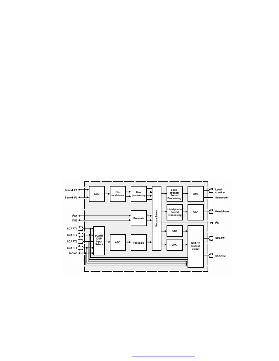
12.17. TL431
12.17.1. Description
The TL431 is a 3-terminal adjustable shunt voltage regulator providing a highly accurate 1 % band gap
reference. TL431 acts as an open-loop error amplifier with a 2.5V temperature compensation reference.
The TL431 thermal stability, wide operating current (150mA) and temperature range (0.to 105.makes it
suitable for all variety of application that are looking for a low cost solution with high performance. The
output voltage may be adjusted to any value between VREF and 36 volts with two external resistors.
The TL431 is operating in full industrial temperature range of 0°C to 105°C. The TL431 is available in
TO-92, SO-8, SOT-89 and SOT23-5 packages.
12.17.2. Features
• Trimmed Band gap to 1%
• Wide Operating Current
1mA to 150mA
• Extended Temperature Range
0. °C to 105.°C
• Low Temperature Coefficient
30 ppm /°C
• Offered in TO-92, SOIC, SOT-89, SOT-23-5
• Improved Replacement in Performance for TL431
• Low Cost Solution
12.17.3. Pin Configurations
PDF created with FinePrint pdfFactory trial version
19
Plasma TV Service Manual
24/10/2003
12.18. MSP34X1G
MSP3411G
Multistandard Sound Processor Family
12.18.1. Introduction
The MSP 34x1G family of single-chip Multistandard Sound Processors covers the sound processing of
all analog TV-Standards worldwide, as well as the NICAM digital sound standards. The full TV sound
processing, starting with analog sound IF signal-in, down to processed analog AF-out, is performed on
a single chip. Figure shows a simplified functional block diagram of the MSP 34x1G.
The MSP 34x1G has all functions of the MSP 34x0G with the addition of a virtual surround sound
feature.
Surround sound can be reproduced to a certain extent with two loudspeakers. The MSP 34x1G
includes the Micronas virtualizer algorithm “3D-PANORAMA” which has been approved by the Dolby
1)
Laboratories for with the "Virtual Dolby Surround" technology. In addition, the MSP 34x1G includes the
“PAN-ORAMA” algorithm.
These TV sound processing ICs include versions for processing the multichannel television sound
(MTS) signal conforming to the standard recommended by the Broadcast Television Systems
Committee (BTSC). The DBX noise reduction, or alternatively, Micronas Noise Reduction (MNR) is
performed alignment free.
Other processed standards are the Japanese FM-FM multiplex standard (EIA-J) and the FM Stereo
Radio standard.
Current ICs have to perform adjustment procedures in order to achieve good stereo separation for
BTSC and EIA-J. The MSP 34x1G has optimum stereo performance without any adjustments.
The MSP 34x1G has built-in automatic functions: The IC is able to detect the actual sound standard
automat-ically (Automatic Standard Detection). Furthermore, pilot levels and identification signals can
be evaluated internally with subsequent switching between mono/stereo/bilingual; no I
2
C interaction is
necessary (Automatic Sound Selection).
Source Select
I
2
S bus interface consists of five pins:
1. I
2
S_DA_IN1, I2S_DA_IN2: For input, four channels (two channels per line, 2*16 bits) per sampling
cycle (32 kHz) are transmitted.
2. I
2
S _DA_OUT: For output, two channels (2*16 bits) per sampling cycle (32 kHz) are transmitted.
3. I
2
S _CL: Gives the timing for the transmission of I
2
S serial data (1.024 MHz).
4. I
2
S _WS: The I
2
S _WS word strobe line defines the left and right sample.
PDF created with FinePrint pdfFactory trial version
20
Plasma TV Service Manual
24/10/2003
12.18.2. Features
• 3D-PANORAMA virtualizer (approved by Dolby Laboratories) with noise generator
• PANORAMA virtualizer algorithm
• Standard Selection with single I
2
C transmission
• Automatic Sound Selection (mono/stereo/bilingual),
• Automatic Carrier Mute function
• Interrupt output programmable (indicating status change)
• Loudspeaker / Headphone channel with volume, balance, bass, treble, loudness
• AVC: Automatic Volume Correction
• Subwoofer output with programmable low-pass and complementary high-pass filter
• 5-band graphic equalizer for loudspeaker channel
• Spatial effect for loudspeaker channel, processing of all deemphasis filtering
• Two selectable sound IF (SIF) inputs
• Four Stereo SCART (line) inputs, one Mono input; two Stereo SCART outputs
• Complete SCART in/out switching matrix
• Two I
2
S inputs; one I
2
S output
• Automatic Standard Detection of terrestrial TV standards
• Demodulation of the BTSC multiplex signal and the SAP channel
• Alignment free digital DBX noise reduction
• BTSC stereo separation (MSP 3441G also EIA-J) significantly better than specification
• SAP and stereo detection for BTSC system
• Demodulation of the FM-Radio multiplex signal
12.18.3. Pin connections
NC = not connected; leave vacant
LV = if not used, leave vacant
OBL = obligatory; connect as described in circuit diagram
DVSS: if not used, connect to DVSS
AHVSS: connect to AHVSS
Pin No.
Pin Name
Type
Connection
(if not used)
Short Description
PLCC
68-pin
PSDIP
64-pin
PSDIP
52-pin
PQFP
80-pin
PLQFP
64-pin
1
16
14
9
8
ADR_WS
OUT
LV
ADR word strobe
2
-
-
-
-
NC
LV
Not connected
3
15
13
8
7
ADR_DA
OUT
LV
ADR Data Output
4
14
12
7
6
I2S_DA_IN1
IN
LV
I
2
S1 data input
5
13
11
6
5
I2S_DA_OUT
OUT
LV
I
2
S data output
6
12
10
5
4
I2S_WS
IN/OUT
LV
I
2
S word strobe
7
11
9
4
3
I2S_CL
IN/OUT
LV
I
2
S clock
8
10
8
3
2
I2C_DA
IN/OUT
OBL
I
2
C data
9
9
7
2
1
I2C_CL
IN/OUT
OBL
I
2
C clock
10
8
-
1
64
NC
LV
Not connected
11
7
6
80
63
STANDBYQ
IN
OBL
Stand-by (low-active)
12
6
5
79
62
ADR_SEL
IN
OBL
I
2
C bus address select
13
5
4
78
61
D_CTR_I/O_0
IN/OUT
LV
D_CTR_I/O_0
14
4
3
77
60
D_CTR_I/O_1
IN/OUT
LV
D_CTR_I/O_1
15
3
-
76
59
NC
LV
Not connected
16
2
-
75
58
NC
LV
Not connected
17
-
-
-
-
NC
LV
Not connected
18
1
2
74
57
AUD_CL_OUT
OUT
LV
Audio clock output
(18.432 MHz)
19
64
1
73
56
TP
LV
Test pin
20
63
52
72
55
XTAL_OUT
OUT
OBL
Crystal oscillator
21
62
51
71
54
XTAL_IN
IN
OBL
Crystal oscillator
22
61
50
70
53
TESTEN
IN
OBL
Test pin
23
60
49
69
52
ANA_IN2+
IN
AVSS via
56 pF/LV
IF Input 2 (can be left
vacant, only if IF input 1 is
also not in use)
24
59
48
68
51
ANA_IN-
IN
AVSS via
56 pF/LV
IF common (can be left
vacant, only if IF input 1 is
also not in use)
25
58
47
67
50
ANA_IN1+
IN
LV
IF input 1
PDF created with FinePrint pdfFactory trial version
21
Plasma TV Service Manual
24/10/2003
26
57
46
66
49
AVSUP
OBL
Analog power supply 5V
-
-
-
65
-
AVSUP
OBL
Analog power supply 5V
-
-
-
64
-
NC
LV
Not connected
-
-
-
63
-
NC
LV
Not connected
27
56
45
62
48
AVSS
OBL
Analog ground
-
-
-
61
-
AVSS
OBL
Analog ground
28
55
44
60
47
MONO_IN
IN
LV
Mono input
-
-
-
59
-
NC
LV
Not connected
29
54
43
58
46
VREFTOP
OBL
Reference voltage IF A/D
converter
30
53
42
57
45
SC1_IN_R
IN
LV
SCART 1 input, right
31
52
41
56
44
SC1_IN_L
IN
LV
SCART 1 input, left
32
51
-
55
43
ASG1
AHVSS
Analog Shield Ground 1
33
50
40
54
42
SC2_IN_R
IN
LV
SCART 2 input, right
34
49
39
53
41
SC2_IN_L
IN
LV
SCART 2 input, left
35
48
-
52
40
ASG2
AHVSS
Analog Shield Ground 2
36
47
38
51
39
SC3_IN_R
IN
LV
SCART 3 input, right
37
46
37
50
38
SC3_IN_L
IN
LV
SCART 3 input, left
38
45
-
49
37
ASG4
AHVSS
Analog Shield Ground 4
39
44
-
48
36
SC4_IN_R
IN
LV
SCART 4 input, right
40
43
-
47
35
SC4_IN_L
IN
LV
SCART 4 input, left
41
-
-
46
-
NC
LV or AHVSS
Not connected
42
42
36
45
34
AGNDC
OBL
Analog reference voltage
43
41
35
44
33
AHVSS
OBL
Analog ground
-
-
-
43
-
AHVSS
OBL
Analog ground
-
-
-
42
-
NC
LV
Not connected
-
-
-
41
-
NC
LV
Not connected
44
40
34
40
32
CAPL_M
OBL
Volume capacitor MAIN
45
39
33
39
31
AHVSUP
OBL
Analog power supply 8V
46
38
32
38
30
CAPL_A
OBL
Volume capacitor AUX
47
37
31
37
29
SC1_OUT_L
OUT
LV
SCART output 1, left
48
36
30
36
28
SC1_OUT_R
OUT
LV
SCART output 1, right
49
35
29
35
27
VREF1
OBL
Reference ground 1
50
34
28
34
26
SC2_OUT_L
OUT
LV
SCART output 2, left
51
33
27
33
25
SC2_OUT_R
OUT
LV
SCART output 2, right
52
-
-
32
-
NC
LV
Not connected
53
32
-
31
24
NC
LV
Not connected
54
31
26
30
23
DACM_SUB
OUT
LV
Subwoofer output
55
30
-
29
22
NC
LV
Not connected
56
29
25
28
21
DACM_L
OUT
LV
Loudspeaker out, left
57
28
24
27
20
DACM_R
OUT
LV
Loudspeaker out, right
58
27
23
26
19
VREF2
OBL
Reference ground 2
59
26
22
25
18
DACA_L
OUT
LV
Headphone out, left
60
25
21
24
17
DACA_R
OUT
LV
Headphone out, right
-
-
-
23
-
NC
LV
Not connected
-
-
-
22
-
NC
LV
Not connected
61
24
20
21
16
RESETQ
IN
OBL
Power-on-reset
62
23
-
20
15
NC
LV
Not connected
63
22
-
19
14
NC
LV
Not connected
64
21
19
18
13
NC
LV
Not connected
65
20
18
17
12
I2S_DA_IN2
IN
LV
I
2
S2-data input
66
19
17
16
11
DVSS
OBL
Digital ground
-
-
-
15
-
DVSS
OBL
Digital ground
-
-
-
14
-
DVSS
OBL
Digital ground
67
18
16
13
10
DVSUP
OBL
Digital power supply 5V
-
-
-
12
-
DVSUP
OBL
Digital power supply 5V
-
-
-
11
-
DVSUP
OBL
Digital power supply 5V
68
17
15
10
9
ADR_CL
OUT
LV
ADR clock
PDF created with FinePrint pdfFactory trial version
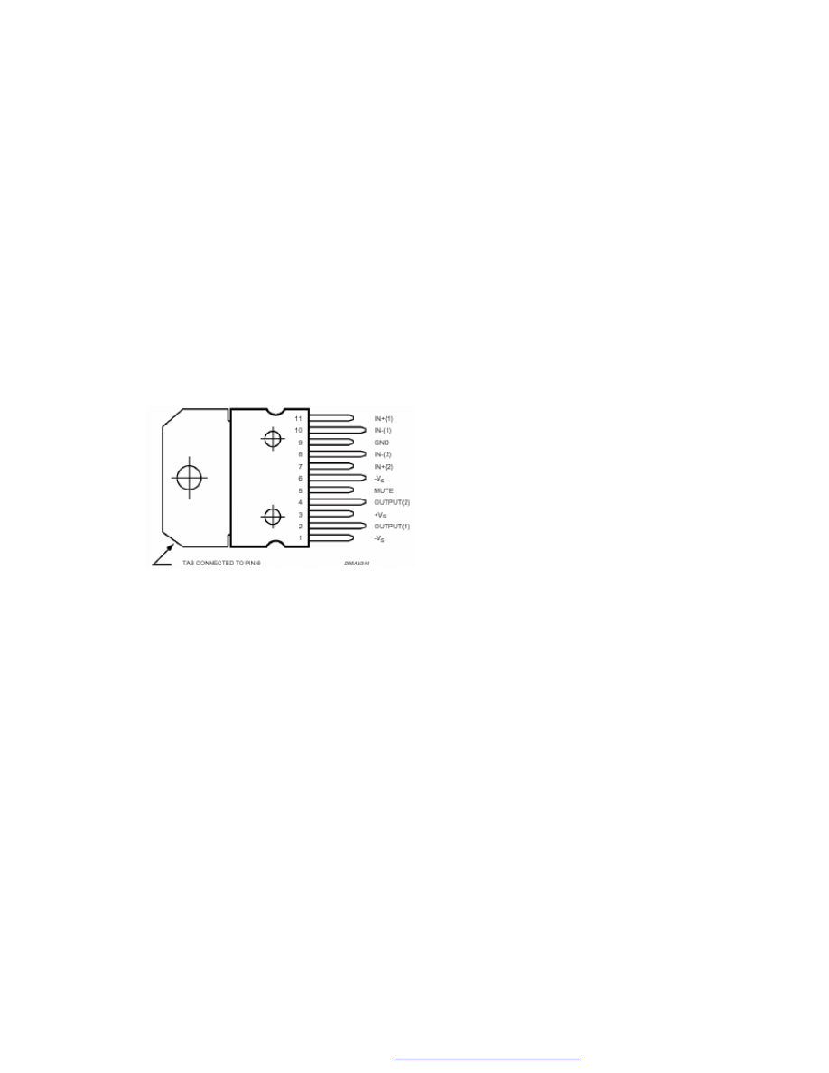
22
Plasma TV Service Manual
24/10/2003
12.19. TDA7265
12.19.1. Description
The TDA7265 is class AB dual Audio power amplifier assembled in the Multiwatt package, specially
designed for high quality sound application as Hi-Fi music centers and stereo TV sets.
12.19.2. Features
• Wide Supply Voltage Range (Up to±25V ABS Max.)
• Split Supply
• High Output Power
• 25 + 25W @THD =10%,
RL
=
8
W,
V
S= +20V
• No Popat Turn-On/Off
• Mute (Pop Free)
• Stand-By Feature (Low
I
q)
• Short Circuit Protection
• Thermal Overload Protection
12.19.3. Pin Connection
12.20. TDA1308
12.20.1. General Description
The TDA1308 is an integrated class AB stereo headphone driver contained in an SO8 or a DIP8 plastic
package. The device is fabricated in a 1 mm CMOS process and has been primarily developed for
portable digital audio applications. It gets its input from two analog audio outputs (DACA_L and
DACA_R) of MSP 34x0G. The gain of the output is adjustable by the feedback resistor between the
inputs and outputs.
12.20.2. Features
•
Wide temperature range
•
No switch ON/OFF clicks
•
Excellent power supply ripple rejection
•
Low power consumption
•
Short-circuit resistant
•
High performance
•
high signal-to-noise ratio
•
High slew rate
•
Low distortion
•
Large output voltage swing.
PDF created with FinePrint pdfFactory trial version

23
Plasma TV Service Manual
24/10/2003
12.20.3. Pinning
SYMBOL
PIN
DESCRIPTION
OUTA
1
Output A
INA(neg)
2
Inverting input A
INA(pos)
3
Non-inverting input A
V
SS
4
Negative supply
INB(pos)
5
Non-inverting input B
INB(neg)
6
Inverting input B
OUTB
7
Output B
V
DD
8
Positive supply
12.21. PI5V330
12.21.1. General Description
The PI5V330 is well suited for video applications when switching composite or RGB analog. A picture-
in-picture application will be described in this br ief. The pixel-rate creates video overlays so two or more
pictures can be viewed at the same time. An inexpensive NTSC titler can be implemented by
superimposing the output of a character generator on a standard composite video background.
12.22. AD9883A
12.22.1. General Description
The AD9883A is a complete 8-bit, 140 MSPS, monolithic analog interface optimized for capturing RGB
graphics signals from personal computers and workstations. Its 140 MSPS encode rate capability and
full power analog bandwidth of 300 MHz supports resolutions up to SXGA (1280 × 1024 at 75 Hz).
The AD9883A includes a 140 MHz triple ADC with internal 1.25 V reference, a PLL, and programmable
gain, offset, and clamp control. The user provides only a 3.3 V power supply, analog input, and Hsync
and COAST signals. Three-state CMOS outputs may be powered from 2.5 V to 3.3 V.
The AD9883A’s on-chip PLL generates a pixel clock from the Hsync input. Pixel clock output
frequencies range from 12 MHz to140 MHz. PLL clock jitter is 500 ps p-p typical at 140 MSPS. When
the COAST signal is presented, the PLL maintains its output frequency in the absence of Hsync. A
sampling phase adjustment is provided. Data, Hsync, and clock output phase relationships are
maintained. The AD9883A also offers full sync processing for composite sync and sync-on-green
applications. A clamp signal is generated internally or may be provided by the user through the CLAMP
input pin. This interface is fully programmable via a 2-wire serial interface.
Fabricated in an advanced CMOS process, the AD9883A is provided in a space-saving 80-lead LQFP
surface-mount plastic package and is specified over the –40.
˚C to +85. ˚C temperature range.
12.22.2. Features
• Industrial Temperature Range Operation
• 140 MSPS Maximum Conversion Rate
• 300 MHz Analog Bandwidth
• 0.5 V to 1.0 V Analog Input Range
• 500 ps p-p PLL Clock Jitter at 110 MSPS
• 3.3 V Power Supply
• Full Sync Processing
• Sync Detect for Hot Plugging
• Midscale Clamping
• Power-Down Mode
• Low Power: 500 mW Typical
• 4:2:2 Output Format Mode
• APPLICATIONS
• RGB Graphics Processing
• LCD Monitors and Projectors
• Plasma Display Panels
• Scan Converters
• Microdisplays
• Digital TV
PDF created with FinePrint pdfFactory trial version

24
Plasma TV Service Manual
24/10/2003
12.22.3. Pin Descriptions
Complete Pinout list
Pin Type
Mnemonic
Function
Value
Pin No.
Inputs
RAIN
GAIN
BAIN
HSYNC
VSYNC
SOGIN
CLAMP
COAST
Analog Input for Converter R
Analog Input for Converter G
Analog Input for Converter B
Horizontal SYNC Input
Vertical SYNC Input
Input for Sync-on-Green
Clamp Input (External CLAMP Signal) PLL
COAST Signal Input
0.0 V to 1.0 V
0.0 V to 1.0 V
0.0 V to 1.0 V
3.3 V CMOS
3.3 V CMOS
0.0 V to 1.0 V
3.3 V CMOS
3.3 V CMOS
54
48
43
30
31
49
38
29
Outputs
Red [7:0]
Green [7:0]
Blue [7:0]
DATACK
HSOUT
VSOUT
SOGOUT
Outputs of Converter Red, Bit 7 is the MSB
Outputs of Converter Green, Bit 7 is the MSB
Outputs of Converter Blue, Bit 7 is the MSB
Data Output Clock
HSYNC Output (Phase-Aligned with DATACK)
VSYNC Output (Phase-Aligned with DATACK)
Sync-on-Green Slicer Output
3.3 V CMOS
3.3 V CMOS
3.3 V CMOS
3.3 V CMOS
3.3 V CMOS
3.3 V CMOS
3.3 V CMOS
70–77
2–9
12–19
67
66
64
65
References
REF BYPASS
MIDSCV
FILT
Internal Reference Bypass
Internal Midscale Voltage Bypass
Connection for External Filter Components for
Internal PLL
1.25 V
58
37
33
Power Supply VD
VDD
PVD
GND
Analog Power Supply
Output Power Supply
PLL Power Supply
Ground
3.3 V
3.3 V
3.3 V
0 V
39, 42,
45, 46,
51, 52,
59, 62
11, 22,
23, 69,
78, 79
26, 27,
34, 35
1, 10,
20, 21,
24, 25,
28, 32,
36, 40,
41, 44,
47, 50,
53, 60,
61, 63,
68, 80
Control
SDA
SCL
A0
Serial Port Data I/O
Serial Port Data Clock (100 kHz Maximum)
Serial Port Address Input 1
3.3 V CMOS
3.3 V CMOS
3.3 V CMOS
57
56
55
Pin Function Descriptions:
Pin Name
Function
OUTPUTS
HSOUT
VSOUT
SOGOUT
Horizontal Sync Output
A reconstructed and phase-aligned version of the Hsync input. Both the polarity
and duration of this output can be pro-grammed via serial bus registers. By
maintaining alignment with DATACK and Data, data timing with respect to
horizontal sync can always be determined.
Vertical Sync Output
A reconstructed and phase-aligned version of the video Vsync. The polarity of this
output can be controlled via a serial bus bit. The placement and duration in all
modes is set by the graphics transmitter.
Sync-On-Green Slicer Output
This pin outputs either the signal from the Sync-on-Green slicer comparator or an
unprocessed but delayed version of the Hsync input. See the Sync Processing
Block Diagram (Figure 12) to view how this pin is connected. (Note: Besides slicing
off SOG, the output from this pin gets no other additional processing on the
PDF created with FinePrint pdfFactory trial version

25
Plasma TV Service Manual
24/10/2003
AD9883A. Vsync separation is performed via the sync separator.)
SERIAL PORT (2-WIRE)
SDA
SCL
A0
Serial Port Data I/O
Serial Port Data Clock
Serial Port Address Input 1
For a full description of the 2-wire serial register and how it works, refer to the 2-
Wire Serial Control Port section.
DATA OUTPUTS
RED
GREEN
BLUE
Data Output, Red Channel
Data Output, Green Channel
Data Output, Blue Channel
The main data outputs. Bit 7 is the MSB. The delay from pixel sampling time to
output is fixed. When the sampling time is changed by adjusting the PHASE
register, the output timing is shifted as well. The DATACK and HSOUT outputs are
also moved, so the timing relationship among the signals is maintained. For exact
timing information, refer to Figures 7, 8, and 9.
DATA CLOCK OUTPUT
DATACK
Data Output Clock
This is the main clock output signal used to strobe the output data and HSOUT into
external logic. It is produced by the internal clock generator and is synchronous
with the internal pixel sampling clock. When the sampling time is changed by
adjusting the PHASE register, the output timing is shifted as well. The Data,
DATACK, and HSOUT outputs are all moved, so the timing relationship among the
signals is maintained.
INPUTS
RAIN
GAIN
BAIN
HSYNC
VSYNC
SOGIN
CLAMP
Analog Input for Red Channel
Analog Input for Green Channel
Analog Input for Blue Channel
High impedance inputs that accept the Red, Green, and Blue channel graphics
signals, respectively. (The three channels are identical, and can be used for any
colors, but colors are assigned for convenient reference.) They accommodate
input signals ranging from 0.5 V to 1.0 V full scale. Signals should be ac-coupled to
these pins to support clamp operation.
Horizontal Sync Input
This input receives a logic signal that establishes the horizontal timing reference
and provides the frequency reference for pixel clock generation. The logic sense of
this pin is controlled by serial register 0EH Bit 6 (Hsync Polarity). Only the leading
edge of Hsync is active; the trailing edge is ignored. When Hsync Polarity = 0, the
falling edge of Hsync is used. When Hsync Polarity = 1, the rising edge is active.
The input includes a Schmitt trigger for noise immunity, with a nominal input
threshold of 1.5 V.
Vertical Sync Input
This is the input for vertical sync.
Sync-on-Green Input
This input is provided to assist with processing signals with embedded sync,
typically on the Green channel. The pin is connected to a high speed comparator
with an internally generated threshold. The threshold level can be programmed in
10 mV steps to any voltage between 10 mV and 330 mV above the negative peak
of the input signal. The default voltage threshold is 150 mV. When connected to an
ac-coupled graphics signal with embedded sync, it will produce a noninverting
digital output on SOGOUT. (This is usually a composite sync signal, containing
both vertical and horizontal sync infor mation that must be separated before
passing the horizontal sync signal to Hsync.) When not used, this input should be
left unconnected. For more details on this function and how it should be
configured, refer to the Sync-on-Green section.
External Clamp Input
This logic input may be used to define the time during which the input signal is
clamped to ground. It should be exercised when the reference dc level is known to
be present on the analog input channels, typically during the back porch of the
graphics signal. The CLAMP pin is enabled by setting control bit Clamp Function to
1, (register 0FH, Bit 7, default is 0). When disabled, this pin is ignored and the
clamp timing is determined internally by counting a delay and duration from the
PDF created with FinePrint pdfFactory trial version

26
Plasma TV Service Manual
24/10/2003
COAST
REF BYPASS
MIDSCV
FILT
trailing edge of the Hsync input. The logic sense of this pin is controlled by Clamp
Polarity register 0FH, Bit 6. When not used, this pin must be grounded and Clamp
Function programmed to 0.
Clock Generator Coast Input (Optional)
This input may be used to cause the pixel clock generator to stop synchronizing
with Hsync and continue producing a clock at its current frequency and phase.
This is useful when processing signals from sources that fail to produce horizontal
sync pulses during the vertical interval. The COAST signal is generally not
required for PC-generated signals. The logic sense of this pin is controlled by
Coast Polarity (register 0FH, Bit 3). When not used, this pin may be grounded and
Coast Polarity programmed to 1, or tied HIGH (to VD through a 10 k resistor) and
Coast Polarity programmed to 0. Coast Polarity defaults to 1 at power-up.
Internal Reference BYPASS
Bypass for the internal 1.25 V band gap reference. It should be connected to
ground through a 0.1 µF capacitor. The absolute accuracy of this reference is
±4%, and the temperature coefficient is ±50 ppm, which is adequate for most
AD9883A applications. If higher accuracy is required, an external reference may
be employed instead.
Midscale Voltage Reference BYPASS
Bypass for the internal midscale voltage reference. It should be connected to
ground through a 0.1 µF capacitor. The exact voltage varies with the gain setting
of the Blue channel.
External Filter Connection
For proper operation, the pixel clock generator PLL requires an external filter.
Connect the filter shown in Figure 6 to this pin. For optimal performance, minimize
noise and parasitics on this node.
POWER SUPPLY
VD
VDD
PVD
GND
Main Power Supply
These pins supply power to the main elements of the circuit. They should be
filtered and as quiet as possible.
Digital Output Power Supply
A large number of output pins (up to 25) switching at high speed (up to 110 MHz)
generates a lot of power supply transients (noise). These supply pins are identified
separately from the VD pins so special care can be taken to minimize output noise
transferred into the sensitive analog circuitry. If the AD9883A is interfacing with
lower voltage logic, V DD may be connected to a lower supply voltage (as low as
2.5 V) for compatibility.
Clock Generator Power Supply
The most sensitive portion of the AD9883A is the clock generation circuitry. These
pins provide power to the clock PLL and help the user design for optimal
performance. The designer should provide quiet, noise-free power to these pins.
Ground
The ground return for all circuitry on-chip. It is recommended that the AD9883A be
assembled on a single solid ground plane, with careful attention given to ground
current paths.
12.23. SAA7118E
12.23.1. General Description
The SAA7118E is a video capture device for applications at the image port of VGA controllers. Philips
X-VIP is a new multistandard comb filter video decoder chip with additional component processing,
providing high quality, optionally scaled, video.
The SAA7118E is a combination of a four-channel analog preprocessing circuit including source
selection, anti-aliasing filter and ADC, an automatic clamp and gain control, a Clock Generation Circuit
(CGC), a digital multistandard decoder containing two-dimensional chrominance/luminance separation
by an adaptive comb filter and a high performance scaler, including variable horizontal and vertical up
and downscaling and a brightness, contrast and saturation control circuit.
PDF created with FinePrint pdfFactory trial version

27
Plasma TV Service Manual
24/10/2003
It is a highly integrated circuit for desktop video and similar applications. The decoder is based on the
principle of line-locked clock decoding and is able to decode the colour of PAL, SECAM and NTSC
signals into ITU 601 compatible colour component values. The SAA7118E accepts CVBS or S-video
(Y/C) as analog inputs from TV or VCR sources, including weak and distorted signals as well as
baseband component signals Y-P
B
-P
R
or RGB. An expansion port (X-port) for digital video
(bidirectional half duplex, D1 compatible) is also supported to connect to MPEG or video phone codec.
At the so called image port (I-port) the SAA7118E supports 8 or 16-bit wide output data with auxiliary
reference data for interfacing to VGA controllers.
The target application for the SAA7118E is to capture and scale video images, to be provided as digital
video stream through the image port of a VGA controller, for capture to system memory, or just to
provide digital baseband video to any picture improvement processing.
12.23.2. Features
Video acquisition/clock
• Up to sixteen analog CVBS, split as desired (all of the CVBS inputs optionally can be used to convert
e.g. Vestigial Side Band (VSB) signals)
• Up to eight analog Y + C inputs, split as desired
• Up to four analog component inputs, with embedded or separate sync, split as desired
• Four on-chip anti-aliasing filters in front of the Analog-to-Digital Converters (ADCs)
• Automatic Clamp Control (ACC) for CVBS, Y and C (or VSB) and component signals
• Switchable white peak control
• Four 9-bit low noise CMOS ADCs running at twice the oversampling rate (27 MHz)
• Fully programmable static gain or Automatic Gain Control (AGC), matching to the particular signal
properties
• On-chip line-locked clock generation in accordance with “ITU 601”
• Requires only one crystal (32.11 or 24.576 MHz) for all standards
• Horizontal and vertical sync detection.
Video decoder
• Digital PLL for synchronization and clock generation from all standards and non-standard video
sources e.g. consumer grade VTR
• Automatic detection of any supported colour standard
• Luminance and chrominance signal processing for PAL B, G, D, H, I and N, combination PAL N, PAL
M, NTSC M, NTSC-Japan, NTSC 4.43 and SECAM
• Adaptive 2/4-line comb filter for two dimensional chrominance/luminance separation, also with VTR
signals
– Increased luminance and chrominance bandwidth for all PAL and NTSC standards
– Reduced cross colour and cross luminance artefacts
• PAL delay line for correcting PAL phase errors
• Brightness Contrast Saturation (BCS) adjustment, separately for composite and baseband signals
• User programmable sharpness control
• Detection of copy-protected signals according to the macrovision standard, indicating level of
protection
• Independent gain and offset adjustment for raw data path.
Component video processing
• RGB component inputs
• Y-P
B
-P
R
component inputs
• Fast blanking between CVBS and synchronous component inputs
• Digital RGB to Y-C
B
-C
R
matrix.
Video scaler
• Horizontal and vertical downscaling and upscaling to randomly sized windows
• Horizontal and vertical scaling range: variable zoom to 1/64 (icon) (note: H and V zoom are restricted
by the transfer data rates)
• Anti-alias and accumulating filter for horizontal scaling
• Vertical scaling with linear phase interpolation and accumulating filter for anti-aliasing (6-bit phase
accuracy)
• Horizontal phase correct up and downscaling for improved signal quality of scaled data, especially for
compression and video phone applications, with 6-bit phase accuracy (1.2 ns step width)
PDF created with FinePrint pdfFactory trial version

28
Plasma TV Service Manual
24/10/2003
• Two independent programming sets for scaler part, to define two ‘ranges’ per field or sequences over
frames
• Fieldwise switching between decoder part and expansion port (X-port) input
• Brightness, contrast and saturation controls for scaled outputs.
Vertical Blanking Interval (VBI) data decoder and slicer
• Versatile VBI-data decoder, slicer, clock regeneration and byte synchronization e.g. for World
Standard Teletext (WST), North-American Broadcast Text System (NABTS), close caption, Wide
Screen Signalling (WSS) etc.
Audio clock generation
• Generation of a field-locked audio master clock to support a constant number of audio clocks per
video field
• Generation of an audio serial and left/right (channel)
Digital I/O interfaces
• Real-time signal port (R port), inclusive continuous line-locked reference clock and real-time status
information supporting RTC level 3.1 (refer to document “RTC Functional Specification” for details)
• Bidirectional expansion port (X-port) with half duplex functionality (D1), 8-bit Y-C
B
-C
R
– Output from decoder part, real-time and unscaled
– Input to scaler part, e.g. video from MPEG decoder (extension to 16-bit possible)
• Video image port (I-port) configurable for 8-bit data (extension to 16-bit possible) in master mode (own
clock), or slave mode (external clock), with auxiliary timing and handshake signals
• Discontinuous data streams supported
• 32-word ´ 4-byte FIFO register for video output data
• 28-word ´ 4-byte FIFO register for decoded VBI-data output
• Scaled 4 :2 :2, 4 :1 :1, 4 :2 :0, 4 :1 :0 Y-C
B
-C
R
output
• Scaled 8-bit luminance only and raw CVBS data output
• Sliced, decoded VBI-data output.
Miscellaneous
• Power-on control
• 5 V tolerant digital inputs and I/O ports
• Software controlled power saving standby modes supported
• Programming via serial I 2 C-bus, full read back ability by an external controller, bit rate up to 400
kbits/s
• Boundary scan test circuit complies with the “IEEE Std. 1149.b1 - 1994”
• BGA156 package.
12.23.3. Pinning
SYMBOL
PIN
TYPE
DESCRIPTION
XTOUT
A2
O
crystal oscillator output signal; auxiliary signal
XTALO
A3
O
24.576 MHz (32.11 MHz) crystal oscillator output; not
connected if TTL clock input of XTALI is used
V
SS(xtal)
A4
P
ground for crystal oscillator
TDO
A5
O
test data output for boundary scan test; note 2
XRDY
A6
O
task flag or ready signal from scaler, controlled by XRQT
XCLK
A7
I/O
clock I/O expansion port
XPD0
A8
I/O
LSB of expansion port data
XPD2
A9
I/O
MSB - 5 of expansion port data
XPD4
A10
I/O
MSB - 3 of expansion port data
XPD6
A11
I/O
MSB - 1 of expansion port data
TEST1
A12
I/pu
do not connect, reserved for future extensions and for testing:
scan input
TEST2
A13
I/pu
do not connect, reserved for future extensions and for testing:
scan input
AI41
B1
I
analog input 41
TEST3
B2
O
do not connect, reserved for future extensions and for testing
V
DD(xtal)
B3
P
supply voltage for crystal oscillator
XTALI
B4
I
input terminal for 24.576 MHz (32.11 MHz) crystal oscillator
or connection of external oscillator with TTL compatible
PDF created with FinePrint pdfFactory trial version

29
Plasma TV Service Manual
24/10/2003
square wave clock signal
TDI
B5
I/pu
test data input for boundary scan test; note 2
TCK
B6
I/pu
test clock for boundary scan test; note 2
XDQ
B7
I/O
data qualifier for expansion port
XPD1
B8
I/O
MSB - 6 of expansion port data
XPD3
B9
I/O
MSB - 4 of expansion port data
XPD5
B10
I/O
MSB - 2 of expansion port data
XTRI
B11
I
X-port output control signal, affects all X-port pins (XPD7 to
XPD0, XRH, XRV, XDQ and XCLK), enable and active
polarity is under software control (bits XPE in subaddress
83H)
TEST4
B12
O
do not connect, reserved for future extensions and for testing:
scan output
TEST5
B13
NC
do not connect, reserved for future extensions and for testing
TEST6
B14
NC
do not connect, reserved for future extensions and for testing
VSSA4
C1
P
ground for analog inputs AI4x
AGND
C2
P
analog ground
TEST7
C3
NC
do not connect, reserved for future extensions and for testing
TEST8
C4
NC
do not connect, reserved for future extensions and for testing
V
DDD1
C5
P
digital supply voltage 1 (peripheral cells)
TRST
C6
I/pu
test reset input (active LOW), for boundary scan test (with
internal pull-up); notes 2, 3 and 4
XRH
C7
I/O
horizontal reference I/O expansion port
V
DDD2
C8
P
digital supply voltage 2 (core)
V
DDD3
C9
P
digital supply voltage 3 (peripheral cells)
V
DDD4
C10
P
digital supply voltage 4 (core)
XPD7
C11
I/O
MSB of expansion port data
TEST9
C12
NC
do not connect, reserved for future extensions and for testing
TEST10
C13
NC
do not connect, reserved for future extensions and for testing
TEST11
C14
I/pu
do not connect, reserved for future extensions and for testing:
scan input
AI43
D1
I
analog input 43
AI42
D2
I
analog input 42
AI4D
D3
I
differential input for ADC channel 4 (pins AI41 to AI44)
V
DDA4
D4
P
analog supply voltage for analog inputs AI4x (3.3 V)
V
SSD1
D5
P
digital ground 1 (peripheral cells)
TMS
D6
I/pu
test mode select input for boundary scan test or scan test;
note 2
V
SSD2
D7
P
digital ground 2 (core; substrate connection)
XRV
D8
I/O
vertical reference I/O expansion port
V
SSD3
D9
P
digital ground 3 (peripheral cells)
V
SSD4
D10
P
digital ground 4 (core)
V
SSD5
D11
P
digital ground 5 (peripheral cells)
V
DDD5
D12
P
digital supply voltage 5 (peripheral cells)
TEST12
D13
I/pu
do not connect, reserved for future extensions and for testing:
scan input
HPD0
D14
I/O
LSB of host port data I/O, extended C
B
-C
R
input for
expansion port, extended C
B
-C
R
output for image port
AI44
E1
I
analog input 44
V
DDA4A
E2
P
analog supply voltage for analog inputs AI4x (3.3 V)
AI31
E3
I
analog input 31
V
SSA3
E4
P
ground for analog inputs AI3x
HPD1
E11
I/O
MSB - 6 of host port data I/O, extended C
B
-C
R
input for
expansion port, extended C
B
-C
R
output for image port
HPD3
E12
I/O
MSB - 4 of host port data I/O, extended C
B
-C
R
input for
expansion port, extended C
B
-C
R
output for image port
HPD2
E13
I/O
MSB - 5 of host port data I/O, extended C
B
-C
R
input for
expansion port, extended C
B
-C
R
output for image port
HPD4
E14
I/O
MSB - 3 of host port data I/O, extended C
B
-C
R
input for
expansion port, extended C
B
-C
R
output for image port
AI3D
F1
I/O
differential input for ADC channel 3 (pins AI31 to AI34)
AI32
F2
I
analog input 32
AI33
F3
I
analog input 33
V
DDA3
F4
P
analog supply voltage for analog inputs AI3x (3.3 V)
PDF created with FinePrint pdfFactory trial version

30
Plasma TV Service Manual
24/10/2003
V
SSD6
F11
P
digital ground 6 (core)
V
DDD6
F12
P
digital supply voltage 6 (core)
HPD5
F13
I/O
MSB - 2 of host port data I/O, extended C
B
-C
R
input for
expansion port, extended C
B
-C
R
output for image port
HPD6
F14
I/O
MSB - 1 of host port data I/O, extended C
B
-C
R
input for
expansion port, extended C
B
-C
R
output for image port
AI34
G1
I
analog input 34
V
DDA3A
G2
P
analog supply voltage for analog inputs AI3x (3.3 V)
AI22
G3
I
analog input 22
AI21
G4
I
analog input 21
V
SSD7
G11
P
digital ground 7 (peripheral cells)
IPD1
G12
O
MSB - 6 of image port data output
HPD7
G13
I/O
MSB of host port data I/O, extended C
B
-C
R
R input for
expansion port, extended C
B
-C
R
output for image port
IPD0
G14
O
LSB of image port data output
AI2D
H1
I
differential input for ADC channel 2 (pins AI24 to AI21)
AI23
H2
I
analog input 23
V
SSA2
H3
P
ground for analog inputs AI2x
V
DDA2
H4
P
analog supply voltage for analog inputs AI2x
IPD2
H11
O
MSB - 5 of image port data output
V
DDD7
H12
P
digital supply voltage 7 (peripheral cells)
IPD4
H13
O
MSB - 3 of image port data output
IPD3
H14
O
MSB - 4 of image port data output
V
DDA2A
J1
P
analog supply voltage for analog inputs AI2x
AI11
J2
I
analog input 11
AI24
J3
I
analog input 24
V
SSA1
J4
P
ground for analog inputs AI1x
V
SSD8
J11
P
digital ground 8 (core)
V
DDD8
J12
P
digital supply voltage 8 (core)
IPD6
J13
O
MSB
−
1 of image port data output
IPD5
J14
O
MSB
−
2 of image port data output
AI12
K1
I
analog input 12
AI13
K2
I
analog input 13
AI1D
K3
I
differential input for ADC channel 1 (pins AI14 to AI11)
V
DDA1
K4
P
analog supply voltage for analog inputs AI1x (3.3 V)
IPD7
K11
O
MSB of image port data output
IGPH
K12
O
multi purpose horizontal reference output signal; image port
(controlled by subaddresses 84H and 85H)
IGP1
K13
O
general purpose output signal 1; image port (controlled by
subaddresses 84H and 85H)
IGPV
K14
O
multi purpose vertical reference output signal; image port
(controlled by subaddresses 84H and 85H)
V
DDA1A
L1
P
analog supply voltage for analog inputs AI1x (3.3 V)
AGNDA
L2
P
analog signal ground
AI14
L3
I
analog input 14
V
SSD9
L4
P
digital ground 9 (peripheral cells)
V
SSD10
L5
P
digital ground 10 (core)
ADP6
L6
O
MSB - 2 of direct analog-to-digital converted output data
(VSB)
ADP3
L7
O
MSB - 5 of direct analog-to-digital converted output data
(VSB)
V
SSD11
L8
P
digital ground 11 (peripheral cells)
V
SSD12
L9
P
digital ground 12 (core)
RTCO
L10
O/st/pd
real-time control output; contains information about actual
system clock frequency, field rate, odd/even sequence,
decoder status, subcarrier frequency and phase and PAL
sequence; the RTCO pin is enabled via I
2
C-bus bit RTCE;
see notes 5, 6
V
SSD13
L11
P
digital ground 13 (peripheral cells)
ITRI
L12
I/(O)
image port output control signal, affects all input port pins
inclusive ICLK, enable and active polarity is under software
control (bits IPE in subaddress 87H); output path used for
testing: scan output
IDQ
L13
O
output data qualifier for image port (optional: gated clock
output)
PDF created with FinePrint pdfFactory trial version

31
Plasma TV Service Manual
24/10/2003
IGP0
L14
O
general purpose output signal 0; image port (controlled by
subaddresses 84H and 85H)
AOUT
M1
O
analog test output (do not connect)
V
SSA0
M2
P
ground for internal Clock Generation Circuit (CGC)
V
DDA0
M3
P
analog supply voltage (3.3 V) for internal clock generation
circuit
V
DDD9
M4
P
digital supply voltage 9 (peripheral cells)
V
DDD10
M5
P
digital supply voltage 10 (core)
ADP7
M6
O
MSB
−
1 of direct analog-to-digital converted output data
(VSB)
ADP2
M7
O
MSB
−
6 of direct analog-to-digital converted output data
(VSB)
V
DDD11
M8
P
digital supply voltage 11 (peripheral cells)
V
DDD12
M9
P
digital supply voltage 12 (core)
RTS0
M10
O
real-time status or sync information, controlled by
subaddresses 11H and 12H
V
DDD13
M11
P
digital supply voltage 13 (peripheral cells)
AMXCLK
M12
I
audio master external clock input
FSW
M13
I/pd
fast switch (blanking) with internal pull-down inserts
component inputs into CVBS signal
ICLK
M14
I/O
clock output signal for image port, or optional
asynchronous back-end clock input
TEST13
N1
NC
do not connect, reserved for future extensions and for testing
TEST14
N2
I/pu
do not connect, reserved for future extensions and for testing
TEST15
N3
I/pd
do not connect, reserved for future extensions and for testing
CE
N4
I/pu
chip enable or reset input (with internal pull-up)
LLC2
N5
O
line-locked 1 ¤2 clock output (13.5 MHz nominal)
CLKEXT
N6
I
external clock input intended for analog-to-digital conversion
of VSB signals (36 MHz)
ADP5
N7
O
MSB - 3 of direct analog-to-digital converted output data
(VSB)
ADP0
N8
O
LSB of direct analog-to-digital converted output data (VSB)
SCL
N9
I
serial clock input (I 2 C-bus)
RTS1
N10
O
real-time status or sync information, controlled by
subaddresses 11H and 12H
ASCLK
N11
O
audio serial clock output
ITRDY
N12
I
target ready input for image port data
TEST16
N13
NC
do not connect, reserved for future extensions and for testing
TEST17
N14
NC
do not connect, reserved for future extensions and for testing
TEST18
P2
I/O
do not connect, reserved for future extensions and for testing
EXMCLR
P3
I/pd
external mode clear (with internal pull-down)
LLC
P4
O
line-locked system clock output (27 MHz nominal)
RES
P5
O
reset output (active LOW)
ADP8
P6
O
MSB of direct analog-to-digital converted output data (VSB)
ADP4
P7
O
MSB - 4 of direct analog-to-digital converted output data
(VSB)
ADP1
P8
O
MSB - 7 of direct analog-to-digital converted output data
(VSB)
INT_A
P9
O/od
I
2
C-bus interrupt flag (LOW if any enabled status bit has
changed)
SDA
P10
I/O/od
serial data input/output (I 2 C-bus)
AMCLK
P11
O
audio master clock output, up to 50% of crystal clock
ALRCLK
P12
O/st/pd
audio left/right clock output; can be strapped to supply via a
3.3 kW resistor to indicate
that the default 24.576 MHz crystal (ALRCLK = 0; internal
pull-down) has been replaced
by a 32.110 MHz crystal (ALRCLK = 1); see notes 5 and 7
TEST19
P13
I/pu
do not connect, reserved for future extensions and for testing:
scan input
Notes
1. I = input, O = output, P = power, NC = not connected, st = strapping, pu = pull -up, pd = pull-down, od
= open-drain.
PDF created with FinePrint pdfFactory trial version

32
Plasma TV Service Manual
24/10/2003
2. In accordance with the “IEEE1149.1” standard the pads TDI, TMS, TCK and TRST are input pads
with an internal pull-up transistor and TDO is a 3-state output pad.
3. For board design without boundary scan implementation connect the TRST pin to ground.
4. This pin provides easy initialization of the Boundary Scan Test (BST) circuit. TRST can be used to
force the Test Access Port (TAP) controller to the TEST_LOGIC_RESET state (normal operation) at
once.
5. Pin strapping is done by connecting the pin to the supply via a 3.3
κΩ
resistor. During the power-up
reset sequence the corresponding pins are switched to input mode to read the strapping level. For the
default setting no strapping
resistor is necessary (internal pull-down).
6. Pin RTCO operates as I 2 C-bus slave address pin; RTCO = 0 slave address 42H/43H (default);
RTCO = 1 slave address 40H/41H.
7. Pin ALRCLK: 0 = 24.576 MHz crystal (default; Philips order number 4322 143 05291); 1 = 32.110
MHz crystal
12.24. TPS72501
12.24.1. General Description
The TPS725xx family of 1-A low-dropout (LDO) linear regulators has fixed voltage options available that
are commonly used to power the latest DSPs, FPGAs, and microcontrollers. An adjustable option
ranging from 1.22 V to 5.5 V is also available. The integrated supervisory circuitry provides an active
low RESET signal when the output falls out of regulation. The no capacitor/any capacitor feature allows
the customer to tailor output transient performance as needed. Therefore, compared to other regulators
capable of providing the same output current, this family of regulators can provide a stand alone power
supply solution or a post regulator for a switch mode power supply.
These regulators are ideal for higher current applications. The family operates over a wide range of
input voltages (1.8 V to 6 V) and has very low dropout (170 mV at 1-A).
Ground current is typically 210 µA at full load and drops to less than 80 µA at no load. Standby current
is less than 1 µA.
Each regulator option is available in either a SOT223–5, D (TPS72501 only), or DDPAK package. With
a low input voltage and properly heatsinked package, the regulator dissipates more power and
achieves higher efficiencies than similar regulators requiring 2.5 V or more minimum input voltage and
higher quiescent currents. These features make it a viable power supply solution for portable, battery
powered equipment.
Although an output capacitor is not required for stability, transient response and output noise are
improved with a 10-µF output capacitor.
Unlike some regulators that have a minimum current requirement, the TPS725 family is stable with no
output load current. The low noise capability of this family, coupled with its high current operation and
ease of power dissipation, make it ideal for telecom boards, modem banks, and other noise sensitive
applications.
12.24.2. Features
• 1-A Output Current
• Available in 1.5-V, 1.6-V, 1.8-V, 2.5-V Fixed-Output and Adjustable Versions (1.2-V to 5.5-V)
• Input Voltage Down to 1.8 V
• Low 170-mV Dropout Voltage at 1 A (TPS72525)
• Stable With Any Type/Value Output Capacitor
• Integrated Supervisor (SVS) With 50-ms RESET Delay Time
• Low 210-µA Ground Current at Full Load (TPS72525)
• Less than 1-µA Standby Current
PDF created with FinePrint pdfFactory trial version
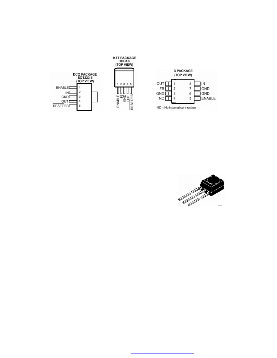
33
Plasma TV Service Manual
24/10/2003
• ±2% Output Voltage Tolerance Over Line, Load, and Temperature (–40C to 125C)
• Integrated UVLO
• Thermal and Overcurrent Protection
• 5-Lead SOT223–5 or DDPAK and 8–Pin SOP (TPS72501 only) Surface Mount Package
12.25. TSOP1836
12.25.1. Description
The TSOP18.. – series are miniaturized receivers for infrared remote control systems. PIN diode and
preamplifier are assembled on lead frame, the epoxy package is designed as IR filter. Carrier frequency
for TSOP1836 is 36kHz.
The demodulated output signal can directly be decoded by a microprocessor. The main benefit is the
reliable function even in disturbed ambient and the protection against uncontrolled output pulses.
12.25.2. Features
• Photo detector and preamplifier in one package
• Internal filter for PCM frequency
• TTL and CMOS compatibility
• Output active low
• Improved shielding against electrical field disturbance
• Suitable burst length .6 cycles/burst
Special Features
• Small size package
• Enhanced immunity against all kinds of disturbance light
• No occurrence of disturbance pulses at the output
• Short settling time after power on (<200_s)
12.26. PCF8591
12.26.1. General Description
The PCF8591 is a single-chip, single-supply low power 8-bit CMOS data acquisition device with four
analog inputs, one analog output and a serial I
2
C-bus interface.
Three address pins A0, A1 and A2 are used for programming the hardware address, allowing the use of
up to eight devices connected to the I
2
C-bus without additional hardware. Address, control and data to
and from the device are transferred serially via the two-line bidirectional I
2
C-bus.
The functions of the device include analog input multiplexing, on-chip track and hold function, 8-bit
analog-to-digital conversion and an 8-bit digital-to-analog conversion. The maximum conversion rate is
given by the maximum speed of the I
2
C-bus.
12.26.2. Features
• Single power supply
• Operating supply voltage 2.5 V to 6 V
• Low standby current
PDF created with FinePrint pdfFactory trial version
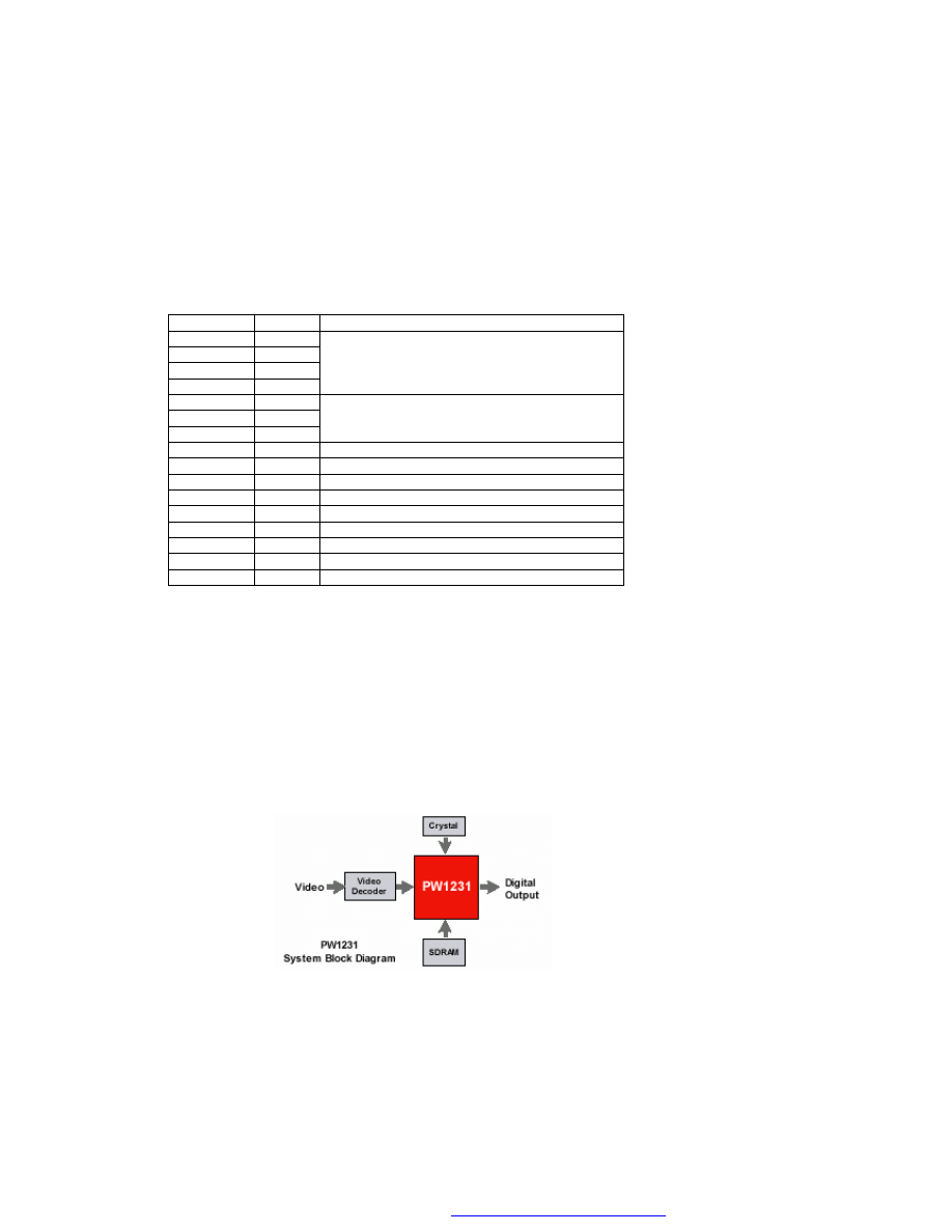
34
Plasma TV Service Manual
24/10/2003
• Serial input/output via I 2 C-bus
• Address by 3 hardware address pins
• Sampling rate given by I 2 C-bus speed
• 4 analog inputs programmable as single-ended or differential inputs
• Auto-incremented channel selection
•
Analog voltage range from
VSS
to
VDD
•
On-chip track and hold circuit
•
8-bit successive approximation A/D conversion
•
Multiplying DAC with one analog output.
12.26.3. Pinning
SYMBOL
PIN
DESCRIPTION
AINO
1
analog inputs (A/D converter)
AIN1
2
AIN2
3
AIN3
4
A0
5
hardware address
A1
6
A2
7
V
SS
8
negative supply voltage
SDA
9
I
2
C-bus data input/output
SCL
10
I
2
C-bus clock input
OSC
11
oscillator input/output
EXT
12
external/internal switch for oscillator input
AGND
13
analog ground
V
REF
14
voltage reference input
AOUT
15
analog output (D/A converter)
V
DD
16
positive supply voltage
12.27. PW1231
12.27.1. General Description
The PW1231 is a high-quality, digital video signal processor that incorporates Pixelworks’ patented
deinterlacing, scaling, and video enhancement algorithms. The PW1231 accepts industry-standard
video formats and resolutions, and converts the input into any desired output format.The video
algorithms are highly efficient, providing excellent quality video.
The PW1231 Video SignalProcessor combines many functions into a single device, including memory
controller, auto-configuration, and others. This high level of integration enables simple, flexible, cost-
effective solutions featuring fewer required components.
12.27.2. Features
• Built-In Memory Controller
• Motion-Adaptive Deinterlace Processor
• Intelligent Edge Deinterlacing
• Digital Color/Luminance Transient Improvement (DCTI/DLTI)
• Interlaced Video Input Options, including NTSC and PAL
• Independent horizontal and vertical scaling
PDF created with FinePrint pdfFactory trial version
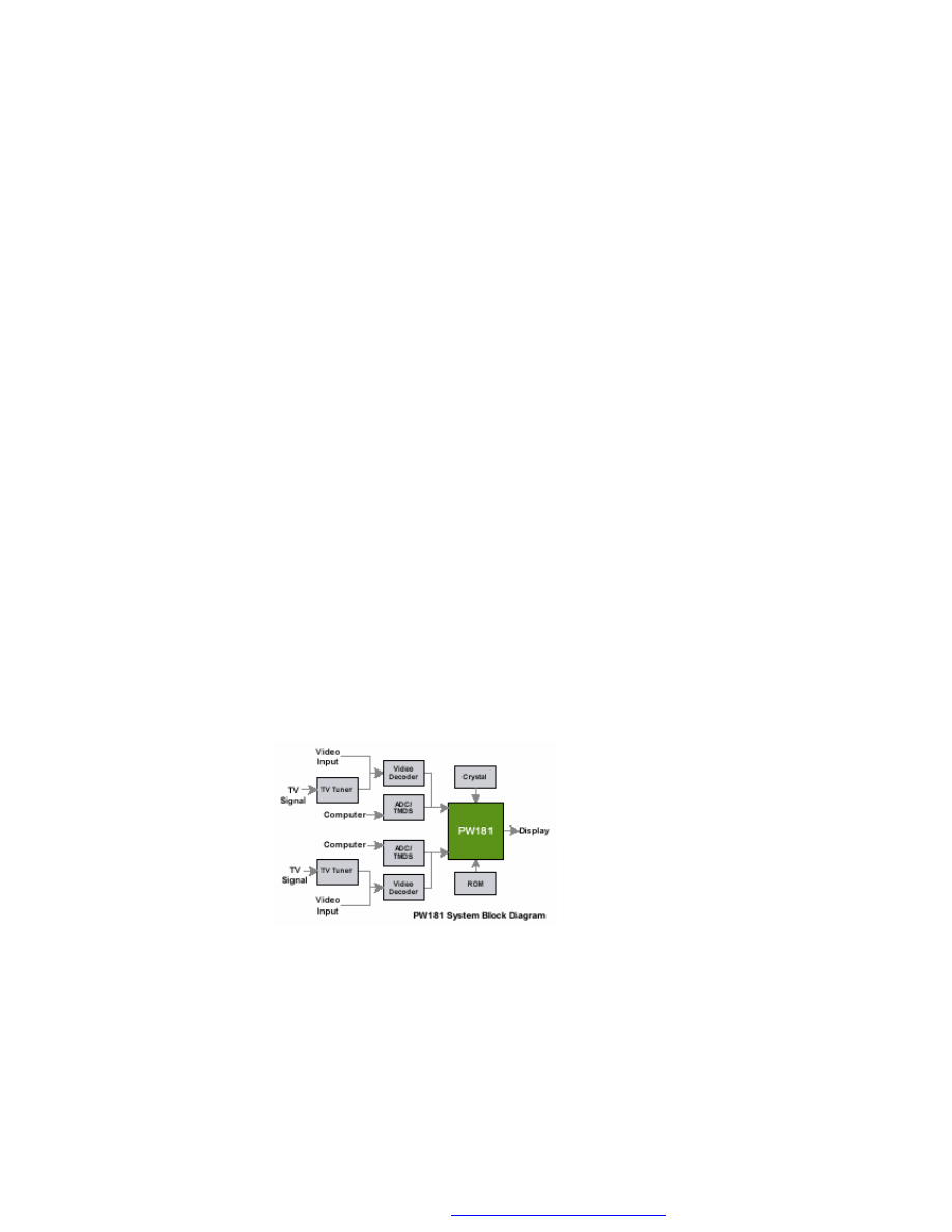
35
Plasma TV Service Manual
24/10/2003
• Copy Protection
• Two-Wire Serial Interface
12.27.3. Applications
For use with Digital Displays
• Flat-Panel (LCD, DLP) TVs
• Rear Projection TVs
• Plasma Displays
• LCD Multimedia Monitors
• Multimedia Projectors
12.28. PW181
12.28.1. General Description
The PW181 ImageProcessor is a highly integrated “system-on-a-chip” that interfaces computer
graphics and video inputs in virtually any format to a fixed-frequency flat panel display.
Computer and video images from NTSC/PAL to WUXGA at virtually any refresh rate can be resized to
fit on a fixed-frequency target display device with any resolution up to WUXGA. Video data from 4:3
aspect ratio NTSC or PAL and 16:9 aspect ratio HDTV or SDTV is supported. Multi-region, nonlinear
scaling allows these inputs to be resized optimally for the native resolution of the display.
Advanced scaling techniques are supported, such as format conversion using multiple programmable
regions. Three independent image scalers coupled with frame locking circuitry and dual programmable
color lookup tables create sharp images in multiple windows, without user intervention.
Embedded SDRAM frame buffers and memory controllers perform frame rate conversion and
enhanced video processing completely on-chip. A separate memory is dedicated to storage of on-
screen display images and CPU general purpose use.
Advanced video processing techniques are supported using the internal frame buffer, including motion
adaptive, temporal deinterlacing with film mode detection. When used in combination with the new
third-generation scaler, this advanced video processing technology delivers the highest quality video for
advanced displays.
Both input ports support integrated DVI 1.0 content protection using standard DVI receivers.
A new advanced OSD Generator with more colors and larger sizes supports more demanding OSD
applications, such as on-screen programming guides. When coupled with the new, faster, integrated
microprocessor, this OSD Generator supports advanced OSD animation techniques.
Programmable features include the user interface, custom start-up screen, all automatic imaging
features, and special screen effects.
12.28.2. Features
• Third-generation, two-dimensional filtering techniques
• Third-generation, advanced scaling techniques
• Second-generation Automatic Image Optimization
• Frame rate conversion
• Video processing
• On-Screen Display (OSD)
• On-chip microprocessor
• JTAG debugger and boundary scan
• Picture-in-picture (PIP)
PDF created with FinePrint pdfFactory trial version

36
Plasma TV Service Manual
24/10/2003
• Multi-region, non-linear scaling
• Hardware 2-wire serial bus support
12.28.3. Applications
• Multimedia Displays
• Plasma Displays
• Digital Television
12.29. SIL151B
12.29.1. General Description
The SiI 151B receiver uses PanelLink Digital technology to support high-resolution displays up to SXGA
(25-112MHz). This receiver supports up to true color panels (24 bit/pixel, 16M colors) with both one and
two pixels per clock.
All PanelLink products are designed on a scaleable CMOS architecture, ensuring support for future
performance enhancements while maintaining the same logical interface. System designers can be
assured that the interface will be stable through a number of technology and performance generations.
PanelLink Digital technology simplifies PC and display interface design by resolving many of the system
level issues associated with high-speed mixed signal design, providing the system designer with a
digital interface solution that is quicker to market and lower in cost.
12.29.2. Features
• Low Power Operation: 201mA max. current consumption at 3.3V core operation
• Time staggered data output for reduced ground bounce and lower EMI
• Sync Detect feature for Plug & Display iMHot Plugginglo
• Cable Distance Support: over 5m with twisted-pair, fiber-optics ready
• Compliant with DVI 1.0 (DVI is backwards compatible with VESA
®
P&D
TM
and DFP)
• HSYNC de-jitter circuitry enables stable operation even when HSYNC contains jitter
• Low power standby mode
• Automatic entry into standby mode with clock detect circuitry
• Standard and Pb-free packages
12.30. SDRAM 4M x 16 (MT48LC4M16A2TG-75)
12.30.1. General Description
The Micron ® 64Mb SDRAM is a high-speed CMOS, dynamic random-access memory containing
67,108,864 bits. It is internally configured as a quad-bank DRAM with a synchronous interface (all
signals are registered on the positive edge of the clock signal, CLK). Each of the x4’s 16,777,216-bit
banks is orga-nized as 4,096 rows by 1,024 columns by 4 bits. Each of the x8’s 16,777,216 -bit banks is
organized as 4,096 rows by 512 columns by 8 bits. Each of the x16’s 16,777,216- bit banks is
organized as 4,096 rows by 256 columns by 16 bits.
Read and write accesses to the SDRAM are burst oriented; accesses start at a selected location and
continue for a programmed number of locations in a programmed sequence. Accesses begin with the
registration of an ACTIVE command, which is then followed by a READ or WRITE command. The
address bits registered coincident with the ACTIVE command are used to select the bank and row to be
accessed (BA0, BA1 select the bank; A0-A11 select the row). The address bits registered coincident
with the READ or WRITE command are used to select the starting column location for the burst access.
The SDRAM provides for programmable READ or WRITE burst lengths of 1, 2, 4, or 8 locations, or the
full page, with a burst terminate option. An auto precharge function may be enabled to provide a self-
timed row precharge that is initiated at the end of the burst sequence.
The 64Mb SDRAM uses an internal pipelined architecture to achieve high-speed operation. This
architecture is compatible with the 2n rule of prefetch architectures, but it also allows the column
address to be changed on every clock cycle to achieve a high-speed, fully random access. Precharging
one bank while accessing one of the other three banks will hide the precharge cycles and provide
seamless, high-speed, random-access operation.
The 64Mb SDRAM is designed to operate in 3.3V memory systems. An auto refresh mode is provided,
along with a power-saving, power-down mode. All inputs and outputs are LVTTL-compatible.
PDF created with FinePrint pdfFactory trial version
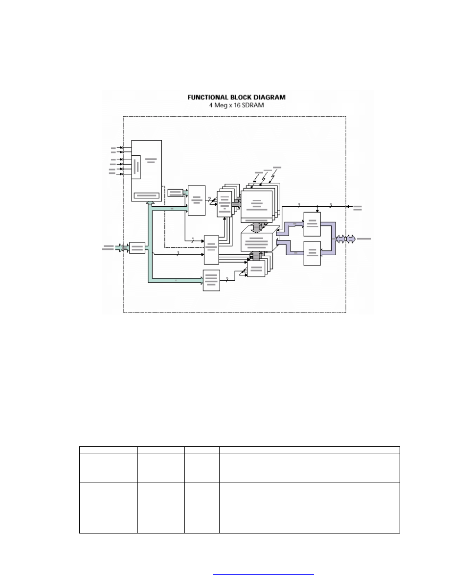
37
Plasma TV Service Manual
24/10/2003
SDRAMs offer substantial advances in DRAM operating performance, including the ability to
synchronously burst data at a high data rate with automatic column-address generation, the ability to
interleave between internal banks in order to hide precharge time and the capability to randomly
change column addresses on each clock cycle during a burst access.
12.30.2. Features
• PC66-, PC100-, and PC133-compliant
• Fully synchronous; all signals registered on positive edge of system clock
• Internal pipelined operation; column address can be changed every clock cycle
• Internal banks for hiding row access/precharge
• Programmable burst lengths: 1, 2, 4, 8, or full page
• Auto Precharge, includes CONCURRENT AUTO PRECHARGE, and Auto Refresh Modes
• Self Refresh Modes: standard and low power
• 64ms, 4,096-cycle refresh
• LVTTL-compatible inputs and outputs
• Single +3.3V ±0.3V power supply
12.30.3. Pin Descriptions
PIN NUMBERS
SYMBOL
TYPE
DESCRIPTION
38
CLK
Input
Clock: CLK is driven by the system clock. All SDRAM input
signals are sampled on the positive edge of CLK. CLK also
increments the internal burst counter and controls the output
registers.
37
CKE
Input
Clock Enable: CKE activates (HIGH) and deactivates (LOW)
the CLK signal. Deactivating the clock provides PRECHARGE
POWER-DOWN and SELF REFRESH operation (all banks
idle), ACTIVE POWER-DOWN (row active in any bank) or
CLOCK SUSPEND operation (burst/access in progress). CKE
is synchronous except after the device enters power-down and
self refresh modes, where CKE becomes asynchronous until
PDF created with FinePrint pdfFactory trial version
38
Plasma TV Service Manual
24/10/2003
after exiting the same mode. The input buffers, including CLK,
are disabled during power-down and self refresh modes,
providing low standby power. CKE may be tied HIGH.
19
CS#
Input
Chip Select: CS# enables (registered LOW) and disables
(registered HIGH) the command decoder. All commands are
masked when CS# is registered HIGH. CS# provides for
external bank selection on systems with multiple banks. CS# is
considered part of the command code.
16, 17, 18
WE#, CAS#,
RAS#
Input
Command Inputs: WE#, CAS#, and RAS# (along with CS#)
define the command being entered.
39
x4, x8: DQM
15, 39
x16:
DQML,
DQMH
Input
Input/Output Mask: DQM is an input mask signal for write
accesses and an output enable signal for read accesses. Input
data is masked when DQM is sampled HIGH during a WRITE
cycle. The output buffers are placed in a High-Z state (two-
clock latency) when DQM is sampled HIGH during a READ
cycle. On the x4 and x8, DQML (Pin 15) is a NC and DQMH is
DQM. On the x16, DQML corresponds to DQ0-DQ7 and
DQMH corresponds to DQ8-DQ15. DQML and DQMH are
considered same state when referenced as DQM.
20, 21
BA0, BA1
Input
Bank Address Inputs: BA0 and BA1 define to which bank the
ACTIVE, READ, WRITE or PRECHARGE command is being
applied.
23-26, 29-34, 22,
35
A0-A11
Input
Address Inputs: A0-A11 are sampled during the ACTIVE
command (row-address A0-A11) and READ/WRITE command
(column-address A0-A9 [x4]; A0-A8 [x8]; A0-A7 [x16]; with A10
defining auto precharge) to select one location out of the
memory array in the respective bank. A10 is sampled during a
PRECHARGE command to determine if all banks are to be
precharged (A10[HIGH]) or bank selected by BA0, BA1
(A1[LOW]). The address inputs also provide the op-code
during a LOAD MODE REGISTER command.
2, 4, 5, 7, 8, 10,
11, 13, 42, 44, 45,
47, 48, 50, 51, 53
DQ0-DQ15
x16: I/O
Data Input/Output: Data bus for x16 (4, 7, 10, 13, 42, 45, 48,
and 51 are NCs for x8; and 2, 4, 7, 8, 10, 13, 42, 45, 47, 48,
51, and 53 are NCs for x4).
2, 5, 8, 11, 44, 47,
50, 53
DQ0-DQ7
x8: I/O
Data Input/Output: Data bus for x8 (2, 8, 47, 53 are NCs for
x4).
5, 11, 44, 50
DQ0-DQ3
x4: I/O
Data Input/Output: Data bus for x4.
40
NC
–
No Connect: These pins should be left unconnected.
36
NC
–
Address input (A12) for the 256Mb and 512Mb devices
3, 9, 43, 49
V
DD
Q
Supply
DQ Power: Isolated DQ power on the die for improved noise
immunity.
6, 12, 46, 52
V
SS
Q
Supply
DQ Ground: Isolated DQ ground on the die for improved noise
immunity.
1, 14, 27
V
DD
Supply
Power Supply: +3.3V ±0.3V.
28, 41, 54
V
SS
Supply
Ground.
PDF created with FinePrint pdfFactory trial version

39
Plasma TV Service Manual
24/10/2003
12.31. FLASH 8MBit
12.31.1. Description
The M29W800A is a non-volatile memory that may be erased electrically at the block or chip level and
programmed in-system on a Byte-by-Byte or Word-by-Word basis using only a single 2.7V to 3.6V V
CC
supply. For Program and Erase operations the necessary high voltages are generated internally. The
device can also be programmed in standard programmers.
The array matrix organisation allows each block to be erased and reprogrammed without affecting o ther
blocks. Blocks can be protected against programing and erase on programming equipment, and
temporarily unprotected to make changes in the application. Each block can be programmed and
erased over 100,000 cycles.
Instructions for Read/Reset, Auto Select for reading the Electronic Signature or Block Protection status,
Programming, Block and Chip Erase, Erase Suspend and Resume are written to the device in cycles of
commands to a Command Interface using standard microprocessor write timings.
12.31.2. Features
• 2.7V to 3.6V Supply Voltage for Program, Erase and Read Operations
• Access Time: 80ns
• Programming Time: 10µs typical
• Program/Erase Controller (P/E.C.)
– Program Byte-by-Byte or Word-by-Word
– Status Register bits and Ready/Busy Output
• Security Protection Memory Area
• Instruction Address Coding: 3 Digits
• Memory Blocks
– Boot Block (Top or Bottom location)
– Parameter and Main blocks
• Block, Multi-Block and Chip Erase
• Multi Block Protection/Temporary Unprotection Modes
• Erase Suspend and Resume Modes
– Read and Program another Block during Erase Suspend
• Low Power Consumption
– Stand-by and Automatic Stand-by
• 100,000 Program/Erase Cycles per Block
• 20 Years Data Retention
– Defectivity below 1ppm/year
• Electronic Signature
– Manufacturer Code: 20h
– Top Device Code, M29W800AT: D7h
– Bottom Device Code, M29W800AB: 5Bh
PDF created with FinePrint pdfFactory trial version
40
Plasma TV Service Manual
24/10/2003
13. SERVICE MENU SETTINGS
All system, geometry and white balance alignments are performed in production service mode. Before
starting the production mode alignments, make sure that all manual adjustments are done correctly. To
start production mode alignments enter the MENU by pressing “M” button and then press the digits 4, 7,
2 and 5 respectively. The following menu appears on the screen.
There are 3 submenu in service menu. These are display, calibration and deinterlacer menus. Press
“
◄/►” buttons to select a menu title and then “▲/▼” buttons to select a menu item and “◄/►” or “OK”
buttons to set the menu item to the desired option. To exit the service menu press “M” button.
Entire service menu parameters of Plasma TV are listed below.
13.1. display menu
By pressing “
◄/►” buttons select the first icon. display menu appears on the screen.
blank color
By pressing
•/‚ button, select blank color. Press ƒ/„ button to set the blank color. The options are:
black, red, green and blue.
panel
Displays panel resolution
power on time
Displays total working time of the set
backlight on time
Displays total backlight on time of the set. (Not used for plasma displays)
blank color
panel
power on time
backlight on time
scart prescale
nicam prescale
33:5
display
black
red
green blue
33:0
Vestel V1.0.10 Release Build
32
down to change display settings
0 852x480
25
blank color
panel
power on time
backlight on time
scart prescale
nicam prescale
33:5
display
black
red
green blue
33:0
Vestel V1.0.10 Release Build
32
down to change display settings
0 852x480
25
PDF created with FinePrint pdfFactory trial version
41
Plasma TV Service Manual
24/10/2003
scart prescale
By pressing
•/‚ button, select scart prescaler. Press ƒ/„ button to set the scart prescaler. Scart
prescale can be adjusted between 0 and 127.
nicam prescale
By pressing
•/‚ button, select nicam prescaler. Press ƒ/„ button to set the nicam prescaler. Nicam
prescale can be adjusted between 0 and 127.
fm/am prescale
By pressing
•/‚ button, select fm/am prescaler. Press ƒ/„ button to set the fm/am prescaler. Fm/am
prescale can be adjusted between 0 and 127.
subwoofer corner
By pressing
•/‚ button, select subwoofer corner. Press ƒ/„ button to set the subwoofer corner.
Subwoofer corner can be adjusted between 0 and 7.
subwoofer level
By pressing
•/‚ button, select subwoofer level. Press ƒ/„ button to set the subwoofer level.
Subwoofer level can be adjusted between 0 and 32.
agc adjustment
Adjustment for automatic gain control of tuner. By pressing
•/‚ button, select agc adjustment. Press
ƒ/„ button to set the agc adjustment. Agc adjustment can be adjusted between 0 and 31.
scart prescale
nicam prescale
fm/am prescale
subwoofer corner
subwoofer layer
agc adjustment
display
right/left to adjust scart prescale
25
32
25
17
9
3
PDF created with FinePrint pdfFactory trial version
42
Plasma TV Service Manual
24/10/2003
13.2. calibration menu
By pressing “
◄/►” buttons select the second icon. calibration menu appears on the screen.
color temp
By pressing
•/‚ button, select color temp. Press ƒ/„ button to set the color temperature. The
options are: 5500K, 6500K, 7500K, 9300K and user.
user color temp
By pressing
•/‚ button, select user color temp. Press „ button to increase the user color
temperature. Press
ƒ button to decrease the user color temperature. User color temperature can be
adjusted between 5000K and 9300K.
video format
By pressing
•/‚ button, select video format. Press ƒ/„ button to set the video format. The options
are: auto, ntsc, pal, secam and ntsc japan.
color space
Displays the current color space used. RGB, YPbPr SMPTE240, YPbPr REC709 and YCbCr REC601.
test pattern
By pressing
•/‚ button, select test pattern. Press ƒ/„ button to set the test pattern. The options are:
none, solid color and vert bars.
right/left to adjust item
colorspace
test pattern
color components
solid field level
adc calibration
initial APS
factory reset
calibration
RGB
none
solid color vert bars
all
red green blue
33
on
off
<ok> to activate
color temp
user color temp
video format
colorspace
test pattern
color components
solid field level
auto
calibration
5500K
6500K
7500K 9300K user
6500K
RGB
none
solid color vert bars
all
red green blue
33
down to change cal. settings, scrolling menu
PDF created with FinePrint pdfFactory trial version

43
Plasma TV Service Manual
24/10/2003
color components
By pressing
•/‚ button, select color components. Press ƒ/„ button to set the color components.
The options are: all, red, green and blue.
solid field level
By pressing
•/‚ button, select solid field level. Press „ button to increase or ƒ button to decrease
the solid field level. Solid field level can be adjusted between 0 and 64.
adc calibration
Not used for this model.
initial APS
By pressing
•/‚ button, select initial APS. Initial aps is selected on or off. If initial aps is wanted on
startup, this item should be made on.
factory reset
By pressing
•/‚ button, select factory reset. Press “OK” button to return to the factory setting values.
PDF created with FinePrint pdfFactory trial version
44
Plasma TV Service Manual
24/10/2003
13.3. deinterlacer menu
By pressing “
◄/►” buttons select the third icon. deinterlacer menu appears on the screen.
blank expansion
By pressing
•/‚ button, select blank expansion. Blank expantion can be set to on or off by pressing
ƒ/„ button.
dcti
Digital colour transition improvement: By pressing
•/‚ button, select dcti. DCTI can be adjusted
between 0 and 255 by pressing
ƒ/„ button.
dlti
Digitial luma transition improvement: By pressing
•/‚ button, select dlti. DLTI can be adjusted
between 0 and 255 by pressing
ƒ/„ button.
luminance peaking
By pressing
•/‚ button, select luminance peaking. Luminance peaking can be set to on or off by
pressing
ƒ/„ button.
film mode
By pressing
•/‚ button, select film mode. Film mode speed can be set to on or off by pressing ƒ/„
button.
blank expansion
dcti
dlti
luminance peaking
film mode
film mode speed
vof
deinterlacer
131
down for deinterlacer settings, scrolling menu
off
on
64
off
on
off
on
3
off
on
vof
bad cut
nr threshold
noise reduction
lai level
sharpness
sparkle
deinterlacer
40
right/left to adjust item
off
on
2
off
on
low
high
10
255
PDF created with FinePrint pdfFactory trial version

45
Plasma TV Service Manual
24/10/2003
film mode speed
By pressing
•/‚ button, select film mode speed. Film mode speed can be set to 0, 1, 2 or 3 by
pressing
ƒ/„ button.
vof
video on film. By pressing
•/‚ button, select vof. VOF can be set to on or off by pressing ƒ/„ button.
bad cut
By pressing
•/‚ button, select vof. Bad cut can be set to on or off by pressing ƒ/„ button.
nr threshold
By pressing
•/‚ button, select nr threshold. Nr threshold can be set to low or high by pressing ƒ/„
button.
noise reduction
By pressing
•/‚ button, select noise reduction. Noise reduction can be adjusted between 0 and 255
by pressing
ƒ/„ button.
lai level
By pressing
•/‚ button, select lai level. Lai level can be set to 0, 1 or 2 by pressing ƒ/„ button.
sharpness
By pressing
•/‚ button, select sharpness. Sharpness can be adjusted between 0 and 255 by
pressing
ƒ/„ button.
sparkle
By pressing
•/‚ button, select sparkle. Sparkle can be adjusted between 0 and 255 by pressing ƒ/„
button.
PDF created with FinePrint pdfFactory trial version
46
Plasma TV Service Manual
24/10/2003
13.4. Service menu factory reset values
SERVICE MENU
BLANK COLOR
black
SCART PRESCALE
15
NICAM PRESCALE
32
FM/AM PRESCALE
14
SUBWOOFER CORNER
5
SUBWOOFER LEVEL
32
DISPLAY
AGC
16
COLOR TEMPERATURE
6500
COLOR TEMPERATURE-USER
6500
VIDEO FORMAT
AUTO
COLOR SPACE
autodetected
TEST PATTERN
none
COLOR COMPONENTS
all
SOLID FIELD LEVEL
33
CALIBRATION
INITIAL APS
on
BLACK EXPANSION
DCTI
DLTI
LUMINANCE PEAKING
FILM MODE
FILM MODE SPEED
VOF
BAD CUT
NR THRESHOLD
NOISE REDUCTION
LAI LEVEL
SHARPNESS
DEINTERLACER
SPARKLE
These values are not
recorded, for this reason
they are adjusted to a
specified value.
PDF created with FinePrint pdfFactory trial version
47
Plasma TV Service Manual
24/10/2003
14. BLOCK DIAGRAM
AUDIO
DECODING
MSP34XX
MICRONAS
AUDIO
AMPLIFIER
TDA7265L
ST
MAIN_L,
MAIN_R,
SAA7118E
VIDEO PROCESSOR
MAIN PICTURE
PHILIPS
SAA7118E
VIDEO PROCESSOR
PIP PICTURE
PHILIPS
PW181
A
U
D
IO
/V
ID
E
O
/G
R
A
P
H
IC
S
I
N
/O
U
T
AUDIO AMPL. BOARD
1-LAYER
A/V BOARD
6-LAYER
DS090C385 LVDS
Tx NATIONAL
24-bit RGB
I2C
HS, VS,
DE, CLK
AD9883 ANALOG DEVICE
ADC
SIL151 SILICON
IMAGE
DVI Rx
YUV
16-bit
YUV
16-bit
24-bit RGB
48-bit
dual
RGB
SIL164
DVI OUTPUT
PW1231
RGB
24-bit
OPTIONAL
V
M
B
w
ith
P
ix
e
lw
o
rk
s
4
S
c
a
rt
GENERAL BLOCK DIAGRAM
PDF created with FinePrint pdfFactory trial version
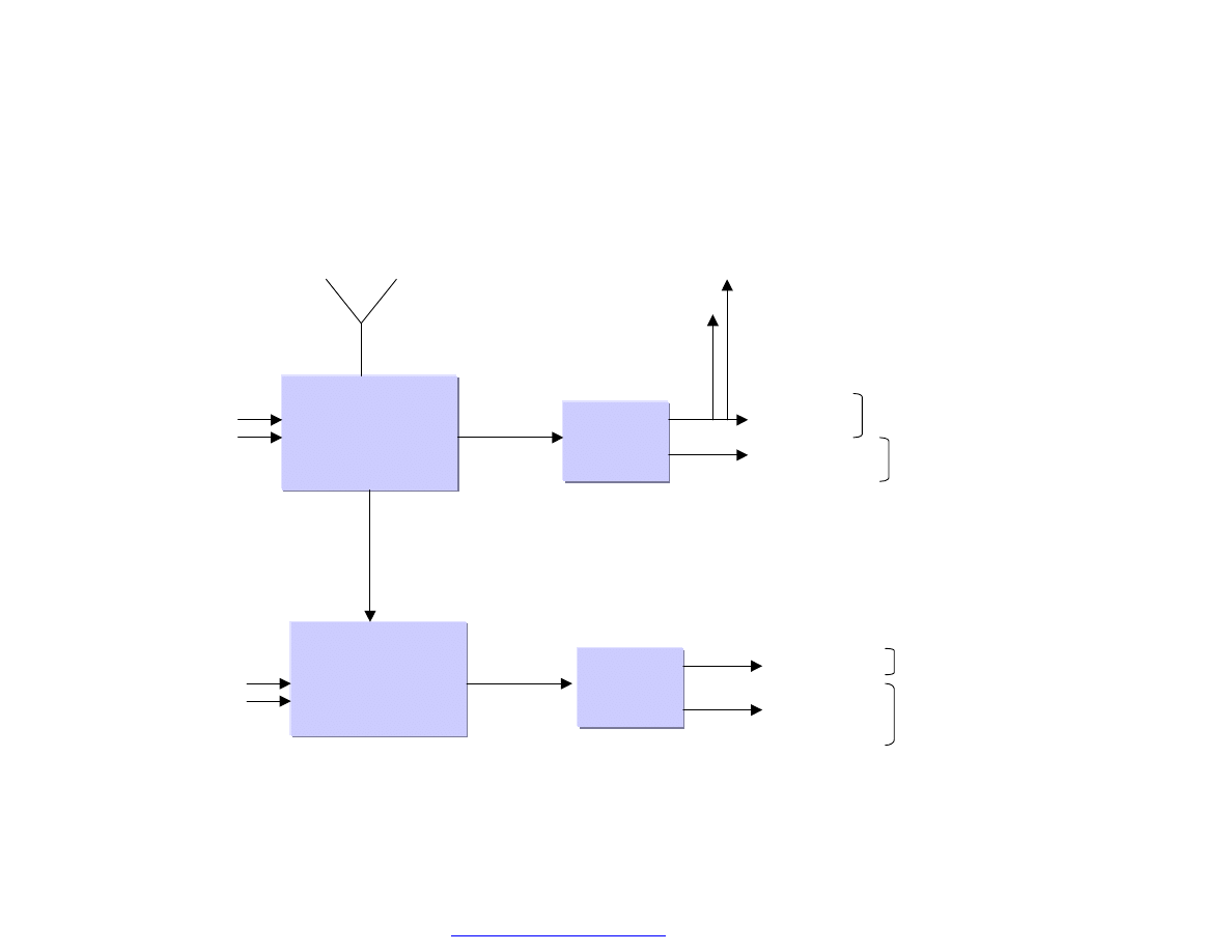
48
Plasma TV Service Manual
24/10/2003
UV1316
Tuner 1
Philips
UV1316
Tuner 2
Philips
PHILIPS
IF IC 1
TDA9886
I2C
I2C
IF 1
TUN1_CVBS
TUN1_QSS1
SC1_V_OUT
PHILIPS
IF IC 2
TDA9886
IF 2
TUN2_CVBS
TO TEA6415
VIDEO SWITCH
TO MSP3411G
AUDIO PROCESSOR
FOR MAIN SOUND
TO TEA6415 PIP
VIDEO SWITCH
A/V BOARD
6-layer
SC3_V_OUT
TUN2_QSS2
TO MSP3411G
AUDIO PROCESSOR
FOR MAIN SOUND
TUNER&IF BLOCK
PDF created with FinePrint pdfFactory trial version
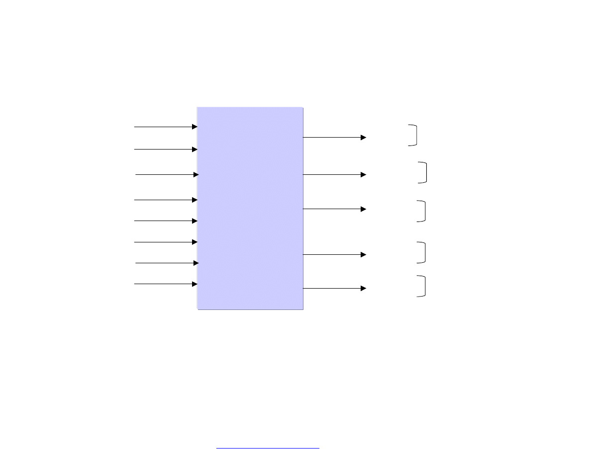
49
Plasma TV Service Manual
24/10/2003
TEA6415C
VIDEO SWITCH
ST
SC1_V_IN
SC2_V_IN
PIP_CVBS
AV1_V_IN
SC3_V_IN
FAV_CVBS
VxtoSAA7118
MP
SELECTED VIDEO
TO SAA7118 MP
FOR
MAIN PICTURE
VxtoSAA7118
PIP
SELECTED VIDEO
TO SAA7118 PIP FOR
PIP PICTURE
SC4_V_OUT
SC2_V_OUT
AV1_V_OUT
SELECTABLE
VIDEO OUT
FOR AV1
A/V BOARD
6-layer
TUN1_CVBS
SC4_V_IN
SELECTABLE
VIDEO OUT
FOR SCART 4
SELECTABLE
VIDEO OUT
FOR SCART 2
VIDEO MATRIXING
PDF created with FinePrint pdfFactory trial version

50
Plasma TV Service Manual
24/10/2003
TEA6420
AUDIO SWITCH
ST
SC4_AUDIO_L/R_IN
A/V BOARD
6-layer
SC2_AUDIO_L/R_IN
FAV_AUDIO_L/R_IN
SC3_AUDIO_L/R_IN
ASW_AUDIO_L/R_IN
BAV_AUDIO_L/R_OUT
SC4_AUDIO_L/R_OUT
ASW_AUDIO_L/R_OUT
SC2_AUDIO_L/R_OUT
MSP
SC4_AUDIO_L/R_IN
SC2_AUDIO_L/R_IN
FAV_AUDIO_L/R_IN
SC3_AUDIO_L/R_IN
ASW_AUDIO_L/R_IN
BAV_AUDIO_L/R_OUT
SC4_AUDIO_L/R_OUT
ASW_AUDIO_L/R_OUT
SC2_AUDIO_L/R_OUT
HEADPHONE
AUDIO MATRIXING
PDF created with FinePrint pdfFactory trial version
51
Plasma TV Service Manual
24/10/2003
SCART
3
SC1_AUDIO_R_OUT
SC1_AUDIO_L_OUT
SC1_AUDIO_R_IN
SC1_AUDIO_L_IN
SC3_V_OUT
SC3_V_IN
SC3_PIN8
INTO/FROM
AUDIO MATRIX
FROM TEA6415 VIDEO SWITCH
INTO TEA6415 VIDEO SWITCH
INTO PCF8591
A/V BOARD
6-layer
SCART
2
SC2_AUDIO_R_OUT
SC2_AUDIO_L_OUT
SC2_AUDIO_R_IN
SC2_AUDIO_L_IN
SC2_V_OUT
SC2_V_IN
SC2_PIN8
INTO/FROM
AUDIO MATRIX
FROM TEA6415 VIDEO SWITCH
INTO TEA6415 VIDEO SWITCH
SVHSfromSC2_C
SC2_FB
INTO VPC3230D
SCART
1
SC1_AUDIO_R_OUT
SC1_AUDIO_L_OUT
SC1_AUDIO_R_IN
SC1_AUDIO_L_IN
SC2_B
SC2_G
SC2_R
SC1_FB
SC1_V_OUT
SC1_V_IN
SC1_PIN8
INTO/FROM
AUDIO MATRIX
INTO RGB
SWITCH
FROM TUN1_CVBS
SC1_B
SC1_G
INTO RGB
SWITCH
SC1_R
SCART
4
SC4_AUDIO_R_OUT
SC4_AUDIO_L_OUT
SC4_AUDIO_R_IN
SC4_AUDIO_L_IN
SC4_V_OUT
SC4_V_IN
SC4_PIN8
INTO/FROM
AUDIO MATRIX
FROM TEA6415 VIDEO SWITCH
INTO TEA6415 VIDEO SWITCH
INTO PCF8591
INTO PCF8591
INTO PCF8591
A/V IN/OUT
PDF created with FinePrint pdfFactory trial version
52
Plasma TV Service Manual
24/10/2003
D-SUB
15
PC_R_IN
PC_G_IN
PC_B_IN
PC_HS
PC_VS
DDC_CLK_PC
DDC_DATA_PC
INTO ADC 9883
INTO ADC9883
INTO PW181
DVI
SOCKET
DVI_RX0+
DVI_RX0-
DVI_RX1+
DVI_RX1-
DVI_RX2+
DVI_RX2-
DVI_RXC+
DVI_RXC-
ANA_VS_DVI
DDC_DATA_DVI
DDC_CLK_DVI
TMDS SIGNAL INTO SIL151B
FOR DECODING INTO
2 PIXEL/CLK 48 BIT RGB
INTO PW181
PC_AUDIO_R_IN
PC_AUDIO_L_IN
A/V BOARD
6-layer
AV1_V_OUT
AV1_AUDIO_L_OUT
AV1_AUDIO_R_OUT
AV1_V_IN
AV1_AUDIO_L_IN
AV1_AUDIO_R_IN
AV1 IN/OUT
FROM MSP3411G
INTO MSP3411G
FROM TEA6415
INTO TEA6415
CIN
SVHS_Y_IN
S-VIDEO
INTO SAA7118
INTO SAA7118
GRAPHICS & VIDEO IN/OUT
PDF created with FinePrint pdfFactory trial version
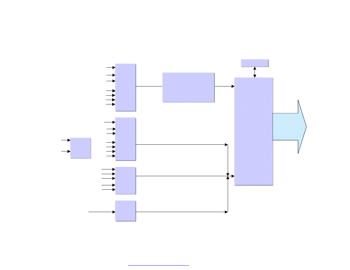
53
Plasma TV Service Manual
24/10/2003
PW181
De-interlacer
FRC
Scaler
OSD
Gamma
Correction
ROM
VRGB
GRGB
SAA
7118
MP
SAA
7118
PIP
VxtoSAA7118_MP
VxtoSAA7118_PIP
AD9883
SIL151
DVI Input
24-bit RGB
48-bit RGB
16-bit YUV
PW1231
DE-INTERLACER
24-bit
RGB
SVIDEO1_C
SVIDEO1_Y
SVIDEO1_C
SVIDEO1_Y
TXT/CC_FB
TXT/CC_R
TXT/CC_G
TXT/CC_B
TXT/CC_FB
TXT/CC_R
TXT/CC_G
TXT/CC_B
TXT/CC_R
TXT/CC_G
TXT/CC_B
16-bit YUV
Progressive or
Interlaced
24-bit dual RGB,
HS, VS, DE,
PCLK, Parity
PC_R_IN
PC_G_IN
PC_B_IN
PC_HS
PC_VS
SC_B
SC_G
SC_R
SC_FB
PI5
V330
SCART1
RGB,FB
SCART2
RGB,FB
SC_B
SC_G
SC_R
SC_FB
PI5
V330
SCART1
RGB,FB
SCART2
RGB,FB
VIDEO & IMAGE PROCESSING
PDF created with FinePrint pdfFactory trial version
54
Plasma TV Service Manual
24/10/2003
TELETEXT
SAA5264
PHILIPS
CVBS_
for TELETEXT
TXT/CC_R
TXT/CC_FB
TXT/CC_G
TXT/CC_B
FROM VIDEO
SWITCH
INTO SAA7118
RGB/FB PORTS
PIN 8
SWITCHING
PCF8591
SC2 PIN8
SC2 PIN8
SC3 PIN8
SC3 PIN8
SC1 PIN8
SC1 PIN8
SC4 PIN8
SC4 PIN8
I2C COMMUNICATION
TELETEXT DECODING & PIN8 SWITCHING
PDF created with FinePrint pdfFactory trial version

55
Plasma TV Service Manual
24/10/2003
1. SCART 1 CVBS INPUT
2. SCART 2 CVBS INPUT
3. SCART 3 CVBS INPUT
4. SCART 4 CVBS INPUT
5. SCART 1 RGB FB INPUT
6. SCART 2 RGB FB INPUT
7. BAV IN
8. FAV IN
9. FRONT SVHS IN
10. VGA INPUT
11. DVI INPUT
12. MAIN TUNER
13. PIP TUNER
1. SCART 1 CVBS OUT
2. SCART 2 CVBS OUT
3. SCART 3 CVBS OUT
4. SCART 4 CVBS OUT
5. BAV OUT
6. LVDS OUT
7. DVI OUT
INPUT & OUTPUTS
13 DIFFERENT INPUT & 7 OUTPUT
PDF created with FinePrint pdfFactory trial version
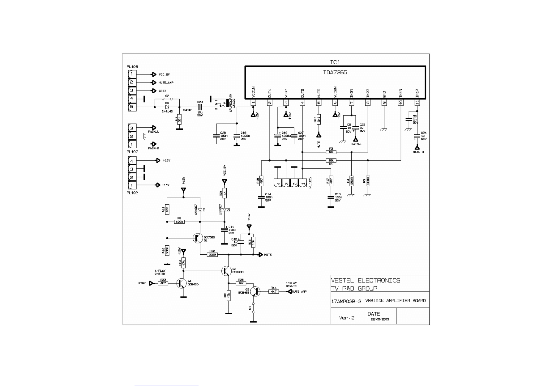
56
Plasma TV Service Manual
24/10/2003
15. CIRCUIT DIAGRAMS
17AMP02-B2
PDF created with FinePrint pdfFactory trial version
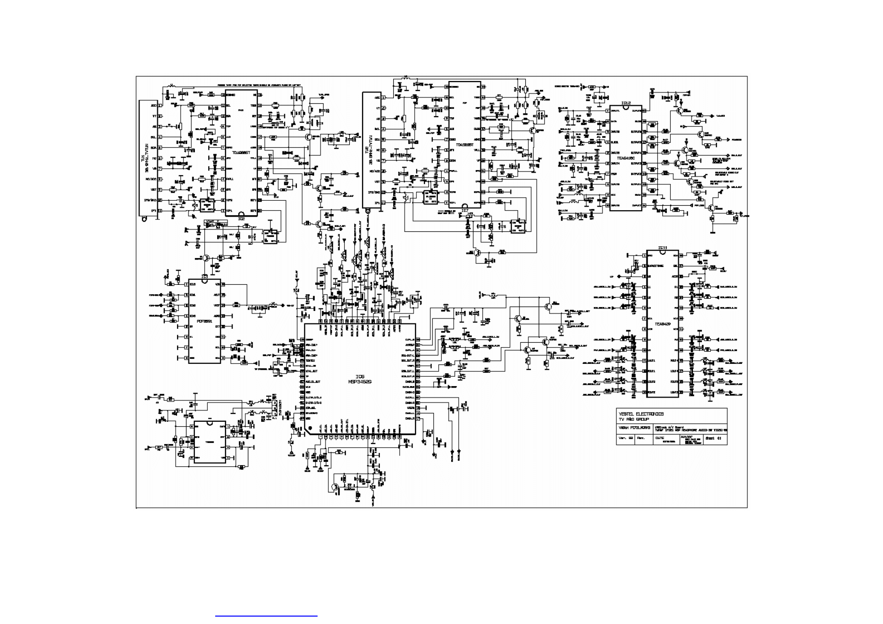
57
Plasma TV Service Manual
24/10/2003
17MB05-E2
PDF created with FinePrint pdfFactory trial version
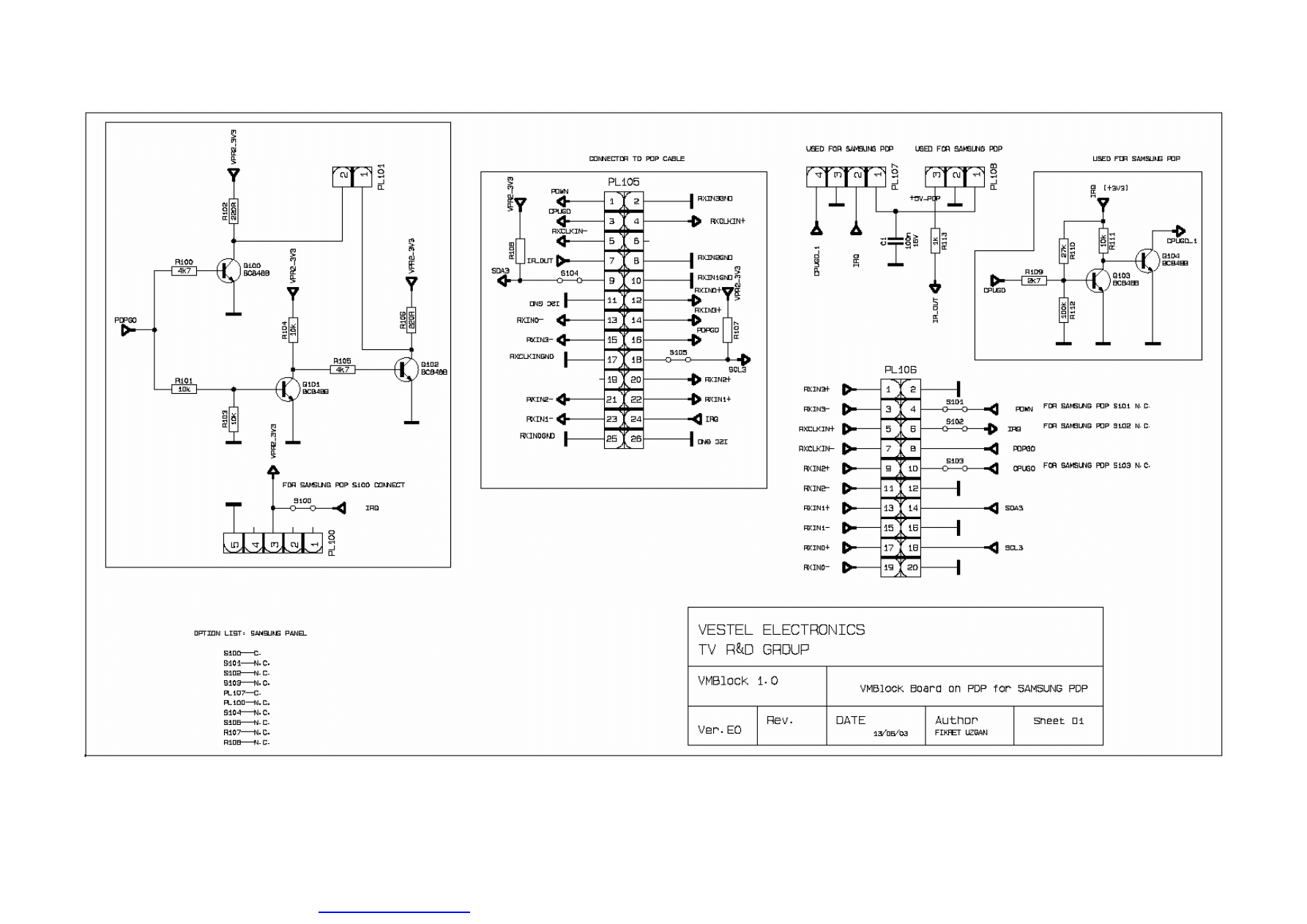
58
Plasma TV Service Manual
24/10/2003
17PDP03-1
PDF created with FinePrint pdfFactory trial version
59
Plasma TV Service Manual
24/10/2003
17LD05
PDF created with FinePrint pdfFactory trial version
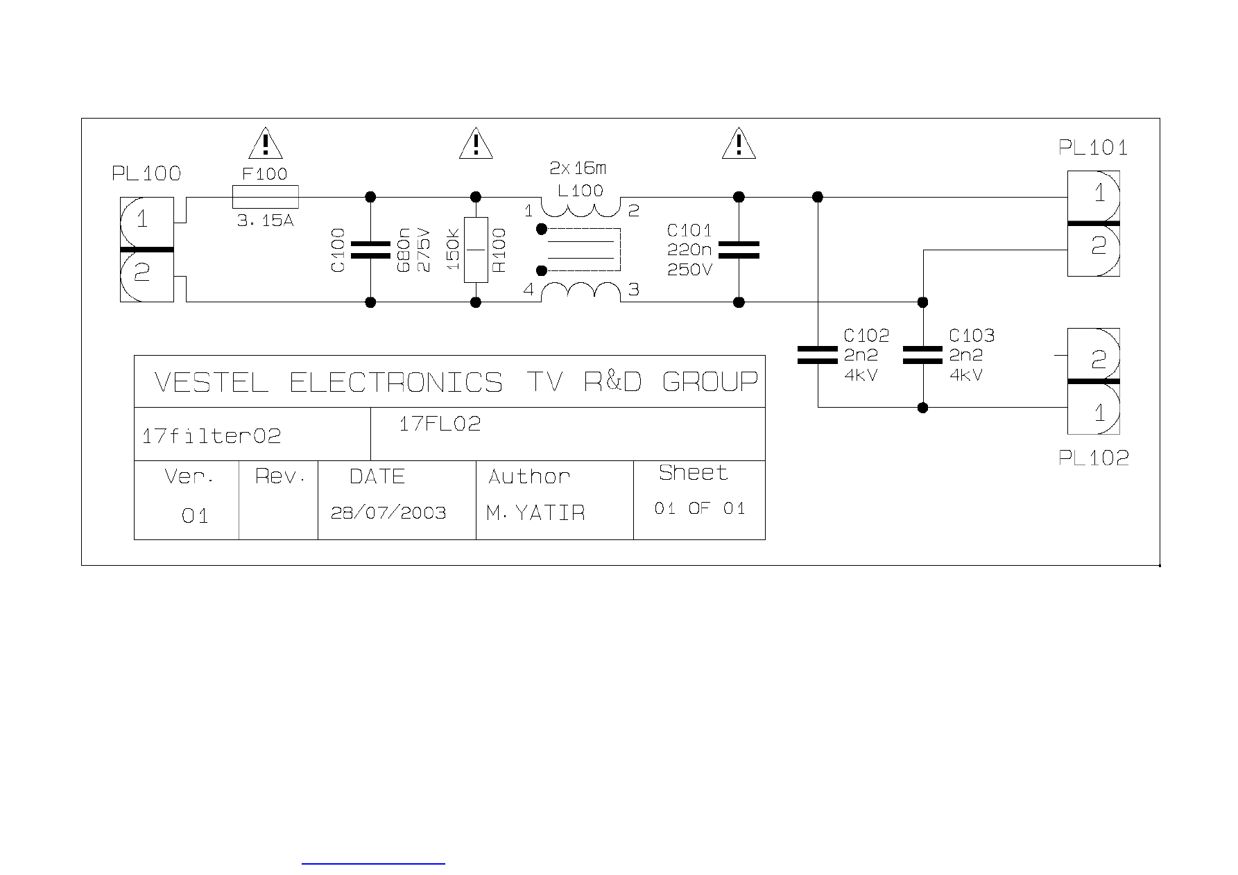
60
Plasma TV Service Manual
24/10/2003
17FL02
PDF created with FinePrint pdfFactory trial version
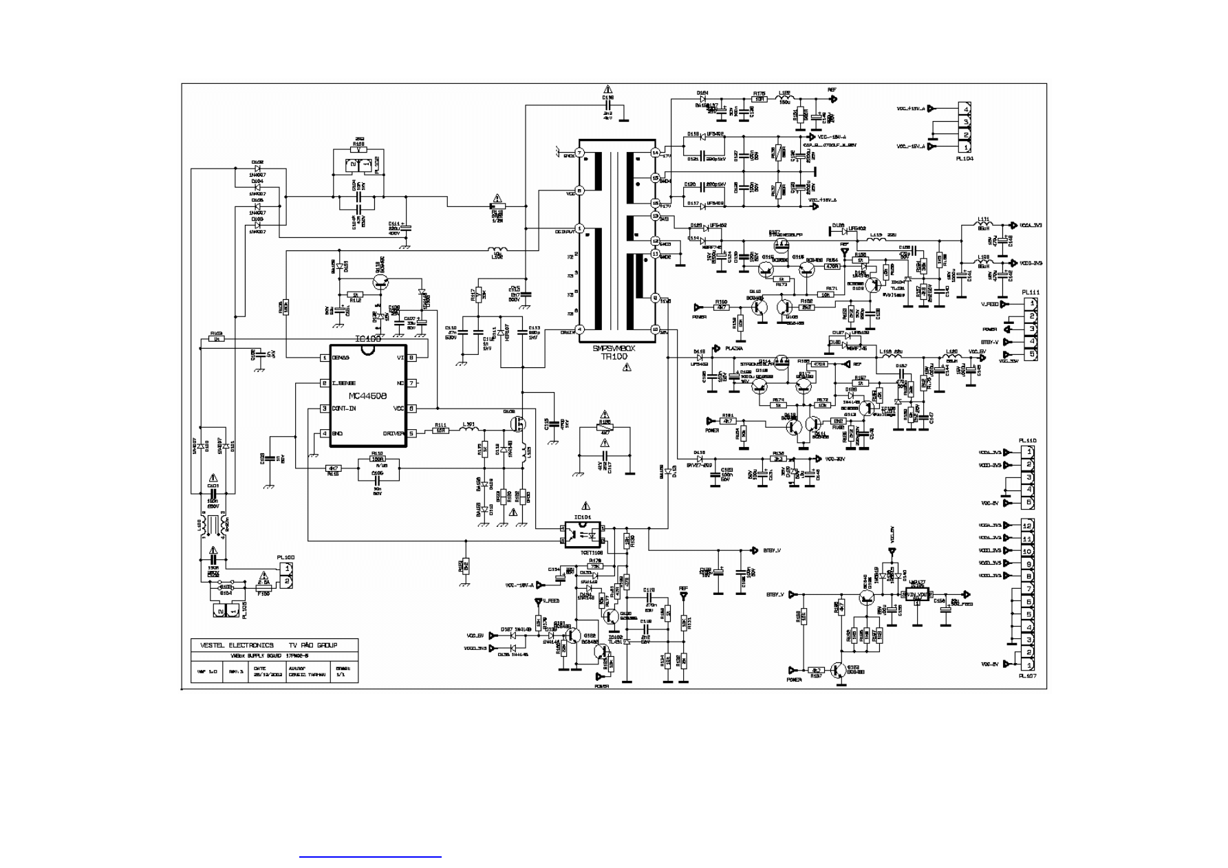
61
Plasma TV Service Manual
24/10/2003
17PW02-5
PDF created with FinePrint pdfFactory trial version
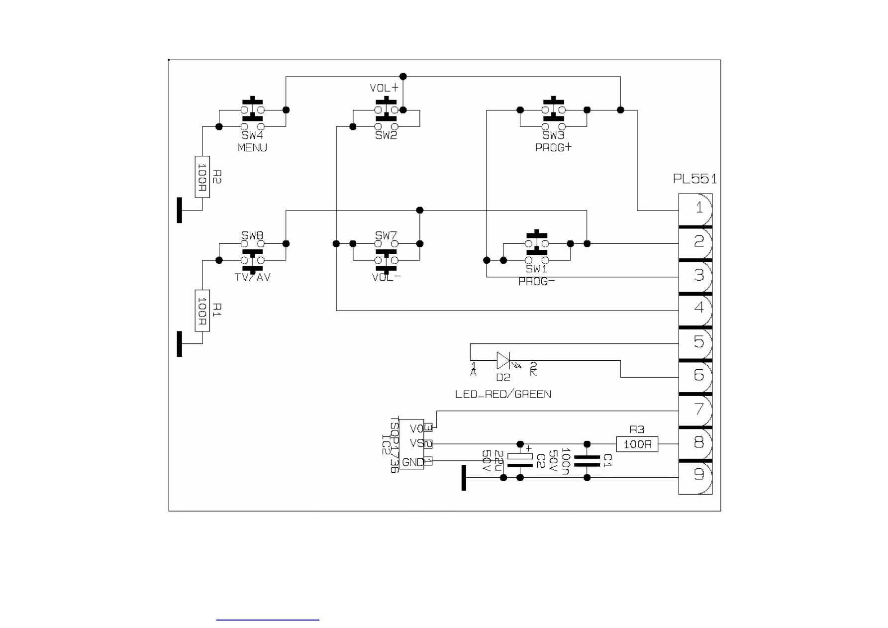
62
Plasma TV Service Manual
24/10/2003
17TK09-2
PDF created with FinePrint pdfFactory trial version
Wyszukiwarka
Podobne podstrony:
LG 42V7 Module Plasma TV Service Guide Rev2
20 TFT Service Manual TV VESTEL
31 Service Manual Installation manual for digital TV tuner
TV 486 Service Manual
hplj 5p 6p service manual vhnlwmi5rxab6ao6bivsrdhllvztpnnomgxi2ma vhnlwmi5rxab6ao6bivsrdhllvztpnnomg
Oberheim Prommer Service Manual
Korg SQ 10 Service Manual
MAC1500 service manual
Kyocera Universal Feeder UF 1 Service Manual
Proview RA783 LCD Service Manual
indesit witp82euy Service Manual
Glow Worm installation and service manual Hideaway 70CF UIS
Proview PZ456 LCD Service Manual
Glow Worm installation and service manual Ultimate 50CF UIS
ewm2000 service manual
więcej podobnych podstron