
602
IEEE TRANSACTIONS ON INDUSTRIAL ELECTRONICS, VOL. 45, NO. 4, AUGUST 1998
A Novel Switch-Mode DC-to-AC Inverter
with Nonlinear Robust Control
Zaohong Yang,
Student Member, IEEE,
and Paresh C. Sen,
Fellow, IEEE
Abstract— A switch-mode dc-to-ac inverter based on a dc-to-
dc converter topology using a novel nonlinear robust control to
generate a sinusoidal output waveform is presented. The control
scheme is based on simultaneous feedback of the output voltage
and feedforward of the input voltage and inductor voltage. As a
result, the output voltage remains dynamically unchanged when
there are large disturbances in input voltage or load current.
The nature of the control law is explained. Computer simulation
results show the robustness and fast dynamical response of
the control system. The experimental results are presented to
verify the analysis and demonstrate the feasibility of the control
strategy.
Index Terms— Control techniques, dc–ac power conversion,
dynamic response, pulsewidth modulated inverters.
I. I
NTRODUCTION
S
WITCH-MODE dc-to-ac inverters have been used in var-
ious types of applications, such as uninterruptible power
supplies, communication ring generators, aerospace power
systems, and variable-speed ac machine drives. The loads in
the aforementioned applications are either critical or sensitive.
A good steady-state and dynamic performance of the switch-
mode dc-to-ac inverter is desirable for these applications.
Traditionally, a bridge configuration is employed for the
switch-mode dc-to-ac inverters. By using a pulsewidth mod-
ulation (PWM) switching technique, the input dc voltage is
transformed into a high-frequency pulse waveform at the
output of the bridge. Through a filter, this high-frequency
pulsed voltage is smoothed into a sinusoidal waveform, as
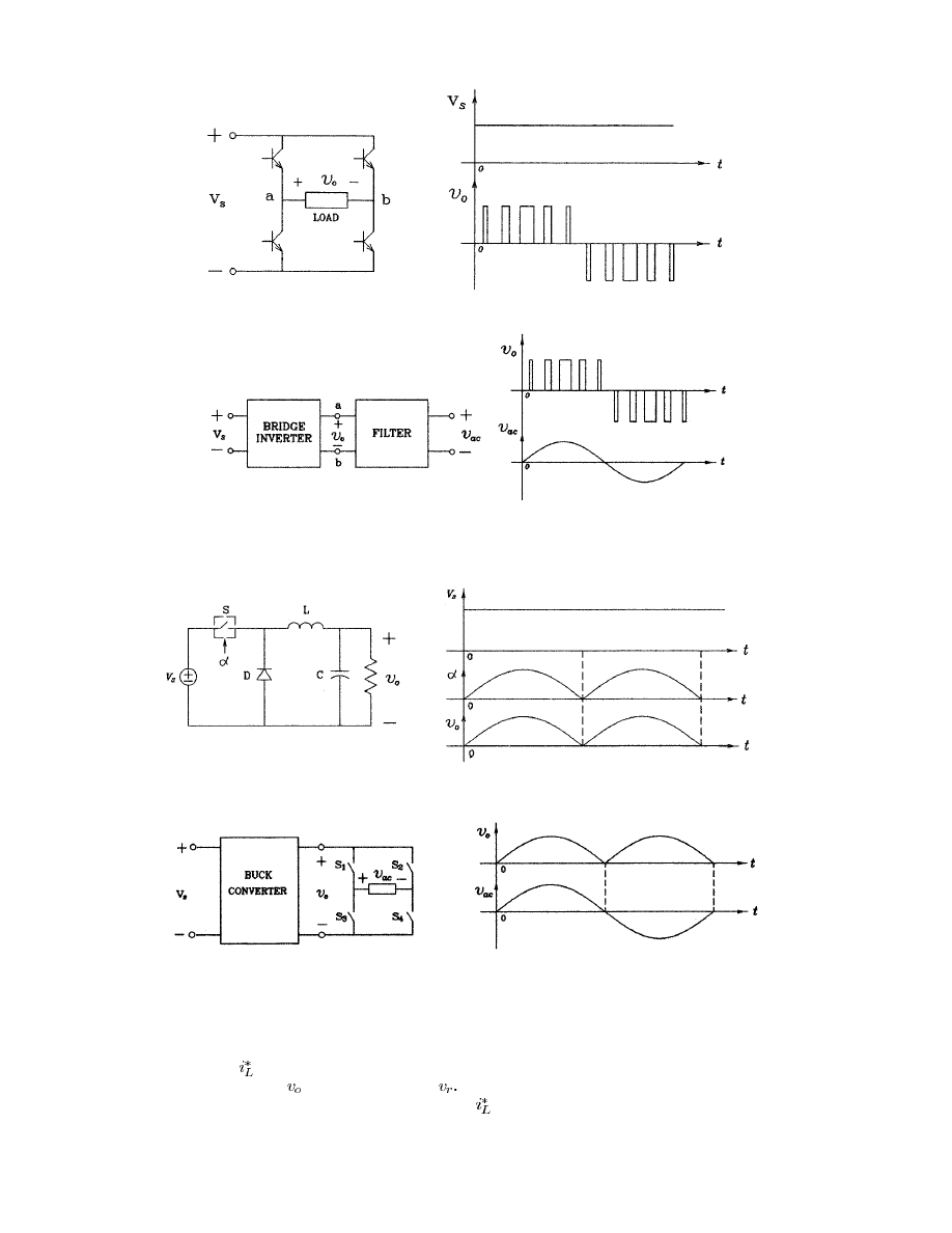
shown in Fig. 1 [1], [2].
Recently, switch-mode dc-to-ac inverters using a dc-to-dc
converter topology have been developed [3]–[7]. The principle
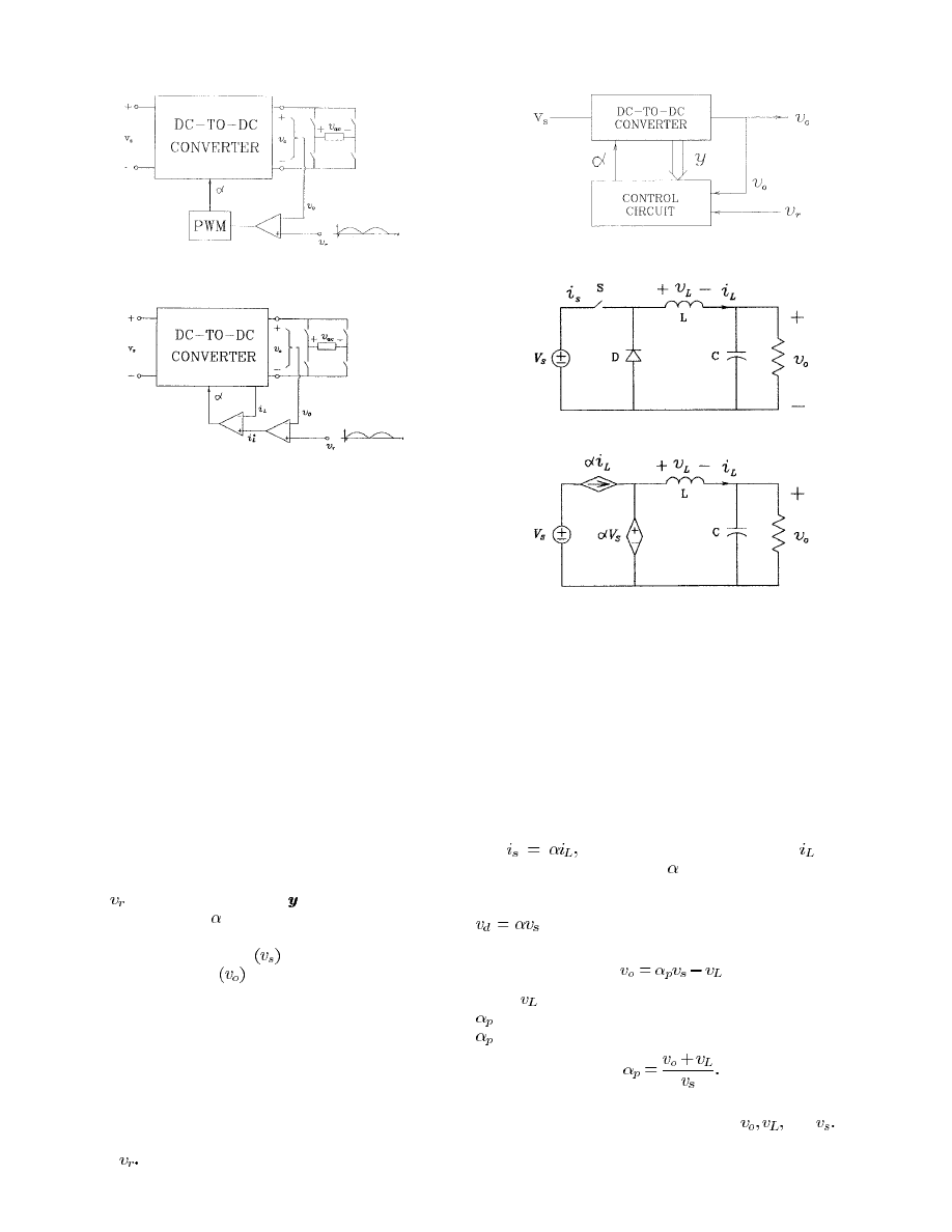
of operation of this type of inverter is illustrated in Fig. 2(a),
where the dc-to-dc converter is of buck configuration. The
average output voltage of this buck converter,
, is the
product of duty ratio
and the input voltage
i.e.,
If the input voltage
is constant and the duty ratio
is varied
slowly, relative to the switching frequency, in the form of a
fully rectified sinusoidal wave, the output
will naturally be
a fully rectified sine wave. Through a bridge circuit which is
synchronized with the fully rectified sine waveform of
the
output
is “unfolded” into a sinusoidal waveform
, as
shown in Fig. 2(b).
Manuscript received May 7, 1997; revised February 7, 1998. Abstract
published on the Internet May 1, 1998.
The authors are with the Department of Electrical and Computer Engineer-
ing, Queen’s University, Kingston, Ont., K7L 3N6, Canada.
Publisher Item Identifier S 0278-0046(98)05681-0.
Compared to the bridge-type inverter, the inverter using
a dc-to-dc converter configuration has several advantages.
Only one switch operates at high frequency and, as a result,
switching losses will be significantly less. The conduction
loss will be slightly higher because of one extra switch
compared to the bridge configuration. The overall losses will
be less, thereby increasing efficiency. In addition, the output
filtering capacitors in the dc-to-dc converters can be a dc-type
capacitor, e.g., an electrolytic capacitor which is smaller and
less expensive than the ac-type capacitor for the same capacity
required in the bridge configuration. However, the inverters
using bridge configuration must use an ac-type capacitor as
a filter. More important is that, with a dc-to-dc converter
topology, the advanced control techniques, such as current-
mode control, digital data sampling control, and sliding-mode
control, etc., developed from the investigations of dc-to-dc
converters can be directly applied to the dc-to-ac switch-
mode inverter. Therefore, a good dynamic performance can
be achieved.
The application environment of the switch-mode dc-to-ac
inverter requires that its output voltage remains dynamically
stable when the supply voltage or load current suddenly
changes.
Greater attention has been paid to the switch-mode dc-to-ac
inverter using the dc-to-dc converter topology because of the
aforementioned advantages. Several efforts have been made to
improve the dynamical performance of this type of inverter,
i.e., the output voltage remains dynamically unchanged when
subjected to large disturbances in supply voltage or load
current.
Direct duty ratio control is the most commonly used control
strategy [4]. The principle of the control strategy is illustrated
in Fig. 3. Its duty ratio is controlled by the “error” that is
the difference between the actual output voltage
and the
reference voltage
, where the reference signal consists of
a fully rectified sinusoidal waveform. The objective of the
direct duty ratio control is to stabilize the output voltage
when the system is subjected to disturbances. However, this
control method cannot achieve the dynamical stabilization of
the voltage, because the output voltage
changes before the
control action begins. A sharp overshoot will occur and a
considerable time will be taken before the voltage returns to
its steady-state value.
The application of current mode control to the switch-
mode of the dc-to-ac inverter using the dc-to-dc converter
configuration was presented in [6] and is shown in Fig. 4. In
this control strategy, the inductor current
is forced to follow
0278–0046/98$10.00
1998 IEEE
YANG AND SEN: A NOVEL SWITCH-MODE DC-TO-AC INVERTER WITH NONLINEAR ROBUST CONTROL
603
(a)
(b)
Fig. 1.
PWM bridge-type inverter. (a) Bridge-type inverter and PWM waveform at the output. (b) Bridge circuit followed by a filter to generate sine wave.
(a)
(b)
Fig. 2.
Switch-mode dc-to-ac inverter using buck converter configuration. (a) Buck converter with duty ratio varying in the form of a fully rectified
sine wave. (b) A bridge synchronizer following the buck converter.
the current control signal
, which is in proportion to the
difference between output voltage
and reference signal
This type of control strategy has many advantages over direct
duty ratio control, such as a wide bandwidth, fast response,
and automatic current protection [10], [11]. However, robust
control of the output voltage is still not achieved by this control
strategy. When the supply voltage or load current changes, the
output voltage will change at first. The current control signal
changes to accommodate the new operating condition only
after the output voltage changes.
Discrete data sampling control has also been tried with a
switch-mode dc-to-ac inverter using the dc-to-dc converter
604
IEEE TRANSACTIONS ON INDUSTRIAL ELECTRONICS, VOL. 45, NO. 4, AUGUST 1998
Fig. 3.
Block diagram of the direct duty ratio control.
Fig. 4.
Block diagram of the current-mode control.
configuration [7]. Unfortunately, the digital control is slower in
instantaneous response than the analog control. The transient
performance of the output voltage is not improved. Moreover,
this control system is very complicated and is difficult to
implement in a practical circuit.
The previously proposed control strategies for a dc-to-
ac inverter have not yet achieved the desirable dynamical
stabilization of the output voltage. In this paper, a nonlinear
control strategy which is based on the control law presented in
[8] is proposed and implemented to achieve the robust control
of the output voltage. The principle of operation of the control
technique is discussed in Section II. The simulation results
are presented in Section III. The experimental implementation
is described in Section IV. Finally, Section V gives the
conclusions.
II. P
RINCIPLE OF
O
PERATION
A switch-mode dc-to-dc converter is generally composed
of two basic parts. One is the power stage, or the switching
converter; the other is the control circuit, as shown in Fig. 5,
where
is the reference voltage,
denotes the combination
of the feedbacks, and
is the duty ratio.
The power stage controls the power absorbed from the
unregulated supply voltage
and provides a regulated
constant output voltage
at the load. The main purpose of
the control circuit is to generate a proper duty ratio according
to the conditions of the circuit so that the variation of the
output voltage is reduced as much as possible when the supply
voltage or load current changes. In order to achieve robust
control of the output voltage, i.e., to eliminate the effect of the
supply voltage or load current disturbance, the control strategy
and feedbacks should be properly selected so that the closed-
loop output voltage is independent of either the supply voltage
or the load current and is determined only by the reference
voltage
Fig. 5.
General block diagram of PWM dc-to-dc converter.
(a)
(b)
Fig. 6.
Buck converter: (a) topology and (b) its low-frequency average
model.
A nonlinear control strategy can be applied to the buck-
type dc-to-dc converter to realize the above objective. The
low-frequency averaged equivalent model of a buck converter
is shown in Fig. 6. This equivalent circuit can be derived from
the state-space average method [9]. This model is valid only
for continuous conduction mode operation.
In this averaged-circuit model, the active switch is modeled
by a controlled current source with its value equal to the
average current flowing through it over one switching cycle,
i.e.,
for the buck converter, where “
” is the
averaged inductor current and
is the duty ratio. The average
output voltage across the diode over one switching cycle is
modeled as a controlled voltage source with its value equal to
for the buck converter.
From Fig. 6(b), the output voltage can be expressed as
(1)
where
is the averaged value of the inductor voltage and
is the duty ratio required for the switching converter. This
can be expressed as
(2)
Equation (2) defines the duty ratio required by the buck
converter at a specific operating point of
and
The control circuit can now be constructed to generate the
duty ratio. Let the input and output relation of the control
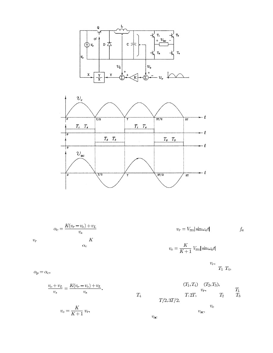
YANG AND SEN: A NOVEL SWITCH-MODE DC-TO-AC INVERTER WITH NONLINEAR ROBUST CONTROL
605
(a)
(b)
Fig. 7.
The proposed dc-to-ac inverter using nonlinear robust control system. (a) The diagram of the proposed inverter. (b) The sinusoidal output voltage
is obtained by the bridge-type synchronizer.
circuit be formulated as
(3)
where
is the reference voltage,
is the gain of the
proportional error amplifier, and
denotes the duty ratio
generated by the control circuit. The implementation is shown
in Fig. 7(a).
In the practical circuit, the output of the control circuit is
connected to the gate of the active switch in the power stage,
making
Therefore, the closed-loop characteristic can
be obtained by equating (2) and (3) as
(4)
From (4), the output voltage can be found as
(5)
Equation (5) shows that, by the control law (3), the closed-
loop averaged output voltage is forced to be proportional to
a reference voltage.
In the switch-mode dc-to-ac inverter using the buck con-
verter topology, the reference is chosen to be a fully rectified
sinusoidal wave, i.e.,
(the frequency
is
much lower than the switching frequency). The output voltage
of the buck converter can be derived as
(6)
and represents a fully rectified sinusoidal waveform having the
same frequency as the reference signal
The bridge-type synchronizer composed of
–
as shown
in Fig. 7(a), is used to generate a sinusoidal ac voltage
waveform. In this synchronizer, the switching cycle of the
diagonal pair of switches,
or
is synchronized
with that of the reference signal
For example,
and
are turned on at 0,
, etc., and
and
are
turned on at
etc., as shown in Fig. 7(b). Therefore,
the fully rectified sinusoidal voltage
can be unfolded
into a sinusoidal output voltage
This sinusoidal output
voltage
is immune to disturbances in the input voltage
or output current. The proposed closed-loop control system
of the switch-mode dc-to-ac inverter using the buck converter
topology is illustrated in Fig. 7.
606
IEEE TRANSACTIONS ON INDUSTRIAL ELECTRONICS, VOL. 45, NO. 4, AUGUST 1998
(a)
(b)
(c)
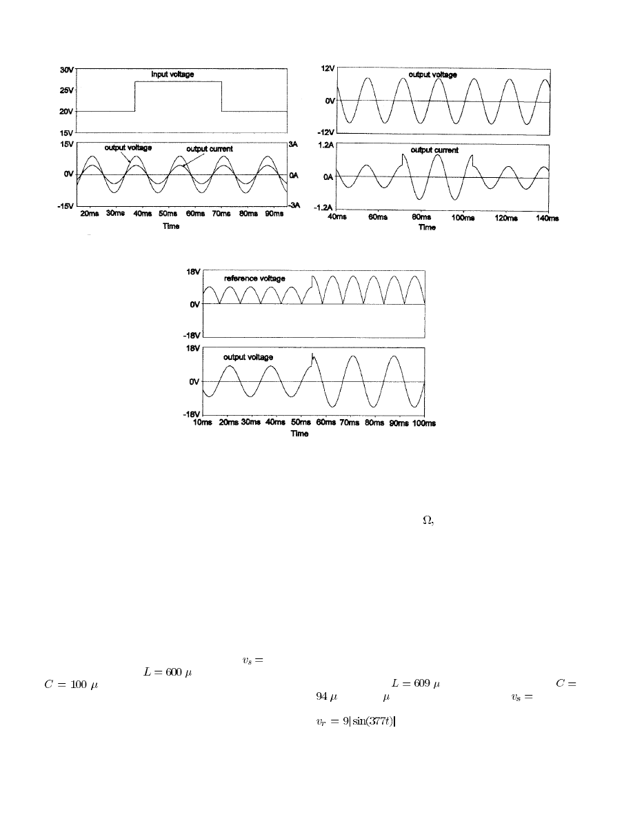
Fig. 8.
Computer simulation of the dc-to-ac inverter with nonlinear robust controller. (a) Effect of the input voltage step changes on the output voltage. (b)
Effect of the output load step changes on the output voltage. (c) Response of the output voltage to a step change of the reference signal.
The result of (6) means that the closed-loop output voltage
of the buck converter is independent of the supply voltage and
the load current. In other words, the averaged output voltage
remains unchanged, even when there is either a supply voltage
or load current disturbance. The robust control of the output
voltage of the switch-mode inverter is, therefore, achieved.
III. S
IMULATION
R
ESULTS
The proposed switch-mode dc-to-ac inverter using a buck
converter topology with the nonlinear robust control strategy
shown in Fig. 7 is simulated using PSPICE. The parameters of
the buck converter are as follows: input voltage
20–30 V;
buck filtering inductor
H; buck filtering capacitor
F.
The effect of step changes in the supply voltage have been
analyzed for the proposed inverter. The simulated result is
shown in Fig. 8(a). This result shows that, when the supply
voltage steps from 20 to 27 V, the output voltage of the inverter
does not change.
The response of the control system to a large disturbance in
the load is also studied by simulation. The result is illustrated
in Fig. 8(b). The simulation result reveals that when the load
steps between 20 and 10
the output voltage of the inverter
under the proposed control technique is not affected by the
deviations in the load.
Finally, the response of the control system to a step change
in the reference signal is simulated. The result shown in
Fig. 8(c) demonstrates that this control system has fast dy-
namic response.
IV. E
XPERIMENTAL
R
ESULTS
To verify the theoretical analysis and simulation results,
a prototype model of the inverter shown in Fig. 7 has been
breadboarded. The proposed control strategy is implemented.
The parameters of the power converter are as follows: buck
filtering inductor
H, buck filtering capacitor
F (two 47
F in parallel), input voltage
20–30 V.
The reference voltage is a fully rectified sinusoidal waveform
V.
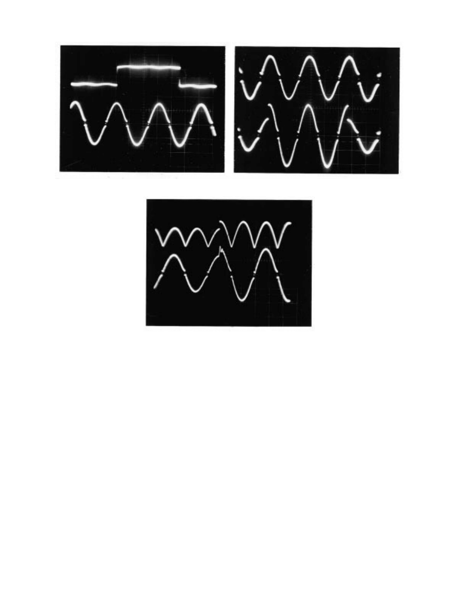
Fig. 9(a) shows the waveform of the output voltage of the
inverter when the supply voltage steps between 20 and 27
V. The oscillogram indicates that the output voltage is not
affected by the large deviations in the supply voltage.
YANG AND SEN: A NOVEL SWITCH-MODE DC-TO-AC INVERTER WITH NONLINEAR ROBUST CONTROL
607
(a)
(b)
(c)
Fig. 9.
Experimental results. (a) Effect of the input voltage step changes on the output voltage. Upper: input voltage, 5 V/div; lower: output voltage 5
V/div; time: 5 ms/div. (b) Effect of the output load step changes on the output voltage, the load resistance steps between 20 and 10
. Upper: output
voltage, 5 V/div; lower: output current, 0.4 A/div; time: 5 ms/div. (c) Dynamic response of the output voltage to a step change of the reference. Upper:
reference voltage, 5 V/div; lower: output voltage, 5 V/div; time: 5 ms/div.
Fig. 9(b) shows the effect of a large load step change on
the output voltage. The output voltage of the inverter remains
almost unchanged when the load impedance experiences a
large step change.
The response of the output voltage of the inverter to a step
change in reference voltage has been observed experimentally.
The oscillograms shown in Fig. 9(c) reveal that the output
voltage of the inverter follows the change in reference very
quickly, and only a small transient period is observed.
The above experimental results agree well with the those
derived from the computer simulation.
Some distortions appear on the output voltage in the zero-
crossing regions. This is due the discontinuous inductor current
around the output voltage zero crossing.
V. C
ONCLUSIONS
A switch-mode dc-to-ac inverter using a nonlinear robust
control technique has been presented in this paper. The analy-
sis of the control technique reveals that the output voltage of
the inverter is not affected by supply and load disturbances.
A buck converter followed by a bridge synchronizer was
used to implement the nonlinear robust control. Computer
simulations using PSPICE show that the output voltage is
immune to large deviations in the supply voltage and load
current and the system has a fast dynamic response.
A prototype of the switch-mode dc-to-ac inverter with a
buck topology has been breadboarded. The experimental re-
sults agree well with computer simulations, thus demonstrating
that the proposed robust control method can improve the
dynamic performance of the inverter.
R
EFERENCES
[1] P. C. Sen, Principles of Electric Machines and Power Electronics.
New
York: Wiley, 1989.
[2] N. Mohan, T. M. Undeland, and W. P. Robbins, Power Electronics,
Converters, Applications and Design.
New York: Wiley, 1989.
[3] J. G. Kassakian, M. F. Schlecht, and G. C. Verghese, Principles of Power
Electronics.
Reading, MA: Addison-Wesley, 1991.
[4] J. Jalade, J. Marpinard, and M. Valentin, “DC/AC high power cell
structure improves sine generator performance,” IEEE Trans. Aerosp.
Electron. Syst., vol. AES-17, pp. 373–378, May 1981.

608
IEEE TRANSACTIONS ON INDUSTRIAL ELECTRONICS, VOL. 45, NO. 4, AUGUST 1998
[5] C. Y. Hsu, “Stability analysis of a switched mode inverter using Cuk
converters,” in Conf. Rec. IEEE PESC’94, 1994, pp. 785–795.
[6] A. Capel, J. Jalade, M. Valentin, and J. C. Marpinard, “Large signal
dynamic stability analysis of synchronised current controlled modula-
tors, application to sine wave high power inverters,” in Conf. Rec. IEEE
PESC’82, 1982, pp. 101–110.
[7] J. Jalade and S. Senanyake, “Reversible power cell contributes to
efficient light weight inverter,” in Conf. Rec. IEEE PESC’86, 1986, pp.
375–380.
[8] Y. F. Liu and P. C. Sen, “A novel method to achieve zero-voltage
regulation in Buck converter,” IEEE Trans. Power Electron., vol. 10,
pp. 292–301, May 1995.
[9] R. D. Middlebrook and S. Cuk, “A general unified approach to modeling
switching power converter stages,” in Conf. Rec. IEEE PESC’76, 1976,
pp. 18–34.
[10] R. D. Middlebrook, “Modeling current-programmed Buck and Boost
converter,” IEEE Trans. Power Electron., vol. 4, pp. 36–52, Jan. 1989.
[11] D. M. Sable, R. B. Ridley, and B. H. Cho, “Comparison of performance
of single loop and current injection control for PWM converters that
operate in both continuous and discontinuous modes of operation,” IEEE
Trans. Power Electron., vol. 7, pp. 136–142, 1992.
Zaohong Yang (S’96) received the B.Sc. and M.Sc.
degrees in electrical engineering from Zhejiang Uni-
versity, Hangzhou, China, in 1984 and 1987, re-
spectively. He is currently working towards the
Ph.D. degree at Queen’s University, Kingston, Ont.,
Canada.
From 1987 to 1994, he was an Assistant Professor
at Hangzhou Institute of Electronics Engineering,
Hangzhou, China. Since 1994, he has been a Re-
search Assistant at Queen’s University. His research
interests include high-frequency power conversion,
power factor correction circuits, and high-power resonant converters for
induction heating.
Paresh C. Sen (S’67–M’67–SM’74–F’89) was born
in Chittagong, Bangladesh. He received the B.Sc.
degree (Hons.) in physics and the M.Sc. degree
(Tech.) in applied physics from the University of
Calcutta, Calcutta, India, in 1958 and 1961, respec-
tively, and the M.A.Sc. and Ph.D. degrees in elec-
trical engineering from the University of Toronto,
Toronto, Ont., Canada, in 1965 and 1967, respec-
tively.
He is currently a Professor of Electrical Engineer-
ing at Queen’s University, Kingston, Ont., Canada.
He has written more than 100 research papers in the general areas of power
electronics and drives. He is the author of two books, Thyristor DC Drives
(New York: Wiley, 1981) and Principles of Electric Machines and Power
Electronics (New York: Wiley, 1989). His fields of interest include power
electronics and drives, modern control techniques for high-performance drive
systems, and switching power supplies.
Dr. Sen has served as an Associate Editor of the IEEE T
RANSACTIONS ON
I
NDUSTRIAL
E
LECTRONICS AND
C
ONTROL
I
NSTRUMENTATION
and as Chairman
of the Technical Committees on Power Electronics (1979–1980) and Energy
Systems (1980–1982) of the IEEE Industrial Electronics Society. At present,
he is an active member of the Industrial Drives Committee and the Industrial
Power Converter Committee of the IEEE Industry Applications Society. He
received a Prize Paper Award for technical excellence from the Industrial
Drive Committee of the IEEE Industry Applications Society in 1986.
Wyszukiwarka
Podobne podstrony:
A Novel Switch mode DC to AC Inverter With Non linear Robust Control
A Novel Switch Mode Dc To Ac Inverter With Non Linear Robust Control
A Novel Switch Mode Dc To Ac Inverter With Non Linear Robust Control(1)
Dc To Ac Inverter With The 555
Modified PWM Control for the DC AC Inverter With a Non Constant Voltage Source
inverter 2002 chapter 4 DC to AC conversion inverter tutorial
Modified PWM Control for the DC AC Inverter With a Non Constant Voltage Source
Development Of High Frequency Link Direct Dc To Ac Converters For Link Direct Dc To Ac Converters Fo
12V DC to 230V AC Inverter, 12v 230v inv
(1 1)Fully Digital, Vector Controlled Pwm Vsi Fed Ac Drives With An Inverter Dead Time Compensation
A Study Of Series Resonant Dc Ac Inverter
00329965 Quasi Parallel Resonant Dc Link Inverter With Improved Pwm Capability
DC AC inverter
(1 1)Fully Digital, Vector Controlled Pwm Vsi Fed Ac Drives With An Inverter Dead Time Compensation
The Discrete Time Control of a Three Phase 4 Wire PWM Inverter with Variable DC Link Voltage and Bat
The Discrete Time Control of a Three Phase 4 Wire PWM Inverter with Variable DC Link Voltage and Bat
A Study Of Series Resonant Dc Ac Inverter
A 12kw Switching Mode Power Supply With Free Input Voltage
więcej podobnych podstron