REV. A
Information furnished by Analog Devices is believed to be accurate and
reliable. However, no responsibility is assumed by Analog Devices for its
use, nor for any infringements of patents or other rights of third parties that
may result from its use. No license is granted by implication or otherwise
under any patent or patent rights of Analog Devices.
a
ADM1810–ADM1813/ADM1815–ADM1818
One Technology Way, P.O. Box 9106, Norwood, MA 02062-9106, U.S.A.
Tel: 781/329-4700
Fax: 781/326-8703
© Analog Devices, Inc., 2002
Microprocessor
Reset Circuits
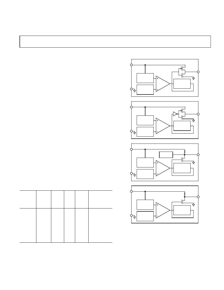
FUNCTIONAL BLOCK DIAGRAMS
V
CC
TOLERANCE
BIAS
TC
REFERENCE
150ms
DELAY
V
CC
GND
ADM1810/ADM1815
RST
V
CC
TOLERANCE
BIAS
TC
REFERENCE
150ms
DELAY
V
CC
GND
ADM1812/ADM1817
RST
V
CC
TOLERANCE
BIAS
TC
REFERENCE
150ms
DELAY
V
CC
GND
ADM1813/ADM1818
RST
RESET
MONITOR
5.5k
⍀
V
CC
TOLERANCE
BIAS
TC
REFERENCE
150ms
DELAY
V
CC
GND
ADM1811/ADM1816
RST
5.5k
⍀
FEATURES
Reliable Low-Cost Voltage Monitor with Reset Output
Supports Monitoring of Supplies Within 5%, 10%, 15%,
and 20% Tolerances
Active High and Low Push-Pull Output Choices
(ADM1810, ADM1812, ADM1815, and ADM1817)
Open Drain Output Choices (ADM1811, ADM1813,
ADM1816, and ADM1818)
Can Be Used with a Manual Push Button to Generate a
Reset (ADM1813, ADM1818)
Initialize Microprocessor Systems with Added Safety
APPLICATIONS
Microprocessor Systems
Computers
Controllers
Intelligent Instruments
Automotive Systems
GENERAL DESCRIPTION
The ADM181x range of voltage monitoring circuits can be used
in any application where an electronic system needs to be reset
when a voltage increases above or below a predetermined value.
Because of the “reset delay time” incorporated into the ADM181x
series, these devices can provide a safe startup for electronic
systems. Before a system initializes, the power supply must stabi-
lize. Using the ADM181x series ensures that there are typically
150 ms for the power supply to stabilize before the system is
reset and safe system initialization begins.
The ADM181x series of microprocessor reset circuits are available
in low-cost, space-saving SOT-23 packages.
Table I. ADM1810–ADM1813/ADM1815–ADM1818 Features
Push-
Available Trip-
V
CC
Pull/
Reset
Points (Given
Nominal Open- Active Manual as % below
5 V/3.3 V Drain
* State Reset
Nominal V
CC
)
ADM1810 5 V
PP
Low
N
5%, 10%
ADM1811 5 V
OD
Low
N
5%, 10%
ADM1812 5 V
PP
High
N
5%, 10%
ADM1813 5 V
OD
Low
Y
5%, 10%
ADM1815 3.3 V
PP
Low
N
20%
ADM1816 3.3 V
OD
Low
N
20%
ADM1817 3.3 V
PP
High
N
20%
ADM1818 3.3 V
OD
Low
Y
10%, 20%
*Open drain with internal pull-up

REV. A
–2–
ADM1810–ADM1813/ADM1815–ADM1818–SPECIFICATIONS
(T
A
= –40
ⴗC to +85ⴗC unless otherwise noted.)
Parameter
Conditions/Note
Min
Typ
Max Unit
SUPPLY
Voltage
1.2
5.5
V
Current
(ADM1810/ADM1811/ADM1813)
30
40
µA
V
CC
< 5.5 V,
RST Output Open
(ADM1812) V
CC
< 5.5 V
30
40
µA
(ADM1815/ADM1816/ADM1817/ADM1818)
28
35
µA
V
CC
< 5.5 V,
RST Output Open
OUTPUT CURRENT
@ 0.4 V, V
CC
≥ 2.7 V*
8
mA
(ADM1810/ADM1812/ADM1815/ADM1817)
350
µA
@ 2.4 V, V
CC
≥ 2.7 V
OUTPUT VOLTAGE
(ADM1810/ADM1812/ADM1815/ADM1817) V
CC
– 0.5 V
CC
– 0.1
V
@ 0
µA to 500 µA
V
CC
TRIP-POINT
ADM1810–5, ADM1810–10, ADM1811–5,
ADM1812–5, ADM1813–5
4.50
4.62
4.75 V
ADM1811–10, ADM1812–10, ADM1813–10
4.25
4.35
4.49 V
ADM1818–10
2.80
2.88
2.97 V
ADM1815–20, ADM1816–20, ADM1817–20,
ADM1818–20
2.47
2.55
2.64 V
INTERNAL PULL-UP RESISTOR
ADM1811/ADM1813/ADM1816/ADM1818
3.5
5.5
7.5
k
Ω
OUTPUT CAPACITANCE
10
pF
RESET ACTIVE TIME
100
150
300
ms
V
CC
DETECT TO
RST
Falling
(ADM1810/ADM1811/ADM1812/ADM1813)
5
10
µs
(ADM1815/ADM1816/ADM1817/ADM1818)
7
15
µs
Rising
t
R
= 5
µs
100
150
300
ms
PUSH-BUTTON DETECT TO
RST
(ADM1813/ADM1818)
1
µs
PUSH-BUTTON RESET
(ADM1818) 2.7 V
≤ V
CC
≤ 3.3 V
100
150
300
ms
(ADM1813)
100
150
300
ms
*For ADM181x-20, V
CC
= V
CCTP
, sink current reduces to 8 mA.
Specifications subject to change without notice.
REV. A
ADM1810–ADM1813/ADM1815–ADM1818
–3–
ABSOLUTE MAXIMUM RATINGS
(T
A
= 25
°C unless otherwise noted.)
V
CC
. . . . . . . . . . . . . . . . . . . . . . . . . . . . . . . . . 1.2 V to 5.5 V
Input Current . . . . . . . . . . . . . . . . . . . . . . . . . . . . . . . . 40
µA
Operating Temperature Range . . . . . . . . . . . –40
°C to +85°C
Power Dissipation, RT-3 (SOT-23) . . . . . . . . . . . . . 320 mW
Derate by 4 mW/
°C Above 70°C
JA
Thermal Impedance . . . . . . . . . . . . . . . . . . . . . . 333
°C/W
Lead Temperature (Soldering, 10 sec) . . . . . . . . . . . . 300
°C
Vapor Phase (60 sec) . . . . . . . . . . . . . . . . . . . . . . . . 215
°C
Infrared (15 sec) . . . . . . . . . . . . . . . . . . . . . . . . . . . . 220
°C
Storage Temperature Range . . . . . . . . . . . . –65
°C to +150°C
ESD Rating . . . . . . . . . . . . . . . . . . . . . . . . . . . . . . . . . . . 3 kV
PIN CONFIGURATION
TOP VIEW
(Not to Scale)
RST/RST
V
CC
GND
ADM181x
1
2
3
PIN FUNCTION DESCRIPTIONS
Pin Mnemonic Function
1
RST/RST
Reset Output.
RST/RST remains active while
V
CC
is below the reset threshold, and remains
active for 150 ms (typ) after V
CC
rises above
the reset threshold.
2
V
CC
Supply Voltage Being Monitored
3
GND
0 V. Ground Reference for All Signals.
CAUTION
ESD (electrostatic discharge) sensitive device. Electrostatic charges as high as 4000 V readily
accumulate on the human body and test equipment and can discharge without detection. Although
the ADM1810–ADM1813/ADM1815–ADM1818 features proprietary ESD protection circuitry,
permanent damage may occur on devices subjected to high-energy electrostatic discharges.
Therefore, proper ESD precautions are recommended to avoid performance degradation or loss of
functionality.
WARNING!
ESD SENSITIVE DEVICE
ORDERING GUIDE
Package
Brand
Model
*
Trip-Point
Option
Information
ADM1810-5ART-REEL
4.62 V
RT-3 (SOT-23)
MZV
ADM1810-5ART-RL7
4.62 V
RT-3 (SOT-23)
MZV
ADM1810-10ART-REEL
4.35 V
RT-3 (SOT-23)
MZT
ADM1810-10ART-RL7
4.35 V
RT-3 (SOT-23)
MZT
ADM1811-5ART-REEL
4.62 V
RT-3 (SOT-23)
M1V
ADM1811-5ART-RL7
4.62 V
RT-3 (SOT-23)
M1V
ADM1811-10ART-REEL
4.35 V
RT-3 (SOT-23)
M1T
ADM1811-10ART-RL7
4.35 V
RT-3 (SOT-23)
M1T
ADM1812-5ART-REEL
4.62 V
RT-3 (SOT-23)
MTV
ADM1812-5ART-RL7
4.62 V
RT-3 (SOT-23)
MTV
ADM1812-10ART-REEL
4.35 V
RT-3 (SOT-23)
MTT
ADM1812-10ART-RL7
4.35 V
RT-3 (SOT-23)
MTT
ADM1813-5ART-REEL
4.62 V
RT-3 (SOT-23)
M3V
ADM1813-5ART-RL7
4.62 V
RT-3 (SOT-23)
M3V
ADM1813-10ART-REEL
4.35 V
RT-3 (SOT-23)
M3T
ADM1813-10ART-RL7
4.35 V
RT-3 (SOT-23)
M3T
ADM1815-20ART-REEL
2.55 V
RT-3 (SOT-23)
M5A
ADM1815-20ART-RL7
2.55 V
RT-3 (SOT-23)
M5A
ADM1816-20ART-REEL
2.55 V
RT-3 (SOT-23)
M6A
ADM1816-20ART-RL7
2.55 V
RT-3 (SOT-23)
M6A
ADM1817-20ART-REEL
2.55 V
RT-3 (SOT-23)
M7A
ADM1817-20ART-RL7
2.55 V
RT-3 (SOT-23)
M7A
ADM1818-10ART-REEL
2.88 V
RT-3 (SOT-23)
M8E
ADM1818-10ART-RL7
2.88 V
RT-3 (SOT-23)
M8E
ADM1818-20ART-REEL
2.55 V
RT-3 (SOT-23)
M8A
ADM1818-20ART-RL7
2.55 V
RT-3 (SOT-23)
M8A
RL7 or REEL7 are in reels of 3,000 parts. REEL are in reels of 10,000 parts.
All models in bold are ex-stock. Consult factory for availability.
*Only available in reels.
REV. A
ADM1810–ADM1813/ADM1815–ADM1818
–4–
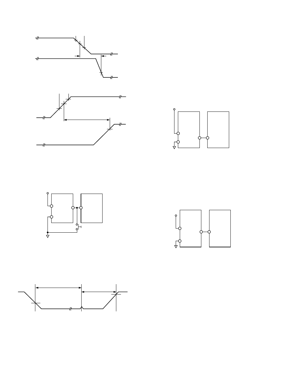
V
CC
V
CC
TRIP-POINT(MAX)
V
CC
TRIP-POINT
V
CC
TO RESET
DELAY
RST
V
CC
TRIP-POINT(MIN)
V
OL
Figure 1. Power-Down Timing Diagram
V
CC
RST
V
CC
TRIP-POINT (MAX)
V
CC
TRIP-POINT
V
CC
TRIP-POINT (MIN)
RESET ACTIVE TIMEOUT
Figure 2. Power-Up Timing Diagram
ADM1813 AND ADM1818
The ADM1813 and ADM1818 are low-cost voltage monitoring
devices featuring an open drain output and optional push-button
reset function.
ADM1813/
ADM1818
V
CC
GND
RST
V
CC
MICRO-
PROCESSOR
RESET
Figure 3. ADM1813/ADM1818 Typical Application
An optional push-button reset switch can be connected between
RST and ground. Pressing this switch will pull the reset output
low. If the push-button reset button pulls the
RST output low for
a period greater than 1
µs, then, when the reset button releases
the
RST line to float high, the RST line will stay low for a further
150 ms typical.
VOLTAGE
INPUT HIGH
PUSH-BUTTON TIME
RESET TIMEOUT
VOLTAGE
INPUT LOW
Figure 4. Push-Button Reset Timing Diagram
The ADM1818 range has options that allow the user to monitor
3.3 V supplies with 10% and 20% tolerance options; the ADM1813
range has options that allow the user to monitor 5 V supplies
with 5% and 10% tolerance options.
ADM1810, ADM1812, ADM1815, AND ADM1817
The ADM1812 is a 5 V low-cost voltage monitor with an active
high push-pull output. The ADM1812 supports a 5% or 10%
tolerance. The ADM1810 is similar to the ADM1812, except
that the ADM1810 has an active low push-pull output.
The ADM1817 is a 3.3 V voltage monitor with an active high
push-pull output. The ADM1817 supports a 20% tolerance.
The ADM1815 is similar to the ADM1817, except that the
ADM1815 has an active low push-pull output.
The ADM1810/ADM1812/ADM1815/ADM1817 can be con-
nected directly to most microprocessor reset inputs without the
need for external components.
ADM1810/
ADM1812/
ADM1815/
ADM1817
V
CC
GND
RST/RST
V
CC
MICRO-
PROCESSOR
RESET
Figure 5. ADM1810/ADM1812/ADM1815/ADM1817
Typical Application
ADM1811 AND ADM1816
The ADM1811 is a low-cost voltage monitor with an open drain
output. The ADM1811 is designed to monitor 5 V supplies. The
ADM1811 range comes in two different variants that allow the
monitoring of a 5 V supply with a tolerance of 5% or 10%. The
ADM1816 is a 3.3 V version of the ADM1811 and supports a
20% tolerance option.
ADM1811/
ADM1816
V
CC
GND
RST
V
CC
MICRO-
PROCESSOR
RESET
Figure 6. ADM1811/ADM1816 Typical Application
REV. A
ADM1810–ADM1813/ADM1815–ADM1818
–5–
OUTLINE DIMENSIONS
Dimensions shown in inches and (mm).
3-Lead Plastic Surface-Mount Package (SOT-23)
(RT-3)
0.1200 (3.048)
0.1102 (2.799)
PIN 1
0.0550 (1.397)
0.0470 (1.194)
0.0236 (0.599)
0.0177 (0.450)
0.1040 (2.642)
0.0827 (2.101)
0.0413 (1.049)
0.0374 (0.950)
0.0807 (2.050)
0.0701 (1.781)
1
2
3
SEATING
PLANE
0.0440 (1.118)
0.0320 (0.813)
0.0040 (0.102)
0.0005 (0.013)
0.0210 (0.533)
0.0146 (0.371)
0.027 (0.686)
REF
0.0059 (0.150)
0.0034 (0.086)
0.0100 (0.254)
0.0050 (0.127)

REV. A
ADM1810–ADM1813/ADM1815–ADM1818
–6–
Revision History
Location
Page
Data Sheet changed from REV. A to REV. A.
Addition of Table I . . . . . . . . . . . . . . . . . . . . . . . . . . . . . . . . . . . . . . . . . . . . . . . . . . . . . . . . . . . . . . . . . . . . . . . . . . . . . . . . . . . . . . 1
Edits to ORDERING GUIDE . . . . . . . . . . . . . . . . . . . . . . . . . . . . . . . . . . . . . . . . . . . . . . . . . . . . . . . . . . . . . . . . . . . . . . . . . . . . . . 3
Addition of new text to ADM1813 and ADM1818 section . . . . . . . . . . . . . . . . . . . . . . . . . . . . . . . . . . . . . . . . . . . . . . . . . . . . . . . . 4

–7–

–8–
C00064–0–3/02(A)
PRINTED IN U.S.A.
Wyszukiwarka
Podobne podstrony:
ADM1810 13 15 18 a
E 13 X 15 01
Części maszyn 13 - 15 BHP i ochrona środowiska, czesci maszyn
13 (15)
Ćwiczenie 13a, Patofizjologia, Ćwiczenia 13-15 (wydalniczy, nerwowy, nowotwory, toksykologia, rytmy
Metabolizm tłuszczowców, Patofizjologia, Ćwiczenia 13-15 (wydalniczy, nerwowy, nowotwory, toksykolog
13 15
biochemia str 15 18 (2)
TPL WYK 13 01 18 Tabletki, pastylki
Patofizjologia ukł oddechowego, Patofizjologia, Ćwiczenia 13-15 (wydalniczy, nerwowy, nowotwory, tok
Ćwiczenie 16, Patofizjologia, Ćwiczenia 13-15 (wydalniczy, nerwowy, nowotwory, toksykologia, rytmy b
15)18 09 Crazy?tectives praca z dialogiem VIb
Informatyka, tabela 15 ------18, Jak już wcześniej wspomniałam, na realizację zagadnień z wychowania
więcej podobnych podstron