
Features
•
High-performance, Low-power AVR
®
8-bit Microcontroller
•
Advanced RISC Architecture
– 130 Powerful Instructions – Most Single Clock Cycle Execution
– 32 x 8 General Purpose Working Registers
– Fully Static Operation
– Up to 16 MIPS Throughput at 16 MHz
– On-chip 2-cycle Multiplier
•
Nonvolatile Program and Data Memories
– 8K Bytes of In-System Self-Programmable Flash
Endurance: 10,000 Write/Erase Cycles
– Optional Boot Code Section with Independent Lock Bits
In-System Programming by On-chip Boot Program
True Read-While-Write Operation
– 512 Bytes EEPROM
Endurance: 100,000 Write/Erase Cycles
– 512 Bytes Internal SRAM
– Programming Lock for Software Security
•
Peripheral Features
– Two 8-bit Timer/Counters with Separate Prescalers and Compare Modes
– One 16-bit Timer/Counter with Separate Prescaler, Compare Mode, and Capture
Mode
– Real Time Counter with Separate Oscillator
– Four PWM Channels
– 8-channel, 10-bit ADC
8 Single-ended Channels
7 Differential Channels for TQFP Package Only
2 Differential Channels with Programmable Gain at 1x, 10x, or 200x for TQFP
Package Only
– Byte-oriented Two-wire Serial Interface
– Programmable Serial USART
– Master/Slave SPI Serial Interface
– Programmable Watchdog Timer with Separate On-chip Oscillator
– On-chip Analog Comparator
•
Special Microcontroller Features
– Power-on Reset and Programmable Brown-out Detection
– Internal Calibrated RC Oscillator
– External and Internal Interrupt Sources
– Six Sleep Modes: Idle, ADC Noise Reduction, Power-save, Power-down, Standby
and Extended Standby
•
I/O and Packages
– 32 Programmable I/O Lines
– 40-pin PDIP, 44-lead TQFP, 44-lead PLCC, and 44-pad QFN/MLF
•
Operating Voltages
– 2.7 - 5.5V for ATmega8535L
– 4.5 - 5.5V for ATmega8535
•
Speed Grades
– 0 - 8 MHz for ATmega8535L
– 0 - 16 MHz for ATmega8535
8-bit
Microcontroller
with 8K Bytes
In-System
Programmable
Flash
ATmega8535
ATmega8535L
Summary
2502KS–AVR–10/06
Note: This is a summary document. A complete document
is available on our Web site at www.atmel.com.
2
ATmega8535(L)
2502KS–AVR–10/06
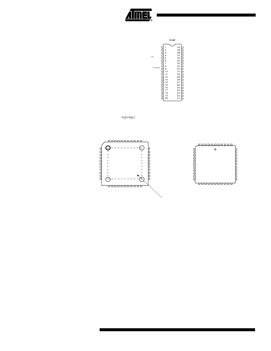
Pin Configurations
Figure 1. Pinout ATmega8535
Disclaimer
Typical values contained in this data sheet are based on simulations and characteriza-
tion of other AVR microcontrollers manufactured on the same process technology. Min
and Max values will be available after the device is characterized.
(XCK/T0) PB0
(T1) PB1
(INT2/AIN0) PB2
(OC0/AIN1) PB3
(SS) PB4
(MOSI) PB5
(MISO) PB6
(SCK) PB7
RESET
VCC
GND
XTAL2
XTAL1
(RXD) PD0
(TXD) PD1
(INT0) PD2
(INT1) PD3
(OC1B) PD4
(OC1A) PD5
(ICP1) PD6
PA0 (ADC0)
PA1 (ADC1)
PA2 (ADC2)
PA3 (ADC3)
PA4 (ADC4)
PA5 (ADC5)
PA6 (ADC6)
PA7 (ADC7)
AREF
GND
AVCC
PC7 (TOSC2)
PC6 (TOSC1)
PC5
PC4
PC3
PC2
PC1 (SDA)
PC0 (SCL)
PD7 (OC2)
1
2
3
4
5
6
7
8
9
10
11
33
32
31
30
29
28
27
26
25
24
23
(MOSI) PB5
(MISO) PB6
(SCK) PB7
RESET
VCC
GND
XTAL2
XTAL1
(RXD) PD0
(TXD) PD1
(INT0) PD2
PA4 (ADC4)
PA5 (ADC5)
PA6 (ADC6)
PA7 (ADC7)
AREF
GND
AVCC
PC7 (TOSC2)
PC6 (TOSC1)
PC5
PC4
44
43
42
41
40
39
38
37
36
35
34
12
13
14
15
16
17
18
19
20
21
22
(INT1) PD3
(OC1B) PD4
(OC1A) PD5
(ICP1) PD6
(OC2) PD7
VCC
GND
(SCL) PC0
(SDA) PC1
PC2
PC3
PB4 (SS)
PB3 (AIN1/OC0)
PB2 (AIN0/INT2)
PB1 (T1)
PB0 (XCK/T0)
GND
VCC
P
A0 (ADC0)
P
A1 (ADC1)
P
A2 (ADC2)
P
A3 (ADC3)
7
8
9
10
11
12
13
14
15
16
17
39
38
37
36
35
34
33
32
31
30
29
(MOSI) PB5
(MISO) PB6
(SCK) PB7
RESET
VCC
GND
XTAL2
XTAL1
(RXD) PD0
(TXD) PD1
(INT0) PD2
PA4 (ADC4)
PA5 (ADC5)
PA6 (ADC6)
PA7 (ADC7)
AREF
GND
AVCC
PC7 (TOSC2)
PC6 (TOSC1)
PC5
PC4
6
5
4
3
2
1
44
43
42
41
40
18
19
20
21
22
23
24
25
26
27
28
(INT1) PD3
(OC1B) PD4
(OC1A) PD5
(ICP1) PD6
(OC2) PD7
VCC
GND
(SCL) PC0
(SDA) PC1
PC2
PC3
PB4 (SS)
PB3 (AIN1/OC0)
PB2 (AIN0/INT2)
PB1 (T1)
PB0 (XCK/T0)
GND
VCC
P
A0 (ADC0)
P
A1 (ADC1)
P
A2 (ADC2)
P
A3 (ADC3)
PLCC
NOTE: MLF Bottom pad should be soldered to ground.
3
ATmega8535(L)
2502KS–AVR–10/06
Overview
The ATmega8535 is a low-power CMOS 8-bit microcontroller based on the AVR
enhanced RISC architecture. By executing instructions in a single clock cycle, the
ATmega8535 achieves throughputs approaching 1 MIPS per MHz allowing the system
designer to optimize power consumption versus processing speed.
Block Diagram
Figure 2. Block Diagram
INTERNAL
OSCILLATOR
OSCILLATOR
WATCHDOG
TIMER
MCU CTRL.
& TIMING
OSCILLATOR
TIMERS/
COUNTERS
INTERRUPT
UNIT
STACK
POINTER
EEPROM
SRAM
STATUS
REGISTER
USART
PROGRAM
COUNTER
PROGRAM
FLASH
INSTRUCTION
REGISTER
INSTRUCTION
DECODER
PROGRAMMING
LOGIC
SPI
ADC
INTERFACE
COMP.
INTERFACE
PORTA DRIVERS/BUFFERS
PORTA DIGITAL INTERFACE
GENERAL
PURPOSE
REGISTERS
X
Y
Z
ALU
+
-
PORTC DRIVERS/BUFFERS
PORTC DIGITAL INTERFACE
PORTB DIGITAL INTERFACE
PORTB DRIVERS/BUFFERS
PORTD DIGITAL INTERFACE
PORTD DRIVERS/BUFFERS
XTAL1
XTAL2
RESET
CONTROL
LINES
V
CC
GND
MUX &
ADC
AREF
PA0 - PA7
PC0 - PC7
PD0 - PD7
PB0 - PB7
AVR CPU
TWI
AVCC
INTERNAL
CALIBRATED
OSCILLATOR

4
ATmega8535(L)
2502KS–AVR–10/06
The AVR core combines a rich instruction set with 32 general purpose working registers.
All 32 registers are directly connected to the Arithmetic Logic Unit (ALU), allowing two
independent registers to be accessed in one single instruction executed in one clock
cycle. The resulting architecture is more code efficient while achieving throughputs up to
ten times faster than conventional CISC microcontrollers.
The ATmega8535 provides the following features: 8K bytes of In-System Programmable
Flash with Read-While-Write capabilities, 512 bytes EEPROM, 512 bytes SRAM, 32
general purpose I/O lines, 32 general purpose working registers, three flexible
Timer/Counters with compare modes, internal and external interrupts, a serial program-
mable USART, a byte oriented Two-wire Serial Interface, an 8-channel, 10-bit ADC with
optional differential input stage with programmable gain in TQFP package, a program-
mable Watchdog Timer with Internal Oscillator, an SPI serial port, and six software
selectable power saving modes. The Idle mode stops the CPU while allowing the
SRAM, Timer/Counters, SPI port, and interrupt system to continue functioning. The
Power-down mode saves the register contents but freezes the Oscillator, disabling all
other chip functions until the next interrupt or Hardware Reset. In Power-save mode, the
asynchronous timer continues to run, allowing the user to maintain a timer base while
the rest of the device is sleeping. The ADC Noise Reduction mode stops the CPU and
all I/O modules except asynchronous timer and ADC, to minimize switching noise during
ADC conversions. In Standby mode, the crystal/resonator Oscillator is running while the
rest of the device is sleeping. This allows very fast start-up combined with low-power
consumption. In Extended Standby mode, both the main Oscillator and the asynchro-
nous timer continue to run.
The device is manufactured using Atmel’s high density nonvolatile memory technology.
The On-chip ISP Flash allows the program memory to be reprogrammed In-System
through an SPI serial interface, by a conventional nonvolatile memory programmer, or
by an On-chip Boot program running on the AVR core. The boot program can use any
interface to download the application program in the Application Flash memory. Soft-
ware in the Boot Flash section will continue to run while the Application Flash section is
updated, providing true Read-While-Write operation. By combining an 8-bit RISC CPU
with In-System Self-Programmable Flash on a monolithic chip, the Atmel ATmega8535
is a powerful microcontroller that provides a highly flexible and cost effective solution to
many embedded control applications.
The ATmega8535 AVR is supported with a full suite of program and system develop-
ment tools including: C compilers, macro assemblers, program debugger/simulators, In-
Circuit Emulators, and evaluation kits.
AT90S8535 Compatibility
The ATmega8535 provides all the features of the AT90S8535. In addition, several new
features are added. The ATmega8535 is backward compatible with AT90S8535 in most
cases. However, some incompatibilities between the two microcontrollers exist. To
solve this problem, an AT90S8535 compatibility mode can be selected by programming
the S8535C fuse. ATmega8535 is pin compatible with AT90S8535, and can replace the
AT90S8535 on current Printed Circuit Boards. However, the location of fuse bits and the
electrical characteristics differs between the two devices.
AT90S8535 Compatibility
Mode
Programming the S8535C fuse will change the following functionality:
•
The timed sequence for changing the Watchdog Time-out period is disabled. See
“Timed Sequences for Changing the Configuration of the Watchdog Timer” on page
45 for details.
•
The double buffering of the USART Receive Register is disabled. See “AVR USART
vs. AVR UART – Compatibility” on page 146 for details.

5
ATmega8535(L)
2502KS–AVR–10/06
Pin Descriptions
V
CC
Digital supply voltage.
GND
Ground.
Port A (PA7..PA0)
Port A serves as the analog inputs to the A/D Converter.
Port A also serves as an 8-bit bi-directional I/O port, if the A/D Converter is not used.
Port pins can provide internal pull-up resistors (selected for each bit). The Port A output
buffers have symmetrical drive characteristics with both high sink and source capability.
When pins PA0 to PA7 are used as inputs and are externally pulled low, they will source
current if the internal pull-up resistors are activated. The Port A pins are tri-stated when
a reset condition becomes active, even if the clock is not running.
Port B (PB7..PB0)
Port B is an 8-bit bi-directional I/O port with internal pull-up resistors (selected for each
bit). The Port B output buffers have symmetrical drive characteristics with both high sink
and source capability. As inputs, Port B pins that are externally pulled low will source
current if the pull-up resistors are activated. The Port B pins are tri-stated when a reset
condition becomes active, even if the clock is not running.
Port B also serves the functions of various special features of the ATmega8535 as listed
on page 60.
Port C (PC7..PC0)
Port C is an 8-bit bi-directional I/O port with internal pull-up resistors (selected for each
bit). The Port C output buffers have symmetrical drive characteristics with both high sink
and source capability. As inputs, Port C pins that are externally pulled low will source
current if the pull-up resistors are activated. The Port C pins are tri-stated when a reset
condition becomes active, even if the clock is not running.
Port D (PD7..PD0)
Port D is an 8-bit bi-directional I/O port with internal pull-up resistors (selected for each
bit). The Port D output buffers have symmetrical drive characteristics with both high sink
and source capability. As inputs, Port D pins that are externally pulled low will source
current if the pull-up resistors are activated. The Port D pins are tri-stated when a reset
condition becomes active, even if the clock is not running.
Port D also serves the functions of various special features of the ATmega8535 as listed
on page 64.
RESET
Reset input. A low level on this pin for longer than the minimum pulse length will gener-
ate a reset, even if the clock is not running. The minimum pulse length is given in Table
15 on page 37. Shorter pulses are not guaranteed to generate a reset.
XTAL1
Input to the inverting Oscillator amplifier and input to the internal clock operating circuit.
XTAL2
Output from the inverting Oscillator amplifier.
AVCC
AVCC is the supply voltage pin for Port A and the A/D Converter. It should be externally
connected to V
CC
, even if the ADC is not used. If the ADC is used, it should be con-
nected to V
CC
through a low-pass filter.
AREF
AREF is the analog reference pin for the A/D Converter.

6
ATmega8535(L)
2502KS–AVR–10/06
Resources
A comprehensive set of development tools, application notes and datasheets are avail-
able for download on http://www.atmel.com/avr.

7
ATmega8535(L)
2502KS–AVR–10/06
About Code
Examples
This documentation contains simple code examples that briefly show how to use various
parts of the device. These code examples assume that the part specific header file is
included before compilation. Be aware that not all C compiler vendors include bit defini-
tions in the header files and interrupt handling in C is compiler dependent. Please
confirm with the C Compiler documentation for more details.
8
ATmega8535(L)
2502KS–AVR–10/06
.
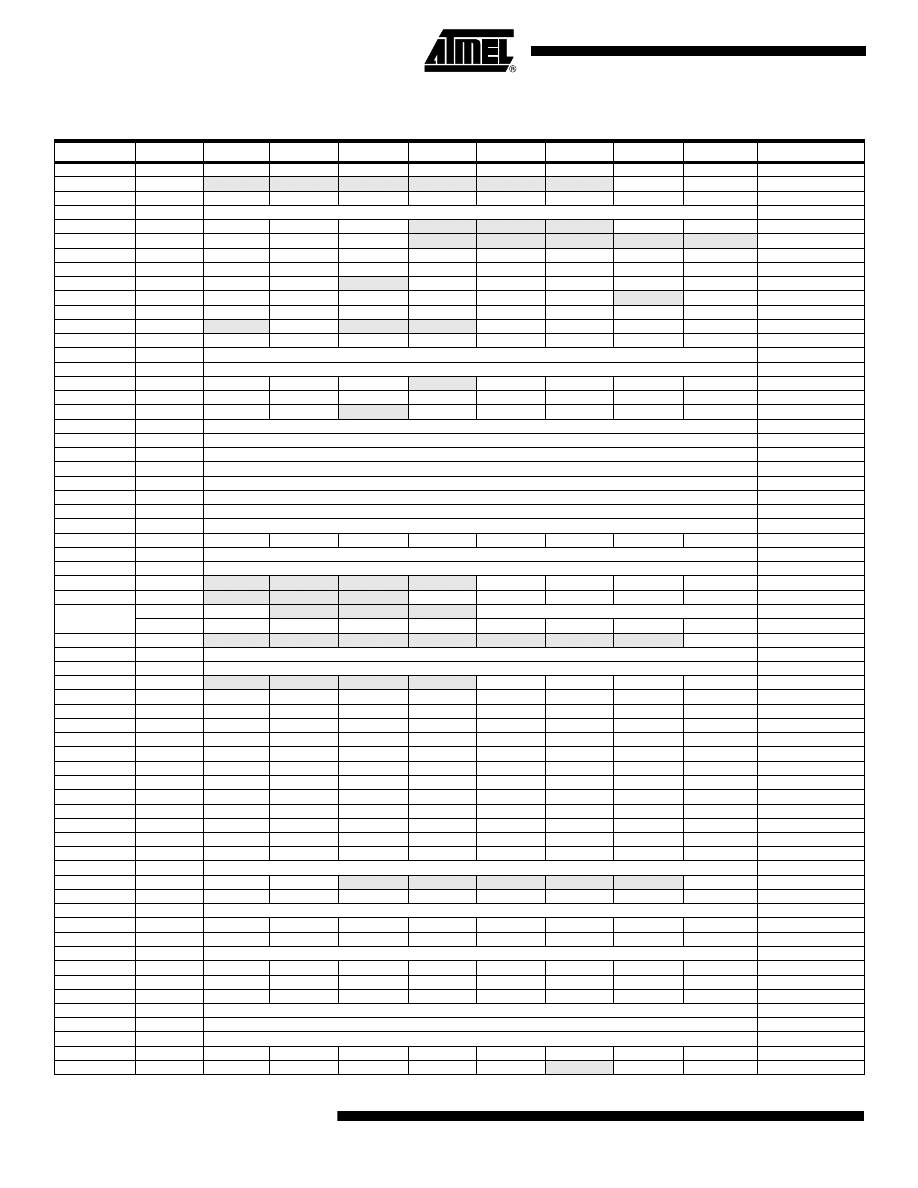
Register Summary
Address
Name
Bit 7
Bit 6
Bit 5
Bit 4
Bit 3
Bit 2
Bit 1
Bit 0
Page
0x3F (0x5F)
SREG
I
T
H
S
V
N
Z
C
10
0x3E (0x5E)
SPH
–
–
–
–
–
–
SP9
SP8
12
0x3D (0x5D)
SPL
SP7
SP6
SP5
SP4
SP3
SP2
SP1
SP0
12
0x3C (0x5C)
OCR0
Timer/Counter0 Output Compare Register
85
0x3B (0x5B)
GICR
INT1
INT0
INT2
–
–
–
IVSEL
IVCE
49, 69
0x3A (0x5A)
GIFR
INTF1
INTF0
INTF2
–
–
–
–
–
70
0x39 (0x59)
TIMSK
OCIE2
TOIE2
TICIE1
OCIE1A
OCIE1B
TOIE1
OCIE0
TOIE0
85, 115, 133
0x38 (0x58)
TIFR
OCF2
TOV2
ICF1
OCF1A
OCF1B
TOV1
OCF0
TOV0
86, 116, 134
0x37 (0x57)
SPMCR
SPMIE
RWWSB
–
RWWSRE
BLBSET
PGWRT
PGERS
SPMEN
228
0x36 (0x56)
TWCR
TWINT
TWEA
TWSTA
TWSTO
TWWC
TWEN
–
TWIE
181
0x35 (0x55)
MCUCR
SM2
SE
SM1
SM0
ISC11
ISC10
ISC01
ISC00
32, 68
0x34 (0x54)
MCUCSR
–
ISC2
–
–
WDRF
BORF
EXTRF
PORF
40, 69
0x33 (0x53)
TCCR0
FOC0
WGM00
COM01
COM00
WGM01
CS02
CS01
CS00
83
0x32 (0x52)
TCNT0
Timer/Counter0 (8 Bits)
85
0x31 (0x51)
OSCCAL
Oscillator Calibration Register
30
0x30 (0x50)
SFIOR
ADTS2
ADTS1
ADTS0
–
ACME
PUD
PSR2
PSR10
59,88,135,203,223
0x2F (0x4F)
TCCR1A
COM1A1
COM1A0
COM1B1
COM1B0
FOC1A
FOC1B
WGM11
WGM10
110
0x2E (0x4E)
TCCR1B
ICNC1
ICES1
–
WGM13
WGM12
CS12
CS11
CS10
113
0x2D (0x4D)
TCNT1H
Timer/Counter1 – Counter Register High Byte
114
0x2C (0x4C)
TCNT1L
Timer/Counter1 – Counter Register Low Byte
114
0x2B (0x4B)
OCR1AH
Timer/Counter1 – Output Compare Register A High Byte
114
0x2A (0x4A)
OCR1AL
Timer/Counter1 – Output Compare Register A Low Byte
114
0x29 (0x49)
OCR1BH
Timer/Counter1 – Output Compare Register B High Byte
114
0x28 (0x48)
OCR1BL
Timer/Counter1 – Output Compare Register B Low Byte
114
0x27 (0x47)
ICR1H
Timer/Counter1 – Input Capture Register High Byte
114
0x26 (0x46)
ICR1L
Timer/Counter1 – Input Capture Register Low Byte
114
0x25 (0x45)
TCCR2
FOC2
WGM20
COM21
COM20
WGM21
CS22
CS21
CS20
128
0x24 (0x44)
TCNT2
Timer/Counter2 (8 Bits)
130
0x23 (0x43)
OCR2
Timer/Counter2 Output Compare Register
131
0x22 (0x42)
ASSR
–
–
–
–
AS2
TCN2UB
OCR2UB
TCR2UB
131
0x21 (0x41)
WDTCR
–
–
–
WDCE
WDE
WDP2
WDP1
WDP0
42
0x20
(0x40)
UBRRH
URSEL
–
–
–
UBRR[11:8]
169
UCSRC
URSEL
UMSEL
UPM1
UPM0
USBS
UCSZ1
UCSZ0
UCPOL
167
0x1F (0x3F)
EEARH
–
–
–
–
–
–
–
EEAR8
19
0x1E (0x3E)
EEARL
EEPROM Address Register Low Byte
19
0x1D (0x3D)
EEDR
EEPROM Data Register
19
0x1C (0x3C)
EECR
–
–
–
–
EERIE
EEMWE
EEWE
EERE
19
0x1B (0x3B)
PORTA
PORTA7
PORTA6
PORTA5
PORTA4
PORTA3
PORTA2
PORTA1
PORTA0
66
0x1A (0x3A)
DDRA
DDA7
DDA6
DDA5
DDA4
DDA3
DDA2
DDA1
DDA0
66
0x19 (0x39)
PINA
PINA7
PINA6
PINA5
PINA4
PINA3
PINA2
PINA1
PINA0
66
0x18 (0x38)
PORTB
PORTB7
PORTB6
PORTB5
PORTB4
PORTB3
PORTB2
PORTB1
PORTB0
66
0x17 (0x37)
DDRB
DDB7
DDB6
DDB5
DDB4
DDB3
DDB2
DDB1
DDB0
66
0x16 (0x36)
PINB
PINB7
PINB6
PINB5
PINB4
PINB3
PINB2
PINB1
PINB0
67
0x15 (0x35)
PORTC
PORTC7
PORTC6
PORTC5
PORTC4
PORTC3
PORTC2
PORTC1
PORTC0
67
0x14 (0x34)
DDRC
DDC7
DDC6
DDC5
DDC4
DDC3
DDC2
DDC1
DDC0
67
0x13 (0x33)
PINC
PINC7
PINC6
PINC5
PINC4
PINC3
PINC2
PINC1
PINC0
67
0x12 (0x32)
PORTD
PORTD7
PORTD6
PORTD5
PORTD4
PORTD3
PORTD2
PORTD1
PORTD0
67
0x11 (0x31)
DDRD
DDD7
DDD6
DDD5
DDD4
DDD3
DDD2
DDD1
DDD0
67
0x10 (0x30)
PIND
PIND7
PIND6
PIND5
PIND4
PIND3
PIND2
PIND1
PIND0
67
0x0F (0x2F)
SPDR
SPI Data Register
143
0x0E (0x2E)
SPSR
SPIF
WCOL
–
–
–
–
–
SPI2X
143
0x0D (0x2D)
SPCR
SPIE
SPE
DORD
MSTR
CPOL
CPHA
SPR1
SPR0
141
0x0C (0x2C)
UDR
USART I/O Data Register
164
0x0B (0x2B)
UCSRA
RXC
TXC
UDRE
FE
DOR
PE
U2X
MPCM
165
0x0A (0x2A)
UCSRB
RXCIE
TXCIE
UDRIE
RXEN
TXEN
UCSZ2
RXB8
TXB8
166
0x09 (0x29)
UBRRL
USART Baud Rate Register Low Byte
169
0x08 (0x28)
ACSR
ACD
ACBG
ACO
ACI
ACIE
ACIC
ACIS1
ACIS0
203
0x07 (0x27)
ADMUX
REFS1
REFS0
ADLAR
MUX4
MUX3
MUX2
MUX1
MUX0
219
0x06 (0x26)
ADCSRA
ADEN
ADSC
ADATE
ADIF
ADIE
ADPS2
ADPS1
ADPS0
221
0x05 (0x25)
ADCH
ADC Data Register High Byte
222
0x04 (0x24)
ADCL
ADC Data Register Low Byte
222
0x03 (0x23)
TWDR
Two-wire Serial Interface Data Register
183
0x02 (0x22)
TWAR
TWA6
TWA5
TWA4
TWA3
TWA2
TWA1
TWA0
TWGCE
183
0x01 (0x21)
TWSR
TWS7
TWS6
TWS5
TWS4
TWS3
–
TWPS1
TWPS0
183

9
ATmega8535(L)
2502KS–AVR–10/06
Notes:
1. Refer to the USART description for details on how to access UBRRH and UCSRC.
2. For compatibility with future devices, reserved bits should be written to zero if accessed. Reserved I/O memory addresses
should never be written.
3. Some of the status flags are cleared by writing a logical one to them. Note that the CBI and SBI instructions will operate on
all bits in the I/O Register, writing a one back into any flag read as set, thus clearing the flag. The CBI and SBI instructions
work with registers 0x00 to 0x1F only.
0x00 (0x20)
TWBR
Two-wire Serial Interface Bit Rate Register
181
Register Summary (Continued)
Address
Name
Bit 7
Bit 6
Bit 5
Bit 4
Bit 3
Bit 2
Bit 1
Bit 0
Page
10
ATmega8535(L)
2502KS–AVR–10/06
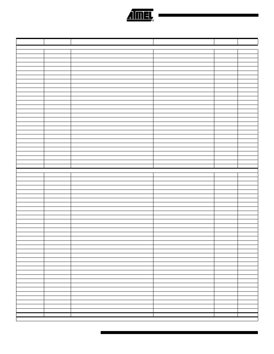
Instruction Set Summary
Mnemonics
Operands
Description
Operation
Flags
#Clocks
ARITHMETIC AND LOGIC INSTRUCTIONS
ADD
Rd, Rr
Add two Registers
Rd
← Rd + Rr
Z,C,N,V,H
1
ADC
Rd, Rr
Add with Carry two Registers
Rd
← Rd + Rr + C
Z,C,N,V,H
1
ADIW
Rdl,K
Add Immediate to Word
Rdh:Rdl
← Rdh:Rdl + K
Z,C,N,V,S
2
SUB
Rd, Rr
Subtract two Registers
Rd
← Rd - Rr
Z,C,N,V,H
1
SUBI
Rd, K
Subtract Constant from Register
Rd
← Rd - K
Z,C,N,V,H
1
SBC
Rd, Rr
Subtract with Carry two Registers
Rd
← Rd - Rr - C
Z,C,N,V,H
1
SBCI
Rd, K
Subtract with Carry Constant from Reg.
Rd
← Rd - K - C
Z,C,N,V,H
1
SBIW
Rdl,K
Subtract Immediate from Word
Rdh:Rdl
← Rdh:Rdl - K
Z,C,N,V,S
2
AND
Rd, Rr
Logical AND Registers
Rd
← Rd • Rr
Z,N,V
1
ANDI
Rd, K
Logical AND Register and Constant
Rd
← Rd • K
Z,N,V
1
OR
Rd, Rr
Logical OR Registers
Rd
← Rd v Rr
Z,N,V
1
ORI
Rd, K
Logical OR Register and Constant
Rd
← Rd v K
Z,N,V
1
EOR
Rd, Rr
Exclusive OR Registers
Rd
← Rd ⊕ Rr
Z,N,V
1
COM
Rd
One’s Complement
Rd
← 0xFF − Rd
Z,C,N,V
1
NEG
Rd
Two’s Complement
Rd
← 0x00 − Rd
Z,C,N,V,H
1
SBR
Rd,K
Set Bit(s) in Register
Rd
← Rd v K
Z,N,V
1
CBR
Rd,K
Clear Bit(s) in Register
Rd
← Rd • (0xFF - K)
Z,N,V
1
INC
Rd
Increment
Rd
← Rd + 1
Z,N,V
1
DEC
Rd
Decrement
Rd
← Rd − 1
Z,N,V
1
TST
Rd
Test for Zero or Minus
Rd
← Rd • Rd
Z,N,V
1
CLR
Rd
Clear Register
Rd
← Rd ⊕ Rd
Z,N,V
1
SER
Rd
Set Register
Rd
← 0xFF
None
1
MUL
Rd, Rr
Multiply Unsigned
R1:R0
← Rd x Rr
Z,C
2
MULS
Rd, Rr
Multiply Signed
R1:R0
← Rd x Rr
Z,C
2
MULSU
Rd, Rr
Multiply Signed with Unsigned
R1:R0
← Rd x Rr
Z,C
2
FMUL
Rd, Rr
Fractional Multiply Unsigned
R1:R0
← (Rd x Rr)
<< 1
Z,C
2
FMULS
Rd, Rr
Fractional Multiply Signed
R1:R0
← (Rd x Rr)
<< 1
Z,C
2
FMULSU
Rd, Rr
Fractional Multiply Signed with Unsigned
R1:R0
← (Rd x Rr)
<< 1
Z,C
2
BRANCH INSTRUCTIONS
RJMP
k
Relative Jump
PC
← PC + k + 1
None
2
IJMP
Indirect Jump to (Z)
PC
← Z
None
2
RCALL
k
Relative Subroutine Call
PC
← PC + k + 1
None
3
ICALL
Indirect Call to (Z)
PC
← Z
None
3
RET
Subroutine Return
PC
← STACK
None
4
RETI
Interrupt Return
PC
← STACK
I
4
CPSE
Rd,Rr
Compare, Skip if Equal
if (Rd = Rr) PC
← PC + 2 or 3
None
1 / 2 / 3
CP
Rd,Rr
Compare
Rd
− Rr
Z, N,V,C,H
1
CPC
Rd,Rr
Compare with Carry
Rd
− Rr − C
Z, N,V,C,H
1
CPI
Rd,K
Compare Register with Immediate
Rd
− K
Z, N,V,C,H
1
SBRC
Rr, b
Skip if Bit in Register Cleared
if (Rr(b)=0) PC
← PC + 2 or 3
None
1 / 2 / 3
SBRS
Rr, b
Skip if Bit in Register is Set
if (Rr(b)=1) PC
← PC + 2 or 3
None
1 / 2 / 3
SBIC
P, b
Skip if Bit in I/O Register Cleared
if (P(b)=0) PC
← PC + 2 or 3
None
1 / 2 / 3
SBIS
P, b
Skip if Bit in I/O Register is Set
if (P(b)=1) PC
← PC + 2 or 3
None
1 / 2 / 3
BRBS
s, k
Branch if Status Flag Set
if (SREG(s) = 1) then PC
←PC+k + 1
None
1 / 2
BRBC
s, k
Branch if Status Flag Cleared
if (SREG(s) = 0) then PC
←PC+k + 1
None
1 / 2
BREQ
k
Branch if Equal
if (Z = 1) then PC
← PC + k + 1
None
1 / 2
BRNE
k
Branch if Not Equal
if (Z = 0) then PC
← PC + k + 1
None
1 / 2
BRCS
k
Branch if Carry Set
if (C = 1) then PC
← PC + k + 1
None
1 / 2
BRCC
k
Branch if Carry Cleared
if (C = 0) then PC
← PC + k + 1
None
1 / 2
BRSH
k
Branch if Same or Higher
if (C = 0) then PC
← PC + k + 1
None
1 / 2
BRLO
k
Branch if Lower
if (C = 1) then PC
← PC + k + 1
None
1 / 2
BRMI
k
Branch if Minus
if (N = 1) then PC
← PC + k + 1
None
1 / 2
BRPL
k
Branch if Plus
if (N = 0) then PC
← PC + k + 1
None
1 / 2
BRGE
k
Branch if Greater or Equal, Signed
if (N
⊕ V= 0) then PC ← PC + k + 1
None
1 / 2
BRLT
k
Branch if Less Than Zero, Signed
if (N
⊕ V= 1) then PC ← PC + k + 1
None
1 / 2
BRHS
k
Branch if Half Carry Flag Set
if (H = 1) then PC
← PC + k + 1
None
1 / 2
BRHC
k
Branch if Half Carry Flag Cleared
if (H = 0) then PC
← PC + k + 1
None
1 / 2
BRTS
k
Branch if T Flag Set
if (T = 1) then PC
← PC + k + 1
None
1 / 2
BRTC
k
Branch if T Flag Cleared
if (T = 0) then PC
← PC + k + 1
None
1 / 2
BRVS
k
Branch if Overflow Flag is Set
if (V = 1) then PC
← PC + k + 1
None
1 / 2
BRVC
k
Branch if Overflow Flag is Cleared
if (V = 0) then PC
← PC + k + 1
None
1 / 2
BRIE
k
Branch if Interrupt Enabled
if ( I = 1) then PC
← PC + k + 1
None
1 / 2
BRID
k
Branch if Interrupt Disabled
if ( I = 0) then PC
← PC + k + 1
None
1 / 2
DATA TRANSFER INSTRUCTIONS
11
ATmega8535(L)
2502KS–AVR–10/06
MOV
Rd, Rr
Move Between Registers
Rd
← Rr
None
1
MOVW
Rd, Rr
Copy Register Word
Rd+1:Rd
← Rr+1:Rr
None
1
LDI
Rd, K
Load Immediate
Rd
← K
None
1
LD
Rd, X
Load Indirect
Rd
← (X)
None
2
LD
Rd, X+
Load Indirect and Post-Inc.
Rd
← (X), X ← X + 1
None
2
LD
Rd, - X
Load Indirect and Pre-Dec.
X
← X - 1, Rd ← (X)
None
2
LD
Rd, Y
Load Indirect
Rd
← (Y)
None
2
LD
Rd, Y+
Load Indirect and Post-Inc.
Rd
← (Y), Y ← Y + 1
None
2
LD
Rd, - Y
Load Indirect and Pre-Dec.
Y
← Y - 1, Rd ← (Y)
None
2
LDD
Rd,Y+q
Load Indirect with Displacement
Rd
← (Y + q)
None
2
LD
Rd, Z
Load Indirect
Rd
← (Z)
None
2
LD
Rd, Z+
Load Indirect and Post-Inc.
Rd
← (Z), Z ← Z+1
None
2
LD
Rd, -Z
Load Indirect and Pre-Dec.
Z
← Z - 1, Rd ← (Z)
None
2
LDD
Rd, Z+q
Load Indirect with Displacement
Rd
← (Z + q)
None
2
LDS
Rd, k
Load Direct from SRAM
Rd
← (k)
None
2
ST
X, Rr
Store Indirect
(X)
← Rr
None
2
ST
X+, Rr
Store Indirect and Post-Inc.
(X)
← Rr, X ← X + 1
None
2
ST
- X, Rr
Store Indirect and Pre-Dec.
X
← X - 1, (X) ← Rr
None
2
ST
Y, Rr
Store Indirect
(Y)
← Rr
None
2
ST
Y+, Rr
Store Indirect and Post-Inc.
(Y)
← Rr, Y ← Y + 1
None
2
ST
- Y, Rr
Store Indirect and Pre-Dec.
Y
← Y - 1, (Y) ← Rr
None
2
STD
Y+q,Rr
Store Indirect with Displacement
(Y + q)
← Rr
None
2
ST
Z, Rr
Store Indirect
(Z)
← Rr
None
2
ST
Z+, Rr
Store Indirect and Post-Inc.
(Z)
← Rr, Z ← Z + 1
None
2
ST
-Z, Rr
Store Indirect and Pre-Dec.
Z
← Z - 1, (Z) ← Rr
None
2
STD
Z+q,Rr
Store Indirect with Displacement
(Z + q)
← Rr
None
2
STS
k, Rr
Store Direct to SRAM
(k)
← Rr
None
2
LPM
Load Program Memory
R0
← (Z)
None
3
LPM
Rd, Z
Load Program Memory
Rd
← (Z)
None
3
LPM
Rd, Z+
Load Program Memory and Post-Inc
Rd
← (Z), Z ← Z+1
None
3
SPM
Store Program Memory
(Z)
← R1:R0
None
-
IN
Rd, P
In Port
Rd
← P
None
1
OUT
P, Rr
Out Port
P
← Rr
None
1
PUSH
Rr
Push Register on Stack
STACK
← Rr
None
2
POP
Rd
Pop Register from Stack
Rd
← STACK
None
2
BIT AND BIT-TEST INSTRUCTIONS
SBI
P,b
Set Bit in I/O Register
I/O(P,b)
← 1
None
2
CBI
P,b
Clear Bit in I/O Register
I/O(P,b)
← 0
None
2
LSL
Rd
Logical Shift Left
Rd(n+1)
← Rd(n), Rd(0) ← 0
Z,C,N,V
1
LSR
Rd
Logical Shift Right
Rd(n)
← Rd(n+1), Rd(7) ← 0
Z,C,N,V
1
ROL
Rd
Rotate Left Through Carry
Rd(0)
←C,Rd(n+1)← Rd(n),C←Rd(7)
Z,C,N,V
1
ROR
Rd
Rotate Right Through Carry
Rd(7)
←C,Rd(n)← Rd(n+1),C←Rd(0)
Z,C,N,V
1
ASR
Rd
Arithmetic Shift Right
Rd(n)
← Rd(n+1), n=0..6
Z,C,N,V
1
SWAP
Rd
Swap Nibbles
Rd(3..0)
←Rd(7..4),Rd(7..4)←Rd(3..0)
None
1
BSET
s
Flag Set
SREG(s)
← 1
SREG(s)
1
BCLR
s
Flag Clear
SREG(s)
← 0
SREG(s)
1
BST
Rr, b
Bit Store from Register to T
T
← Rr(b)
T
1
BLD
Rd, b
Bit load from T to Register
Rd(b)
← T
None
1
SEC
Set Carry
C
← 1
C
1
CLC
Clear Carry
C
← 0
C
1
SEN
Set Negative Flag
N
← 1
N
1
CLN
Clear Negative Flag
N
← 0
N
1
SEZ
Set Zero Flag
Z
← 1
Z
1
CLZ
Clear Zero Flag
Z
← 0
Z
1
SEI
Global Interrupt Enable
I
← 1
I
1
CLI
Global Interrupt Disable
I
← 0
I
1
SES
Set Signed Test Flag
S
← 1
S
1
CLS
Clear Signed Test Flag
S
← 0
S
1
SEV
Set Twos Complement Overflow.
V
← 1
V
1
CLV
Clear Twos Complement Overflow
V
← 0
V
1
SET
Set T in SREG
T
← 1
T
1
CLT
Clear T in SREG
T
← 0
T
1
SEH
Set Half Carry Flag in SREG
H
← 1
H
1
CLH
Clear Half Carry Flag in SREG
H
← 0
H
1
MCU CONTROL INSTRUCTIONS
NOP
No Operation
None
1
Mnemonics
Operands
Description
Operation
Flags
#Clocks

12
ATmega8535(L)
2502KS–AVR–10/06
SLEEP
Sleep
(see specific descr. for Sleep function)
None
1
WDR
Watchdog Reset
(see specific descr. for WDR/Timer)
None
1
BREAK
Break
For On-chip Debug Only
None
N/A
Mnemonics
Operands
Description
Operation
Flags
#Clocks

13
ATmega8535(L)
2502KS–AVR–10/06
Ordering Information
Note:
1. This device can also be supplied in wafer form. Please contact your local Atmel sales office for detailed ordering information
and minimum quantities..
2. Pb-free packaging alternative, complies to the European Directive for Restriction of Hazardous Substances (RoHS direc-
tive).Also Halide free and fully Green.
Speed (MHz)
Power Supply
Ordering Code
Package
Operation Range
8
2.7 - 5.5V
ATmega8535L-8AC
ATmega8535L-8PC
ATmega8535L-8JC
ATmega8535L-8MC
44A
40P6
44J
44M1
Commercial
(
0
°C to 70°C)
ATmega8535L-8AI
ATmega8535L-8PI
ATmega8535L-8JI
ATmega8535L-8MI
ATmega8535L-8AU
ATmega8535L-8PU
ATmega8535L-8JU
ATmega8535L-8MU
44A
40P6
44J
44M1
44A
40P6
44J
44M1
Industrial
(-4
0
°C to 85°C)
16
4.5 - 5.5V
ATmega8535-16AC
ATmega8535-16PC
ATmega8535-16JC
ATmega8535-16MC
44A
40P6
44J
44M1
Commercial
(
0
°C to 70°C)
ATmega8535-16AI
ATmega8535-16PI
ATmega8535-16JI
ATmega8535-16MI
ATmega8535-16AU
ATmega8535-16PU
ATmega8535-16JU
ATmega8535-16MU
44A
40P6
44J
44M1
44A
40P6
44J
44M1
Industrial
(-4
0
°C to 85°C)
Package Type
44A
44-lead, Thin (1.0 mm) Plastic Gull Wing Quad Flat Package (TQFP)
40P6
40-pin, 0.600” Wide, Plastic Dual Inline Package (PDIP)
44J
44-lead, Plastic J-leaded Chip Carrier (PLCC)
44M1-A
44-pad, 7 x 7 x 1.0 mm body, lead pitch 0.50 mm, Quad Flat No-Lead/Micro Lead Frame Package (QFN/MLF)
14
ATmega8535(L)
2502KS–AVR–10/06
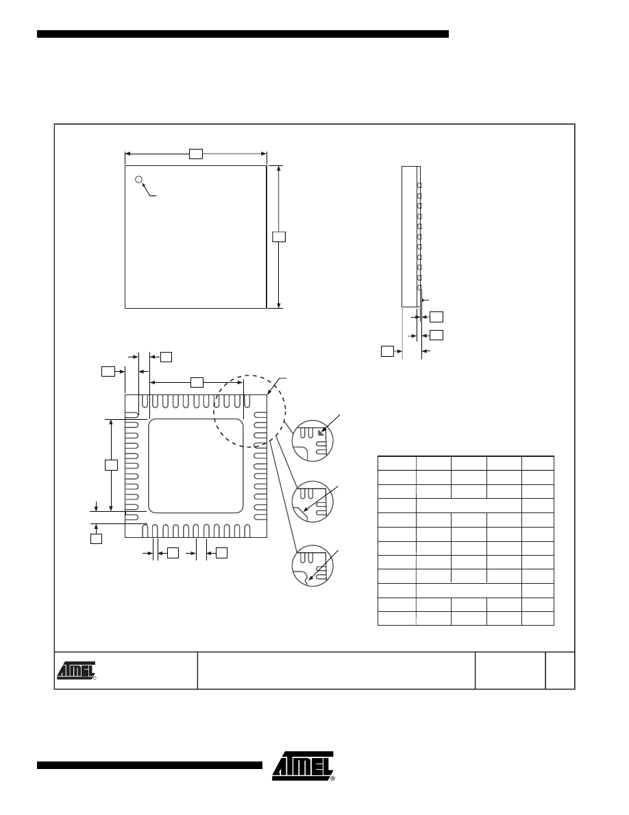
Packaging Information
44A
2325 Orchard Parkway
San Jose, CA 95131
TITLE
DRAWING NO.
R
REV.
44A, 44-lead, 10 x 10 mm Body Size, 1.0 mm Body Thickness,
0.8 mm Lead Pitch, Thin Profile Plastic Quad Flat Package (TQFP)
B
44A
10/5/2001
PIN 1 IDENTIFIER
0˚~7˚
PIN 1
L
C
A1
A2
A
D1
D
e
E1
E
B
COMMON DIMENSIONS
(Unit of Measure = mm)
SYMBOL
MIN
NOM
MAX
NOTE
Notes:
1. This package conforms to JEDEC reference MS-026, Variation ACB.
2. Dimensions D1 and E1 do not include mold protrusion. Allowable
protrusion is 0.25 mm per side. Dimensions D1 and E1 are maximum
plastic body size dimensions including mold mismatch.
3. Lead coplanarity is 0.10 mm maximum.
A
–
–
1.20
A1
0.05
–
0.15
A2
0.95
1.00
1.05
D
11.75
12.00
12.25
D1
9.90
10.00
10.10
Note 2
E
11.75
12.00
12.25
E1
9.90
10.00
10.10
Note 2
B 0.30
–
0.45
C
0.09
–
0.20
L
0.45
–
0.75
e
0.80 TYP
15
ATmega8535(L)
2502KS–AVR–10/06
40P6
2325 Orchard Parkway
San Jose, CA 95131
TITLE
DRAWING NO.
R
REV.
40P6, 40-lead (0.600"/15.24 mm Wide) Plastic Dual
Inline Package (PDIP)
B
40P6
09/28/01
PIN
1
E1
A1
B
REF
E
B1
C
L
SEATING PLANE
A
0º ~ 15º
D
e
eB
COMMON DIMENSIONS
(Unit of Measure = mm)
SYMBOL
MIN
NOM
MAX
NOTE
A
–
–
4.826
A1
0.381
–
–
D
52.070
–
52.578
Note 2
E
15.240
–
15.875
E1
13.462
–
13.970
Note 2
B
0.356
–
0.559
B1
1.041
–
1.651
L
3.048
–
3.556
C
0.203
–
0.381
eB
15.494
–
17.526
e
2.540 TYP
Notes:
1. This package conforms to JEDEC reference MS-011, Variation AC.
2. Dimensions D and E1 do not include mold Flash or Protrusion.
Mold Flash or Protrusion shall not exceed 0.25 mm (0.010").
16
ATmega8535(L)
2502KS–AVR–10/06
44J
Notes:
1. This package conforms to JEDEC reference MS-018, Variation AC.
2. Dimensions D1 and E1 do not include mold protrusion.
Allowable protrusion is .010"(0.254 mm) per side. Dimension D1
and E1 include mold mismatch and are measured at the extreme
material condition at the upper or lower parting line.
3. Lead coplanarity is 0.004" (0.102 mm) maximum.
A
4.191
–
4.572
A1
2.286
–
3.048
A2
0.508
–
–
D
17.399
–
17.653
D1
16.510
–
16.662
Note 2
E
17.399
–
17.653
E1
16.510
–
16.662
Note 2
D2/E2
14.986
–
16.002
B
0.660
–
0.813
B1
0.330
–
0.533
e
1.270 TYP
COMMON DIMENSIONS
(Unit of Measure = mm)
SYMBOL
MIN
NOM
MAX
NOTE
1.14(0.045) X 45˚
PIN NO. 1
IDENTIFIER
1.14(0.045) X 45˚
0.51(0.020)MAX
0.318(0.0125)
0.191(0.0075)
A2
45˚ MAX (3X)
A
A1
B1
D2/E2
B
e
E1
E
D1
D
44J, 44-lead, Plastic J-leaded Chip Carrier (PLCC)
B
44J
10/04/01
2325 Orchard Parkway
San Jose, CA 95131
TITLE
DRAWING NO.
R
REV.
17
ATmega8535(L)
2502KS–AVR–10/06
44M1-A
2325 Orchard Parkway
San Jose, CA 95131
TITLE
DRAWING NO.
R
REV.
44M1, 44-pad, 7 x 7 x 1.0 mm Body, Lead Pitch 0.50 mm,
G
44M1
5/27/06
COMMON DIMENSIONS
(Unit of Measure = mm)
SYMBOL
MIN
NOM
MAX
NOTE
A
0.80 0.90 1.00
A1
–
0.02
0.05
A3
0.25
REF
b 0.18
0.23
0.30
D
D2
5.00
5.20
5.40
6.90
7.00
7.10
6.90
7.00
7.10
E
E2
5.00
5.20
5.40
e
0.50 BSC
L
0.59
0.64
0.69
K
0.20
0.26
0.41
Note: JEDEC Standard MO-220, Fig. 1 (SAW Singulation) VKKD-3.
TOP VIEW
SIDE VIEW
BOTTOM VIEW
D
E
Marked Pin# 1 ID
E2
D2
b
e
Pin #1 Corner
L
A1
A3
A
SEATING PLANE
Pin #1
Triangle
Pin #1
Chamfer
(C 0.30)
Option A
Option B
Pin #1
Notch
(0.20 R)
Option C
K
K
1
2
3
5.20 mm Exposed Pad, Micro Lead Frame Package (MLF)

18
ATmega8535(L)
2502KS–AVR–10/06
Errata
The revision letter refer to the device revision.
ATmega8535
Rev. A and B
•
First Analog Comparator conversion may be delayed
•
Asynchronous Oscillator does not stop in Power-down
1.
First Analog Comparator conversion may be delayed
If the device is powered by a slow rising V
CC
, the first Analog Comparator conver-
sion will take longer than expected on some devices.
Problem Fix/Workaround
When the device has been powered or reset, disable then enable the Analog Com-
parator before the first conversion.
2.
Asynchronous Oscillator does not stop in Power-down
The asynchronous oscillator does not stop when entering Power-down mode. This
leads to higher power consumption than expected.
Problem Fix/Workaround
Manually disable the asynchronous timer before entering Power-down.

19
ATmega8535(L)
2502KS–AVR–10/06
Datasheet Revision
History
Please note that the referring page numbers in this section are referring to this docu-
ment. The referring revision in this section are referring to the document revision.
Changes from Rev.
2502J- 08/06 to Rev.
2502K- 10/06
1.
Updated TOP/BOTTOM description for all Timer/Counters Fast PWM mode.
2.
Updated “Errata” on page 18.
Changes from Rev.
2502I- 06/06 to Rev.
2502J- 08/06
1.
Updated “Ordering Information” on page 13.
Changes from Rev.
2502H- 04/06 to Rev.
2502I- 06/06
1.
Updated code example “USART Initialization” on page 150.
Changes from Rev.
2502G- 04/05 to Rev.
2502H- 04/06
1.
2.
Updated Table 7 on page 29, Table 17 on page 42 and Table 111 on page 258.
3.
Updated “Serial Peripheral Interface – SPI” on page 136.
4.
Updated note in “Bit Rate Generator Unit” on page 180.
Changes from Rev.
2502F- 06/04 to Rev.
2502G- 04/05
1.
Removed “Preliminary” and TBD’s.
2.
Updated Table 37 on page 69 and Table 113 on page 261.
3.
Updated “Electrical Characteristics” on page 255.
4.
Updated “Ordering Information” on page 13.
Changes from Rev.
2502E-12/03 to Rev.
2502G-06/04
1.
MLF-package alternative changed to “Quad Flat No-Lead/Micro Lead Frame
Package QFN/MLF”.
Changes from Rev.
2502E-12/03 to Rev.
2502F-06/04
1.
Updated “Reset Characteristics” on page 37.
2.
Updated SPH in “Stack Pointer” on page 12.
3.
Updated C code in “USART Initialization” on page 150.
4.
Updated “Errata” on page 18.
Changes from Rev.
2502D-09/03 to Rev.
2502E-12/03
1.
Updated “Calibrated Internal RC Oscillator” on page 29.
2.
Added section “Errata” on page 18.

20
ATmega8535(L)
2502KS–AVR–10/06
Changes from Rev.
2502C-04/03 to Rev.
2502D-09/03
1.
Removed “Advance Information” and some TBD’s from the datasheet.
2.
Added note to “Pinout ATmega8535” on page 2.
3.
Updated “Reset Characteristics” on page 37.
4.
Updated “Absolute Maximum Ratings” and “DC Characteristics” in “Electrical
Characteristics” on page 255.
5.
Updated Table 111 on page 258.
6.
Updated “ADC Characteristics” on page 263.
7.
Updated “ATmega8535 Typical Characteristics” on page 266.
8.
Removed CALL and JMP instructions from code examples and “Instruction
Set Summary” on page 10.
Changes from Rev.
2502B-09/02 to Rev.
2502C-04/03
1.
Updated “Packaging Information” on page 14.
2.
Updated Figure 1 on page 2, Figure 84 on page 179, Figure 85 on page 185,
Figure 87 on page 191, Figure 98 on page 207.
3.
Added the section “EEPROM Write During Power-down Sleep Mode” on page
22.
4.
Removed the references to the application notes “Multi-purpose Oscillator”
and “32 kHz Crystal Oscillator”, which do not exist.
5.
Updated code examples on page 44.
6.
Removed ADHSM bit.
7.
Renamed Port D pin ICP to ICP1. See “Alternate Functions of Port D” on page
64.
8.
Added information about PWM symmetry for Timer 0 on page 79 and Timer 2
on page 126.
9.
Updated Table 68 on page 169, Table 75 on page 190, Table 76 on page 193,
Table 77 on page 196, Table 108 on page 253, Table 113 on page 261.
10. Updated description on “Bit 5 – TWSTA: TWI START Condition Bit” on page
182.
11. Updated the description in “Filling the Temporary Buffer (Page Loading)” and
“Performing a Page Write” on page 231.
12. Removed the section description in “SPI Serial Programming Characteristics”
on page 254.
13. Updated “Electrical Characteristics” on page 255.

21
ATmega8535(L)
2502KS–AVR–10/06
14. Updated “ADC Characteristics” on page 263.
14. Updated “Register Summary” on page 8.
15. Various Timer 1 corrections.
16. Added WD_FUSE period in Table 108 on page 253.
Changes from Rev.
2502A-06/02 to Rev.
2502B-09/02
1.
Canged the Endurance on the Flash to 10,000 Write/Erase Cycles.

2502KS–AVR–10/06
Disclaimer: The information in this document is provided in connection with Atmel products. No license, express or implied, by estoppel or otherwise, to any
intellectual property right is granted by this document or in connection with the sale of Atmel products. EXCEPT AS SET FORTH IN ATMEL’S TERMS AND CONDI-
TIONS OF SALE LOCATED ON ATMEL’S WEB SITE, ATMEL ASSUMES NO LIABILITY WHATSOEVER AND DISCLAIMS ANY EXPRESS, IMPLIED OR STATUTORY
WARRANTY RELATING TO ITS PRODUCTS INCLUDING, BUT NOT LIMITED TO, THE IMPLIED WARRANTY OF MERCHANTABILITY, FITNESS FOR A PARTICULAR
PURPOSE, OR NON-INFRINGEMENT. IN NO EVENT SHALL ATMEL BE LIABLE FOR ANY DIRECT, INDIRECT, CONSEQUENTIAL, PUNITIVE, SPECIAL OR INCIDEN-
TAL DAMAGES (INCLUDING, WITHOUT LIMITATION, DAMAGES FOR LOSS OF PROFITS, BUSINESS INTERRUPTION, OR LOSS OF INFORMATION) ARISING OUT
OF THE USE OR INABILITY TO USE THIS DOCUMENT, EVEN IF ATMEL HAS BEEN ADVISED OF THE POSSIBILITY OF SUCH DAMAGES. Atmel makes no
representations or warranties with respect to the accuracy or completeness of the contents of this document and reserves the right to make changes to specifications
and product descriptions at any time without notice. Atmel does not make any commitment to update the information contained herein. Atmel’s products are not
intended, authorized, or warranted for use as components in applications intended to support or sustain life.
Atmel Corporation
Atmel Operations
2325 Orchard Parkway
San Jose, CA 95131, USA
Tel: 1(408) 441-0311
Fax: 1(408) 487-2600
Regional Headquarters
Europe
Atmel Sarl
Route des Arsenaux 41
Case Postale 80
CH-1705 Fribourg
Switzerland
Tel: (41) 26-426-5555
Fax: (41) 26-426-5500
Asia
Room 1219
Chinachem Golden Plaza
77 Mody Road Tsimshatsui
East Kowloon
Hong Kong
Tel: (852) 2721-9778
Fax: (852) 2722-1369
Japan
9F, Tonetsu Shinkawa Bldg.
1-24-8 Shinkawa
Chuo-ku, Tokyo 104-0033
Japan
Tel: (81) 3-3523-3551
Fax: (81) 3-3523-7581
Memory
2325 Orchard Parkway
San Jose, CA 95131, USA
Tel: 1(408) 441-0311
Fax: 1(408) 436-4314
Microcontrollers
2325 Orchard Parkway
San Jose, CA 95131, USA
Tel: 1(408) 441-0311
Fax: 1(408) 436-4314
La Chantrerie
BP 70602
44306 Nantes Cedex 3, France
Tel: (33) 2-40-18-18-18
Fax: (33) 2-40-18-19-60
ASIC/ASSP/Smart Cards
Zone Industrielle
13106 Rousset Cedex, France
Tel: (33) 4-42-53-60-00
Fax: (33) 4-42-53-60-01
1150 East Cheyenne Mtn. Blvd.
Colorado Springs, CO 80906, USA
Tel: 1(719) 576-3300
Fax: 1(719) 540-1759
Scottish Enterprise Technology Park
Maxwell Building
East Kilbride G75 0QR, Scotland
Tel: (44) 1355-803-000
Fax: (44) 1355-242-743
RF/Automotive
Theresienstrasse 2
Postfach 3535
74025 Heilbronn, Germany
Tel: (49) 71-31-67-0
Fax: (49) 71-31-67-2340
1150 East Cheyenne Mtn. Blvd.
Colorado Springs, CO 80906, USA
Tel: 1(719) 576-3300
Fax: 1(719) 540-1759
Biometrics/Imaging/Hi-Rel MPU/
High Speed Converters/RF Datacom
Avenue de Rochepleine
BP 123
38521 Saint-Egreve Cedex, France
Tel: (33) 4-76-58-30-00
Fax: (33) 4-76-58-34-80
Literature Requests
www.atmel.com/literature
© 2006 Atmel Corporation. All rights reserved. Atmel
®
, logo and combinations thereof, Everywhere You Are
®
, AVR
®
, and others are the trade-
marks or registered trademarks of Atmel Corporation or its subsidiaries. Other terms and product names may be trademarks of others.
Document Outline
- Features
- Pin Configurations
- Overview
- Resources
- About Code Examples
- Register Summary
- Instruction Set Summary
- Ordering Information
- Packaging Information
- Errata
- Datasheet Revision History
- Changes from Rev. 2502J- 08/06 to Rev. 2502K- 10/06
- Changes from Rev. 2502I- 06/06 to Rev. 2502J- 08/06
- Changes from Rev. 2502H- 04/06 to Rev. 2502I- 06/06
- Changes from Rev. 2502G- 04/05 to Rev. 2502H- 04/06
- Changes from Rev. 2502F- 06/04 to Rev. 2502G- 04/05
- Changes from Rev. 2502E-12/03 to Rev. 2502G-06/04
- Changes from Rev. 2502E-12/03 to Rev. 2502F-06/04
- Changes from Rev. 2502D-09/03 to Rev. 2502E-12/03
- Changes from Rev. 2502C-04/03 to Rev. 2502D-09/03
- Changes from Rev. 2502B-09/02 to Rev. 2502C-04/03
- Changes from Rev. 2502A-06/02 to Rev. 2502B-09/02
Wyszukiwarka
Podobne podstrony:
atmega128 id 71652 Nieznany
ATmega3290 id 71659 Nieznany (2)
AtMega32 AVRISP id 71658 Nieznany
atmega16 pl id 71656 Nieznany
ATMEGA64L8AU ATMEL id 71661 Nieznany (2)
Abolicja podatkowa id 50334 Nieznany (2)
4 LIDER MENEDZER id 37733 Nieznany (2)
katechezy MB id 233498 Nieznany
metro sciaga id 296943 Nieznany
perf id 354744 Nieznany
interbase id 92028 Nieznany
Mbaku id 289860 Nieznany
Probiotyki antybiotyki id 66316 Nieznany
miedziowanie cz 2 id 113259 Nieznany
LTC1729 id 273494 Nieznany
D11B7AOver0400 id 130434 Nieznany
więcej podobnych podstron