
THE I
2
C-BUS SPECIFICATION
VERSION 2.1
JANUARY 2000
document order number: 9398 393 40011

2
Philips Semiconductors
The I
2
C-bus specification
CONTENTS
1
PREFACE . . . . . . . . . . . . . . . . . . . . . . . . . . . 3
1.1
Version 1.0 - 1992. . . . . . . . . . . . . . . . . . . . 3
1.2
Version 2.0 - 198. . . . . . . . . . . . . . . . . . . . . 3
1.3
Version 2.1 - 1999. . . . . . . . . . . . . . . . . . . . 3
1.4
Purchase of Philips I
2
C-bus components . . 3
2
THE I
2
C-BUS BENEFITS DESIGNERS
AND MANUFACTURERS . . . . . . . . . . . . . . . 4
2.1
Designer benefits . . . . . . . . . . . . . . . . . . . . 4
2.2
Manufacturer benefits . . . . . . . . . . . . . . . . . 6
3
INTRODUCTION TO THE I
2
C-BUS
SPECIFICATION . . . . . . . . . . . . . . . . . . . . . 6
4
THE I
2
C-BUS CONCEPT . . . . . . . . . . . . . . . 6
5
GENERAL CHARACTERISTICS . . . . . . . . . 8
6
BIT TRANSFER . . . . . . . . . . . . . . . . . . . . . . 8
6.1
Data validity . . . . . . . . . . . . . . . . . . . . . . . . 8
6.2
START and STOP conditions . . . . . . . . . . . 9
7
TRANSFERRING DATA . . . . . . . . . . . . . . . 10
7.1
Byte format . . . . . . . . . . . . . . . . . . . . . . . . 10
7.2
Acknowledge. . . . . . . . . . . . . . . . . . . . . . . 10
8
ARBITRATION AND CLOCK
GENERATION . . . . . . . . . . . . . . . . . . . . . . 11
8.1
Synchronization . . . . . . . . . . . . . . . . . . . . 11
8.2
Arbitration . . . . . . . . . . . . . . . . . . . . . . . . . 12
8.3
Use of the clock synchronizing
mechanism as a handshake . . . . . . . . . . . 13
9
FORMATS WITH 7-BIT ADDRESSES . . . . 13
10
7-BIT ADDRESSING . . . . . . . . . . . . . . . . . 15
10.1
Definition of bits in the first byte . . . . . . . . 15
10.1.1
General call address . . . . . . . . . . . . . . . . . 16
10.1.2
START byte . . . . . . . . . . . . . . . . . . . . . . . 17
10.1.3
CBUS compatibility . . . . . . . . . . . . . . . . . . 18
11
EXTENSIONS TO THE STANDARD-
MODE I
2
C-BUS SPECIFICATION . . . . . . . 19
12
FAST-MODE . . . . . . . . . . . . . . . . . . . . . . . . 19
13
Hs-MODE . . . . . . . . . . . . . . . . . . . . . . . . . . 20
13.1
High speed transfer. . . . . . . . . . . . . . . . . . 20
13.2
Serial data transfer format in Hs-mode . . . 21
13.3
Switching from F/S- to Hs-mode and
back . . . . . . . . . . . . . . . . . . . . . . . . . . . . . 23
13.4
Hs-mode devices at lower speed modes . . 24
13.5
Mixed speed modes on one serial bus
system . . . . . . . . . . . . . . . . . . . . . . . . . . . . 24
13.5.1
F/S-mode transfer in a mixed-speed bus
system . . . . . . . . . . . . . . . . . . . . . . . . . . . . 25
13.5.2
Hs-mode transfer in a mixed-speed bus
system . . . . . . . . . . . . . . . . . . . . . . . . . . . . 25
13.5.3
Timing requirements for the bridge in a
mixed-speed bus system . . . . . . . . . . . . . . 27
14
10-BIT ADDRESSING . . . . . . . . . . . . . . . . 27
14.1
Definition of bits in the first two bytes. . . . . 27
14.2
Formats with 10-bit addresses. . . . . . . . . . 27
14.3
General call address and start byte with
10-bit addressing . . . . . . . . . . . . . . . . . . . . 30
15
ELECTRICAL SPECIFICATIONS
AND TIMING FOR I/O STAGES
AND BUS LINES . . . . . . . . . . . . . . . . . . . . 30
15.1
Standard- and Fast-mode devices. . . . . . . 30
15.2
Hs-mode devices . . . . . . . . . . . . . . . . . . . . 34
16
ELECTRICAL CONNECTIONS OF
I
2
C-BUS DEVICES TO THE BUS LINES . 37
16.1
Maximum and minimum values of
resistors R
p
and R
s
for Standard-mode
I
2
C-bus devices . . . . . . . . . . . . . . . . . . . . . 39
17
APPLICATION INFORMATION . . . . . . . . . 41
17.1
Slope-controlled output stages of
Fast-mode I
2
C-bus devices . . . . . . . . . . . . 41
17.2
Switched pull-up circuit for Fast-mode
I
2
C-bus devices . . . . . . . . . . . . . . . . . . . . . 41
17.3
Wiring pattern of the bus lines . . . . . . . . . . 42
17.4
Maximum and minimum values of
resistors R
p
and R
s
for Fast-mode
I
2
C-bus devices . . . . . . . . . . . . . . . . . . . . . 42
17.5
Maximum and minimum values of
resistors R
p
and R
s
for Hs-mode
I
2
C-bus devices . . . . . . . . . . . . . . . . . . . . . 42
18
BI-DIRECTIONAL LEVEL SHIFTER
FOR F/S-MODE I
2
C-BUS SYSTEMS . . . . 42
18.1
Connecting devices with different
logic levels . . . . . . . . . . . . . . . . . . . . . . . . . 43
18.1.1
Operation of the level shifter . . . . . . . . . . . 44
19
DEVELOPMENT TOOLS AVAILABLE
FROM PHILIPS . . . . . . . . . . . . . . . . . . . . . 45
20
SUPPORT LITERATURE . . . . . . . . . . . . . 46
3
Philips Semiconductors
The I
2
C-bus specification
1
PREFACE
1.1
Version 1.0 - 1992
This version of the 1992 I
2
C-bus specification includes the
following modifications:
•
Programming of a slave address by software has been
omitted. The realization of this feature is rather
complicated and has not been used.
•
The “low-speed mode” has been omitted. This mode is,
in fact, a subset of the total I
2
C-bus specification and
need not be specified explicitly.
•
The Fast-mode is added. This allows a fourfold increase
of the bit rate up to 400 kbit/s. Fast-mode devices are
downwards compatible i.e. they can be used in a 0 to
100 kbit/s I
2
C-bus system.
•
10-bit addressing is added. This allows 1024 additional
slave addresses.
•
Slope control and input filtering for Fast-mode devices is
specified to improve the EMC behaviour.
NOTE: Neither the 100 kbit/s I
2
C-bus system nor the
100 kbit/s devices have been changed.
1.2
Version 2.0 - 1998
The I
2
C-bus has become a de facto world standard that is
now implemented in over 1000 different ICs and licensed
to more than 50 companies. Many of today’s applications,
however, require higher bus speeds and lower supply
voltages. This updated version of the I
2
C-bus specification
meets those requirements and includes the following
modifications:
•
The High-speed mode (Hs-mode) is added. This allows
an increase in the bit rate up to 3.4 Mbit/s. Hs-mode
devices can be mixed with Fast- and Standard-mode
devices on the one I
2
C-bus system with bit rates from 0
to 3.4 Mbit/s.
•
The low output level and hysteresis of devices with a
supply voltage of 2 V and below has been adapted to
meet the required noise margins and to remain
compatible with higher supply voltage devices.
•
The 0.6 V at 6 mA requirement for the output stages of
Fast-mode devices has been omitted.
•
The fixed input levels for new devices are replaced by
bus voltage-related levels.
•
Application information for bi-directional level shifter is
added.
1.3
Version 2.1 - 2000
Version 2.1 of the I
2
C-bus specification includes the
following minor modifications:
•
After a repeated START condition in Hs-mode, it is
possible to stretch the clock signal SCLH (see
Section 13.2 and Figs 22, 25 and 32).
•
Some timing parameters in Hs-mode have been relaxed
(see Tables 6 and 7).
1.4
Purchase of Philips I
2
C-bus components
Purchase of Philips I
2
C components conveys a license under the Philips’ I
2
C patent to use the
components in the I
2
C system provided the system conforms to the I
2
C specification defined by
Philips.

4
Philips Semiconductors
The I
2
C-bus specification
2
THE I
2
C-BUS BENEFITS DESIGNERS AND
MANUFACTURERS
In consumer electronics, telecommunications and
industrial electronics, there are often many similarities
between seemingly unrelated designs. For example,
nearly every system includes:
•
Some intelligent control, usually a single-chip
microcontroller
•
General-purpose circuits like LCD drivers, remote I/O
ports, RAM, EEPROM, or data converters
•
Application-oriented circuits such as digital tuning and
signal processing circuits for radio and video systems, or
DTMF generators for telephones with tone dialling.
To exploit these similarities to the benefit of both systems
designers and equipment manufacturers, as well as to
maximize hardware efficiency and circuit simplicity, Philips
developed a simple bi-directional 2-wire bus for efficient
inter-IC control. This bus is called the Inter IC or I
2
C-bus.
At present, Philips’ IC range includes more than 150
CMOS and bipolar I
2
C-bus compatible types for
performing functions in all three of the previously
mentioned categories. All I
2
C-bus compatible devices
incorporate an on-chip interface which allows them to
communicate directly with each other via the I
2
C-bus. This
design concept solves the many interfacing problems
encountered when designing digital control circuits.
Here are some of the features of the I
2
C-bus:
•
Only two bus lines are required; a serial data line (SDA)
and a serial clock line (SCL)
•
Each device connected to the bus is software
addressable by a unique address and simple
master/slave relationships exist at all times; masters can
operate as master-transmitters or as master-receivers
•
It’s a true multi-master bus including collision detection
and arbitration to prevent data corruption if two or more
masters simultaneously initiate data transfer
•
Serial, 8-bit oriented, bi-directional data transfers can be
made at up to 100 kbit/s in the Standard-mode, up to
400 kbit/s in the Fast-mode, or up to 3.4 Mbit/s in the
High-speed mode
•
On-chip filtering rejects spikes on the bus data line to
preserve data integrity
•
The number of ICs that can be connected to the same
bus is limited only by a maximum bus capacitance of
400 pF.
Figure 1 shows two examples of I
2
C-bus applications.
2.1
Designer benefits
I
2
C-bus compatible ICs allow a system design to rapidly
progress directly from a functional block diagram to a
prototype. Moreover, since they ‘clip’ directly onto the
I
2
C-bus without any additional external interfacing, they
allow a prototype system to be modified or upgraded
simply by ‘clipping’ or ‘unclipping’ ICs to or from the bus.
Here are some of the features of I
2
C-bus compatible ICs
which are particularly attractive to designers:
•
Functional blocks on the block diagram correspond with
the actual ICs; designs proceed rapidly from block
diagram to final schematic.
•
No need to design bus interfaces because the I
2
C-bus
interface is already integrated on-chip.
•
Integrated addressing and data-transfer protocol allow
systems to be completely software-defined
•
The same IC types can often be used in many different
applications
•
Design-time reduces as designers quickly become
familiar with the frequently used functional blocks
represented by I
2
C-bus compatible ICs
•
ICs can be added to or removed from a system without
affecting any other circuits on the bus
•
Fault diagnosis and debugging are simple; malfunctions
can be immediately traced
•
Software development time can be reduced by
assembling a library of reusable software modules.
In addition to these advantages, the CMOS ICs in the
I
2
C-bus compatible range offer designers special features
which are particularly attractive for portable equipment and
battery-backed systems.
They all have:
•
Extremely low current consumption
•
High noise immunity
•
Wide supply voltage range
•
Wide operating temperature range.
5
Philips Semiconductors
The I
2
C-bus specification
Fig.1 Two examples of I
2
C-bus applications: (a) a high performance highly-integrated TV set
(b) DECT cordless phone base-station.
handbook, full pagewidth
SDA
SCL
MICRO-
CONTROLLER
PCB83C528
PLL
SYNTHESIZER
TSA5512
NON-VOLATILE
MEMORY
PCF8582E
STEREO / DUAL
SOUND
DECODER
TDA9840
HI-FI
AUDIO
PROCESSOR
TDA9860
SINGLE-CHIP
TEXT
SAA52XX
M/S COLOUR
DECODER
TDA9160A
PICTURE
SIGNAL
IMPROVEMENT
TDA4670
VIDEO
PROCESSOR
TDA4685
ON-SCREEN
DISPLAY
PCA8510
(a)
MSB575
SDA
SCL
LINE
INTERFACE
PCA1070
BURST MODE
CONTROLLER
PCD5042
ADPCM
PCD5032
(b)
DTMF
GENERATOR
PCD3311
MICRO-
CONTROLLER
P80CLXXX

6
Philips Semiconductors
The I
2
C-bus specification
2.2
Manufacturer benefits
I
2
C-bus compatible ICs don’t only assist designers, they
also give a wide range of benefits to equipment
manufacturers because:
•
The simple 2-wire serial I
2
C-bus minimizes
interconnections so ICs have fewer pins and there are
not so many PCB tracks; result - smaller and less
expensive PCBs
•
The completely integrated I
2
C-bus protocol eliminates
the need for address decoders and other ‘glue logic’
•
The multi-master capability of the I
2
C-bus allows rapid
testing and alignment of end-user equipment via
external connections to an assembly-line
•
The availability of I
2
C-bus compatible ICs in SO (small
outline), VSO (very small outline) as well as DIL
packages reduces space requirements even more.
These are just some of the benefits. In addition, I
2
C-bus
compatible ICs increase system design flexibility by
allowing simple construction of equipment variants and
easy upgrading to keep designs up-to-date. In this way, an
entire family of equipment can be developed around a
basic model. Upgrades for new equipment, or
enhanced-feature models (i.e. extended memory, remote
control, etc.) can then be produced simply by clipping the
appropriate ICs onto the bus. If a larger ROM is needed,
it’s simply a matter of selecting a micro-controller with a
larger ROM from our comprehensive range. As new ICs
supersede older ones, it’s easy to add new features to
equipment or to increase its performance by simply
unclipping the outdated IC from the bus and clipping on its
successor.
3
INTRODUCTION TO THE I
2
C-BUS SPECIFICATION
For 8-bit oriented digital control applications, such as those
requiring microcontrollers, certain design criteria can be
established:
•
A complete system usually consists of at least one
microcontroller and other peripheral devices such as
memories and I/O expanders
•
The cost of connecting the various devices within the
system must be minimized
•
A system that performs a control function doesn’t
require high-speed data transfer
•
Overall efficiency depends on the devices chosen and
the nature of the interconnecting bus structure.
To produce a system to satisfy these criteria, a serial bus
structure is needed. Although serial buses don’t have the
throughput capability of parallel buses, they do require
less wiring and fewer IC connecting pins. However, a bus
is not merely an interconnecting wire, it embodies all the
formats and procedures for communication within the
system.
Devices communicating with each other on a serial bus
must have some form of protocol which avoids all
possibilities of confusion, data loss and blockage of
information. Fast devices must be able to communicate
with slow devices. The system must not be dependent on
the devices connected to it, otherwise modifications or
improvements would be impossible. A procedure has also
to be devised to decide which device will be in control of
the bus and when. And, if different devices with different
clock speeds are connected to the bus, the bus clock
source must be defined. All these criteria are involved in
the specification of the I
2
C-bus.
4
THE I
2
C-BUS CONCEPT
The I
2
C-bus supports any IC fabrication process (NMOS,
CMOS, bipolar). Two wires, serial data (SDA) and serial
clock (SCL), carry information between the devices
connected to the bus. Each device is recognized by a
unique address (whether it’s a microcontroller, LCD driver,
memory or keyboard interface) and can operate as either
a transmitter or receiver, depending on the function of the
device. Obviously an LCD driver is only a receiver,
whereas a memory can both receive and transmit data. In
addition to transmitters and receivers, devices can also be
considered as masters or slaves when performing data
transfers (see Table 1). A master is the device which
initiates a data transfer on the bus and generates the clock
signals to permit that transfer. At that time, any device
addressed is considered a slave.
7
Philips Semiconductors
The I
2
C-bus specification
Table 1
Definition of I
2
C-bus terminology
The I
2
C-bus is a multi-master bus. This means that more
than one device capable of controlling the bus can be
connected to it. As masters are usually micro-controllers,
let’s consider the case of a data transfer between two
microcontrollers connected to the I
2
C-bus (see Fig.2).
This highlights the master-slave and receiver-transmitter
relationships to be found on the I
2
C-bus. It should be noted
that these relationships are not permanent, but only
depend on the direction of data transfer at that time. The
transfer of data would proceed as follows:
1) Suppose microcontroller A wants to send information to
microcontroller B:
•
microcontroller A (master), addresses microcontroller B
(slave)
•
microcontroller A (master-transmitter), sends data to
microcontroller B (slave- receiver)
•
microcontroller A terminates the transfer
2) If microcontroller A wants to receive information from
microcontroller B:
•
microcontroller A (master) addresses microcontroller B
(slave)
•
microcontroller A (master- receiver) receives data from
microcontroller B (slave- transmitter)
•
microcontroller A terminates the transfer.
Even in this case, the master (microcontroller A) generates
the timing and terminates the transfer.
The possibility of connecting more than one
microcontroller to the I
2
C-bus means that more than one
master could try to initiate a data transfer at the same time.
To avoid the chaos that might ensue from such an event -
an arbitration procedure has been developed. This
procedure relies on the wired-AND connection of all I
2
C
interfaces to the I
2
C-bus.
If two or more masters try to put information onto the bus,
the first to produce a ‘one’ when the other produces a
‘zero’ will lose the arbitration. The clock signals during
arbitration are a synchronized combination of the clocks
generated by the masters using the wired-AND connection
to the SCL line (for more detailed information concerning
arbitration see Section 8).
TERM
DESCRIPTION
Transmitter
The device which sends data to the
bus
Receiver
The device which receives data from
the bus
Master
The device which initiates a transfer,
generates clock signals and
terminates a transfer
Slave
The device addressed by a master
Multi-master
More than one master can attempt to
control the bus at the same time
without corrupting the message
Arbitration
Procedure to ensure that, if more
than one master simultaneously tries
to control the bus, only one is allowed
to do so and the winning message is
not corrupted
Synchronization
Procedure to synchronize the clock
signals of two or more devices
Fig.2 Example of an I
2
C-bus configuration using two microcontrollers.
MBC645
SDA
SCL
MICRO -
CONTROLLER
A
STATIC
RAM OR
EEPROM
LCD
DRIVER
GATE
ARRAY
ADC
MICRO -
CONTROLLER
B
8
Philips Semiconductors
The I
2
C-bus specification
Generation of clock signals on the I
2
C-bus is always the
responsibility of master devices; each master generates its
own clock signals when transferring data on the bus. Bus
clock signals from a master can only be altered when they
are stretched by a slow-slave device holding-down the
clock line, or by another master when arbitration occurs.
5
GENERAL CHARACTERISTICS
Both SDA and SCL are bi-directional lines, connected to a
positive supply voltage via a current-source or pull-up
resistor (see Fig.3). When the bus is free, both lines are
HIGH. The output stages of devices connected to the bus
must have an open-drain or open-collector to perform the
wired-AND function. Data on the I
2
C-bus can be
transferred at rates of up to 100 kbit/s in the
Standard-mode, up to 400 kbit/s in the Fast-mode, or up to
3.4 Mbit/s in the High-speed mode. The number of
interfaces connected to the bus is solely dependent on the
bus capacitance limit of 400 pF. For information on
High-speed mode master devices, see Section 13.
6
BIT TRANSFER
Due to the variety of different technology devices (CMOS,
NMOS, bipolar) which can be connected to the I
2
C-bus,
the levels of the logical ‘0’ (LOW) and ‘1’ (HIGH) are not
fixed and depend on the associated level of V
DD
(see
Section 15 for electrical specifications). One clock pulse is
generated for each data bit transferred.
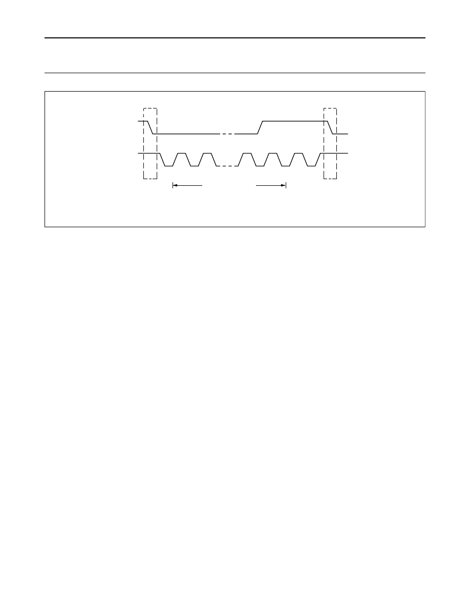
6.1
Data validity
The data on the SDA line must be stable during the HIGH
period of the clock. The HIGH or LOW state of the data line
can only change when the clock signal on the SCL line is
LOW (see Fig.4).
Fig.3 Connection of Standard- and Fast-mode devices to the I
2
C-bus.
MBC631
SCLKN1
OUT
SCLK
IN
SCLK
DATAN1
OUT
DATA
IN
DEVICE 1
SDA (Serial Data Line)
SCL (Serial Clock Line)
SCLKN2
OUT
SCLK
IN
SCLK
DATAN2
OUT
DATA
IN
DEVICE 2
VDD
R p
R p
pull-up
resistors
9
Philips Semiconductors
The I
2
C-bus specification
Fig.4 Bit transfer on the I
2
C-bus.
handbook, full pagewidth
MBC621
data line
stable;
data valid
change
of data
allowed
SDA
SCL
6.2
START and STOP conditions
Within the procedure of the I
2
C-bus, unique situations
arise which are defined as START (S) and STOP (P)
conditions (see Fig.5).
A HIGH to LOW transition on the SDA line while SCL is
HIGH is one such unique case. This situation indicates a
START condition.
A LOW to HIGH transition on the SDA line while SCL is
HIGH defines a STOP condition.
START and STOP conditions are always generated by the
master. The bus is considered to be busy after the START
condition. The bus is considered to be free again a certain
time after the STOP condition. This bus free situation is
specified in Section 15.
The bus stays busy if a repeated START (Sr) is generated
instead of a STOP condition. In this respect, the START
(S) and repeated START (Sr) conditions are functionally
identical (see Fig. 10). For the remainder of this document,
therefore, the S symbol will be used as a generic term to
represent both the START and repeated START
conditions, unless Sr is particularly relevant.
Detection of START and STOP conditions by devices
connected to the bus is easy if they incorporate the
necessary interfacing hardware. However,
microcontrollers with no such interface have to sample the
SDA line at least twice per clock period to sense the
transition.
Fig.5 START and STOP conditions.
handbook, full pagewidth
MBC622
SDA
SCL
P
STOP condition
SDA
SCL
S
START condition
10
Philips Semiconductors
The I
2
C-bus specification
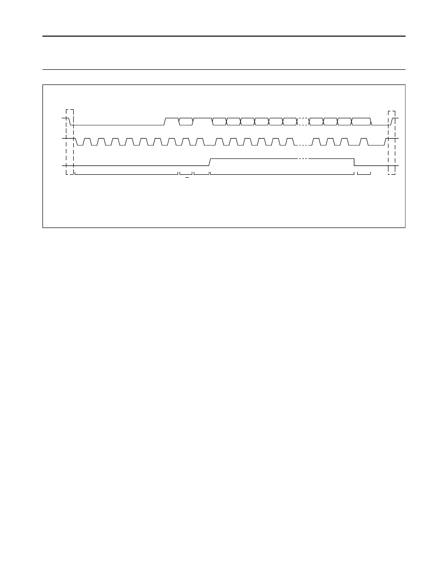
7
TRANSFERRING DATA
7.1
Byte format
Every byte put on the SDA line must be 8-bits long. The
number of bytes that can be transmitted per transfer is
unrestricted. Each byte has to be followed by an
acknowledge bit. Data is transferred with the most
significant bit (MSB) first (see Fig.6). If a slave can’t
receive or transmit another complete byte of data until it
has performed some other function, for example servicing
an internal interrupt, it can hold the clock line SCL LOW to
force the master into a wait state. Data transfer then
continues when the slave is ready for another byte of data
and releases clock line SCL.
In some cases, it’s permitted to use a different format from
the I
2
C-bus format (for CBUS compatible devices for
example). A message which starts with such an address
can be terminated by generation of a STOP condition,
even during the transmission of a byte. In this case, no
acknowledge is generated (see Section 10.1.3).
7.2
Acknowledge
Data transfer with acknowledge is obligatory. The
acknowledge-related clock pulse is generated by the
master. The transmitter releases the SDA line (HIGH)
during the acknowledge clock pulse.
The receiver must pull down the SDA line during the
acknowledge clock pulse so that it remains stable LOW
during the HIGH period of this clock pulse (see Fig.7). Of
course, set-up and hold times (specified in Section 15)
must also be taken into account.
Usually, a receiver which has been addressed is obliged to
generate an acknowledge after each byte has been
received, except when the message starts with a CBUS
address (see Section 10.1.3).
When a slave doesn’t acknowledge the slave address (for
example, it’s unable to receive or transmit because it’s
performing some real-time function), the data line must be
left HIGH by the slave. The master can then generate
either a STOP condition to abort the transfer, or a repeated
START condition to start a new transfer.
If a slave-receiver does acknowledge the slave address
but, some time later in the transfer cannot receive any
more data bytes, the master must again abort the transfer.
This is indicated by the slave generating the
not-acknowledge on the first byte to follow. The slave
leaves the data line HIGH and the master generates a
STOP or a repeated START condition.
If a master-receiver is involved in a transfer, it must signal
the end of data to the slave- transmitter by not generating
an acknowledge on the last byte that was clocked out of
the slave. The slave-transmitter must release the data line
to allow the master to generate a STOP or repeated
START condition.
Fig.6 Data transfer on the I
2
C-bus.
handbook, full pagewidth
MSC608
Sr
or
P
SDA
Sr
P
SCL
STOP or
repeated START
condition
S
or
Sr
START or
repeated START
condition
1
2
3 - 8
9
ACK
9
ACK
7
8
1
2
MSB
acknowledgement
signal from slave
byte complete,
interrupt within slave
clock line held low while
interrupts are serviced
acknowledgement
signal from receiver
11
Philips Semiconductors
The I
2
C-bus specification
Fig.7 Acknowledge on the I
2
C-bus.
handbook, full pagewidth
MBC602
S
START
condition
9
8
2
1
clock pulse for
acknowledgement
not acknowledge
acknowledge
DATA OUTPUT
BY TRANSMITTER
DATA OUTPUT
BY RECEIVER
SCL FROM
MASTER
8
ARBITRATION AND CLOCK GENERATION
8.1
Synchronization
All masters generate their own clock on the SCL line to
transfer messages on the I
2
C-bus. Data is only valid during
the HIGH period of the clock. A defined clock is therefore
needed for the bit-by-bit arbitration procedure to take
place.
Clock synchronization is performed using the wired-AND
connection of I
2
C interfaces to the SCL line. This means
that a HIGH to LOW transition on the SCL line will cause
the devices concerned to start counting off their LOW
period and, once a device clock has gone LOW, it will hold
the SCL line in that state until the clock HIGH state is
reached (see Fig.8). However, the LOW to HIGH transition
of this clock may not change the state of the SCL line if
another clock is still within its LOW period. The SCL line
will therefore be held LOW by the device with the longest
LOW period. Devices with shorter LOW periods enter a
HIGH wait-state during this time.
Fig.8 Clock synchronization during the arbitration procedure.
CLK
1
CLK
2
SCL
counter
reset
wait
state
start counting
HIGH period
MBC632
12
Philips Semiconductors
The I
2
C-bus specification
When all devices concerned have counted off their LOW
period, the clock line will be released and go HIGH. There
will then be no difference between the device clocks and
the state of the SCL line, and all the devices will start
counting their HIGH periods. The first device to complete
its HIGH period will again pull the SCL line LOW.
In this way, a synchronized SCL clock is generated with its
LOW period determined by the device with the longest
clock LOW period, and its HIGH period determined by the
one with the shortest clock HIGH period.
8.2
Arbitration
A master may start a transfer only if the bus is free. Two or
more masters may generate a START condition within the
minimum hold time (t
HD;STA
) of the START condition which
results in a defined START condition to the bus.
Arbitration takes place on the SDA line, while the SCL line
is at the HIGH level, in such a way that the master which
transmits a HIGH level, while another master is
transmitting a LOW level will switch off its DATA output
stage because the level on the bus doesn’t correspond to
its own level.
Arbitration can continue for many bits. Its first stage is
comparison of the address bits (addressing information is
given in Sections 10 and 14). If the masters are each trying
to address the same device, arbitration continues with
comparison of the data-bits if they are master-transmitter,
or acknowledge-bits if they are master-receiver. Because
address and data information on the I
2
C-bus is determined
by the winning master, no information is lost during the
arbitration process.
A master that loses the arbitration can generate clock
pulses until the end of the byte in which it loses the
arbitration.
As an Hs-mode master has a unique 8-bit master code, it
will always finish the arbitration during the first byte (see
Section 13).
If a master also incorporates a slave function and it loses
arbitration during the addressing stage, it’s possible that
the winning master is trying to address it. The losing
master must therefore switch over immediately to its slave
mode.
Figure 9 shows the arbitration procedure for two masters.
Of course, more may be involved (depending on how
many masters are connected to the bus). The moment
there is a difference between the internal data level of the
master generating DATA 1 and the actual level on the SDA
line, its data output is switched off, which means that a
HIGH output level is then connected to the bus. This will
not affect the data transfer initiated by the winning master.
Fig.9 Arbitration procedure of two masters.
handbook, full pagewidth
MSC609
DATA
1
DATA
2
SDA
SCL
S
master 1 loses arbitration
DATA 1 SDA
13
Philips Semiconductors
The I
2
C-bus specification
Since control of the I
2
C-bus is decided solely on the
address or master code and data sent by competing
masters, there is no central master, nor any order of
priority on the bus.
Special attention must be paid if, during a serial transfer,
the arbitration procedure is still in progress at the moment
when a repeated START condition or a STOP condition is
transmitted to the I
2
C-bus. If it’s possible for such a
situation to occur, the masters involved must send this
repeated START condition or STOP condition at the same
position in the format frame. In other words, arbitration isn’t
allowed between:
•
A repeated START condition and a data bit
•
A STOP condition and a data bit
•
A repeated START condition and a STOP condition.
Slaves are not involved in the arbitration procedure.
8.3
Use of the clock synchronizing mechanism as
a handshake
In addition to being used during the arbitration procedure,
the clock synchronization mechanism can be used to
enable receivers to cope with fast data transfers, on either
a byte level or a bit level.
On the byte level, a device may be able to receive bytes of
data at a fast rate, but needs more time to store a received
byte or prepare another byte to be transmitted. Slaves can
then hold the SCL line LOW after reception and
acknowledgment of a byte to force the master into a wait
state until the slave is ready for the next byte transfer in a
type of handshake procedure (see Fig.6).
On the bit level, a device such as a microcontroller with or
without limited hardware for the I
2
C-bus, can slow down
the bus clock by extending each clock LOW period. The
speed of any master is thereby adapted to the internal
operating rate of this device.
In Hs-mode, this handshake feature can only be used on
byte level (see Section 13).
9
FORMATS WITH 7-BIT ADDRESSES
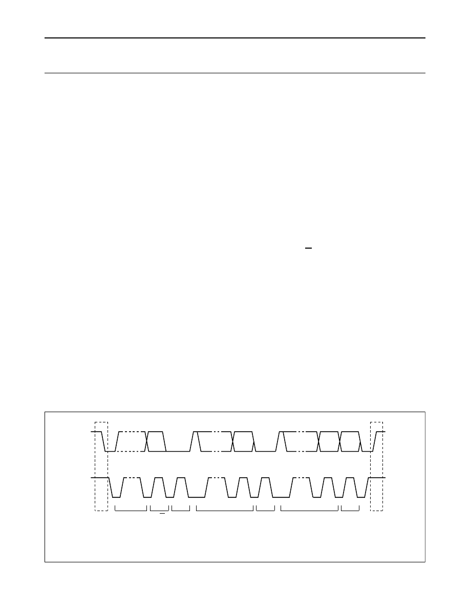
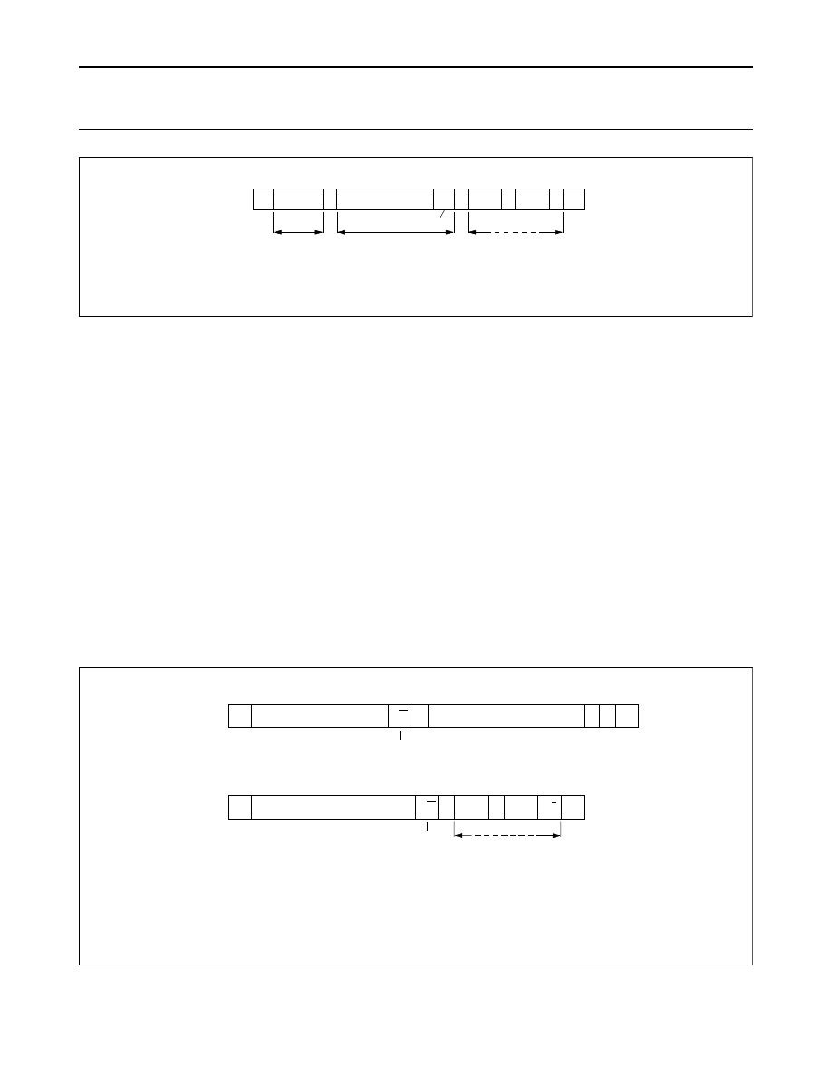
Data transfers follow the format shown in Fig.10. After the
START condition (S), a slave address is sent. This
address is 7 bits long followed by an eighth bit which is a
data direction bit (R/W) - a ‘zero’ indicates a transmission
(WRITE), a ‘one’ indicates a request for data (READ). A
data transfer is always terminated by a STOP condition (P)
generated by the master. However, if a master still wishes
to communicate on the bus, it can generate a repeated
START condition (Sr) and address another slave without
first generating a STOP condition. Various combinations of
read/write formats are then possible within such a transfer.
Fig.10 A complete data transfer.
handbook, full pagewidth
S
1 – 7
8
9
1 – 7
8
9
1 – 7
8
9
P
STOP
condition
START
condition
DATA
ACK
DATA
ACK
ADDRESS
ACK
R/W
SDA
SCL
MBC604
14
Philips Semiconductors
The I
2
C-bus specification
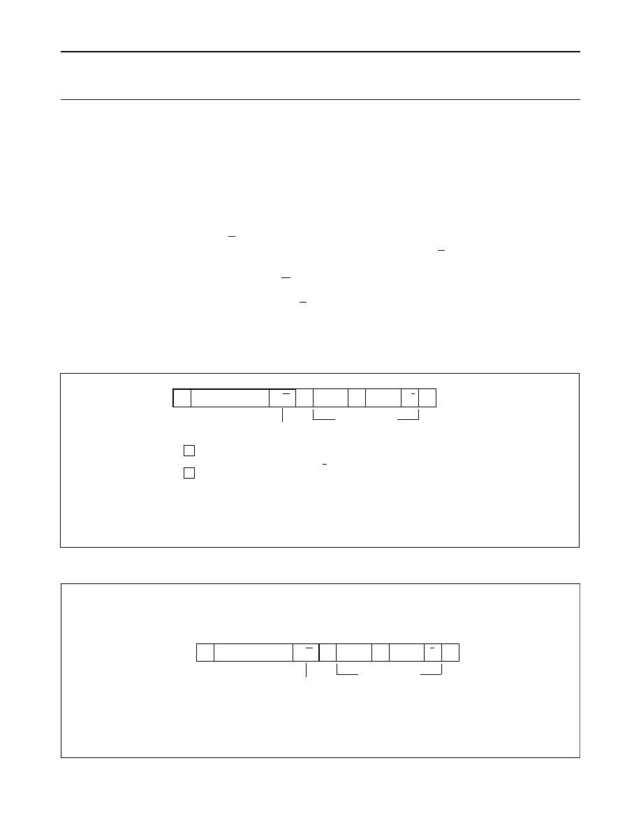
Possible data transfer formats are:
•
Master-transmitter transmits to slave-receiver. The
transfer direction is not changed (see Fig.11).
•
Master reads slave immediately after first byte (see
Fig.12). At the moment of the first acknowledge, the
master- transmitter becomes a master- receiver and the
slave-receiver becomes a slave-transmitter. This first
acknowledge is still generated by the slave. The STOP
condition is generated by the master, which has
previously sent a not-acknowledge (A).
•
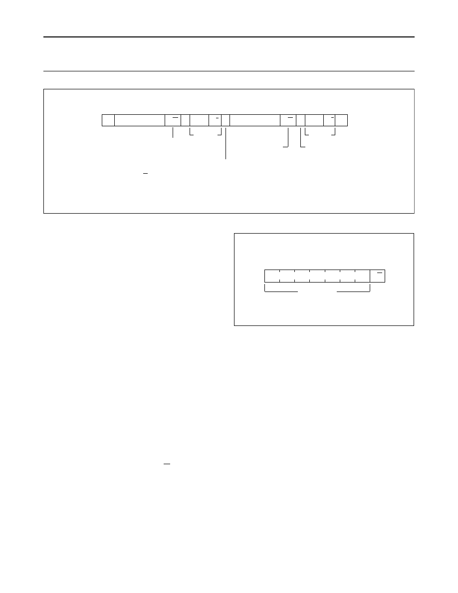
Combined format (see Fig.13). During a change of
direction within a transfer, the START condition and the
slave address are both repeated, but with the R/W bit
reversed. If a master receiver sends a repeated START
condition, it has previously sent a not-acknowledge (A).
NOTES:
1.
Combined formats can be used, for example, to
control a serial memory. During the first data byte, the
internal memory location has to be written. After the
START condition and slave address is repeated, data
can be transferred.
2.
All decisions on auto-increment or decrement of
previously accessed memory locations etc. are taken
by the designer of the device.
3.
Each byte is followed by an acknowledgment bit as
indicated by the A or A blocks in the sequence.
4.
I
2
C-bus compatible devices must reset their bus logic
on receipt of a START or repeated START condition
such that they all anticipate the sending of a slave
address, even if these START conditions are not
positioned according to the proper format.
5.
A START condition immediately followed by a STOP
condition (void message) is an illegal format.
Fig.11 A master-transmitter addressing a slave receiver with a 7-bit address.
The transfer direction is not changed.
handbook, full pagewidth
,,
,,
,,,
,,,
,,,
,,,
,,,,,,
,,,,,,
MBC605
A/A
A
'0' (write)
data transferred
(n bytes + acknowledge)
A = acknowledge (SDA LOW)
A = not acknowledge (SDA HIGH)
S = START condition
P = STOP condition
R/W
from master to slave
from slave to master
,,
DATA
DATA
A
SLAVE ADDRESS
S
P
Fig.12 A master reads a slave immediately after the first byte.
handbook, full pagewidth
,,
,,
,,
,,
,,,,,,
,,,,,,
MBC606
A
(read)
data transferred
(n bytes + acknowledge)
R/W
A
1
P
DATA
DATA
SLAVE ADDRESS
S
A
15
Philips Semiconductors
The I
2
C-bus specification
Fig.13 Combined format.
handbook, full pagewidth
,
,,,,,
,,,,,
MBC607
DATA
A
R/W
read or write
A/A
DATA
A
R/W
(n bytes
+ ack.)
direction
of transfer
may change
at this point.
read or write
(n bytes
+ ack.)
Sr = repeated START condition
A/A
*
*
*
not shaded because
transfer direction of
data and acknowledge bits
depends on R/W bits.
SLAVE ADDRESS
S
Sr
P
SLAVE ADDRESS
10 7-BIT ADDRESSING
The addressing procedure for the I
2
C-bus is such that the
first byte after the START condition usually determines
which slave will be selected by the master. The exception
is the ‘general call’ address which can address all devices.
When this address is used, all devices should, in theory,
respond with an acknowledge. However, devices can be
made to ignore this address. The second byte of the
general call address then defines the action to be taken.
This procedure is explained in more detail in
Section 10.1.1. For information on 10-bit addressing, see
Section 14
10.1
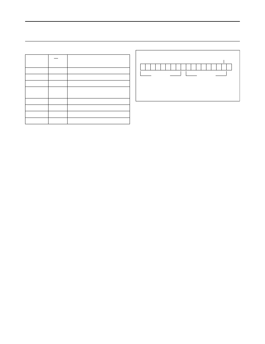
Definition of bits in the first byte
The first seven bits of the first byte make up the slave
address (see Fig.14). The eighth bit is the LSB (least
significant bit). It determines the direction of the message.
A ‘zero’ in the least significant position of the first byte
means that the master will write information to a selected
slave. A ‘one’ in this position means that the master will
read information from the slave.
When an address is sent, each device in a system
compares the first seven bits after the START condition
with its address. If they match, the device considers itself
addressed by the master as a slave-receiver or
slave-transmitter, depending on the R/W bit.
A slave address can be made-up of a fixed and a
programmable part. Since it’s likely that there will be
several identical devices in a system, the programmable
part of the slave address enables the maximum possible
number of such devices to be connected to the I
2
C-bus.
The number of programmable address bits of a device
depends on the number of pins available. For example, if
a device has 4 fixed and 3 programmable address bits, a
total of 8 identical devices can be connected to the same
bus.
The I
2
C-bus committee coordinates allocation of I
2
C
addresses. Further information can be obtained from the
Philips representatives listed on the back cover. Two
groups of eight addresses (0000XXX and 1111XXX) are
reserved for the purposes shown in Table 2. The bit
combination 11110XX of the slave address is reserved for
10-bit addressing (see Section 14).
Fig.14 The first byte after the START procedure.
handbook, halfpage
MBC608
R/W
LSB
MSB
slave address
16
Philips Semiconductors
The I
2
C-bus specification
Table 2
Definition of bits in the first byte
Notes
1.
No device is allowed to acknowledge at the reception
of the START byte.
2.
The CBUS address has been reserved to enable the
inter-mixing of CBUS compatible and I
2
C-bus
compatible devices in the same system. I
2
C-bus
compatible devices are not allowed to respond on
reception of this address.
3.
The address reserved for a different bus format is
included to enable I
2
C and other protocols to be mixed.
Only I
2
C-bus compatible devices that can work with
such formats and protocols are allowed to respond to
this address.
10.1.1
G
ENERAL
CALL
ADDRESS
The general call address is for addressing every device
connected to the I
2
C-bus. However, if a device doesn’t
need any of the data supplied within the general call
structure, it can ignore this address by not issuing an
acknowledgment. If a device does require data from a
general call address, it will acknowledge this address and
behave as a slave- receiver. The second and following
bytes will be acknowledged by every slave- receiver
capable of handling this data. A slave which cannot
process one of these bytes must ignore it by
not-acknowledging. The meaning of the general call
address is always specified in the second byte (see
Fig.15).
There are two cases to consider:
•
When the least significant bit B is a ‘zero’.
•
When the least significant bit B is a ‘one’.
When bit B is a ‘zero’; the second byte has the following
definition:
•
00000110 (H‘06’). Reset and write programmable part
of slave address by hardware. On receiving this 2-byte
sequence, all devices designed to respond to the
general call address will reset and take in the
programmable part of their address. Pre-cautions have
to be taken to ensure that a device is not pulling down
the SDA or SCL line after applying the supply voltage,
since these low levels would block the bus.
•
00000100 (H‘04’). Write programmable part of slave
address by hardware. All devices which define the
programmable part of their address by hardware (and
which respond to the general call address) will latch this
programmable part at the reception of this two byte
sequence. The device will not reset.
•
00000000 (H‘00’). This code is not allowed to be used as
the second byte.
Sequences of programming procedure are published in
the appropriate device data sheets.
The remaining codes have not been fixed and devices
must ignore them.
When bit B is a ‘one’; the 2-byte sequence is a ‘hardware
general call’. This means that the sequence is transmitted
by a hardware master device, such as a keyboard
scanner, which cannot be programmed to transmit a
desired slave address. Since a hardware master doesn’t
know in advance to which device the message has to be
transferred, it can only generate this hardware general call
and its own address - identifying itself to the system (see
Fig.16).
The seven bits remaining in the second byte contain the
address of the hardware master. This address is
recognized by an intelligent device (e.g. a microcontroller)
connected to the bus which will then direct the information
from the hardware master. If the hardware master can also
act as a slave, the slave address is identical to the master
address.
SLAVE
ADDRESS
R/W BIT
DESCRIPTION
0000 000
0
General call address
0000 000
1
START byte
(1)
0000 001
X
CBUS address
(2)
0000 010
X
Reserved for different bus
format
(3)
0000 011
X
Reserved for future purposes
0000 1XX
X
Hs-mode master code
1111 1XX
X
Reserved for future purposes
1111 0XX
X
10-bit slave addressing
Fig.15 General call address format.
MBC623
LSB
second byte
0
0
0
0
0
0
0
0
A
X
X
X X
X
X
X
B
A
first byte
(general call address)
17
Philips Semiconductors
The I
2
C-bus specification
Fig.16 Data transfer from a hardware master-transmitter.
handbook, full pagewidth
,,,
,,,,,
,,
,,,
MBC624
general
call address
(B)
A
A
second
byte
A
A
(n bytes + ack.)
S
00000000
MASTER ADDRESS
1
P
DATA
DATA
In some systems, an alternative could be that the
hardware master transmitter is set in the slave-receiver
mode after the system reset. In this way, a system
configuring master can tell the hardware master-
transmitter (which is now in slave-receiver mode) to which
address data must be sent (see Fig.17). After this
programming procedure, the hardware master remains in
the master-transmitter mode.
10.1.2
START
BYTE
Microcontrollers can be connected to the I
2
C-bus in two
ways. A microcontroller with an on-chip hardware I
2
C-bus
interface can be programmed to be only interrupted by
requests from the bus. When the device doesn’t have such
an interface, it must constantly monitor the bus via
software. Obviously, the more times the microcontroller
monitors, or polls the bus, the less time it can spend
carrying out its intended function.
There is therefore a speed difference between fast
hardware devices and a relatively slow microcontroller
which relies on software polling.
In this case, data transfer can be preceded by a start
procedure which is much longer than normal (see Fig.18).
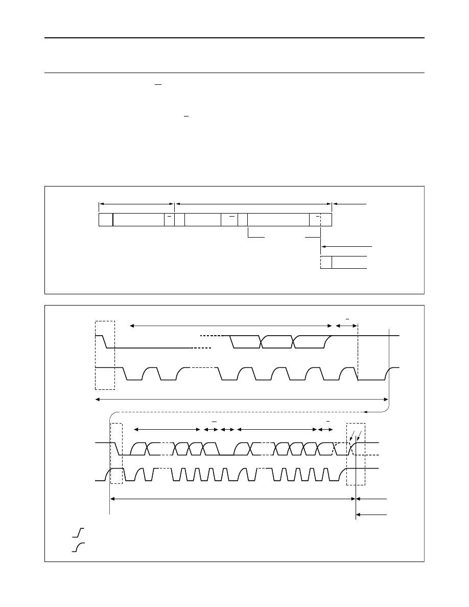
The start procedure consists of:
•
A START condition (S)
•
A START byte (00000001)
•
An acknowledge clock pulse (ACK)
•
A repeated START condition (Sr).
Fig.17 Data transfer by a hardware-transmitter capable of dumping data directly to slave devices.
(a) Configuring master sends dump address to hardware master
(b) Hardware master dumps data to selected slave.
handbook, full pagewidth
,,,,,,,
,,,,,,,
,,
,,
,,
,,
,,
,,
,,
,,
,,,,,,
,,,,,,
,,,,,,
,,,,,,
MBC609
write
A
A
(a)
(b)
R/W
write
A
A
(n bytes + ack.)
A/A
R/W
S
P
SLAVE ADDR. H/W MASTER
DUMP ADDR. FOR H/W MASTER X
S
P
DUMP ADDR. FROM H/W MASTER
DATA
DATA
18
Philips Semiconductors
The I
2
C-bus specification
Fig.18 START byte procedure.
MBC633
S
9
8
2
1
Sr
7
ACK
dummy
acknowledge
(HIGH)
start byte 00000001
SDA
SCL
After the START condition S has been transmitted by a
master which requires bus access, the START byte
(00000001) is transmitted. Another microcontroller can
therefore sample the SDA line at a low sampling rate until
one of the seven zeros in the START byte is detected.
After detection of this LOW level on the SDA line, the
microcontroller can switch to a higher sampling rate to find
the repeated START condition Sr which is then used for
synchronization.
A hardware receiver will reset on receipt of the repeated
START condition Sr and will therefore ignore the START
byte.
An acknowledge-related clock pulse is generated after the
START byte. This is present only to conform with the byte
handling format used on the bus. No device is allowed to
acknowledge the START byte.
10.1.3
CBUS
COMPATIBILITY
CBUS receivers can be connected to the Standard-mode
I
2
C-bus. However, a third bus line called DLEN must then
be connected and the acknowledge bit omitted. Normally,
I
2
C transmissions are sequences of 8-bit bytes; CBUS
compatible devices have different formats.
In a mixed bus structure, I
2
C-bus devices must not
respond to the CBUS message. For this reason, a special
CBUS address (0000001X) to which no I
2
C-bus
compatible device will respond, has been reserved. After
transmission of the CBUS address, the DLEN line can be
made active and a CBUS-format transmission sent (see
Fig.19). After the STOP condition, all devices are again
ready to accept data.
Master-transmitters can send CBUS formats after sending
the CBUS address. The transmission is ended by a STOP
condition, recognized by all devices.
NOTE: If the CBUS configuration is known, and expansion
with CBUS compatible devices isn’t foreseen, the designer
is allowed to adapt the hold time to the specific
requirements of the device(s) used.
19
Philips Semiconductors
The I
2
C-bus specification
MBC634
S
P
STOP
condition
CBUS
load pulse
n - data bits
CBUS
address
START
condition
R/W
bit
ACK
related
clock pulse
SDA
SCL
DLEN
Fig.19 Data format of transmissions with CBUS transmitter/receiver.
11 EXTENSIONS TO THE STANDARD-MODE I
2
C-BUS
SPECIFICATION
The Standard-mode I
2
C-bus specification, with its data
transfer rate of up to 100 kbit/s and 7-bit addressing, has
been in existence since the beginning of the 1980’s. This
concept rapidly grew in popularity and is today accepted
worldwide as a de facto standard with several hundred
different compatible ICs on offer from Philips
Semiconductors and other suppliers. To meet the
demands for higher speeds, as well as make available
more slave address for the growing number of new
devices, the Standard-mode I
2
C-bus specification was
upgraded over the years and today is available with the
following extensions:
•
Fast-mode, with a bit rate up to 400 kbit/s.
•
High-speed mode (Hs-mode), with a bit rate up to
3.4 Mbit/s.
•
10-bit addressing, which allows the use of up to 1024
additional slave addresses.
There are two main reasons for extending the regular
I
2
C-bus specification:
•
Many of today’s applications need to transfer large
amounts of serial data and require bit rates far in excess
of 100 kbit/s (Standard-mode), or even 400 kbit/s
(Fast-mode). As a result of continuing improvements in
semiconductor technologies, I
2
C-bus devices are now
available with bit rates of up to 3.4 Mbit/s (Hs-mode)
without any noticeable increases in the manufacturing
cost of the interface circuitry.
•
As most of the 112 addresses available with the 7-bit
addressing scheme were soon allocated, it became
apparent that more address combinations were required
to prevent problems with the allocation of slave
addresses for new devices. This problem was resolved
with the new 10-bit addressing scheme, which allowed
about a tenfold increase in available addresses.
New slave devices with a Fast- or Hs-mode I
2
C-bus
interface can have a 7- or a 10-bit slave address. If
possible, a 7-bit address is preferred as it is the cheapest
hardware solution and results in the shortest message
length. Devices with 7- and 10-bit addresses can be mixed
in the same I
2
C-bus system regardless of whether it is an
F/S- or Hs-mode system. Both existing and future masters
can generate either 7- or 10-bit addresses.
12 FAST-MODE
With the Fast-mode I
2
C-bus specification, the protocol,
format, logic levels and maximum capacitive load for the
SDA and SCL lines quoted in the Standard-mode I
2
C-bus
specification are unchanged. New devices with an I
2
C-bus
interface must meet at least the minimum requirements of
the Fast- or Hs-mode specification (see Section 13).
Fast-mode devices can receive and transmit at up to
400 kbit/s. The minimum requirement is that they can
synchronize with a 400 kbit/s transfer; they can then
prolong the LOW period of the SCL signal to slow down the
transfer. Fast-mode devices are downward-compatible
and can communicate with Standard-mode devices in a
0 to 100 kbit/s I
2
C-bus system. As Standard-mode
devices, however, are not upward compatible, they should
not be incorporated in a Fast-mode I
2
C-bus system as
they cannot follow the higher transfer rate and
unpredictable states would occur.

20
Philips Semiconductors
The I
2
C-bus specification
The Fast-mode I
2
C-bus specification has the following
additional features compared with the Standard-mode:
•
The maximum bit rate is increased to 400 kbit/s.
•
Timing of the serial data (SDA) and serial clock (SCL)
signals has been adapted. There is no need for
compatibility with other bus systems such as CBUS
because they cannot operate at the increased bit rate.
•
The inputs of Fast-mode devices incorporate spike
suppression and a Schmitt trigger at the SDA and SCL
inputs.
•
The output buffers of Fast-mode devices incorporate
slope control of the falling edges of the SDA and SCL
signals.
•
If the power supply to a Fast-mode device is switched
off, the SDA and SCL I/O pins must be floating so that
they don’t obstruct the bus lines.
•
The external pull-up devices connected to the bus lines
must be adapted to accommodate the shorter maximum
permissible rise time for the Fast-mode I
2
C-bus. For bus
loads up to 200 pF, the pull-up device for each bus line
can be a resistor; for bus loads between 200 pF and
400 pF, the pull-up device can be a current source
(3 mA max.) or a switched resistor circuit (see Fig.43).
13 Hs-MODE
High-speed mode (Hs-mode) devices offer a quantum
leap in I
2
C-bus transfer speeds. Hs-mode devices can
transfer information at bit rates of up to 3.4 Mbit/s, yet they
remain fully downward compatible with Fast- or
Standard-mode (F/S-mode) devices for bi-directional
communication in a mixed-speed bus system. With the
exception that arbitration and clock synchronization is not
performed during the Hs-mode transfer, the same serial
bus protocol and data format is maintained as with the
F/S-mode system. Depending on the application, new
devices may have a Fast or Hs-mode I
2
C-bus interface,
although Hs-mode devices are preferred as they can be
designed-in to a greater number of applications.
13.1
High speed transfer
To achieve a bit transfer of up to 3.4 Mbit/s the following
improvements have been made to the regular I
2
C-bus
specification:
•
Hs-mode master devices have an open-drain output
buffer for the SDAH signal and a combination of an
open-drain pull-down and current-source pull-up circuit
on the SCLH output
(1)
. This current-source circuit
shortens the rise time of the SCLH signal. Only the
current-source of one master is enabled at any one time,
and only during Hs-mode.
•
No arbitration or clock synchronization is performed
during Hs-mode transfer in multi-master systems, which
speeds-up bit handling capabilities. The arbitration
procedure always finishes after a preceding master
code transmission in F/S-mode.
•
Hs-mode master devices generate a serial clock signal
with a HIGH to LOW ratio of 1 to 2. This relieves the
timing requirements for set-up and hold times.
•
As an option, Hs-mode master devices can have a
built-in bridge
(1)
. During Hs-mode transfer, the high
speed data (SDAH) and high-speed serial clock (SCLH)
lines of Hs-mode devices are separated by this bridge
from the SDA and SCL lines of F/S-mode devices. This
reduces the capacitive load of the SDAH and SCLH
lines resulting in faster rise and fall times.
•
The only difference between Hs-mode slave devices
and F/S-mode slave devices is the speed at which they
operate. Hs-mode slaves have open-drain output buffers
on the SCLH and SDAH outputs. Optional pull-down
transistors on the SCLH pin can be used to stretch the
LOW level of the SCLH signal, although this is only
allowed after the acknowledge bit in Hs-mode transfers.
•
The inputs of Hs-mode devices incorporate spike
suppression and a Schmitt trigger at the SDAH and
SCLH inputs.
•
The output buffers of Hs-mode devices incorporate
slope control of the falling edges of the SDAH and SCLH
signals.
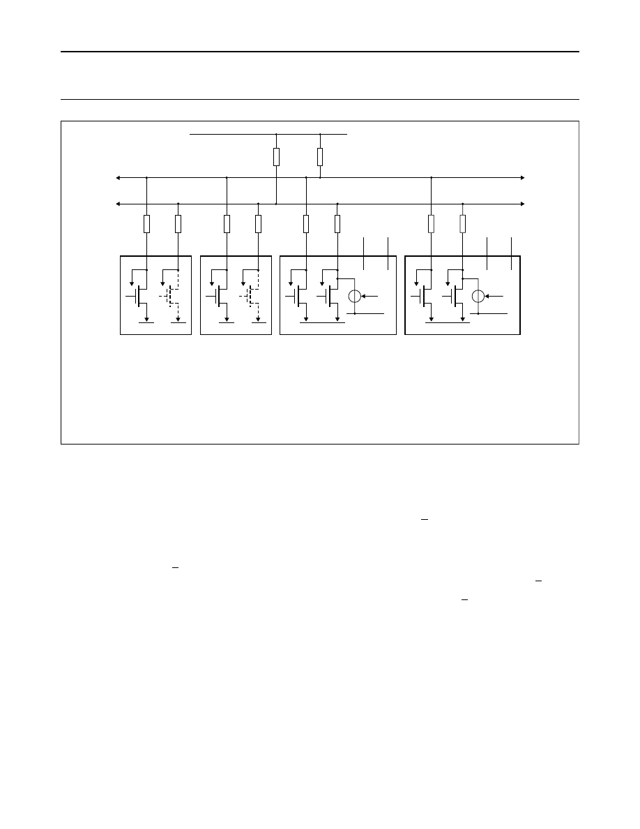
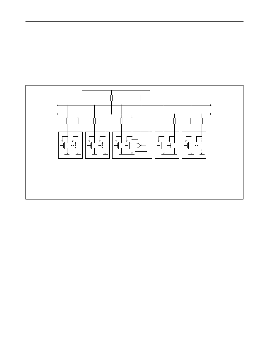
Figure 20 shows the physical I
2
C-bus configuration in a
system with only Hs-mode devices. Pins SDA and SCL on
the master devices are only used in mixed-speed bus
systems and are not connected in an Hs-mode only
system. In such cases, these pins can be used for other
functions.
Optional series resistors R
s
protect the I/O stages of the
I
2
C-bus devices from high-voltage spikes on the bus lines
and minimize ringing and interference.
Pull-up resistors R
p
maintain the SDAH and SCLH lines at
a HIGH level when the bus is free and ensure the signals
are pulled up from a LOW to a HIGH level within the
required rise time. For higher capacitive bus-line loads
(>100 pF), the resistor R
p
can be replaced by external
current source pull-ups to meet the rise time requirements.
Unless proceeded by an acknowledge bit, the rise time of
the SCLH clock pulses in Hs-mode transfers is shortened
by the internal current-source pull-up circuit MCS of the
active master.
(1) Patent application pending.
21
Philips Semiconductors
The I
2
C-bus specification
Fig.20 I
2
C-bus configuration with Hs-mode devices only.
handbook, full pagewidth
MSC612
VSS
SLAVE
SDAH
SCLH
VSS
MASTER/SLAVE
SDAH
SCLH
SDA
MCS
SCL
Rs
Rs
SLAVE
SDAH
SCLH
VSS
Rs
Rs
Rs
Rs
VDD
VSS
MASTER/SLAVE
SDAH
SCLH
SDA
SCL
Rs
Rs
VDD
(1)
(1)
(1)
(1)
(2)
(2)
(4)
(4)
(3)
MCS
(3)
(2)
(2)
(2)
(2)
(2)
(2)
VDD
Rp
Rp
SCLH
SDAH
(1) SDA and SCL are not used here but may be used for other functions.
(2) To input filter.
(3) Only the active master can enable its current-source pull-up circuit
(4) Dotted transistors are optional open-drain outputs which can stretch the serial clock signal SCLH.
13.2
Serial data transfer format in Hs-mode
Serial data transfer format in Hs-mode meets the
Standard-mode I
2
C-bus specification. Hs-mode can only
commence after the following conditions (all of which are
in F/S-mode):
1.
START condition (S)
2.
8-bit master code (00001XXX)
3.
not-acknowledge bit (A)
Figures 21 and 22 show this in more detail. This master
code has two main functions:
•
It allows arbitration and synchronization between
competing masters at F/S-mode speeds, resulting in
one winning master.
•
It indicates the beginning of an Hs-mode transfer.
Hs-mode master codes are reserved 8-bit codes, which
are not used for slave addressing or other purposes.
Furthermore, as each master has its own unique master
code, up to eight Hs-mode masters can be present on the
one I
2
C-bus system (although master code 0000 1000
should be reserved for test and diagnostic purposes). The
master code for an Hs-mode master device is software
programmable and is chosen by the System Designer.
Arbitration and clock synchronization only take place
during the transmission of the master code and
not-acknowledge bit (A), after which one winning master
remains active. The master code indicates to other devices
that an Hs-mode transfer is to begin and the connected
devices must meet the Hs-mode specification. As no
device is allowed to acknowledge the master code, the
master code is followed by a not-acknowledge (A).
After the not-acknowledge bit (A), and the SCLH line has
been pulled-up to a HIGH level, the active master switches
to Hs-mode and enables (at time t
H
, see Fig.22) the
current-source pull-up circuit for the SCLH signal. As other
devices can delay the serial transfer before t
H
by stretching
the LOW period of the SCLH signal, the active master will
enable its current-source pull-up circuit when all devices
have released the SCLH line and the SCLH signal has
reached a HIGH level, thus speeding up the last part of the
rise time of the SCLH signal.
The active master then sends a repeated START condition
(Sr) followed by a 7-bit slave address (or 10-bit slave
22
Philips Semiconductors
The I
2
C-bus specification
address, see Section 14) with a R/W bit address, and
receives an acknowledge bit (A) from the selected slave.
After a repeated START condition and after each
acknowledge bit (A) or not-acknowledge bit (A), the active
master disables its current-source pull-up circuit. This
enables other devices to delay the serial transfer by
stretching the LOW period of the SCLH signal. The active
master re-enables its current-source pull-up circuit again
when all devices have released and the SCLH signal
reaches a HIGH level, and so speeds up the last part of
the SCLH signal’s rise time.
Data transfer continues in Hs-mode after the next
repeated START (Sr), and only switches back to
F/S-mode after a STOP condition (P). To reduce the
overhead of the master code, it’s possible that a master
links a number of Hs-mode transfers, separated by
repeated START conditions (Sr).
handbook, full pagewidth
,,
,,
,,,,,
,,,,,
,,,,,
,,,,,
F/S-mode
Hs-mode (current-source for SCLH enabled)
F/S-mode
MSC616
A
A
A/A
DATA
(n bytes
+
ack.)
S
R/W
MASTER CODE
Sr
SLAVE ADD.
Hs-mode continues
,,,,
,,,,
Sr SLAVE ADD.
P
Fig.21 Data transfer format in Hs-mode.
handbook, full pagewidth
MSC618
8-bit Master code 00001xxx
A
tH
t1
S
F/S mode
Hs-mode
If P then
F/S mode
If Sr (dotted lines)
then Hs-mode
1
6
7
8
9
6
7
8
9
1
1
2 to 5
2 to 5
2 to 5
6
7
8
9
SDAH
SCLH
SDAH
SCLH
tH
tFS
Sr
Sr P
n
×
(8-bit DATA
+
A/A)
7-bit SLA
R/W
A
= MCS current source pull-up
= Rp resistor pull-up
Fig.22 A complete Hs-mode transfer.

23
Philips Semiconductors
The I
2
C-bus specification
13.3
Switching from F/S- to Hs-mode and back
After reset and initialization, Hs-mode devices must be in
Fast-mode (which is in effect F/S-mode as Fast-mode is
downward compatible with Standard-mode). Each
Hs-mode device can switch from Fast- to Hs-mode and
back and is controlled by the serial transfer on the I
2
C-bus.
Before time t
1
in Fig.22, each connected device operates
in Fast-mode. Between times t
1
and t
H
(this time interval
can be stretched by any device) each connected device
must recognize the “S 00001XXX A” sequence and has to
switch its internal circuit from the Fast-mode setting to the
Hs-mode setting. Between times t
1
and t
H
the connected
master and slave devices perform this switching by the
following actions.
The active (winning) master:
1.
Adapts its SDAH and SCLH input filters according to
the spike suppression requirement in Hs-mode.
2.
Adapts the set-up and hold times according to the
Hs-mode requirements.
3.
Adapts the slope control of its SDAH and SCLH output
stages according to the Hs-mode requirement.
4.
Switches to the Hs-mode bit-rate, which is required
after time t
H
.
5.
Enables the current source pull-up circuit of its SCLH
output stage at time t
H
.
The non-active, or losing masters:
1.
Adapt their SDAH and SCLH input filters according to
the spike suppression requirement in Hs-mode.
2.
Wait for a STOP condition to detect when the bus is
free again.
All slaves:
1.
Adapt their SDAH and SCLH input filters according to
the spike suppression requirement in Hs-mode.
2.
Adapt the set-up and hold times according to the
Hs-mode requirements. This requirement may already
be fulfilled by the adaptation of the input filters.
3.
Adapt the slope control of their SDAH output stages, if
necessary. For slave devices, slope control is
applicable for the SDAH output stage only and,
depending on circuit tolerances, both the Fast- and
Hs-mode requirements may be fulfilled without
switching its internal circuit.
At time t
FS
in Fig.22, each connected device must
recognize the STOP condition (P) and switch its internal
circuit from the Hs-mode setting back to the Fast-mode
setting as present before time t
1
. This must be completed
within the minimum bus free time as specified in Table 5
according to the Fast-mode specification.
24
Philips Semiconductors
The I
2
C-bus specification
13.4
Hs-mode devices at lower speed modes
Hs-mode devices are fully downwards compatible, and
can be connected to an F/S-mode I
2
C-bus system (see
Fig.23). As no master code will be transmitted in such a
configuration, all Hs-mode master devices stay in
F/S-mode and communicate at F/S-mode speeds with
their current-source disabled. The SDAH and SCLH pins
are used to connect to the F/S-mode bus system, allowing
the SDA and SCL pins (if present) on the Hs-mode master
device to be used for other functions.
Fig.23 Hs-mode devices at F/S-mode speed.
handbook, full pagewidth
VSS
VSS
Hs-mode
SLAVE
SDAH
SCLH
VSS
Hs-mode
MASTER/SLAVE
SDAH
SCLH
SDA
SCL
Rs
Rs
Hs-mode
SLAVE
SDAH
SCLH
VSS
Rs
Rs
F/S-mode
MASTER/SLAVE
SDA
SCL
Rs
Rs
F/S-mode
SLAVE
SDA
SCL
VSS
Rs
Rs
Rs
Rs
VDD
(1)
(2)
(2)
(4)
(4)
(4)
(2)
(2)
(2)
(2)
(2)
(2)
(2)
(2)
(3)
(1)
VDD
Rp
Rp
SCL
SDA
MSC613
(1) Bridge not used. SDA and SCL may have an alternative function.
(2) To input filter.
(3) The current-source pull-up circuit stays disabled.
(4) Dotted transistors are optional open-drain outputs which can stretch the serial clock signal SCL.
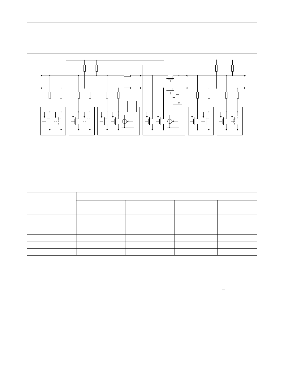
13.5
Mixed speed modes on one serial bus system
If a system has a combination of Hs-, Fast- and/or
Standard-mode devices, it’s possible, by using an
interconnection bridge, to have different bit rates between
different devices (see Figs 24 and 25).
One bridge is required to connect/disconnect an Hs-mode
section to/from an F/S-mode section at the appropriate
time. This bridge includes a level shift function that allows
devices with different supply voltages to be connected. For
example F/S-mode devices with a V
DD2
of 5 V can be
connected to Hs-mode devices with a V
DD1
of 3 V or less
(i.e. where V
DD2
≥
V
DD1
), provided SDA and SCL pins are
5 V tolerant. This bridge is incorporated in Hs-mode
master devices and is completely controlled by the serial
signals SDAH, SCLH, SDA and SCL. Such a bridge can be
implemented in any IC as an autonomous circuit.
TR1, TR2 and TR3 are N-channel transistors. TR1 and
TR2 have a transfer gate function, and TR3 is an open-
drain pull-down stage. If TR1 or TR2 are switched on they
transfer a LOW level in both directions, otherwise when
both the drain and source rise to a HIGH level there will be
a high impedance between the drain and source of each
switched on transistor. In the latter case, the transistors will
act as a level shifter as SDAH and SCLH will be pulled-up
to V
DD1
and SDA and SCL will be pulled-up to V
DD2
During F/S-mode speed, a bridge on one of the Hs-mode
masters connects the SDAH and SCLH lines to the
corresponding SDA and SCL lines thus permitting
Hs-mode devices to communicate with F/S-mode devices
at slower speeds. Arbitration and synchronization is
possible during the total F/S-mode transfer between all
connected devices as described in Section 8. During
Hs-mode transfer, however, the bridge opens to separate
the two bus sections and allows Hs-mode devices to
communicate with each other at 3.4 Mbit/s. Arbitration
between Hs-mode devices and F/S-mode devices is only
performed during the master code (00001XXX), and
normally won by one Hs-mode master as no slave address
has four leading zeros. Other masters can win the
arbitration only if they send a reserved 8-bit code
(00000XXX). In such cases, the bridge remains closed and
the transfer proceeds in F/S-mode. Table 3 gives the
possible communication speeds in such a system.
25
Philips Semiconductors
The I
2
C-bus specification
Table 3
Communication bit-rates in a mixed speed bus system
TRANSFER
BETWEEN
SERIAL BUS SYSTEM CONFIGURATION
Hs + FAST +
STANDARD
Hs + FAST
Hs + STANDARD
FAST +
STANDARD
Hs <–> Hs
0 to 3.4 Mbit/s
0 to 3.4 Mbit/s
0 to 3.4 Mbit/s
–
Hs <–> Fast
0 to 100 kbit/s
0 to 400 kbit/s
–
–
Hs <–> Standard
0 to 100 kbit/s
–
0 to 100 kbit/s
–
Fast <–> Standard
0 to 100 kbit/s
–
–
0 to 100 kbit/s
Fast <–> Fast
0 to 100 kbit/s
0 to 400 kbit/s
–
0 to 100 kbit/s
Standard <–> Standard
0 to 100 kbit/s
–
0 to 100 kbit/s
0 to 100 kbit/s
MSC614
VSS
Hs-mode
SLAVE
SDAH
SCLH
VSS
Hs-mode
MASTER/SLAVE
SDAH
SCLH
SDA
SCL
Rs
Rs
Hs-mode
SLAVE
SDAH
SCLH
VSS
Rs
Rs
F/S-mode
MASTER/SLAVE
SDA
SDAH
SCLH
SDA
SCL
SCL
VSS
VSS
Rs
Rs
F/S-mode
SLAVE
SDA
SCL
VSS
Rs
Rs
Rs
Rs
Rs
Rs
VDD
VSS
Hs-mode
MASTER/SLAVE
VDD
VDD1
Rp
Rp
VDD2
Rp
Rp
SCLH
SDAH
MCS
MCS
(3)
(3)
(2)
(2)
(2)
(2)
(2)
(2)
(2)
(2)
(2)
(2)
(2)
(4)
(4)
(4)
(2)
(1)
(1)
BRIDGE
TR1
TR3
TR2
Fig.24 Bus system with transfer at Hs- and F/S-mode speeds.
(1) Bridge not used. SDA and SCL may have an alternative function.
(2) To input filter.
(3) Only the active master can enable its current-source pull-up circuit.
(4) Dotted transistors are optional open-drain outputs which can stretch the serial clock signal SCL or SCLH.
13.5.1
F/S-
MODE
TRANSFER
IN
A
MIXED
-
SPEED
BUS
SYSTEM
The bridge shown in Fig.24 interconnects corresponding
serial bus lines, forming one serial bus system. As no
master code (00001XXX) is transmitted, the
current-source pull-up circuits stay disabled and all output
stages are open-drain. All devices, including Hs-mode
devices, communicate with each other according the
protocol, format and speed of the F/S-mode I
2
C-bus
specification.
13.5.2
H
S
-
MODE
TRANSFER
IN
A
MIXED
-
SPEED
BUS
SYSTEM
Figure 25 shows the timing diagram of a complete
Hs-mode transfer, which is invoked by a START condition,
a master code, and a not-acknowledge A (at F/S-mode
speed). Although this timing diagram is split in two parts, it
should be viewed as one timing diagram were time point t
H
is a common point for both parts.
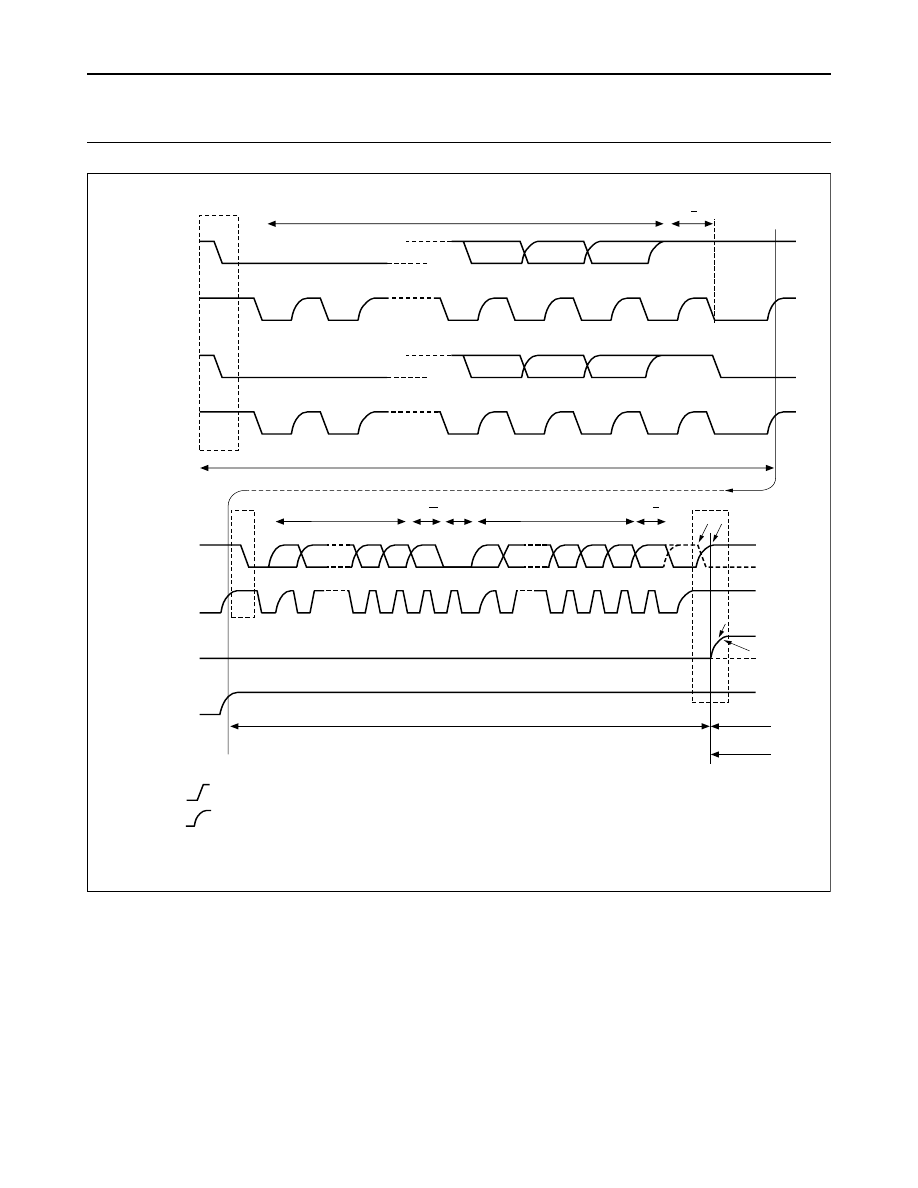
26
Philips Semiconductors
The I
2
C-bus specification
handbook, full pagewidth
MSC611
8-bit Master code 00001xxx
A
tH
t1
t2
S
F/S mode
Hs-mode
If P then
F/S mode
If Sr (dotted lines)
then Hs-mode
1
6
7
8
9
1
6
7
8
9
6
7
8
9
1
1
2 to 5
2 to 5
2 to 5
2 to 5
6
7
8
9
SDAH
SCLH
SDA
SCL
SDAH
SCLH
SDA
SCL
tH
tFS
Sr
Sr P
P
n
×
(8-bit DATA
+
A/A)
7-bit SLA
R/W
A
= MCS current source pull-up
= Rp resistor pull-up
Fig.25 A complete Hs-mode transfer in a mixed-speed bus system.
The master code is recognized by the bridge in the active
or non-active master (see Fig.24). The bridge performs the
following actions:
1.
Between t
1
and t
H
(see Fig.25), transistor TR1 opens
to separate the SDAH and SDA lines, after which
transistor TR3 closes to pull-down the SDA line to V
SS
.
2.
When both SCLH and SCL become HIGH (t
H
in
Fig.25), transistor TR2 opens to separate the SCLH
and SCL lines. TR2 must be opened before SCLH
goes LOW after Sr.
Hs-mode transfer starts after t
H
with a repeated START
condition (Sr). During Hs-mode transfer, the SCL line stays
at a HIGH and the SDA line at a LOW steady-state level,
and so is prepared for the transfer of a STOP condition (P).

27
Philips Semiconductors
The I
2
C-bus specification
After each acknowledge (A) or not-acknowledge bit (A) the
active master disables its current-source pull-up circuit.
This enables other devices to delay the serial transfer by
stretching the LOW period of the SCLH signal. The active
master re-enables its current-source pull-up circuit again
when all devices are released and the SCLH signal
reaches a HIGH level, and so speeds up the last part of the
SCLH signal’s rise time. In irregular situations, F/S-mode
devices can close the bridge (TR1 and TR2 closed, TR3
open) at any time by pulling down the SCL line for at least
1
µ
s, e.g. to recover from a bus hang-up.
Hs-mode finishes with a STOP condition and brings the
bus system back into the F/S-mode. The active master
disables its current-source MCS when the STOP condition
(P) at SDAH is detected (t
FS
in Fig.25). The bridge also
recognizes this STOP condition and takes the following
actions:
1.
Transistor TR2 closes after t
FS
to connect SCLH with
SCL; both of which are HIGH at this time. Transistor
TR3 opens after t
FS
, which releases the SDA line and
allows it to be pulled HIGH by the pull-up resister R
p
.
This is the STOP condition for the F/S-mode devices.
TR3 must open fast enough to ensure the bus free
time between the STOP condition and the earliest next
START condition is according to the Fast-mode
specification (see t
BUF
in Table 5).
2.
When SDA reaches a HIGH (t
2
in Fig.25) transistor
TR1 closes to connect SDAH with SDA. (Note:
interconnections are made when all lines are HIGH,
thus preventing spikes on the bus lines). TR1 and TR2
must be closed within the minimum bus free time
according to the Fast-mode specification (see t
BUF
in
Table 5).
13.5.3
T
IMING
REQUIREMENTS
FOR
THE
BRIDGE
IN
A
MIXED
-
SPEED
BUS
SYSTEM
It can be seen from Fig.25 that the actions of the bridge at
t
1
, t
H
and t
FS
must be so fast that it does not affect the
SDAH and SCLH lines. Furthermore the bridge must meet
the related timing requirements of the Fast-mode
specification for the SDA and SCL lines.
14 10-BIT ADDRESSING
This section describes 10-bit addressing and can be
disregarded if only 7-bit addressing is used.
10-bit addressing is compatible with, and can be combined
with, 7-bit addressing. Using 10 bits for addressing
exploits the reserved combination 1111XXX for the first
seven bits of the first byte following a START (S) or
repeated START (Sr) condition as explained in Section
10.1. The 10-bit addressing does not affect the existing
7-bit addressing. Devices with 7-bit and 10-bit addresses
can be connected to the same I
2
C-bus, and both 7-bit and
10-bit addressing can be used in F/S-mode and Hs-mode
systems.
Although there are eight possible combinations of the
reserved address bits 1111XXX, only the four
combinations 11110XX are used for 10-bit addressing.
The remaining four combinations 11111XX are reserved
for future I
2
C-bus enhancements.
14.1
Definition of bits in the first two bytes
The 10-bit slave address is formed from the first two bytes
following a START condition (S) or a repeated START
condition (Sr).
The first seven bits of the first byte are the combination
11110XX of which the last two bits (XX) are the two
most-significant bits (MSBs) of the 10-bit address; the
eighth bit of the first byte is the R/W bit that determines the
direction of the message. A ‘zero’ in the least significant
position of the first byte means that the master will write
information to a selected slave. A ‘one’ in this position
means that the master will read information from the slave.
If the R/W bit is ‘zero’, then the second byte contains the
remaining 8 bits (XXXXXXXX) of the 10-bit address. If the
R/W bit is ‘one’, then the next byte contains data
transmitted from a slave to a master.
14.2
Formats with 10-bit addresses
Various combinations of read/write formats are possible
within a transfer that includes 10-bit addressing. Possible
data transfer formats are:
•
Master-transmitter transmits to slave-receiver with a
10-bit slave address.
The transfer direction is not changed (see Fig.26). When
a 10-bit address follows a START condition, each slave
compares the first seven bits of the first byte of the slave
address (11110XX) with its own address and tests if the
eighth bit (R/W direction bit) is 0. It is possible that more
than one device will find a match and generate an
acknowledge (A1). All slaves that found a match will
compare the eight bits of the second byte of the slave
address (XXXXXXXX) with their own addresses, but
only one slave will find a match and generate an
acknowledge (A2). The matching slave will remain
addressed by the master until it receives a STOP
28
Philips Semiconductors
The I
2
C-bus specification
condition (P) or a repeated START condition (Sr)
followed by a different slave address.
•
Master-receiver reads slave- transmitter with a 10-bit
slave address.
The transfer direction is changed after the second R/W
bit (Fig.27). Up to and including acknowledge bit A2, the
procedure is the same as that described for a
master-transmitter addressing a slave-receiver. After
the repeated START condition (Sr), a matching slave
remembers that it was addressed before. This slave
then checks if the first seven bits of the first byte of the
slave address following Sr are the same as they were
after the START condition (S), and tests if the eighth
(R/W) bit is 1. If there is a match, the slave considers that
it has been addressed as a transmitter and generates
acknowledge A3. The slave-transmitter remains
addressed until it receives a STOP condition (P) or until
it receives another repeated START condition (Sr)
followed by a different slave address. After a repeated
START condition (Sr), all the other slave devices will
also compare the first seven bits of the first byte of the
slave address (11110XX) with their own addresses and
test the eighth (R/W) bit. However, none of them will be
addressed because R/W = 1 (for 10-bit devices), or the
11110XX slave address (for 7-bit devices) does not
match.
•
Combined format. A master transmits data to a slave
and then reads data from the same slave (Fig.28). The
same master occupies the bus all the time. The transfer
direction is changed after the second R/W bit.
•
Combined format. A master transmits data to one slave
and then transmits data to another slave (Fig.29). The
same master occupies the bus all the time.
•
Combined format. 10-bit and 7-bit addressing combined
in one serial transfer (Fig.30). After each START
condition (S), or each repeated START condition (Sr), a
10-bit or 7-bit slave address can be transmitted.
Figure 30 shows how a master transmits data to a slave
with a 7-bit address and then transmits data to a second
slave with a 10-bit address. The same master occupies
the bus all the time.
NOTES:
1.
Combined formats can be used, for example, to
control a serial memory. During the first data byte, the
internal memory location has to be written. After the
START condition and slave address is repeated, data
can be transferred.
2.
All decisions on auto-increment or decrement of
previously accessed memory locations etc. are taken
by the designer of the device.
3.
Each byte is followed by an acknowledgment bit as
indicated by the A or blocks in the sequence.
4.
I
2
C-bus compatible devices must reset their bus logic
on receipt of a START or repeated START condition
such that they all anticipate the sending of a slave
address.
Fig.26 A master-transmitter addresses a slave-receiver with a 10-bit address.
handbook, full pagewidth
,,
,,
,,
,,
,,
,,
,,,,
,,,,
,,,,,
,,,,,
MBC613
R/W A1
(write)
A2
A
A/A
1 1 1 1 0 X X
0
SLAVE ADDRESS
1st 7 BITS
S
DATA
P
DATA
SLAVE ADDRESS
2nd BYTE
Fig.27 A master-receiver addresses a slave-transmitter with a 10-bit address.
handbook, full pagewidth
,,
,
,,,,,
,,,,
,,,,
MBC614
R/W A1
(write)
A3 DATA
DATA
A2
R/W
(read)
1 1 1 1 0 X X
0
1 1 1 1 0 X X
1
A
A
P
Sr
SLAVE ADDRESS
1st 7 BITS
SLAVE ADDRESS
2nd BYTE
SLAVE ADDRESS
1st 7 BITS
S
29
Philips Semiconductors
The I
2
C-bus specification
Fig.28 Combined format. A master addresses a slave with a 10-bit address,
then transmits data to this slave and reads data from this slave.
handbook, full pagewidth
,,
,,
,,
,,
,,,,,
,,,,,
MBC615
(write)
A
DATA
DATA
R/W
(read)
,,
,,
,,
,,
,,,
,,,
,,,,,
,,,,,
R/W
A
A
A
A/A
1 1 1 1 0 X X
1 1 1 1 0 X X
1
0
S
SLAVE ADDRESS
1st 7 BITS
SLAVE ADDRESS
2nd BYTE
DATA
DATA
A
P
A
Sr
SLAVE ADDRESS
1st 7 BITS
handbook, full pagewidth
,,
,,
,,
,,
,,
,,
,,,,
,,,,
,,,,,
,,,,,
MBC616
(write)
A
A
A/A
(write)
A
,,
,,
,,
,,
,,,,
,,,,
,,,,,
,,,,,
A
A
A
A/A
1 1 1 1 0 X X
1 1 1 1 0 X X
0
0
S
SLAVE ADDRESS
1st 7 BITS
R/W
SLAVE ADDRESS
2nd BYTE
DATA
DATA
Sr
SLAVE ADDRESS
1st 7 BITS
R/W
2nd BYTE
SLAVE ADDRESS
DATA
P
DATA
Fig.29 Combined format. A master transmits data to two slaves, both with 10-bit addresses.
Fig.30 Combined format. A master transmits data to two slaves, one with a 7-bit address,
and one with a 10-bit address.
dbook, full pagewidth
,,
,,
,,
,,
,
,
,,,,
,,,,
,,,,,
,,,,,
,,
,,
,,,,
,,,,
,,
,,
MBC617
R/W
A
(write)
A
A
A/A
R/W
(write)
A
A/A
A
1 1 1 1 0 X X
0
0
S
SLAVE ADDRESS
7 - BIT
DATA
DATA
DATA
DATA
P
SLAVE ADDRESS
1st 7 BITS OF 10-BIT
Sr
SLAVE ADDRESS
2nd BYTE OF 10-BIT

30
Philips Semiconductors
The I
2
C-bus specification
14.3
General call address and start byte with 10-bit
addressing
The 10-bit addressing procedure for the I
2
C-bus is such
that the first two bytes after the START condition (S)
usually determine which slave will be selected by the
master. The exception is the “general call” address
00000000 (H‘00’). Slave devices with 10-bit addressing
will react to a “general call” in the same way as slave
devices with 7-bit addressing (see Section 10.1.1).
Hardware masters can transmit their 10-bit address after a
‘general call’. In this case, the ‘general call’ address byte is
followed by two successive bytes containing the 10-bit
address of the master-transmitter. The format is as shown
in Fig.10 where the first DATA byte contains the eight
least-significant bits of the master address.
The START byte 00000001 (H‘01’) can precede the 10-bit
addressing in the same way as for 7-bit addressing (see
Section 10.1.2).
15 ELECTRICAL SPECIFICATIONS AND TIMING FOR
I/O STAGES AND BUS LINES
15.1
Standard- and Fast-mode devices
The I/O levels, I/O current, spike suppression, output slope
control and pin capacitance for F/S-mode I
2
C-bus devices
are given in Table 4. The I
2
C-bus timing characteristics,
bus-line capacitance and noise margin are given in
Table 5. Figure 31 shows the timing definitions for the
I
2
C-bus.
The minimum HIGH and LOW periods of the SCL clock
specified in Table 5 determine the maximum bit transfer
rates of 100 kbit/s for Standard-mode devices and
400 kbit/s for Fast-mode devices. Standard-mode and
Fast-mode I
2
C-bus devices must be able to follow
transfers at their own maximum bit rates, either by being
able to transmit or receive at that speed or by applying the
clock synchronization procedure described in Section 8
which will force the master into a wait state and stretch the
LOW period of the SCL signal. Of course, in the latter case
the bit transfer rate is reduced.
31
Philips Semiconductors
The I
2
C-bus specification
Table 4
Characteristics of the SDA and SCL I/O stages for F/S-mode I
2
C-bus devices
Notes
1.
Devices that use non-standard supply voltages which do not conform to the intended I
2
C-bus system levels must
relate their input levels to the V
DD
voltage to which the pull-up resistors R
p
are connected.
2.
Maximum V
IH
= V
DDmax
+ 0.5 V.
3.
C
b
= capacitance of one bus line in pF.
4.
The maximum t
f
for the SDA and SCL bus lines quoted in Table 5 (300 ns) is longer than the specified maximum t
of
for the output stages (250 ns). This allows series protection resistors (R
s
) to be connected between the SDA/SCL
pins and the SDA/SCL bus lines as shown in Fig.36 without exceeding the maximum specified t
f
.
5.
I/O pins of Fast-mode devices must not obstruct the SDA and SCL lines if V
DD
is switched off.
n/a = not applicable
PARAMETER
SYMBOL
STANDARD-MODE
FAST-MODE
UNIT
MIN.
MAX.
MIN.
MAX.
LOW level input voltage:
fixed input levels
V
DD
-related input levels
V
IL
−
0.5
−
0.5
1.5
0.3V
DD
n/a
−
0.5
n/a
0.3V
DD
(1)
V
V
HIGH level input voltage:
fixed input levels
V
DD
-related input levels
V
IH
3.0
0.7V
DD
(2)
(2)
n/a
0.7V
DD
(1)
n/a
(2)
V
V
Hysteresis of Schmitt trigger inputs:
V
DD
> 2 V
V
DD
< 2 V
V
hys
n/a
n/a
n/a
n/a
0.05V
DD
0.1V
DD
–
–
V
V
LOW level output voltage (open drain or
open collector) at 3 mA sink current:
V
DD
> 2 V
V
DD
< 2 V
V
OL1
V
OL3
0
n/a
0.4
n/a
0
0
0.4
0.2V
DD
V
V
Output fall time from V
IHmin
to V
ILmax
with
a bus capacitance from 10 pF to 400 pF
t
of
–
250
(4)
20 + 0.1C
b
(3)
250
(4)
ns
Pulse width of spikes which must be
suppressed by the input filter
t
SP
n/a
n/a
0
50
ns
Input current each I/O pin with an input
voltage between 0.1V
DD
and 0.9V
DDmax
I
i
−
10
10
−
10
(5)
10
(5)
µ
A
Capacitance for each I/O pin
C
i
−
10
−
10
pF
32
Philips Semiconductors
The I
2
C-bus specification
Table 5
Characteristics of the SDA and SCL bus lines for F/S-mode I
2
C-bus devices
(1)
Notes
1.
All values referred to V
IHmin
and V
ILmax
levels (see Table 4).
2.
A device must internally provide a hold time of at least 300 ns for the SDA signal (referred to the V
IHmin
of the SCL
signal) to bridge the undefined region of the falling edge of SCL.
3.
The maximum t
HD;DAT
has only to be met if the device does not stretch the LOW period (t
LOW
) of the SCL signal.
4.
A Fast-mode I
2
C-bus device can be used in a Standard-mode I
2
C-bus system, but the requirement t
SU;DAT
≥
250 ns
must then be met. This will automatically be the case if the device does not stretch the LOW period of the SCL signal.
If such a device does stretch the LOW period of the SCL signal, it must output the next data bit to the SDA line t
r max
+ t
SU;DAT
= 1000 + 250 = 1250 ns (according to the Standard-mode I
2
C-bus specification) before the SCL line is
released.
5.
C
b
= total capacitance of one bus line in pF. If mixed with Hs-mode devices, faster fall-times according to Table 6 are
allowed.
n/a = not applicable
PARAMETER
SYMBOL
STANDARD-MODE
FAST-MODE
UNIT
MIN.
MAX.
MIN.
MAX.
SCL clock frequency
f
SCL
0
100
0
400
kHz
Hold time (repeated) START condition.
After this period, the first clock pulse is
generated
t
HD;STA
4.0
–
0.6
−
µ
s
LOW period of the SCL clock
t
LOW
4.7
–
1.3
–
µ
s
HIGH period of the SCL clock
t
HIGH
4.0
–
0.6
–
µ
s
Set-up time for a repeated START
condition
t
SU;STA
4.7
–
0.6
–
µ
s
Data hold time:
for CBUS compatible masters (see NOTE,
Section 10.1.3)
for I
2
C-bus devices
t
HD;DAT
5.0
0
(2)
–
3.45
(3)
–
0
(2)
–
0.9
(3)
µ
s
µ
s
Data set-up time
t
SU;DAT
250
−
100
(4)
–
ns
Rise time of both SDA and SCL signals
t
r
–
1000
20 + 0.1C
b
(5)
300
ns
Fall time of both SDA and SCL signals
t
f
–
300
20 + 0.1C
b
(5)
300
ns
Set-up time for STOP condition
t
SU;STO
4.0
–
0.6
–
µ
s
Bus free time between a STOP and
START condition
t
BUF
4.7
–
1.3
–
µ
s
Capacitive load for each bus line
C
b
–
400
–
400
pF
Noise margin at the LOW level for each
connected device (including hysteresis)
V
nL
0.1V
DD
–
0.1V
DD
–
V
Noise margin at the HIGH level for each
connected device (including hysteresis)
V
nH
0.2V
DD
–
0.2V
DD
–
V
33
Philips Semiconductors
The I
2
C-bus specification
Fig.31 Definition of timing for F/S-mode devices on the I
2
C-bus.
handbook, full pagewidth
MSC610
S
Sr
tSU;STO
tSU;STA
tHD;STA
tHIGH
tLOW
tSU;DAT
tHD;DAT
tf
SDA
SCL
P
S
tBUF
tr
tf
tr
tSP
tHD;STA

34
Philips Semiconductors
The I
2
C-bus specification
15.2
Hs-mode devices
The I/O levels, I/O current, spike suppression, output slope
control and pin capacitance for I
2
C-bus Hs-mode devices
are given in Table 6. The noise margin for HIGH and LOW
levels on the bus lines are the same as specified for
F/S-mode I
2
C-bus devices.
Figure 32 shows all timing parameters for the Hs-mode
timing.The “normal” START condition S does not exist in
Hs-mode. Timing parameters for Address bits, R/W bit,
Acknowledge bit and DATA bits are all the same. Only the
rising edge of the first SCLH clock signal after an
acknowledge bit has an larger value because the external
R
p
has to pull-up SCLH without the help of the internal
current-source.
The Hs-mode timing parameters for the bus lines are
specified in Table 7. The minimum HIGH and LOW periods
and the maximum rise and fall times of the SCLH clock
signal determine the highest bit rate.
With an internally generated SCLH signal with LOW and
HIGH level periods of 200 ns and 100 ns respectively, an
Hs-mode master can fulfil the timing requirements for the
external SCLH clock pulses (taking the rise and fall times
into account) for the maximum bit rate of 3.4 Mbit/s. So a
basic frequency of 10 MHz, or a multiple of 10 MHz, can
be used by an Hs-mode master to generate the SCLH
signal. There are no limits for maximum HIGH and LOW
periods of the SCLH clock, and there is no limit for a lowest
bit rate.
Timing parameters are independent for capacitive load up
to 100 pF for each bus line allowing the maximum possible
bit rate of 3.4 Mbit/s. At a higher capacitive load on the bus
lines, the bit rate decreases gradually. The timing
parameters for a capacitive bus load of 400 pF are
specified in Table 7, allowing a maximum bit rate of
1.7 Mbit/s. For capacitive bus loads between 100 pF and
400 pF, the timing parameters must be interpolated
linearly. Rise and fall times are in accordance with the
maximum propagation time of the transmission lines
SDAH and SCLH to prevent reflections of the open ends.
35
Philips Semiconductors
The I
2
C-bus specification
Table 6
Characteristics of the SDAH, SCLH, SDA and SCL I/O stages for Hs-mode I
2
C-bus devices
Notes
1.
Devices that use non-standard supply voltages which do not conform to the intended I
2
C-bus system levels must
relate their input levels to the V
DD
voltage to which the pull-up resistors R
p
are connected.
2.
Devices that offer the level shift function must tolerate a maximum input voltage of 5.5 V at SDA and SCL.
3.
For capacitive bus loads between 100 and 400 pF, the rise and fall time values must be linearly interpolated.
4.
SDAH and SCLH I/O stages of Hs-mode slave devices must have floating outputs if their supply voltage has been
switched off. Due to the current-source output circuit, which normally has a clipping diode to V
DD
, this requirement is
not mandatory for the SCLH or the SDAH I/O stage of Hs-mode master devices. This means that the supply voltage
of Hs-mode master devices cannot be switched off without affecting the SDAH and SCLH lines.
PARAMETER
SYMBOL
Hs-MODE
UNIT
MIN.
MAX.
LOW level input voltage
V
IL
−
0.5
0.3V
DD
(1)
V
HIGH level input voltage
V
IH
0.7V
DD
(1)
V
DD
+ 0.5
(2)
V
Hysteresis of Schmitt trigger inputs
V
hys
0.1V
DD
(1)
–
V
LOW level output voltage (open drain) at 3 mA sink
current at SDAH, SDA and SCLH for:
V
DD
> 2 V
V
DD
< 2 V
V
OL
0
0
0.4
0.2V
DD
V
V
On resistance of the transfer gate, for both current
directions at V
OL
level between SDA and SDAH or
SCL and SCLH at 3 mA
R
onL
−
50
Ω
On resistance of the transfer gate between SDA and
SDAH or SCL and SCLH if both are at V
DD
level
R
onH
(2)
50
–
k
Ω
Pull-up current of the SCLH current-source. Applies for
SCLH output levels between 0.3V
DD
and 0.7V
DD
I
CS
3
12
mA
Output rise time (current-source enabled) and fall time
at SCLH with a capacitive load from 10 to 100 pF
t
rCL
, t
fCL
10
40
ns
Output rise time (current-source enabled) and fall time
at SCLH with an external pull-up current source of 3 mA
and a capacitive load of 400 pF
t
rCL
(3)
, t
fCL
(3)
20
80
ns
Output fall time at SDAH with a capacitive load from 10
to 100 pF
t
fDA
10
80
ns
Output fall time at SDAH with a capacitive load of
400 pF
t
fDA
(3)
20
160
ns
Pulse width of spikes at SDAH and SCLH that must be
suppressed by the input filters
t
SP
0
10
ns
Input current each I/O pin with an input voltage between
0.1V
DD
and 0.9V
DD
I
i
(4)
–
10
µ
A
Capacitance for each I/O pin
C
i
–
10
pF
36
Philips Semiconductors
The I
2
C-bus specification
Table 7
Characteristics of the SDAH, SCLH, SDA and SCL bus lines for Hs-mode I
2
C-bus devices
(1)
Notes
1.
All values referred to V
IHmin
and V
ILmax
levels (see Table 6).
2.
For bus line loads C
b
between 100 and 400 pF the timing parameters must be linearly interpolated.
3.
A device must internally provide a Data hold time to bridge the undefined part between V
IH
and V
IL
of the falling edge
of the SCLH signal. An input circuit with a threshold as low as possible for the falling edge of the SCLH signal
minimizes this hold time.
PARAMETER
SYMBOL
C
b
= 100 pF MAX.
C
b
= 400 pF
(2)
UNIT
MIN.
MAX.
MIN.
MAX.
SCLH clock frequency
f
SCLH
0
3.4
0
1.7
MHz
Set-up time (repeated) START condition
t
SU;STA
160
−
160
−
ns
Hold time (repeated) START condition
t
HD;STA
160
−
160
−
ns
LOW period of the SCLH clock
t
LOW
160
−
320
−
ns
HIGH period of the SCLH clock
t
HIGH
60
−
120
−
ns
Data set-up time
t
SU;DAT
10
−
10
−
ns
Data hold time
t
HD;DAT
0
(3)
70
0
(3)
150
ns
Rise time of SCLH signal
t
rCL
10
40
20
80
ns
Rise time of SCLH signal after a repeated
START condition and after an
acknowledge bit
t
rCL1
10
80
20
160
ns
Fall time of SCLH signal
t
fCL
10
40
20
80
ns
Rise time of SDAH signal
t
rDA
10
80
20
160
ns
Fall time of SDAH signal
t
fDA
10
80
20
160
ns
Set-up time for STOP condition
t
SU;STO
160
−
160
−
ns
Capacitive load for SDAH and SCLH lines
C
b
(2)
−
100
−
400
pF
Capacitive load for SDAH + SDA line and
SCLH + SCL line
C
b
−
400
−
400
pF
Noise margin at the LOW level for each
connected device (including hysteresis)
V
nL
0.1V
DD
−
0.1V
DD
−
V
Noise margin at the HIGH level for each
connected device (including hysteresis)
V
nH
0.2V
DD
−
0.2V
DD
−
V
37
Philips Semiconductors
The I
2
C-bus specification
Fig.32 Definition of timing for Hs-mode devices on the I
2
C-bus.
(1) First rising edge of the SCLH signal after Sr and after each acknowledge bit.
handbook, full pagewidth
MGK871
SDAH
Sr
Sr
P
SCLH
= MCS current source pull-up
= Rp resistor pull-up
tfDA
trDA
tHD;STA
tSU;DAT
trCL
tLOW
tHIGH
tHD;DAT
tLOW
tHIGH
trCL1
tfCL
tSU;STO
trCL1
(1)
(1)
tSU;STA
16 ELECTRICAL CONNECTIONS OF I
2
C-BUS
DEVICES TO THE BUS LINES
The electrical specifications for the I/Os of I
2
C-bus devices
and the characteristics of the bus lines connected to them
are given in Section 15.
I
2
C-bus devices with fixed input levels of 1.5 V and 3 V can
each have their own appropriate supply voltage. Pull-up
resistors must be connected to a 5 V
±
10% supply
(Fig.33). I
2
C-bus devices with input levels related to V
DD
must have one common supply line to which the pull-up
resistor is also connected (Fig.34).
When devices with fixed input levels are mixed with
devices with input levels related to V
DD
, the latter devices
must be connected to one common supply line of
5 V
±
10% and must have pull-up resistors connected to
their SDA and SCL pins as shown in Fig.35.
New Fast- and Hs-mode devices must have supply voltage
related input levels as specified in Tables 4 and 6.
Input levels are defined in such a way that:
•
The noise margin on the LOW level is 0.1V
DD
•
The noise margin on the HIGH level is 0.2V
DD
•
As shown in Fig.36, series resistors (R
S
) of e.g. 300
Ω
can be used for protection against high-voltage spikes
on the SDA and SCL lines (resulting from the flash-over
of a TV picture tube, for example).
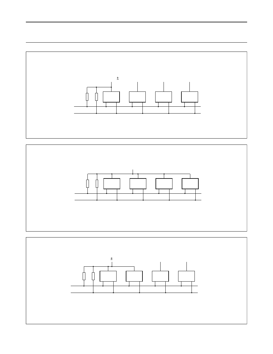
38
Philips Semiconductors
The I
2
C-bus specification
Fig.33 Fixed input level devices connected to the I
2
C-bus.
handbook, full pagewidth
MBC610
SDA
SCL
R p
NMOS
VDD1
R p
BiCMOS
VDD2
CMOS
VDD3
BIPOLAR
VDD4
= 5 V 10 %
DD2 - 4
V
are device dependent (e.g. 12 V)
Fig.34 Devices with wide supply voltage range connected to the I
2
C-bus.
handbook, full pagewidth
MBC625
SDA
SCL
R p
R p
CMOS
CMOS
CMOS
CMOS
V DD = e.g. 3 V
Fig.35 Devices with input levels related to V
DD
(supply V
DD1
) mixed with fixed input level devices
(supply V
DD2,3
) on the I
2
C-bus.
handbook, full pagewidth
MBC626
SDA
SCL
R p
CMOS
R p
CMOS
NMOS
BIPOLAR
5 V 10 %
VDD1 =
V DD2
VDD3
VDD2,3 are device dependent (e.g. 12 V)
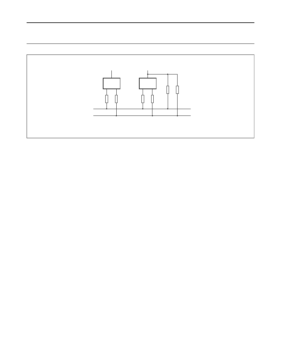
39
Philips Semiconductors
The I
2
C-bus specification
Fig.36 Series resistors (R
s
) for protection against high-voltage spikes.
handbook, full pagewidth
MBC627
SDA
SCL
Rp
Rp
DEVICE
V DD
I C
2
Rs
Rs
DEVICE
V DD
I C
2
Rs
Rs
16.1
Maximum and minimum values of resistors R
p
and R
s
for Standard-mode I
2
C-bus devices
For Standard-mode I
2
C-bus systems, the values of
resistors R
p
and R
s
in Fig.33 depend on the following
parameters:
•
Supply voltage
•
Bus capacitance
•
Number of connected devices (input current + leakage
current).
The supply voltage limits the minimum value of resistor R
p
due to the specified minimum sink current of 3 mA at
V
OLmax
= 0.4 V for the output stages. V
DD
as a function of
R
p min
is shown in Fig.37. The required noise margin of
0.1V
DD
for the LOW level, limits the maximum value of R
s
.
R
s max
as a function of R
p
is shown in Fig.38.
The bus capacitance is the total capacitance of wire,
connections and pins. This capacitance limits the
maximum value of R
p
due to the specified rise time. Fig.39
shows R
p max
as a function of bus capacitance.
The maximum HIGH level input current of each
input/output connection has a specified maximum value of
10
µ
A. Due to the required noise margin of 0.2 V
DD
for the
HIGH level, this input current limits the maximum value of
R
p
. This limit depends on V
DD
. The total HIGH level input
current is shown as a function of R
p max
in Fig.40.
40
Philips Semiconductors
The I
2
C-bus specification
Fig.37 Minimum value of R
p
as a function of supply
voltage with the value os R
s
as a parameter.
handbook, halfpage
0
4
8
16
6
0
2
4
MBC628
12
minimum
value R p
(k )
Ω
V (V)
DD
5
3
1
R = 0
S
max. R S
0
400
800
1600
10
0
8
MBC629
1200
6
4
2
maximum value R (
Ω
)
s
15 V
10 V
R p
(k )
Ω
V = 2.5 V
DD
5 V
Fig.38 Maximum value of R
s
as a function of the
value of R
p
with supply voltage as a parameter.
Fig.39 Maximum value of R
p
as a function of bus
capacitance for a Standard-mode I
2
C-bus.
0
100
200
400
20
0
16
MBC635
300
12
8
4
bus capacitance (pF)
maximum
value R
(k
Ω
)
p
max. R
@ VDD= 5 V
S
R = 0
S
Fig.40 Total HIGH level input current as a function
of the maximum value of R
p
with supply voltage as
a parameter.
0
200
20
0
4
MBC630
8
12
16
40
80
120
160
total high level input current (
µ
A)
maximum
value R p
(k )
Ω
5 V
V = 15 V
DD
2.5 V
10 V
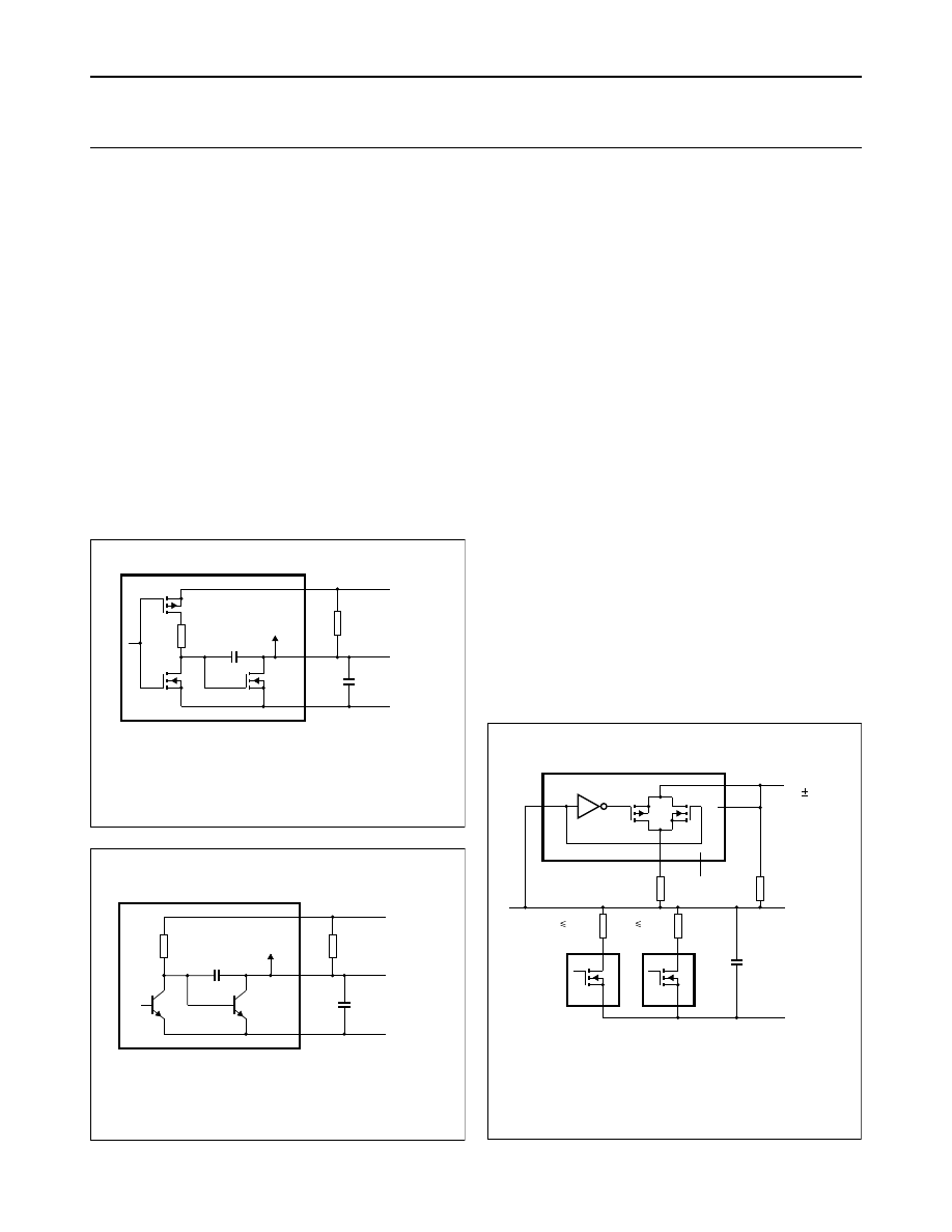
41
Philips Semiconductors
The I
2
C-bus specification
17 APPLICATION INFORMATION
17.1
Slope-controlled output stages of Fast-mode
I
2
C-bus devices
The electrical specifications for the I/Os of I
2
C-bus devices
and the characteristics of the bus lines connected to them
are given in Section 15.
Figures 41 and 42 show examples of output stages with
slope control in CMOS and bipolar technology. The slope
of the falling edge is defined by a Miller capacitor (C1) and
a resistor (R1). The typical values for C1 and R1 are
indicated on the diagrams. The wide tolerance for output
fall time t
of
given in Table 4 means that the design is not
critical. The fall time is only slightly influenced by the
external bus load (C
b
) and external pull-up resistor (R
p
).
However, the rise time (t
r
) specified in Table 5 is mainly
determined by the bus load capacitance and the value of
the pull-up resistor.
17.2
Switched pull-up circuit for Fast-mode I
2
C-bus
devices
The supply voltage (V
DD
) and the maximum output LOW
level determine the minimum value of pull-up resistor R
p
(see Section 16.1). For example, with a supply voltage of
V
DD
= 5 V
±
10% and V
OLmax
= 0.4 V at 3 mA, R
p min
=
(5.5
−
0.4)/0.003 = 1.7 k
Ω
. As shown in Fig.33, this value
of R
p
limits the maximum bus capacitance to about 200 pF
to meet the maximum t
r
requirement of 300 ns. If the bus
has a higher capacitance than this, a switched pull-up
circuit as shown in Fig.43 can be used.
The switched pull-up circuit in Fig.43 is for a supply voltage
of V
DD
= 5 V
±
10% and a maximum capacitive load of
400 pF. Since it is controlled by the bus levels, it needs no
additional switching control signals. During the
rising/falling edges, the bilateral switch in the HCT4066
switches pull-up resistor R
p2
on/off at bus levels between
0.8 V and 2.0 V. Combined resistors R
p1
and R
p2
can
pull-up the bus line within the maximum specified rise time
(t
r
) of 300 ns.
Series resistors R
s
are optional. They protect the I/O
stages of the I
2
C-bus devices from high-voltage spikes on
the bus lines, and minimize crosstalk and undershoot of
the bus line signals. The maximum value of R
s
is
determined by the maximum permitted voltage drop
across this resistor when the bus line is switched to the
LOW level in order to switch off R
p2
.
Fig.41 Slope-controlled output stage in CMOS
technology.
MBC618
P1
N1
R1
50 k
Ω
N2
2 pF
to input
circuit
C1
VDD
I/O
VSS
R p
C b
VDD
VSS
SDA or SCL
bus line
Fig.42 Slope-controlled output stage in bipolar
technology.
MBC619
R1
20 k
Ω
to input
circuit
5 pF
C1
I/O
R p
C b
VDD
VSS
Vp
GND
T1
T2
SDA or SCL
bus line
Fig.43 Switched pull-up circuit.
MBC620
1.3 k
Ω
VCC
I/O
Cb
VDD
VSS
SDA or SCL
bus line
N
P
1/4 HCT4066
nZ
GND
nE
nY
5V 10 %
Rp2
1.7 k
Ω
R p1
100
Ω
R s
N
I/O
100
Ω
R s
N
400 pF
max.
FAST - MODE I C BUS DEVICES
2
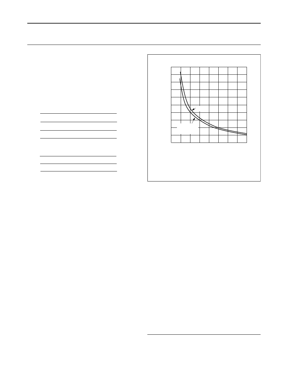
42
Philips Semiconductors
The I
2
C-bus specification
17.3
Wiring pattern of the bus lines
In general, the wiring must be so chosen that crosstalk and
interference to/from the bus lines is minimized. The bus
lines are most susceptible to crosstalk and interference at
the HIGH level because of the relatively high impedance of
the pull-up devices.
If the length of the bus lines on a PCB or ribbon cable
exceeds 10 cm and includes the V
DD
and V
SS
lines, the
wiring pattern must be:
SDA
V
DD
V
SS
SCL
If only the V
SS
line is included, the wiring pattern must be:
SDA
V
SS
SCL
These wiring patterns also result in identical capacitive
loads for the SDA and SCL lines. The V
SS
and V
DD
lines
can be omitted if a PCB with a V
SS
and/or V
DD
layer is
used.
If the bus lines are twisted-pairs, each bus line must be
twisted with a V
SS
return. Alternatively, the SCL line can be
twisted with a V
SS
return, and the SDA line twisted with a
V
DD
return. In the latter case, capacitors must be used to
decouple the V
DD
line to the V
SS
line at both ends of the
twisted pairs.
If the bus lines are shielded (shield connected to V
SS
),
interference will be minimized. However, the shielded
cable must have low capacitive coupling between the SDA
and SCL lines to minimize crosstalk.
17.4
Maximum and minimum values of resistors R
p
and R
s
for Fast-mode I
2
C-bus devices
The maximum and minimum values for resistors R
p
and R
s
connected to a Fast-mode I
2
C-bus can be determined
from Figs 37, 38 and 40 in Section 16.1. Because a
Fast-mode I
2
C-bus has faster rise times (t
r
) the maximum
value of R
p
as a function of bus capacitance is less than
that shown in Fig.39 The replacement graph for Fig.39
showing the maximum value of R
p
as a function of bus
capacitance (C
b
) for a Fast-mode I
2
C-bus is given in
Fig.44.
17.5
Maximum and minimum values of resistors R
p
and R
s
for Hs-mode I
2
C-bus devices
The maximum and minimum values for resistors R
p
and R
s
connected to an Hs-mode I
2
C-bus can be calculated from
the data in Tables 6 and 7. Many combinations of these
values are possible, owing to different rise and fall times,
bus line loads, supply voltages, mixed speed systems and
level shifting. Because of this, no further graphs are
included in this specification.
18 BI-DIRECTIONAL LEVEL SHIFTER FOR F/S-MODE
I
2
C-BUS SYSTEMS
Present technology processes for integrated circuits with
clearances of 0.5
µ
m and less limit the maximum supply
voltage and consequently the logic levels for the digital I/O
signals. To interface these lower voltage circuits with
existing 5 V devices, a level shifter is needed. For
bi-directional bus systems like the I
2
C-bus, such a level
shifter must also be bi-directional, without the need of a
direction control signal
(1)
. The simplest way to solve this
problem is by connecting a discrete MOS-FET to each bus
line.
(1) US 5,689,196 granted; corresponding patent applications
pending.
Fig.44 Maximum value of R
p
as a function of bus
capacitance for meeting the t
r max
requirement for
a Fast-mode I
2
C-bus.
handbook, halfpage
0
100
200
400
7.5
0
6.0
MBC612
300
4.5
3.0
1.5
bus capacitance (pF)
maximum
value R
(k
Ω
)
p
max. R
@ VDD= 5 V
S
R = 0
S
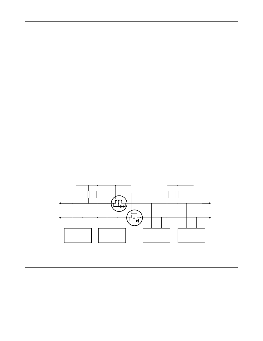
43
Philips Semiconductors
The I
2
C-bus specification
In spite of its surprising simplicity, such a solution not only
fulfils the requirement of bi-directional level shifting without
a direction control signal, it also:
•
isolates a powered-down bus section from the rest of the
bus system
•
protects the “lower voltage” side against high voltage
spikes from the “higher-voltage” side.
The bi-directional level shifter can be used for both
Standard-mode (up to100 kbit/s) or in Fast-mode (up to
400 kbit/s) I
2
C-bus systems. It is not intended for Hs-mode
systems, which may have a bridge with a level shifting
possibility (see Section 13.5)
18.1
Connecting devices with different logic levels
Section 16 described how different voltage devices could
be connected to the same bus by using pull-up resistors to
the supply voltage line. Although this is the simplest
solution, the lower voltage devices must be 5 V tolerant,
which can make them more expensive to manufacture. By
using a bi-directional level shifter, however, it’s possible to
interconnect two sections of an I
2
C-bus system, with each
section having a different supply voltage and different logic
levels. Such a configuration is shown in Fig.45. The left
“low-voltage” section has pull-up resistors and devices
connected to a 3.3 V supply voltage, the right
“high-voltage” section has pull-up resistors and devices
connected to a 5 V supply voltage. The devices of each
section have I/Os with supply voltage related logic input
levels and an open drain output configuration.
The level shifter for each bus line is identical and consists
of one discrete N-channel enhancement MOS-FET; TR1
for the serial data line SDA and TR2 for the serial clock line
SCL. The gates (g) have to be connected to the lowest
supply voltage V
DD1
, the sources (s) to the bus lines of the
“lower-voltage” section, and the drains (d) to the bus lines
of the “higher-voltage” section. Many MOS-FETs have the
substrate internally connected with its source, if this is not
the case, an external connection should be made. Each
MOS-FET has an integral diode (n-p junction) between the
drain and substrate.
Fig.45 Bi-directional level shifter circuit connecting two different voltage sections in an I
2
C-bus system.
handbook, full pagewidth
MGK879
3.3 V DEVICE
3.3 V DEVICE
5 V DEVICE
5 V DEVICE
g
s
d
g
s
d
TR1
TR2
VDD2 = 5 V
SDA2
SCL2
VDD1 = 3.3 V
SDA1
SCL1
Rp
Rp
Rp
Rp

44
Philips Semiconductors
The I
2
C-bus specification
18.1.1
O
PERATION
OF
THE
LEVEL
SHIFTER
The following three states should be considered during the
operation of the level shifter:
1.
No device is pulling down the bus line.
The bus line of the “lower-voltage” section is pulled up
by its pull-up resistors R
p
to 3.3 V. The gate and the
source of the MOS-FET are both at 3.3 V, so its V
GS
is
below the threshold voltage and the MOS-FET is not
conducting. This allows the bus line at the
“higher-voltage” section to be pulled up by its pull-up
resistor R
p
to 5 V. So the bus lines of both sections are
HIGH, but at a different voltage level.
2.
A 3.3 V device pulls down the bus line to a LOW level.
The source of the MOS-FET also becomes LOW,
while the gate stay at 3.3 V. V
GS
rises above the
threshold and the MOS-FET starts to conduct. The bus
line of the “higher-voltage” section is then also pulled
down to a LOW level by the 3.3 V device via the
conducting MOS-FET. So the bus lines of both
sections go LOW to the same voltage level.
3.
A 5 V device pulls down the bus line to a LOW level.
The drain-substrate diode of the MOS-FET the
“lower-voltage” section is pulled down until V
GS
passes the threshold and the MOS-FET starts to
conduct. The bus line of the “lower-voltage” section is
then further pulled down to a LOW level by the 5 V
device via the conducting MOS-FET. So the bus lines
of both sections go LOW to the same voltage level.
The three states show that the logic levels are transferred
in both directions of the bus system, independent of the
driving section. State 1 performs the level shift function.
States 2 and 3 perform a “wired AND” function between
the bus lines of both sections as required by the I
2
C-bus
specification.
Supply voltages other than 3.3 V for V
DD1
and 5 V for V
DD2
can also be applied, e.g. 2 V for V
DD1
and 10 V for V
DD2
is
feasible. In normal operation V
DD2
must be equal to or
higher than V
DD1
(V
DD2
is allowed to fall below V
DD1
during
switching power on/off).
45
Philips Semiconductors
The I
2
C-bus specification
19 DEVELOPMENT TOOLS AVAILABLE FROM PHILIPS
Table 8
I
2
C evaluation boards
Table 9
Development tools for 80C51-based systems
Table 10 Development tools for 68000-based systems
Table 11 I
2
C analyzers
PRODUCT
DESCRIPTION
OM4151/
S87C00KSD
I
2
C-bus evaluation board with microcontroller, LCD, LED, Par. I/O, SRAM, EEPROM, Clock, DTMF
generator, AD/DA conversion.
OM5500
Demo kit for the PCF2166 LCD driver and PCD3756A telecom microcontroller
PRODUCT
DESCRIPTION
PDS51
A board-level, full featured, in-circuit emulator:
RS232 interface to PC, universal motherboard, controlled via terminal emulation
PRODUCT
DESCRIPTION
OM4160/2
Microcore-2 demonstration/evaluation board with SCC68070
OM4160/4
Microcore-4 demonstration/evaluation board with 90CE201
OM4160/5
Microcore-5 demonstration/evaluation board with 90CE301
PRODUCT
DESCRIPTION
OM1022
PC I
2
C-bus analyzer with multi-master capability. Hardware and software (runs on IBM or
compatible PC) to experiment with and analyze the behaviour of the I
2
C-bus (includes
documentation)
OM4777
Similar to OM1022 but for single-master systems only
PF8681
I
2
C-bus analyzer support package for the PM3580 logic analyzer family
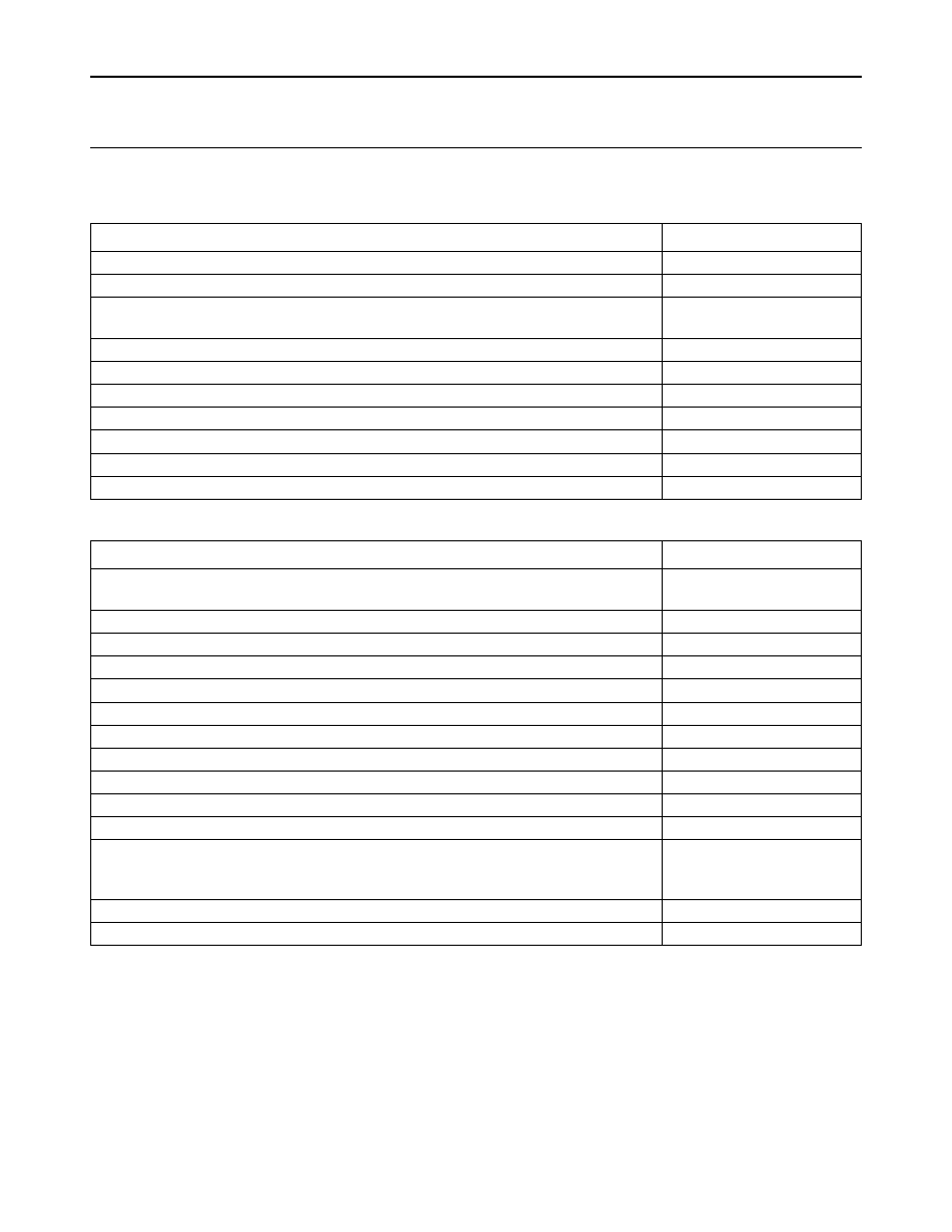
46
Philips Semiconductors
The I
2
C-bus specification
20 SUPPORT LITERATURE
Table 12 Data handbooks
Table 13 Brochures/leaflets/lab. reports/books etc.
For more information about Philips Semiconductors and how we can help with your I
2
C-bus design, contact your nearest
Philips Semiconductors national organization from the address list of the back of this book, or visit our worldwide web
site at http://www.semiconductors.philips.com/i2c for the latest products, news and applications notes.
TITLE
ORDERING CODE
IC01: Semiconductors for Radio, Audio and CD/DVD Systems
9397 750 02453
IC02: Semiconductors for Television and Video Systems
9397 750 01989
IC03: Semiconductors for Wired Telecom Systems (parts a & b)
9397 750 00839,
9397 750 00811
IC12: I
2
C Peripherals
9397 750 01647
IC14: 8048-based 8-bit microcontrollers
9398 652 40011
IC17: Semiconductors for wireless communications
9397 750 01002
IC18: Semiconductors for in-car electronics
9397 750 00418
IC19: ICs for data communications
9397 750 00138
IC20: 80C51-based 8-bit microcontrollers + Application notes and Development tools
9397 750 00963
IC22: Multimedia ICs
9397 750 02183
TITLE
ORDERING CODE
Can you make the distance... with I
2
C-bus (information about the P82B715 I
2
C-bus
extender IC)
9397 750 00008
I
2
C-bus multi-master & single-master controller kits
9397 750 00953
Desktop video (CD-ROM)
9397 750 00644
80C51 core instructions quick reference
9398 510 76011
80C51 microcontroller selection guide
9397 750 01587
OM5027 I
2
C-bus evaluation board for low-voltage, low-power ICs & software
9398 706 98011
P90CL301 I
2
C driver routines
AN94078
User manual of Microsoft Pascal I
2
C-bus driver (MICDRV4.OBJ)
ETV/IR8833
C routines for the PCF8584
AN95068
Using the PCF8584 with non-specified timings and other frequently asked questions
AN96040
User's guide to I
2
C-bus control programs
ETV8835
The I
2
C-bus from theory to practice (book and disk)
Author: D. Paret
Publisher: Wiley
ISBN: 0-471-96268-6
Bi-directional level shifter for I
2
C-bus and other systems
AN97055
OM5500 demo kit for the PCF2166 LCD driver and PCD3756A telecom microcontroller 9397 750 00954
Wyszukiwarka
Podobne podstrony:
IC zamienniki eu ru tomsk id 20 Nieznany
how to write great essays id 20 Nieznany
HPS5 oscyloskop osobisty id 20 Nieznany
Herbaty przeciwutleniacze id 20 Nieznany
Historia mediow zajecia 1 id 20 Nieznany
II Rzymski proces cywilny id 20 Nieznany
jonh hopkins pol 2000 id 228521 Nieznany
holelarstwo cw kolokwium id 20 Nieznany
I2C BUS SPECIFICATION 2
IC zamienniki eu ru tomsk id 20 Nieznany
how to write great essays id 20 Nieznany
I2C BUS SPECIFICATION 3
NXP i2c bus specification
7 20 id 44744 Nieznany (2)
OPCJE NA INDEKS WIG 20 id 33601 Nieznany
Dz U 2000 Nr 28 poz 346 id 14 Nieznany
więcej podobnych podstron