
Acer AL1512
Service Guide
Service guide files and updates are available
on the CSD web : for more information,
Please refer to
http: csd.acer.com.tw
2
3
4
5
6

Table of Contents
Chapter 1 Monitor Features
…………………………………………….…. 8
1.1 Test conditions……………………………………….……….… 8
1.2 Features…………………….………………………………….... 8
1.3 LCD Panel specification………………………………………... 9
1.4 Connector Pin Assignment………………………...…..……...12
Chapter 2 OPERATING INSTRUCTIONS…
……..….………….……14
2.1 Function Name…………………………….…….………………14
2.2 OSD Menu Description…..……………….…….………………16
2.3 OSD Operation…………………………….…….………………17
2.4 OSD Function Definition……...………….……….…………….18
2.5 Plug and Play…………………………….…………………...…19
2.6 Power Saver……………………………………………………..19
Chapter 3 Machine Disassembly and Assembly
……..………….……20
3.1 Machine Disassembly……………………………………..……20
3.2 Machine Assembly……………….…………………………...…23
.
Chapter 4 Troubleshooting…
…………………...……….………….………27
4.1 Abnormal display Troubleshooting…………………….………27
4.2 Abnormal (On/Off, LCD Display, K/B) Troubleshooting……..29
4.3 Abnormal (BIOS, OSD, Other Display) Troubleshooting……30
4.4 Audio Abnormal………………………….…………………..…..31
Chapter 5 Connector Information…
………...……….…………………....32
5.1 Function Block Diagram………………………………….…..…32
5.2 Connector Location……..………………………………….……33
5.3 Main Board Pin Assignment Introduction…………….….……34
Chapter 6 FRU(Field Replaceable Unit
……...……….…………….……39
Chapter 7 Schematic Diagram
…………….………………..………………42
7
Monitor Features
Chapter 1
1.1
Test Conditions
Item Condition
Temperature
Normal room temperature (25 2
)
Humidity
50 10%
AC input voltage
100V 2V, 120 2V, 60Hz / 230 2V, 50Hz
Signal Level
0.7Vp-p
Brightness
Maximum with OSD setting
Contrast
Middle with OSD setting
Resolution setting
1024 x 768 @60HZ
Color temperature
With OSD setting
Measuring instrument Topcon luminance colorimeter BM-5A or equivalent
Others
Before measuring, “Auto Config” & “Auto Balance” must be done in
advance
1.2 Features
15” XGA TFT LCD Panel
TN Mode Liquid Crystal
D-SUB Input
Audio Function (Optional)
Support to 75Hz Refresh Rate
Support VESA-DCC 2B plug & play function
Support VESA-DPMS Power Management Function
Wide Viewing Angle
High Brightness
High Brightness & Contrast Angular Dependent
Fast LC Response Time
Light Weight
8

1.3 LCD panel Specification
1.3.1 Optical
Specifications
The relative measurement methods of optical characteristics are shown in 4.2. The
following items should be measured under the test conditions described in 4.1 and stable
environment shown in Note (4).
Item Symbol
Condition
Min.
Typ.
Max.
Unit
Note
Contrast Ratio
CR
300
450
- -
(2),
(4)
T
R
6
10 ms
Response Time
T
F
17
25 ms
(3)
Luminance of center point
L
θ
x
=0
°, θ
Y
=0
°
Viewing
Normal
Angle
250 350 -
cd/
m
2
(2), (4)
Luminance(Angular dependent)
L
R
-
1.5
1.7
-
(2),
(5)
Contrast (Angular-dependent)
Cm
0.5
0.9
-
-
(2), (6)
Brightness Uniformity
Uni.
-
1.1
1.3
-
(2), (4)
Rx 0.603
0.633
0.663
-
Red
Ry 0.322
0.352
0.382
-
Gx 0.268
0.298
0.328
-
Green
Gy 0.558
0.588
0.618
-
Bx 0.115
0.145
0.175
-
Blue
By 0.069
0.099
0.129
-
Wx 0.281
0.311
0.341
-
Color
Chromaticity
White
Wy
0.300
0.330
0.360 -
(2)
θ
x
+
50 60 -
Horizontal
θ
x
-
50 60 -
θ
Y
+
40 50 -
Viewing
Angle
Vertical
θ
Y
-
CR
≥10
50 60 -
Deg. (1),(4)
9
Note (1) Definition of Viewing Angle (
θx, θy):
12 o’clock direction
θ
y+
= 90º
6 o’clock
θ
y-
= 90º
θx-
θx+
θy-
θ
y
+
x-
y+
y-
x+
θ
X-
= 90º
θ
X+
= 90º
Normal
θx = θy = 0º
Note (2) Definition of Contrast Ratio (CR):
The contrast ratio can be calculated by the following expression and figure
below.
Contrast Ratio (CR) = L255 / L0
L255: Luminance of gray level 255
L 0: Luminance of gray level 0
CR = CR (5)
CR (X) is corresponding to the Contrast Ratio of the point X at Figure in Note
(5).
Definition of luminance measured points and Brightness Uniformity:
Horizontal Line Number
512
256
0
1023
768
Active area
576
384
192
0
: test point
X=1 to 5
X
4
3
2
1
5
Ver
ti
c
al
Li
n
e
N
u
m
ber
767
Horizontal Line Number [pixel]
10
Luminance of center point: L=L(5)
Brightness Uniformity Measurement points: Five specified points 1-5
Formula: Maximum [L (1), L (2), L (3), L (4), L (5)]/Minimum [L (1), L (2), L (3), L (4),
L (5)]
Note (3) Definition of Response Time (T
R
, T
F
):
T
R
T
F
Gray Level 0
Gray Level 255
Gray Level 255
100%
90%
10%
0%
Optical
Response
Time
Note (4) Measurement Setup:
The LCD module should be stabilized at given temperature for 20 minutes to
avoid abrupt temperature change during measuring. In order to stabilize the
luminance, the measurement should be executed after lighting Backlight for
20 minutes in a windless room.
Light Shield Room
(Ambient Luminance < 2 lux)
Center of the Screen
LCD Panel
LCD Module
500 mm
Field of View = 2º
Photometer
(TOPCON BM-5A)
11
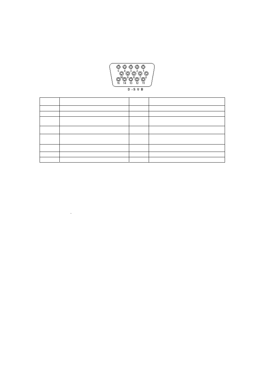
1.4 Connector Pin Assignment
1.4.1 D-sub mini 15pin Connector
Pin No.
Pin Function
Pin No.
Pin Function
1
Red video input
9
NC
2 Green
video
input
10 Ground
3
Blue video input
11
NC
4 NC
12 (SDA)
5 Ground
13
Horizontal synchronization
(Composite sync)
6
Red video ground
14
Vertical
synchronization
7 Green
video
ground
15 (SCL)
8
Blue video ground
1.4.2 DC Connector
DC Power Jack, d=2.0mm
12
Please refer to Chapter 5 for more detail regarind the DC Connector
1.4.3 Audio Connector (Optional)
Phone Jack, d=3.5mm
13
Operating Instructions
Chapter 2
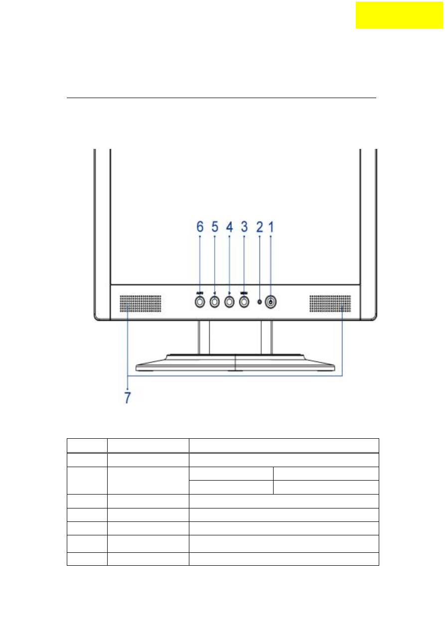
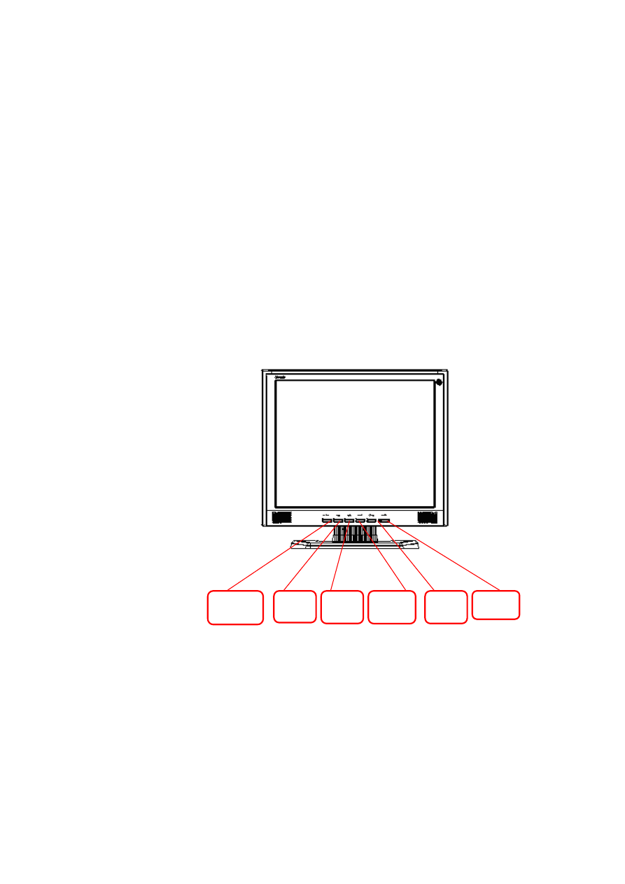
2.1 Function Names
2.1.1
Front
No. Name
Descriptions
1 Power
Switch
Power
On/Off
2
LED Indicator
Green
Normal operation
Orange Power
management
3
MENU
OSD control MENU button
4
>
Right selection/ Volume button (AL1512m)
5
<
Left selection/ Volume button (AL1512m)
6
AUTO
Adjust Clock, Phase, H Position and V Position
automatically
7 Speaker
1.5W
x
2
14
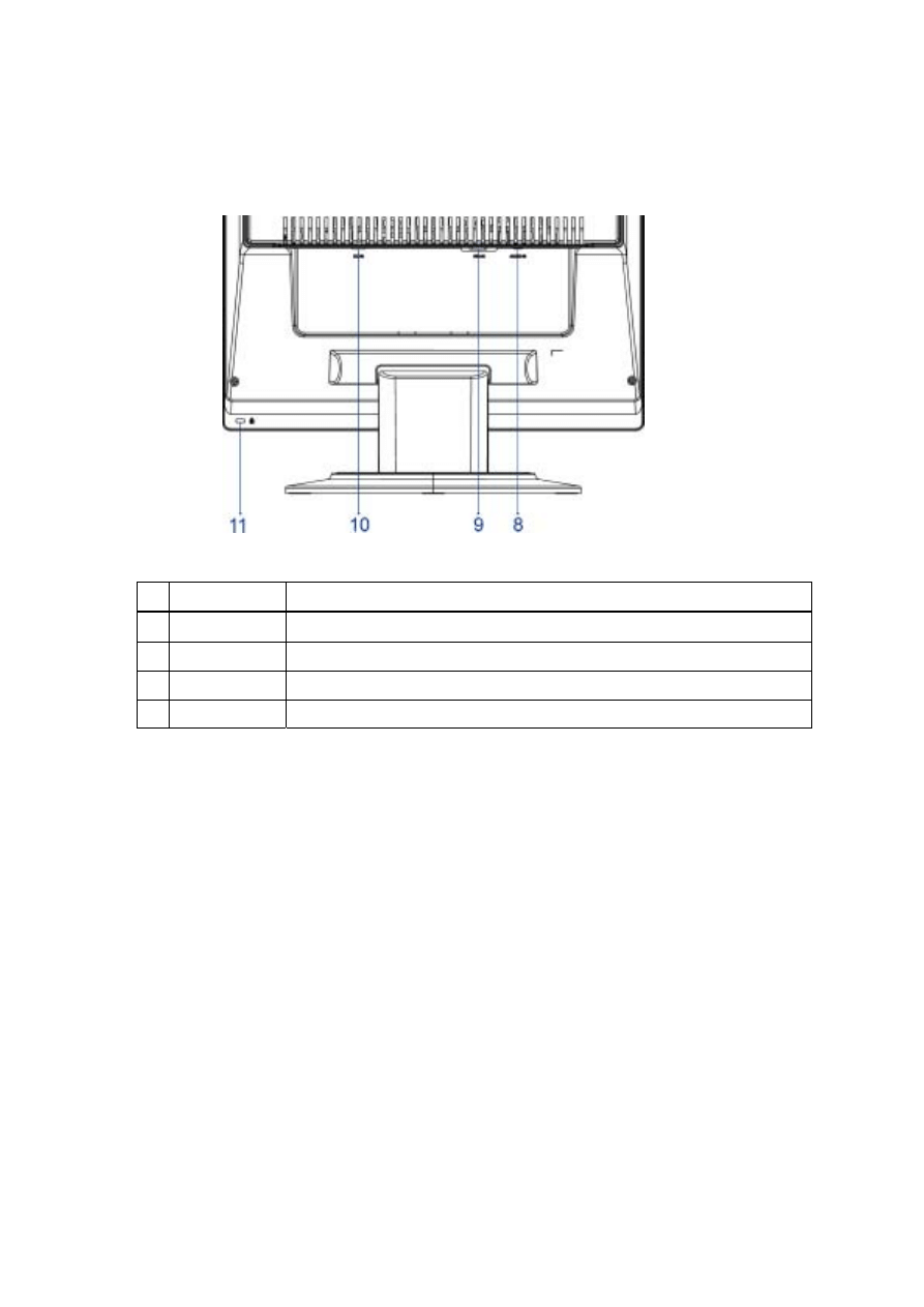
2.1.2
Back
No. Name
Descriptions
8
AUDIO-IN
d=3.5mm stereo mini Jack
9
VGA-IN
D-sub mini 15pin Connector
10
DC-IN
DC Power Jack, d=2.0mm.
11 Lock
hole Kinglock
15
2.2 OSD Menu Description
1. Power : Press this key to control power ON/OFF of the Monitor.
Green: Power is on and normal .
Orange: Power off.
Orange Sleep status in the energy-saving mode.
2. Menu : Press this button to enter OSD. Press it again to exit OSD.
3. > / Plus and < / Minus : Press this button for selection or
adjustment when OSD is shown. Press this button and click < and
> to adjust volume when OSD is not shown (for the model with
speakers only)
4. Auto : Press this button to exit the manual when OSD is shown.
Press this button for the display to optimize the position, phase and
clock pulse automatically when OSD is not shown.
Auto
LED
Menu
<
>
Power
`
16
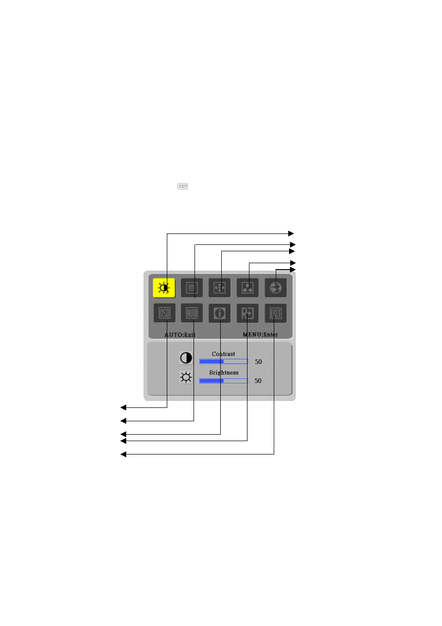
2.3 OSD Operation
Click MENU to display the OSD window as shown in the following
figure.
Click < or > to select the function to be adjusted as shown in the
following figure.
Click the MENU to select the function to be adjusted.
Click < or > to change current settings.
To exit OSD, select “
” to close the OSD window and save changes.
To change other settings repeat steps 2-4. .
Bright/Contract Adjustment
Phase/Clock pulse Adjustment
Horizontal/Vertical Adjustment
Color Temp. Adjustment
Language Selection
OSD Setting
Auto Adjustment
Message
Restore
Exit
17
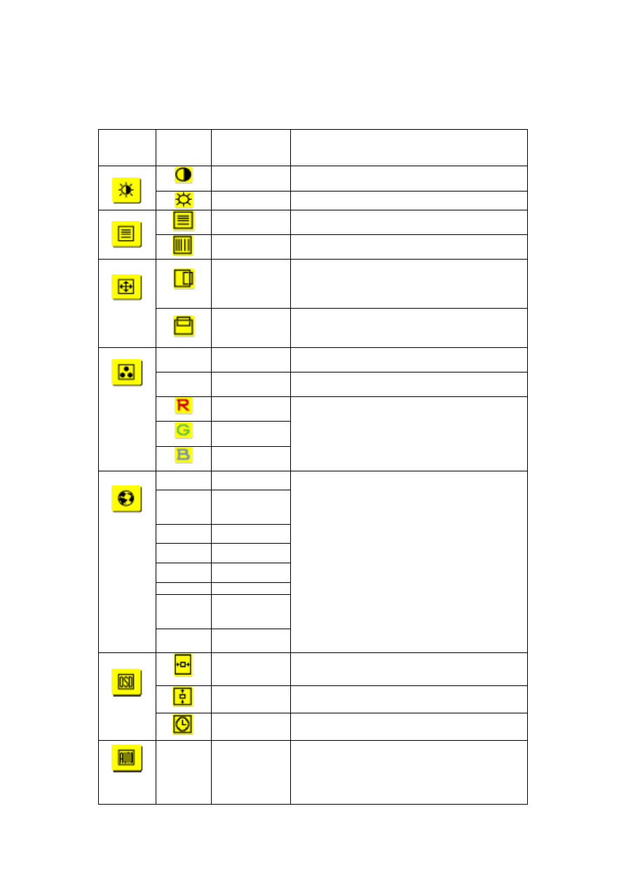
2.4 OSD function definition
Primary
Directory
Symbol
Secondary
Directory
Symbol
Secondary
Directory Items
Description
Contrast
Adjust the contrast between the foreground and
background of an image on the screen
Brightness
Adjust the background brightness of the screen
Phase
Adjust the focus of the image (for analog input
adjustment only)
Clock Pulse
Adjust the clock pulse of the image (for input
adjustment only)
Horizontal
Move the image left and right on the screen (for
input adjustment only)
Vertical
Move the image up and down on the screen (for
input adjustment only)
N/A
Warm Color
Temp.
Set up the color temp. to be warm white color
N/A
Cold Color
Temp.
Set up the color temp. to be cold white color
User
Definition/Red
User
Definition/Green
User
Definition/Blue
Adjust red/green/blue gain
N/A
English
N/A
(Complex
Chinese)
N/A
Deutsch
N/A
Français
N/A
Español
N/A
Italiano
N/A
(Simplified
Chinese)
N/A
(Japanese)
Select the language you want
Horizontal
Move OSD left and right
Vertical
Move OSD up and down
OSD Time
Display
Adjust OSD time display settings
N/A
Auto
Adjustment
Set up horizontal, vertical, sequence and focus
automatically
18

(for analog input
only)
N/A
Message
Display resolution, H/V frequency and the input
port used for current input timing function.
N/A
Restore
Restore to factory settings
N/A
Exit
Close the OSD window and save changes.
2.5 Plug and Play
The product provides the latest VESA plug and play function to
prevent complicated and time-consuming installation procedures. The
plug and play function allows your computer system to identify the
LCD display easily and set up the functions of the LCD display
automatically.
The LCD display transfers the Extended Display Identification Data
(EDID) to your computer system via the Display Data Channel (DDC),
so that your computer can use the self-setting function of the LCD
display.
2.6 Power Saver
The LCD display has a built-in Power Control System (Power Saver).
When the LCD display is not operated during a certain time, the
Power Control System will brings the LCD display into low voltage
status automatically to save power. Move the mouse slightly or press
any key to return to the normal operation.
The Power Saver function can only be operated by the display card of
the computer system. You can set up this function from your computer.
The LCD display is compatible with EPAENERGY STAR NÜTEK
when used with VESA DPMS
To save power and extend the life of the product, turn off the LCD
display power supply when it is not used or when remaining idle for a
long time.
19
Dissassembly and Reassembly
3.1 Disassembly Procedures
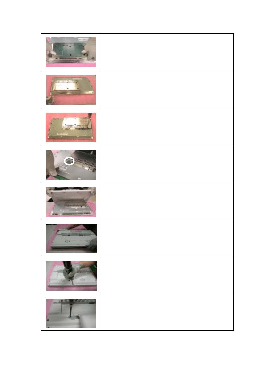
Chapter 3
Picture Description
Push the hooks and stand bottom away
Remove Hinge Cover
Loosen and remove 6 screws to remove Stand Assy
Loose and remove 5 screws.
Separate Bezel hooks to take Bezel and Rear Cover
apart.
Lift up Rear Cover
20
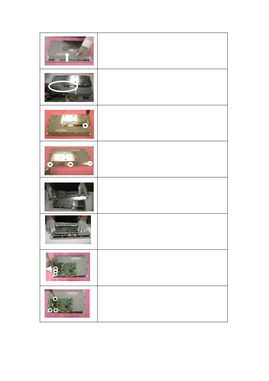
Pull out FFC from connectors at Switch Board and
AD PCBA
Loose and remove 2 Stand-Off screws
Stand-Off Part No : 42A9940007
Loose and remove 1 screw
Loosen & Remove 3 screws
Open & Separate Metal Cover (PCB-X)
Remove the Cover of main board
Remove 3 Backlight wires.
Loose and remove 3 screws
21
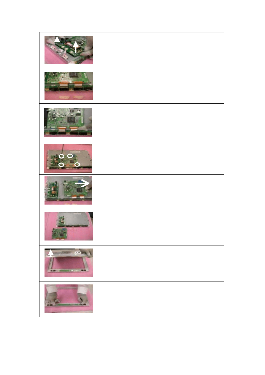
Lift up Inverter slightly, and Separate its head from
the housing at AD PCBA
Remove the taps on X-board FPC.
Pull out the X-Board FPC
Loose and remove 4 screws
Remove AD PCBA
Disassembly PCBA complete.
Lift up LCD module and remove bezel.
Separate both Audio Cable.
22
Loose and remove 2 screws.
Take Function PCBA apart completed
3.2 Reassembly Procedures
Place Function PCBA.
Fasten 2 screws
Insert Audit Cable to connectors .
Bezel assembly complete.
Place LCD module.
23
Place new AD PCBA
Fasten 4 screws
Insert FPC to connector
Shift Inverter with care ; plug its head into the
housing at AD PCBA
Fasten 3 fixed screws.
Insert 3 Backlight wires
Place Metal Cover (AD/Power-PCB)
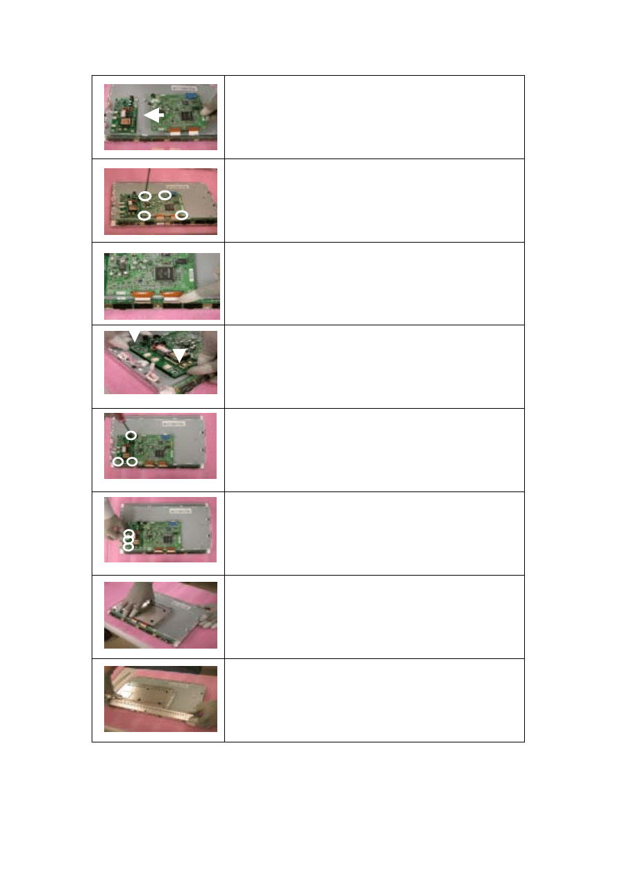
Place Metal Cover (PCB-X)
24
Push the metal Cover (PCB-X) andforward to have
the hook latched.
Fasten 3 screws
Fasten the screw
Fasten 2 Stand-Off screws
Place Rear Cover
Join hooks of Rear Cover
with Bezel
Fasten 5 screws
Place Stand Assy.
Fasten 6 screws
25

Insert Stand Cover
Have the hook latched
26
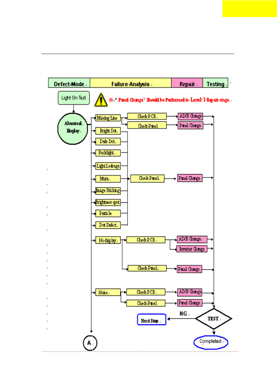
Troubleshooting
Chapter 4
4.1 Abnormal Display Troubleshooting
27
28
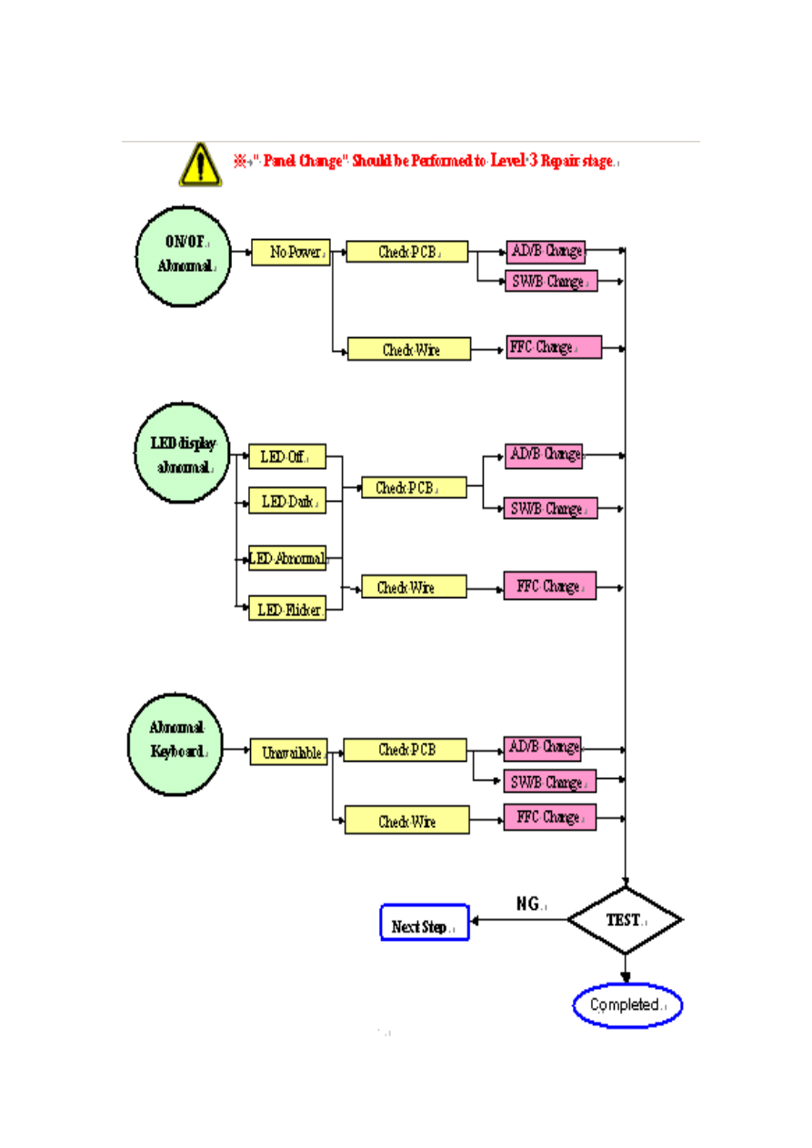
4.2 Abnormal (ON/OFF, LCD display, Keyboard ) Troubleshooting
29
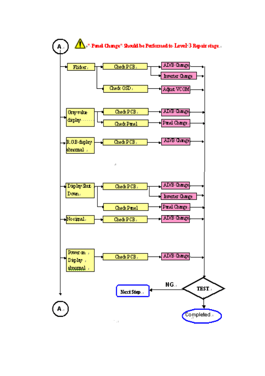
4.3 Abnormal (BIOS, OSD, Other Display ) Troubleshooting
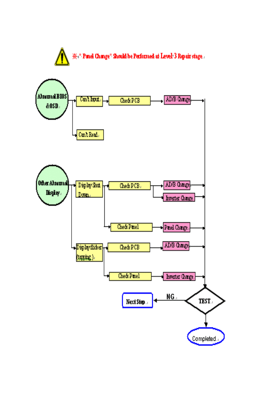
30
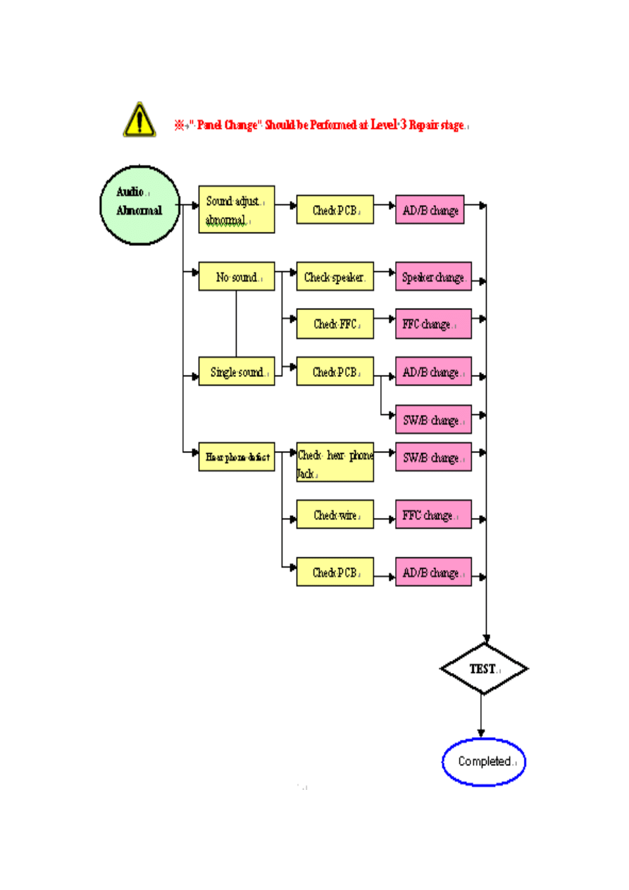
4.4 Audio Abnormal Troubleshooting
31
Connector Information
Chapter 5
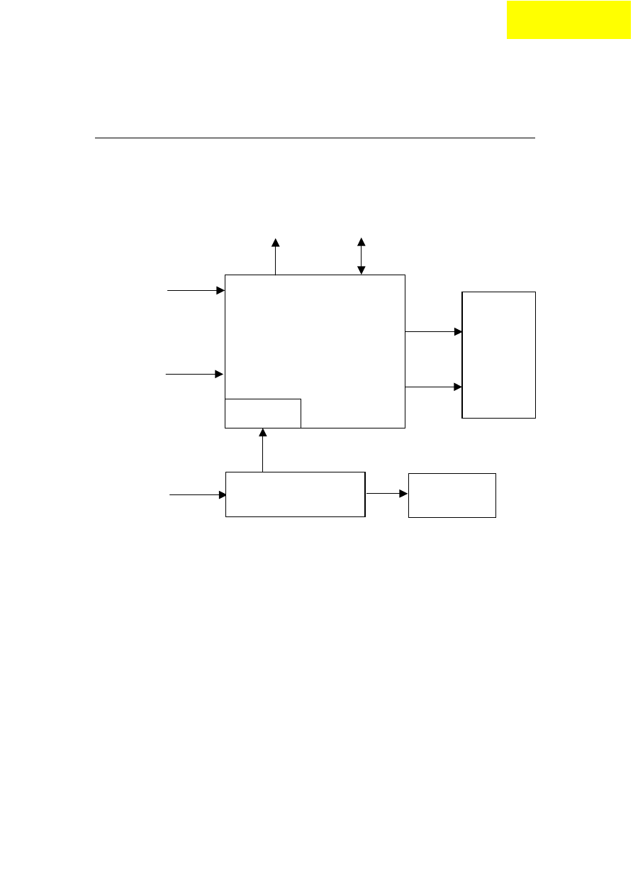
5.1 Function block Diagram
Audio
Speaker
Audio In
Signal
3.3V
D-sub
Analog Video
DC12V
LCD
Backlight
Inverter
Main
DC/D
DC -12V
OSD Key
32
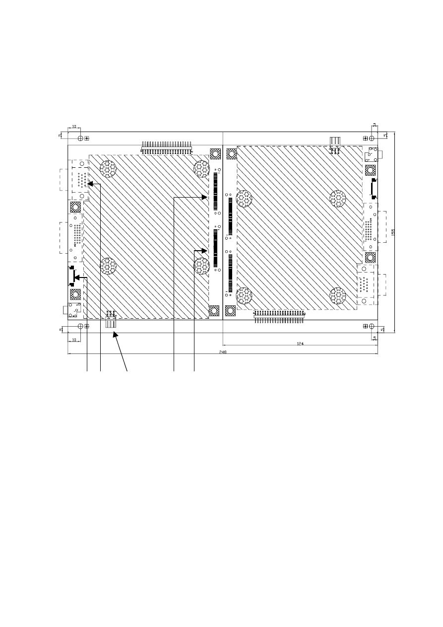
5.2 Connector Location
CN3
CN2
CN4
JP1
CN5
33

5.3 Main Board Pin Assignment Introduction
5.3.1 CN2 Pin assignment
Pin No.
Symbol
Description
1
STV1
SCAN IC START PULSE
2
OE
SCAN DATA OUTPUT ENABLE
3
CKV
SCAN IC CLOCK
4 GND
GROUND
5
STH1
SHIFT START PULSE I/O
6 REV1 DATA
INVERSION
INPUT
7 REV2 DATA
INVERSION
INPUT
8 POL
POLARITH
INVERTING
9 STB
DATA
LATCH
10 GND
GROUND
11
CKH
DATA CLOCK INPUT
12 GND
GROUND
13 GMA1
GAMMA
VOLTAGE
14 GMA2
GAMMA
VOLTAGE
15 GMA3
GAMMA
VOLTAGE
16 GMA4
GAMMA
VOLTAGE
17 GMA5
GAMMA
VOLTAGE
18 GMA6
GAMMA
VOLTAGE
19 GMA7
GAMMA
VOLTAGE
20 GMA8
GAMMA
VOLTAGE
21 GMA9
GAMMA
VOLTAGE
22 GMA10
GAMMA
VOLTAGE
23 GND
GROUND
24
VCOM
PANEL COMMOM VOLTAGE
25
VCOM
PANEL COMMOM VOLTAGE
26
VCOM
PANEL COMMOM VOLTAGE
27
VCOM
PANEL COMMOM VOLTAGE
28
VCOM
PANEL COMMOM VOLTAGE
29
VSA
DRIVER SUPPLY VOLTAGE
30
VSA
DRIVER SUPPLY VOLTAGE
31
VSA
DRIVER SUPPLY VOLTAGE
32
VSA
DRIVER SUPPLY VOLTAGE
33
VSA
DRIVER SUPPLY VOLTAGE
34
34
VSD DATA
IC
VOLTAGE
35 VSD
DATA
IC
VOLTAGE
36 VSD
DATA
IC
VOLTAGE
37
VDDY
DRIVER SUPPLY VOLTAGE
38
VDDY
DRIVER SUPPLY VOLTAGE
39
DRESTOUT
OUTPUT ALL-ON CONTROL
40
PANEL VGL
PANEL DRIVING VOLTAGE
41
PANEL VGL
PANEL DRIVING VOLTAGE
42 GND
GROUND
43
PANEL VGH
PANEL DRIVING VOLTAGE
44
PANEL VGH
PANEL DRIVING VOLTAGE
45 GND
GROUND
5.3.2 CN3 Pin assignment
Pin No.
Symbol
Description
1
GND GROUND
2
GND GROUND
3
ER0
EVEN PATH RED DATA BIT
4
ER1
EVEN PATH RED DATA BIT
5
ER2
EVEN PATH RED DATA BIT
6
ER3
EVEN PATH RED DATA BIT
7
ER4
EVEN PATH RED DATA BIT
8
ER5
EVEN PATH RED DATA BIT
9
GND GROUND
10
EG0
EVEN PATH GREEN DATA BIT
11
EG1
EVEN PATH GREEN DATA BIT
12
EG2
EVEN PATH GREEN DATA BIT
13
EG3
EVEN PATH GREEN DATA BIT
14
EG4
EVEN PATH GREEN DATA BIT
15
EG5
EVEN PATH GREEN DATA BIT
16
GND GROUND
17
EB0
EVEN PATH BLUE DATA BIT
18
EB1
EVEN PATH BLUE DATA BIT
19
EB2
EVEN PATH BLUE DATA BIT
20
EB3
EVEN PATH BLUE DATA BIT
21
EB4
EVEN PATH BLUE DATA BIT
22
EB5
EVEN PATH BLUE DATA BIT
23
GND GROUND
35
24
OR0
ODD PATH RED DATA BIT
25
OR1
ODD PATH RED DATA BIT
26
OR2
ODD PATH RED DATA BIT
27
OR3
ODD PATH RED DATA BIT
28
OR4
ODD PATH RED DATA BIT
29
OR5
ODD PATH RED DATA BIT
30
GND GROUND
31
OG0
ODD PATH GREEN DATA BIT
32
OG1
ODD PATH GREEN DATA BIT
33
OG2
ODD PATH GREEN DATA BIT
34
OG3
ODD PATH GREEN DATA BIT
35
OG4
ODD PATH GREEN DATA BIT
36
OG5
ODD PATH GREEN DATA BIT
37
GND GROUND
38
OB0
ODD PATH BLUE DATA BIT
39
OB1
ODD PATH BLUE DATA BIT
40
OB2
ODD PATH BLUE DATA BIT
41
OB3
ODD PATH BLUE DATA BIT
42
OB4
ODD PATH BLUE DATA BIT
43
OB5
ODD PATH BLUE DATA BIT
44
GND GROUND
45
GND GROUND
5.3.3 CN4 Pin assignment
Pin No.
Symbol
Description
1 INV_ADJ
Brightness
Adjustment
2 INV_ON/OFF
Inverter
enable
3 GND
Ground
4 GND
Ground
5 VIN_12V
Input
source
6 VIN_12V
Input
source
36

5.3.4 CN5 Pin assignment
Pin No.
Symbol
Description
1 NC
2 AUTO_ADJ
AUTO
ADJUSTMENT
3 NC
4 EXIT
EXIT
KEY
5 MENU
MENU
KEY
6 GND
GROUND
7 UP
UP
KEY
8
LED OR
ORANGE LED
9
LED GR
GREEN LED
10 POWER_KEY
POWER
KEY
11 NC
12 HP_Detector
HEADPHONE
DETECT
13 DOWN
DOWN
KEY
14 NC
15 AUDIO/R-
AUDIO
OUTPUT
16 AUDIO/R+
AUDIO
OUTPUT
17 AUDIO/L-
AUDIO
OUTPUT
18 AUDIO/L+
AUDIO
OUTPUT
37
5.3.5 JP1 Pin assignment
Pin No.
Symbol
Description
1 GRAI
RED
INPUT
2 GGAI
GREEN
INPUT
3 GBAI
BLUE
INPUT
4 NC
5 GND
GROUND
6
RGND
RED INPUT GROUND
7
GGND
GREEN INPUT GROUND
8
BGND
BLUE INPUT GROUND
9 VGA_5V
VGA
INPUT
5V
10 GND_ANA
GROUND
11 NC
12 DSUB-SDA
I2C
13 G_HSYNC
H-SYNC
14 G_VSYNC
V-SYNC
15 DSUB_SCL
I2C
38
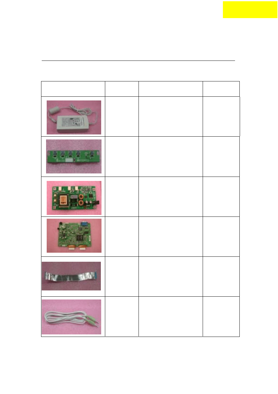
FRU (Field Replaceable Unit) List
Part List
Picture Partname Description
Vendor
Part No.
Adapter
Adaptor(AC/DC),40W,12
V,3.33A,UP04081120-
01W
2719040122
FUNCTION
BUTTON
BOARD
PCBA ,Rigid,201-0M
35A15K0218
INVERTER
BOARD
DC/AC
INVERTER,TWS-444-
936, TYP.2400V/5MA
2714000001
Main Board PCBA ,Rigid,203-03
35A15S0236
CABLES
FFC
AD_OSD_GROUNDING,
TennRich,121.5*9.5mm
3241500004
AUDIO
CABLE
28AWG,180 cm
32F2818001
Chapter 6
39
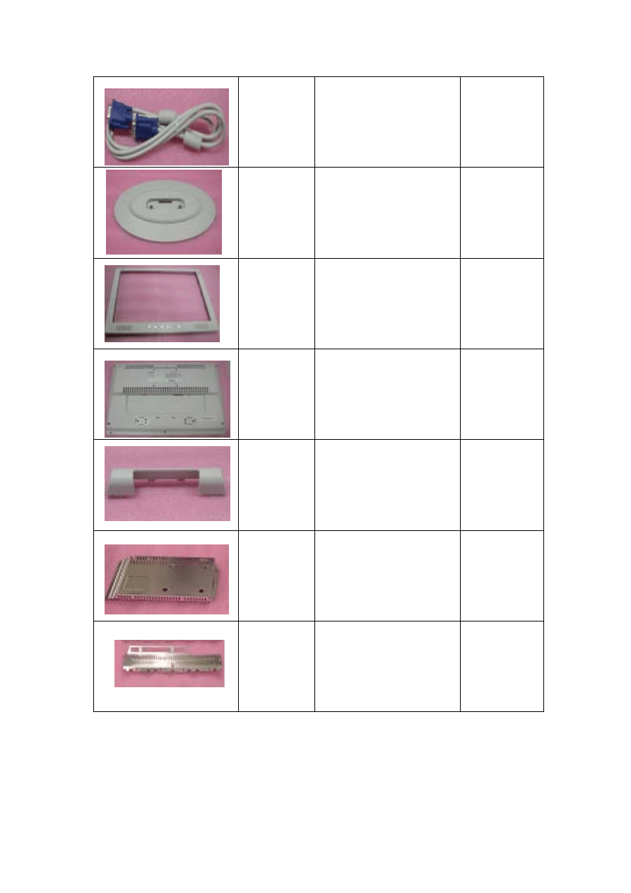
MONITOR
CABLE
427C,30AWG,180cm 32F3018001
STAND
BASE
Seat Assy,
40A15929D3
LCD
FRONT
BEZEL
Bezel Assy
40A1529947
LCD
BACK
COVER
Rear Assy
40A15929C4
Hinge Cover Cover Hinge
40A15929D5
MAINBOAR
D COVER
Cover_pcb_ad, D-Sub
Only
41A1599115
LCD
BRACKET
METAL COVER PCB-X, 41A1599116
40
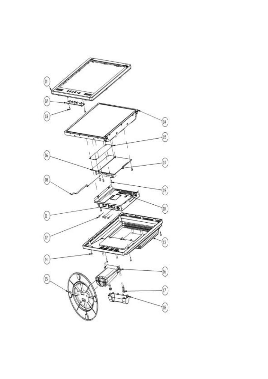
Explosion Diagram
1.BEZEL_W/_SPEAKER_ASSY
2.OSD PCBA
3.SCREW
4.PANEL ASSY
5.PET_FILM_METAL_FRAM_R
EAR
6.INVERTER
7.SMART PCBA
8.FFC AD_OSD
9.SCREW
10.PET ISOLUTION FILM
11.METAL COVER SMART
12.STAND-OFF
13.REAR_ASSY
14.SCREW
15.SEAT_ASSY
16.STAND_ASSY
17.SCREW
18.STAND HINGE_COVER
41
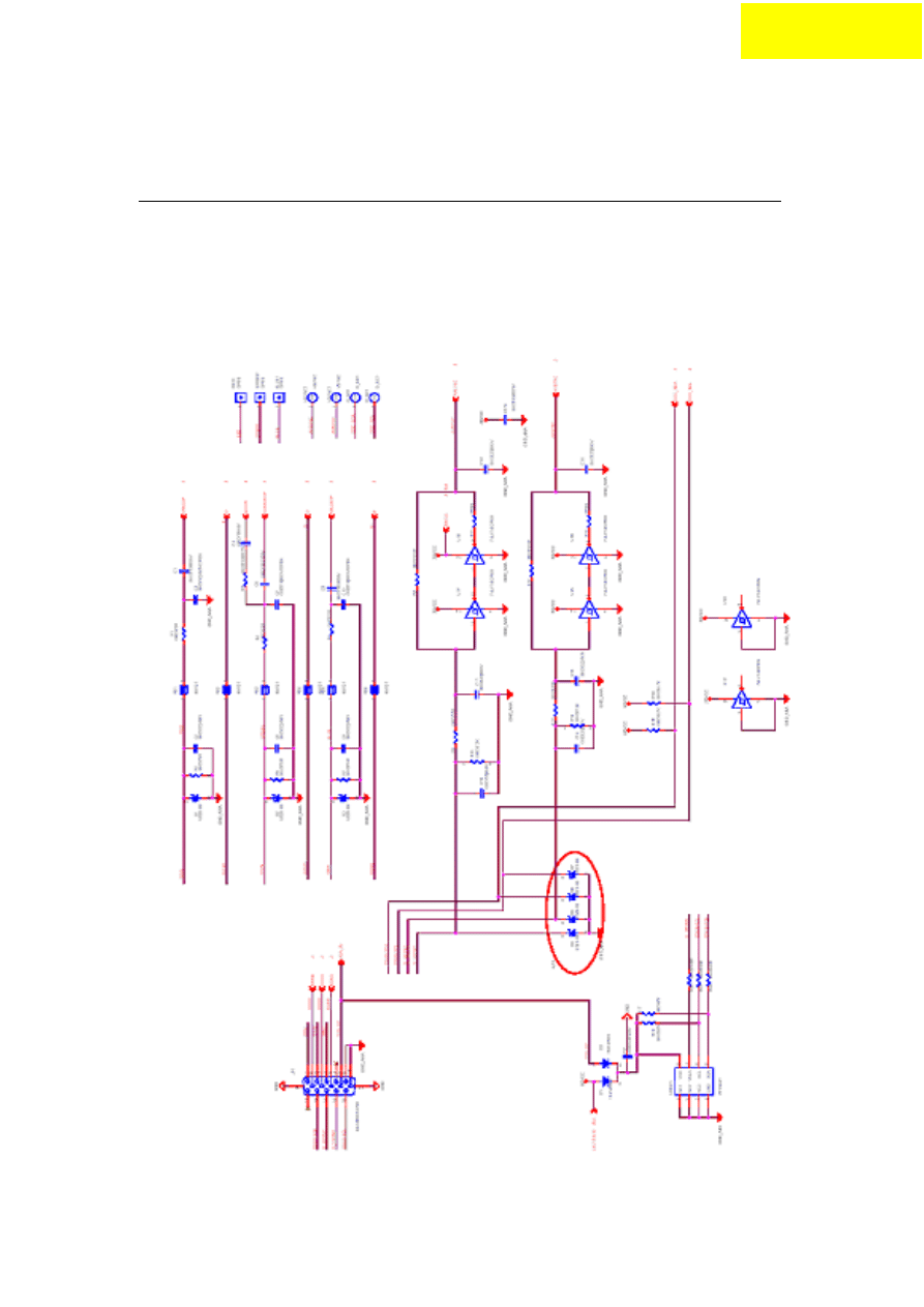
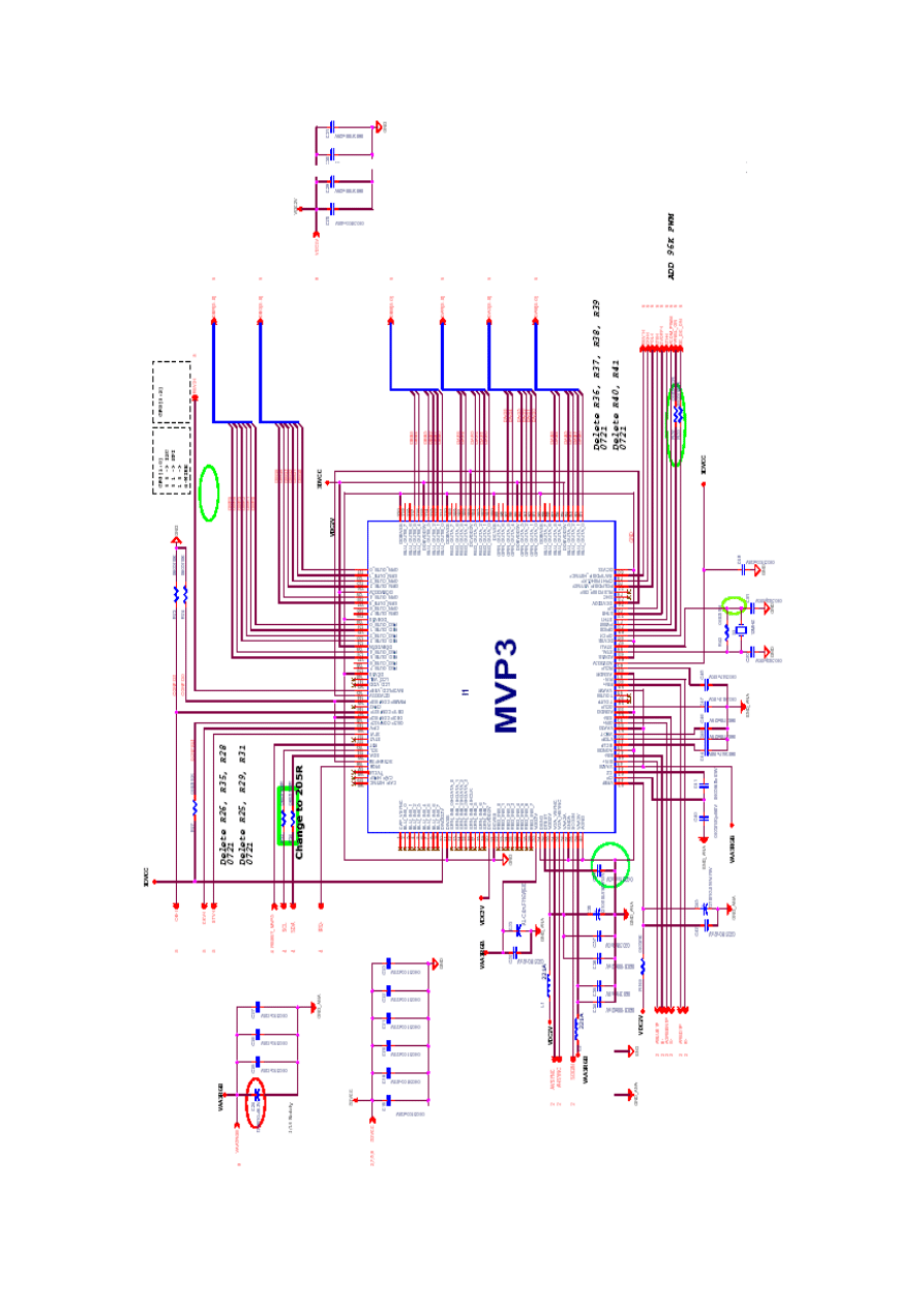
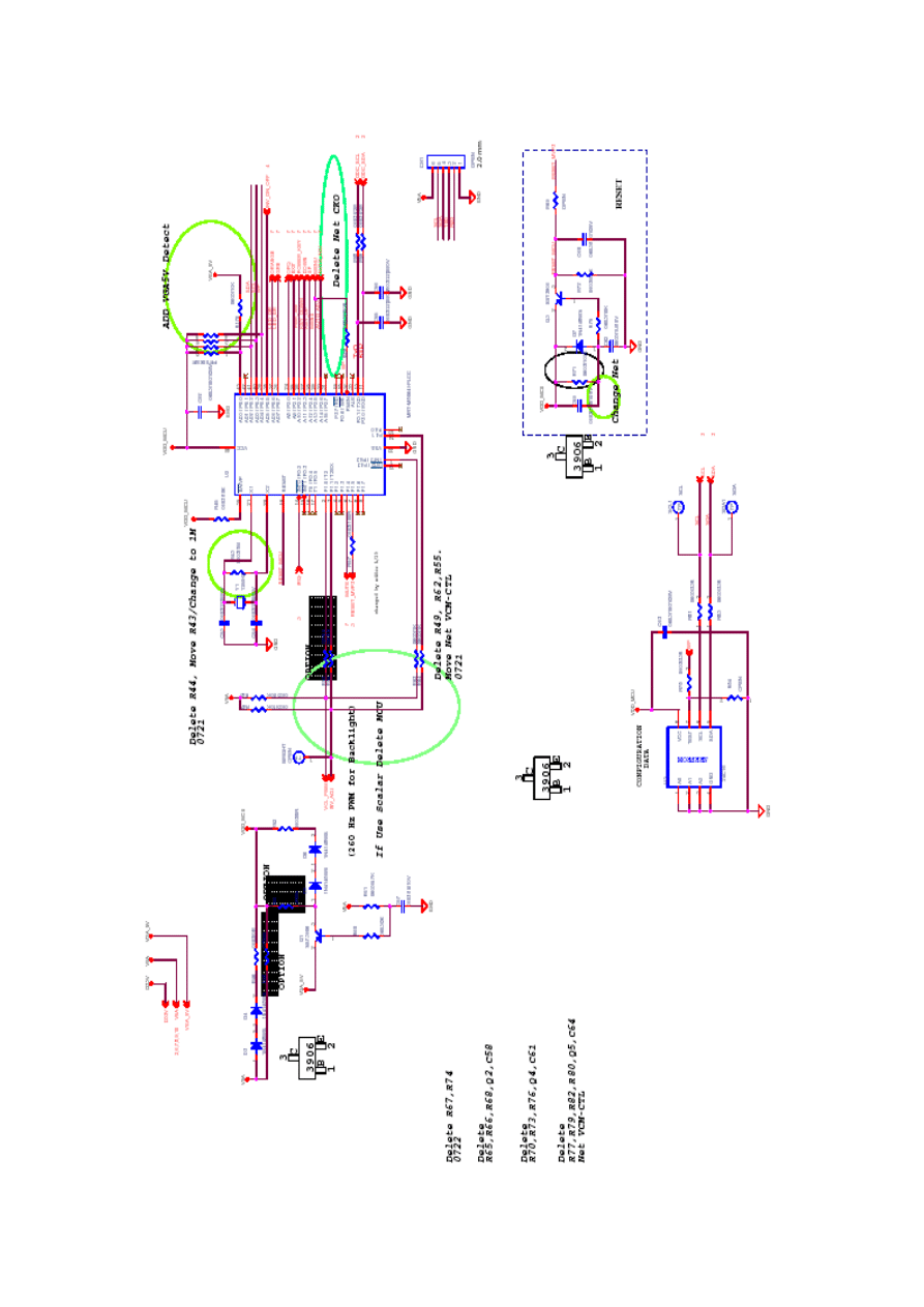
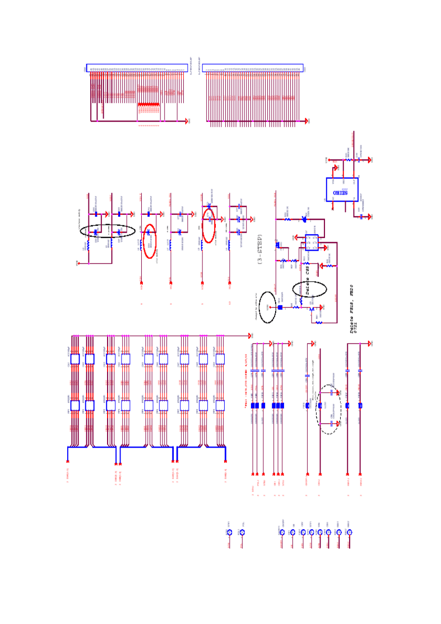
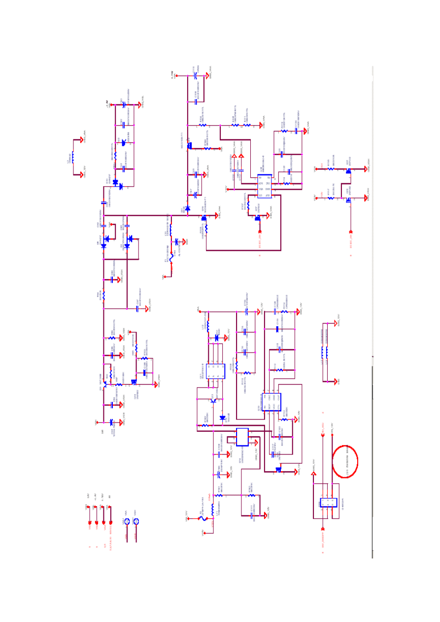
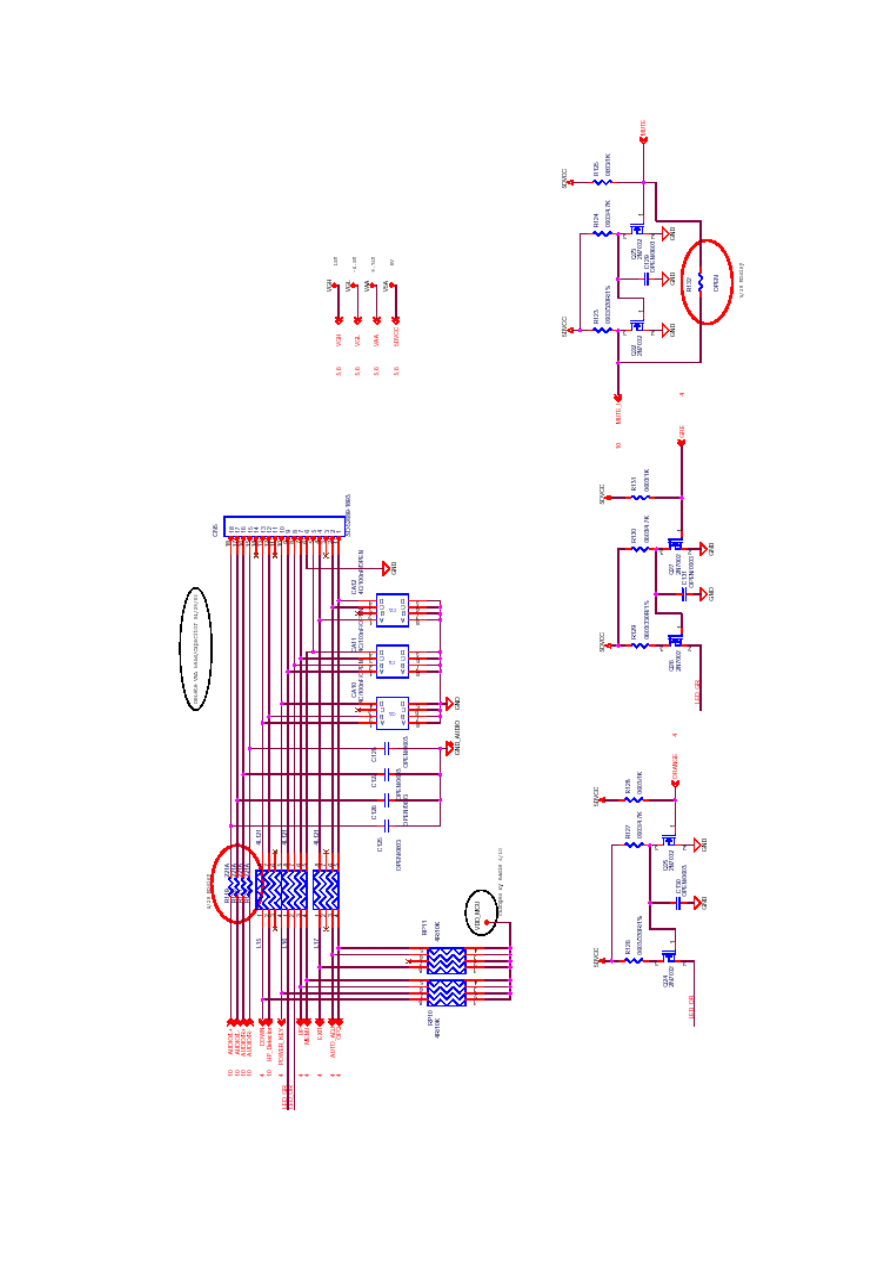
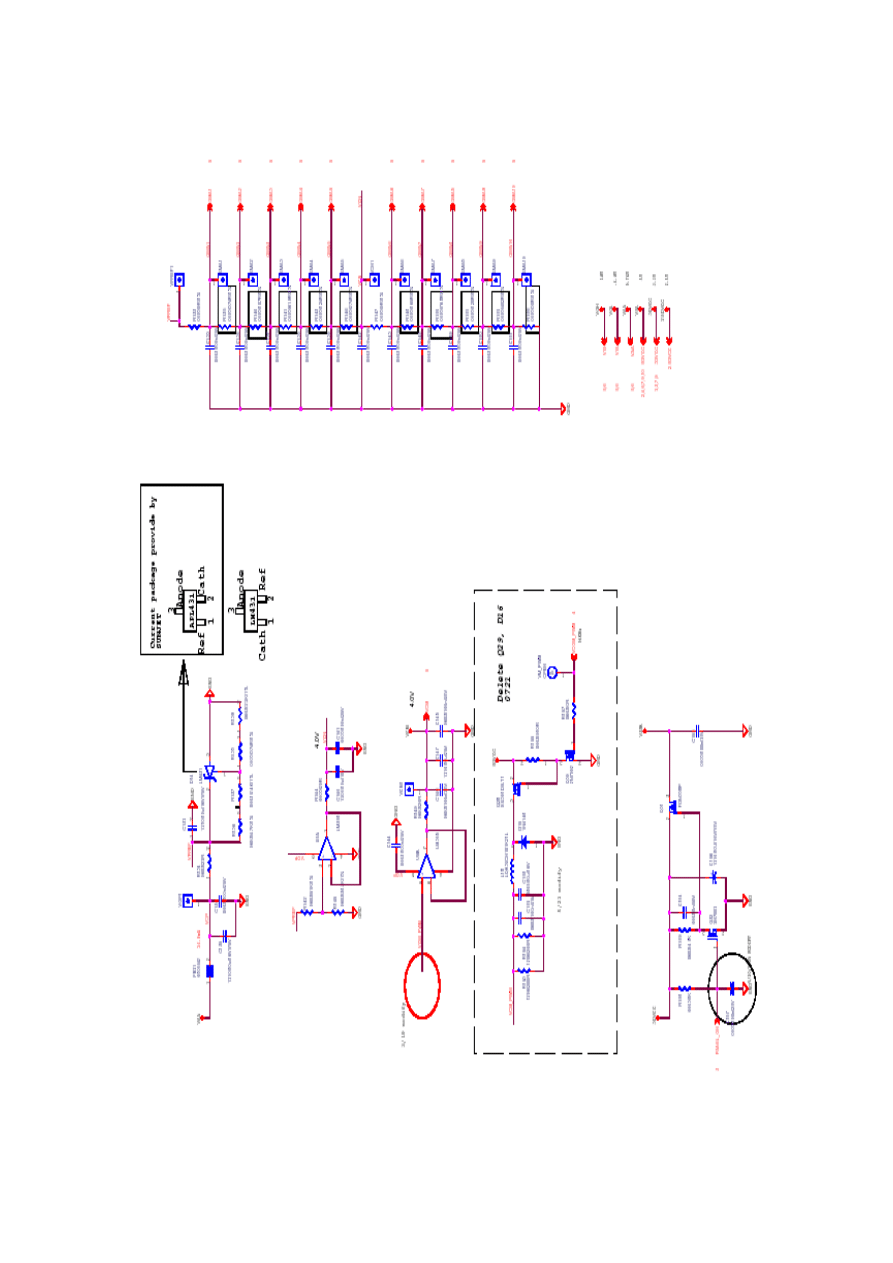
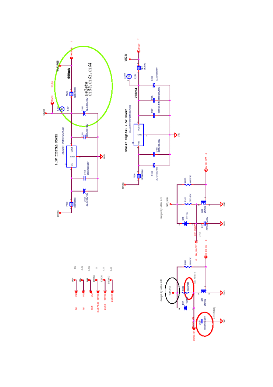
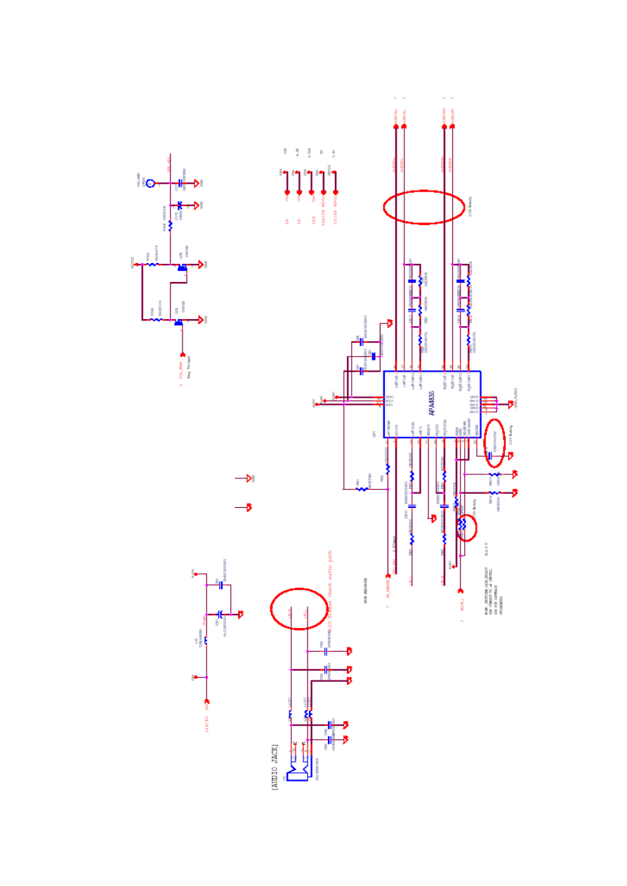
Schematic Diagram
Chapter 7
Main Board
42
43
44
45
46
47
48
49
50
Document Outline
- AL1512
- Copyright
- Disclaimer
- Conventions
- Preface
- Warning
- Precautions
- Table of Contents
- CH1_Monitor Features
- CH2_Operating Instructions
- CH3_Disassembly and Reassembly
- CH4_ Troubleshooting
- CH5_Connector Information
- CH6_FRU
- CH7_Schematic Diagram
Wyszukiwarka
Podobne podstrony:
Acer TFT LCD Color Monitor AL1713 Parts and Service
Service Manual Sony TFT LCD Color Monitor CPD L133 Schematic
MX 100 PARTS & SERVICE MANUAL
Instrukcja obsługi KAMERY SAMOCHODOWEJ TFT LCD 2,5
XC 50 PARTS & SERVICE MANUAL
Dell LCD Monitor 1503FP Service Manual
@What is TFT LCD TV and LCD Monitor Panel 2
ACER E390 Notebook Tft
Manual Acer TravelMate 2430 US EN
A10VO Series 31 Size 28 Service Parts list
acer
Proview RA783 LCD Service Manual
Proview PZ456 LCD Service Manual
130 cc Pump Service Parts
Proview SH770I LCD Service Manual
Proview AY765 LCD Service Maunal
Acer gatunki introdukowane
więcej podobnych podstron