
Nucleation layer evolution in metal-organic chemical vapor deposition
grown GaN
X. H. Wu, D. Kapolnek, E. J. Tarsa, and B. Heying
Materials Department, College of Engineering, University of California, Santa Barbara, California 93106
S. Keller, B. P. Keller, and U. K. Mishra
Electrical and Computer Engineering Department, College of Engineering, University of California,
Santa Barbara, California 93106
S. P. DenBaars
Materials Department and Electrical and Computer Engineering Department, College of Engineering,
University of California, Santa Barbara, California 93106
J. S. Speck
a)
Materials Department, College of Engineering, University of California, Santa Barbara, California 93106
~Received 25 September 1995; accepted for publication 8 January 1996!
The structure and morphology of low growth temperature GaN nucleation layers have been studied
using atomic force microscopy
~AFM!, reflection high energy electron diffraction ~RHEED!, and
transmission electron microscopy
~TEM!. The nucleation layers were grown at 600 °C by
atmospheric pressure metalorganic chemical vapor deposition
~MOCVD! on c-plane sapphire. The
layers consist of predominantly cubic GaN
~c-GaN! with a high density of stacking faults and twins
parallel to the film/substrate interface. The average grain size increases with increasing layer
thickness and during the transition from low temperature
~600 °C! to the high temperatures
~1080 °C! necessary for the growth of device quality GaN. Upon heating to 1080 °C the nucleation
layer partially converts to hexagonal GaN
~h-GaN! while retaining a high stacking fault density. The
mixed cubic-hexagonal character of the nucleation layer region is sustained after subsequent
high-temperature GaN growth. © 1996 American Institute of Physics.
@S0003-6951~96!01710-8#
The high interfacial energy associated with GaN thin
films on sapphire substrates leads to three-dimensional island
growth of the GaN. As a result, a two-step metalorganic
chemical vapor deposition
~MOCVD! growth process has
been developed to promote two-dimensional GaN growth on
sapphire.
1,2
This process involves the growth of GaN or AlN
nucleation layers at low temperatures, followed by the
growth of the device quality GaN film at high temperature.
High nucleation densities are more readily achieved at low
temperatures, where the supersaturation of the growth spe-
cies above the substrate is high and adatoms have low sur-
face mobilities. In contrast, stabilization of the hexagonal
phase of GaN
~h-GaN! is achieved at high temperatures
where surface mobilities are sufficient to facilitate step-flow
growth.
3
The
;14% lattice mismatch between h-GaN ~a53.180
Å, c
55.166 Å! and basal plane sapphire ~
a
-Al
2
O
3
, a
54.755 Å, a/A352.748 Å, c512.991 Å! leads to unavoid-
ably high misfit dislocation densities. As a consequence, high
threading dislocations densities (
.10
10
cm
22
) are often ob-
served throughout GaN films grown on sapphire.
4 – 6
Re-
cently, we have been able to successfully grow films with
threading dislocation densities of
;7310
8
cm
22
by opti-
mizing the nucleation layer growth conditions.
3
Previous
studies have demonstrated that nucleation layer growth con-
ditions strongly affect the electrical and optical properties of
GaN device layers.
2,7,8
In general, the structure of the nucle-
ation layer is believed to evolve as the temperature is in-
creased prior to bulk film growth.
7–9
However, detailed char-
acterization of the nucleation layer microstructure has yet to
be reported. Since the nucleation layer serves as the crystal-
lographic and morphological template for subsequent GaN
deposition, the structure of this layer must be understood for
the ultimate optimization of GaN device structures on sap-
phire. In this letter, we present the characterization of the
morphology and crystallinity of as-grown GaN nucleation
layers and the microstructural evolution of these layers as
they are heated to typical GaN growth temperatures.
The GaN nucleation layers were grown on c-plane sap-
phire using a horizontal flow atmospheric pressure metalor-
ganic chemical vapor deposition
~MOCVD! reactor ~Thomas
Swan Co., Ltd.
!. The substrates were first cleaned with sol-
vents and subjected to an in situ pretreatment in flowing H
2
at 1050 °C. The nucleation layers were grown at 600 °C us-
ing trimethylgallium
~TMGa! and ammonia (NH
3
). Some
nucleation layers were quenched to room temperature imme-
diately following growth, while others were heated to
1080 °C and held for several seconds prior to quenching.
This was done to investigate the evolution of the nucleation
layer during different stages of the standard GaN film growth
process. The nucleation layers were characterized using
atomic force microscopy
~AFM! in tapping mode, reflection
high energy electron diffraction
~RHEED!, and cross-
sectional transmission electron microscopy
~TEM!. RHEED
studies were performed using 7 keV electrons in a separate
molecular beam epitaxy chamber.
The initial stages of GaN nucleation on sapphire were
first examined using AFM. Figure 1 shows AFM micro-
graphs of as-grown nucleation layers of 2 nm
@Fig. 1~a!# and
a
!
Electronic mail: speck@surface.ucsb.edu
1371
Appl. Phys. Lett. 68 (10), 4 March 1996¬0003-6951/96/68(10)/1371/3/$10.00¬© 1996 American Institute of Physics
Copyright ©2001. All Rights Reserved.
20 nm
@Fig. 1~b!# nominal thickness. The average grain size
increases from 25 to 33 nm and the rms roughness increases
from 3.11 to 6.18 nm as the nominal thickness increased
from 2 to 20 nm. The morphology of the films after heating
to 1080 °C
@Fig. 1~c!# will be discussed below.
The as-grown 20 nm thick nucleation layer surfaces pro-
duced RHEED patterns corresponding primarily to
@111# ori-
ented cubic GaN
~c-GaN!, with 180° rotational twinning
about the surface normal, as evident in the
@11¯0#
c
azimuth
RHEED pattern in Fig. 2
~a! ~calculated diffraction patterns
with one c-GaN variant are also shown in Fig. 2
!. The
RHEED pattern was spotty in the
@21¯ 1¯#
c
azimuth
~the sub-
script c refers to cubic indexing and the subscript h refers to
hexagonal
!, as shown in Fig. 2~b!, thus indicating that the
surface is three dimensional. In contrast, the RHEED pattern
observed along the
@11¯0#
c
azimuth was somewhat streaky,
suggesting a smooth surface. However, cross-section TEM
diffraction showed that the streaking observed along
@11¯0#
c
is not associated with surface morphology but rather with a
high density of stacking faults and twins in the close-packed
~111! c-GaN planes parallel to the film/substrate interface.
Chevroning was evident in
@11¯0#
c
RHEED patterns but not
in
@21¯ 1¯#
c
RHEED patterns. Chevroning is associated with
facet formation and demonstrates that the facet planes lie in a
@11¯0#
c
zone.
Cross-section TEM analysis confirmed the highly faulted
but predominantly cubic character of the 20 nm thick nucle-
ation layers and further showed the highly faceted grain mor-
phology
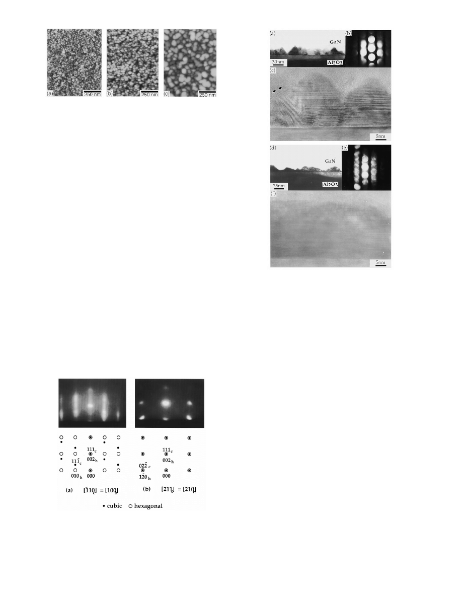
~Fig. 3!. The selected area diffraction pattern shown
in Fig. 3
~b! corresponds to a mixture of c-GaN and h-GaN
with
the
orientation
relationship
@111#
ci
@001#
h
,¬and
@11¯0#
ci
@100#
h
. The regions of pure c-GaN or h-GaN were
composed of only a few close-packed layers, as shown in
both the bright field image of Fig. 3
~a! and the high resolu-
tion image in Fig. 3
~c!. The qualitative difference in intensi-
ties between the unique cubic and hexagonal reflections in
the
@11¯0#
c
zone axis diffraction patterns indicates that this
layer is predominantly c-GaN. This may also be confirmed
by examination of the relative fraction of c-GaN in the high
resolution image
@Fig. 3~c!#. The cubic and hexagonal re-
gions can be easily distinguished in cross-section high reso-
lution images recorded down a
@11¯0#
c
zone axis since the
cubic regions show
$
111
%
c
cross fringes that are inclined
FIG. 1. Tapping mode AFM images of GaN nucleation layers:
~a! as-grown
layer with nominal 2 nm thickness,
~b! as-grown layer with nominal 20 nm
thickness,
~c! nominal 20 nm thick layer after heating to 1080 °C.
FIG. 2. RHEED patterns from as-grown nominally 20 nm thick nucleation
layers
~experimental patterns top, schematic patterns bottom!. ~a! @11¯0#
c
5@100#
h
azimuth
~zone axis!. In this orientation, stacking disorder between
cubic and hexagonal regions leads to streaking.
~b! @21¯ 1¯#
c
5@210#
h
azi-
muth
~zone axis!. In this orientation, cubic and hexagonal stacking se-
quences cannot be distinguished and thus no stacking disorder streaks are
observed.
FIG. 3. Cross-section TEM diffraction and imaging on as-grown nucleation
layers
@~a!, ~b!, and ~c!# and on nucleation layers after high-temperature
exposure
@~d!, ~e!, and ~f!#. The images and diffraction patterns were re-
corded either near or down a
@11¯0#
c
zone axis.
~a! Selected area diffraction
pattern corresponding to predominantly c-GaN.
~b! Bright field image. A
high density faulting density is clearly observed in the GaN grains. Faceting
is also clearly observed.
~c! High resolution image recorded down a
@11¯0#
c
zone axis showing stacking disorder in the grains.
~d! Selected area
diffraction pattern. The diffraction pattern corresponds to mixed c-GaN/h-
GaN.
~e! Bright field image. A high faulting density is clearly observed in
the GaN grains. The grains appear more rounded than the as-grown nucle-
ation layer.
~f! High resolution image showing stacking disorder in the
grains. The outer shell of the grains is predominantly h-GaN.
1372¬Appl. Phys. Lett., Vol. 68, No. 10, 4 March 1996¬Wu
et al.
Copyright ©2001. All Rights Reserved.

70.5° to the film/substrate interface, whereas the hexagonal
regions show vertical (010)
h
fringes.
Although the primary orientation between c-GaN and
h-GaN is
@111#
ci
@001#
h
, and
@11¯0#
ci
@100#
h
, the cubic
phase also displays 180° rotational twinning about
@111#
c
~i.e., @1¯10#
ci
@100#
h
). Since, the reciprocal lattice points for
c-GaN and h-GaN are coincident for a
@21¯ 1¯#
c
5@210#
h
zone
axis, as shown in the schematic diffraction pattern in Fig.
2
~b!, it is not possible to distinguish between cubic or hex-
agonal stacking or resolve stacking disorder in this orienta-
tion. The spotty RHEED patterns recorded along
@21¯ 1¯#
c
5@210#
h
therefore, correctly convey the rough nature of the
GaN surface. In contrast, the reciprocal lattice points for
c-GaN and h-GaN do not coincide in the
@11¯0#
c
5@100#
h
zone axis, as shown in Fig. 2
~a!. Correspondingly, the
@11¯0#
c
5@100#
h
zone axis is sensitive to stacking sequence
and stacking disorder. The streaks observed in RHEED pat-
terns
@11¯0#
c
5@100#
h
therefore originate from stacking dis-
order and not surface morphology.
The morphology of the grains seen in cross-section TEM
is consistent with a
~111! contact plane at the film/substrate
interface and a well-defined facet angle of
;55° with respect
to the substrate. This angle is very close to the angle between
(111)
c
and (100)
c
planes. However, the grains are not proper
single crystals because of their mixed cubic-hexagonal na-
ture and high density of twins. Thus, a proper crystallo-
graphic assignment to the inclined facets is neither possible
nor appropriate. The faceted morphology of the as-grown
nucleation layer was also observed in plan-view TEM. In this
case, both triangular and hexagonal islands were seen in pro-
jection. The island edges were all oriented along one of three
^
110
&
c
direction
~separated by 120°!. For the triangular is-
lands, two orientations were observed corresponding to the
180° twin orientations of c-GaN. The as-grown nucleation
layers displayed a
;1° to 3° in-plane mosaic spread as mea-
sured from selected area electron diffraction patterns.
In addition to planar faulting parallel to the film/
substrate interface, cubic twins were also observed on in-
clined (111
¯)
c
planes, as shown by high resolution TEM
@Fig.
3
~c!#. This result is not surprising as (111)
c
and (111
¯)
c
are
both proper close-packed planes in the cubic phase.
The morphological evolution of a 20 nm thick nucleation
layer heated to 1080 °C is illustrated in the AFM images of
Figs. 1
~b! and 1~c!. During this heating step, the grains un-
derwent substantial growth, resulting in an increase of the
average grain size from 33 to 77 nm. Furthermore, the rms
surface roughness increased from 6.18 to 9.35 nm after heat-
ing. RHEED studies of the nucleation layer have shown that
the surface becomes predominantly h-GaN after exposure to
1080 °C. Cross-section TEM diffraction patterns and micro-
graphs of the nucleation layer after the high-temperature
heating step are shown in Fig. 3. The coalescence of grains at
high temperature is evident in the TEM micrograph shown in
Fig. 3
~d!. Although the structure is still extensively faulted,
selected area electron diffraction
@Fig. 3~e!# shows that the
grains are composed of nearly equal proportions of c-GaN
and h-GaN. Both scattering contrast and high resolution im-
ages
@Fig. 3~f!#, confirm that the grains have lost their dis-
tinct facets and now appear somewhat rounded. However,
the mosaic in the grains determined in plan-view TEM main-
tains a range of
;1° to 3°. The conversion from c-GaN to
h-GaN is predominant near the free surfaces of the grains as
shown in Fig. 3
~f!. Finally, the inclined twins in the cubic
regions were not observed after the high-temperature step.
These results demonstrate that the GaN nucleation layer
is fully crystalline and epitaxial upon growth. Polytypism in
GaN thin films has been previously reported. However, the
predominantly cubic nature of the as-grown nucleation layer
has not been reported. While GaN growth at high tempera-
tures results in a homogeneous h-GaN film, these results sug-
gest that the low-temperature epitaxy is more complicated.
Currently, we can only speculate on the physical basis for the
formation of c-GaN at low temperatures. It would appear that
the formation of the cubic phase may either be associated
with the relatively high pressures used for these growths or a
reduction in free-surface energy of the initial GaN islands.
The nucleation layer substantially coarsens during the
temperature increase to 1080 °C, even though the duration of
the heating cycle was only about 2 min. The (001)
h
surfaces
become stabilized under these conditions, resulting in the
development of flat surfaces in the grains. However, the con-
version to h-GaN is not accompanied by an appreciable de-
crease in stacking fault density or in mosaic in the grains.
Despite this, subsequent high-temperature GaN growth on
these nucleation layers leads to specular films that show a
well-defined step-terrace structure. The typical threading dis-
location density for a 1
m
m thick film is
;7310
8
cm
22
.
3
Ongoing studies are directed at understanding the high-
temperature growth evolution from rough three-dimensional
surfaces to smooth two-dimensional surfaces and the mecha-
nisms of threading dislocation reduction.
The authors gratefully acknowledge the support of the
Army Research Office through a contract supervised by Dr.
John Zavada. Partial funding for this research was provided
by the NSF Materials Research Laboratories
~DMR 91-
23048
!.
1
H. Amano, N. Sawaki, I. Akasaki, and Y. Toyoda, Appl. Phys. Lett. 48,
353
~1986!.
2
S. Nakamura, Jpn. J. Appl. Phys. 30, L1705
~1991!.
3
D. Kapolnek, X. H. Wu, B. Heying, S. Keller, B. Keller, U. K. Mishra, S.
P. DenBaars, and J. S. Speck, Appl. Phys. Lett. 67, 1541
~1995!.
4
S. D. Lester, F. A. Ponce, M. G. Craford, and D. A. Steigerwald, Appl.
Phys. Lett. 66, 1249
~1995!.
5
W. Qian, M. Skowronsk, M. DeGraef, K. Doverspike, L. B. Rowland, and
D. K. Gaskill, Appl. Phys. Lett. 66, 1252
~1995!.
6
F. A. Ponce, J. S. Major, W. E. Plano, and D. F. Welch, Appl. Phys. Lett.
65, 2302
~1994!.
7
I. Akasaki, H. Amano, Y. Koide, K. Hiramatsu, and N. Sawaki, J. Cryst.
Growth 98, 209
~1989!.
8
J. N. Kuznia, M. A. Khan, D. T. Olson, R. Kaplan, and J. Freitas, J. Appl.
Phys. 73, 4700
~1993!.
9
A. E. Wickenden, D. K. Wickenden, T. J. Kistenmacher, S. A. Ecelberger,
and T. O. Poehler, Mater. Res. Soc. Symp. Proc. 280, 355
~1993!.
1373
Appl. Phys. Lett., Vol. 68, No. 10, 4 March 1996¬Wu
et al.
Copyright ©2001. All Rights Reserved.
Wyszukiwarka
Podobne podstrony:
08 1996 9 13
08 1996 63 67
08 1996 79 80
08 1996 81 84
08 1996 93
08 1996 4 5
7.Ustawa z dnia 30.08.1996 o komercjalizacji i prywatyzacji przedsiębiorstw państwowych
08 1996 23
7 Ustawa z dnia 30 08 1996 o komercjalizacji i prywatyzacji przedsiębiorstw państwowych
08 1996 48 50
08 1996 95
08 1996 39 41
08 1996 42 46
08 1996 59 62
08 1996 1
08 1996 85 87
08 1996 24
08 1996 89 90
więcej podobnych podstron