
Data and Memory Optimization
Techniques for Embedded Systems
P. R. PANDA
Synopsys, Inc.
F. CATTHOOR
Inter-University Microelectronics Centre and Katholieke Universiteit Leuven
N. D. DUTT
University of California at Irvine
K. DANCKAERT, E. BROCKMEYER, C. KULKARNI, and
A. VANDERCAPPELLE
Inter-University Microelectronics Centre
and
P. G. KJELDSBERG
Norwegian University of Science and Technology
We present a survey of the state-of-the-art techniques used in performing data and memory-
related optimizations in embedded systems. The optimizations are targeted directly or
indirectly at the memory subsystem, and impact one or more out of three important cost
metrics: area, performance, and power dissipation of the resulting implementation.
We first examine architecture-independent optimizations in the form of code transformations.
We next cover a broad spectrum of optimization techniques that address memory architectures
at varying levels of granularity, ranging from register files to on-chip memory, data caches,
and dynamic memory (DRAM). We end with memory addressing related issues.
Categories and Subject Descriptors: B.3 [Hardware]: Memory Structures; B.5.1 [Register-
Transfer-Level Implementation]: Design—Memory design; B.5.2 [Register-Transfer-Level
Implementation]: Design Aids—Automatic synthesis; Optimization; B.7.1 [Integrated Cir-
cuits]: Types and Design Styles—Memory technologies; D.3.4 [Programming Languages]:
Processors—Compilers; Optimization
Authors’ addresses: P. R. Panda, Synopsys, Inc., 700 E. Middlefield Rd., Mountain View, CA
94043; email: panda@synopsys.com; F. Catthoor, Inter-University Microelectronics Centre and
Katholieke Universiteit Leuven , Kapeldreef 75, Leuven, Belgium; email: catthoor@imec.be; N.
D. Dutt, Center for Embedded Computer Systems, University of California at Irvine , Irvine,
CA 92697; email: dutt@cecs.uci.edu; K. Danckaert, E. Brockmeyer, C. Kulkarni, and A.
Vandercappelle, Inter-University Microelectronics Centre, Kapeldreef 75, Leuven, Belgium;
email: damclaer@imec.be; brpcl,eu@imec.be; kulkarni@imec.be; vdcappel@imec.be; P. G.
Kjeldsberg, Norwegian University of Science and Technology, Trondheim, Norway; email:
pgk@fysel.ntnu.no.
Permission to make digital / hard copy of part or all of this work for personal or classroom use
is granted without fee provided that the copies are not made or distributed for profit or
commercial advantage, the copyright notice, the title of the publication, and its date appear,
and notice is given that copying is by permission of the ACM, Inc. To copy otherwise, to
republish, to post on servers, or to redistribute to lists, requires prior specific permission
and / or a fee.
© 2001 ACM 1084-4309/01/0400 –0149 $5.00
ACM Transactions on Design Automation of Electronic Systems, Vol. 6, No. 2, April 2001, Pages 149 –206.

General Terms: Algorithms, Design, Experimentation, Performance
Additional Key Words and Phrases: Address generation, allocation, architecture exploration,
code transformation, data cache, data optimization, DRAM, high-level synthesis, memory
architecture customization, memory power dissipation, register file, size estimation, SRAM,
survey
1. INTRODUCTION
In the design of embedded systems, memory issues play a very important
role, and often impact significantly the embedded system’s performance,
power dissipation, and overall cost of implementation. Indeed, as new
processor families and processor cores begin to push the limits of high
performance, the traditional processor-memory gap widens and often be-
comes the dominant bottleneck in achieving high performance. While
embedded systems range from simple micro-controller-based solutions to
high-end mixed hardware/software solutions, embedded system designers
need to pay particular attention to issues such as minimizing memory
requirements, improving memory throughput, and limiting the power dis-
sipated by the system’s memory.
Traditionally, much attention has been paid to the role of memory system
design in the compiler, architecture, and CAD domains. Many of these
techniques, while applicable to some extent, do not fully exploit the
optimization opportunities in embedded system design. From an applica-
tion viewpoint, embedded systems are special-purpose, and so are amena-
ble to aggressive optimization techniques that can fully utilize knowledge
of the applications. Whereas many traditional memory-related hardware
and software optimizations had to account for variances due to general-
purpose applications, memory optimizations for embedded systems can be
tailored to suit the expected profile of code and data. Furthermore, from an
architectural viewpoint, the embedded system designer pays great atten-
tion to the customization of the memory subsystem (both on-chip, as well as
off-chip): this leads to many nontraditional memory organizations, with a
standard cache hierarchy being only one of many memory architectural
options. Finally, from a constraint viewpoint, the embedded system de-
signer needs to meet not only system performance goals, but also has to do
this within a power budget (especially for mobile applications), and meet
real-time constraints. The system performance should account for not only
the processor’s speed but also the system bus load to the shared board-level
storage units such as main memory and disk. Even the L2 cache is shared
in a multiprocessor context. As a result of all this, the memory and bus
subsystem costs become a significant contributor to overall system costs,
and thus the embedded system designer attempts to minimize memory
requirements with the goal of lowering overall system costs.
150
•
P. R. Panda et al.
ACM Transactions on Design Automation of Electronic Systems, Vol. 6, No. 2, April 2001.

In this survey, we present a variety of optimization techniques for data
and memory used in embedded systems. We begin in Section 2 with a
survey of several global optimizations that are independent of the target
architectural platform, and which, more often than not, always result in
improved performance, cost, and power. These optimizations take the form
of source-to-source code transformations that precede many traditional
compiler and synthesis steps, and which move the design to a superior
starting point in the design space exploration of alternative embedded
system realizations.
Next, in Section 3, we discuss optimization opportunities in the context of
specific memory modules, customized memory architectures, and their use
in both a hardware (or behavioral) synthesis context, as well as in a
software (or traditional compiler) context. This section progresses from
optimization techniques applied to memory elements closest to the compu-
tational engines – registers and register files, and then discusses optimiza-
tion techniques for increasingly distant memory structures: SRAM, cache,
and DRAM. We survey approaches in the modeling of these disparate
memory structures, their customization, and their optimization.
Finally, in Section 4, we survey memory address generation technqiues.
An important byproduct of applying both platform-independent as well as
memory architecture-specific optimizations is that the memory accesses
undergo a significant amount of transformation from the original source
code. Thus, attention must be paid to effective generation of the target
memory addresses, implemented either as code running on a programmable
processor, or as data consumed by a variety of hardware and software
engines.
Since this survey primarily covers data-related optimizations, we do not
address in detail techniques that are specific to instructions, instruction
caches, etc. However, we point out analogous optimizations that apply to
instructions in relevant sections.
2. PLATFORM-INDEPENDENT CODE TRANSFORMATIONS
The importance of performing loop control flow transformations prior to the
memory organization related tasks has been recognized quite early in
compiler theory (for an overview, see Banerjee et al. [1993]) and the
embedded system synthesis domain [Verbauwhede et al. 1989]; it follows
that if such target architecture-independent transformations are not ap-
plied, the resulting memory organization will be heavily suboptimal. In this
section we examine the role of source-to-source code transformations in the
solution to the data transfer and storage bottleneck problem. This is
especially important for embedded applications where performance is not
the only goal; cost issues such as memory footprint and power consumption
are also crucial. The fact that execution speed and energy for a given
application form at least partly different objective functions that require
different optimization strategies in an embedded context has been conclu-
sively shown since 1994 (for example, see the early work in Catthoor et al.
Data and Memory Optimization
•
151
ACM Transactions on Design Automation of Electronic Systems, Vol. 6, No. 2, April 2001.

[1994] and Meng et al. [1995]). Even in general-purpose processors, they
form different axes of the exploration space for the memory organization
[Brockmeyer et al. 2000a].
Many of these code transformations can be carefully performed in a
platform-independent order [Catthoor et al. 2000; Danckaert et al. 1999].
This very useful property allows us to apply them to a given application
code without having any prior knowledge of the platform architecture
parameters such as memory sizes, communication scheme, and datapath
type. The resulting optimized code can then be passed through a platform-
dependent stage to obtain further cost-performance improvements and
tradeoffs. We will see in subsequent sections that the optimizations are
especially useful when the target architecture has a customizable memory
organization.
We first discuss global (data flow and) loop transformations in Section
2.1. This will be followed by data reuse-related transformations in Section
2.2. Finally, in Section 2.3, we study the link with and the impact on
processor partitioning and parallelisation. A good overview of research on
system-level transformations can be found in Catthoor et al. [1998] and
Benini and de Micheli [2000], with the latter focussing on low-power
techniques. In the following sections we limit ourselves to discussion of the
most directly related work.
2.1 Code Rewriting Techniques for Access Locality and Regularity
Code rewriting techniques, consisting of loop (and sometimes also data
flow) transformations, are an essential part of modern optimizing and
parallelizing compilers. They are mainly used to enhance the temporal and
spatial locality for cache performance and to expose the inherent parallel-
ism of the algorithm to the outer (for asynchronous parallelism) or inner
(for synchronous parallelism) loop nests [Amarasinghe et al. 1995; Wolfe
1996; Banerjee et al. 1993]. Other application areas are communication-
free data allocation techniques [Chen and Sheu 1994] and optimizing
communications in general [Gupta et al. 1996].
Most work has focused on interactive systems, with very early (since the
late 70’s) work [Loveman 1977]. Environments such as Tiny [Wolfe 1991];
Omega at the University of Maryland [Kelly and Pugh 1992]; SUIF at
Stanford [Amarasinghe et al. 1995; [Hall et al. 1996]; the Paradigm
compiler at the University of Illinois [Banerjee et al. 1995]; (and earlier
work [Polychronopoulos 1988]). The ParaScope Editor [McKinley et al.
1993] at Rice University are representative of this large body of work.
In addition, research has been performed on (partly) automating the
steering of these loop transformations. Many transformations and methods
to steer them have been proposed that increase the parallelism in several
contexts. This has happened in the array synthesis community (e.g., at
Saarbrucken [Thiele 1989]; at Versailles [Feautrier 1995]; and E.N.S. Lyon
[Darte et al. 1993]; and at the University of SW Louisiana [Shang et al.
1992]). In the parallelizing compiler community (e.g., at Cornell [Li and
152
•
P. R. Panda et al.
ACM Transactions on Design Automation of Electronic Systems, Vol. 6, No. 2, April 2001.

Pingali 1992]; at Illinois [Padua and Wolfe 1986]; at Stanford [Wolf and
Lam 1991] and [Amarasinghe et al. 1995]; at Santa Clara [Shang et al.
1996]); and finally in the high-level synthesis community also (at the
University of Minnesota [Parhi 1989] and the University of Notre-Dame
[Passos and Sha 1994]).
Efficient parallelism is however partly coupled to locality of data access,
and this has been incorporated in a number of approaches. Examples are
the work on data and control flow transformations for distributed shared-
memory machines at the University of Rochester[Cierniak and Li 1995], or
heuristics to improve the cache hit ratio and execution time at the Univer-
sity of Amherst [McKinley et al. 1996]. Rice University has recently also
started investigating the actual memory bandwidth issues and the relation
to loop fusion [Ding and Kennedy 2000]. At E.N.S. Lyon, the effect of
several loop transformation on memory access has been studied too
[Fraboulet et al. 1999].
It is thus no surprise that these code rewriting techniques are also very
important in the context of data transfer and storage (DTS) solutions,
especially for embedded applications that permit customized memory orga-
nizations. As the first optimization step in the design methodology pro-
posed in Franssen et al. [1994]; Greef et al. [1995]; and Masselos et
al.1999a]; they were able to significantly reduce the required amount of
storage and transfers and improve access behavior, thus enabling the
ensuing steps of more platform-dependent optimizations. As such, the
global loop transformations mainly increase the locality and regularity of
the accesses in the code. In an embedded context this is clearly good for
memory size (area) and memory accesses (power) [Franssen et al. 1994;
Greef et al. 1995], but of course also for pure performance [Masselos et al.
1999a], even though the two objectives do not fully lead to the same loop
transformation steering. The main distinction from the vast amount of
earlier related work in the compiler literature is that they perform these
transformations across all loop nests in the entire program [Franssen et al.
1994]. Traditional loop optimizations performed in compilers, where the
scope of loop transformations is limited to one procedure or usually even
one loop nest, can enhance the locality (and parallelization possibilities)
within that loop nest, but may not solve the global data flow and associated
buffer space needed between the loop nests or procedures. A recent trans-
formation framework including interprocedural analysis proposed in McK-
inley [1998] is a step in this direction: it is focused on parallelisation for a
shared memory multiprocessor. The memory-related optimizations are still
performed on a loop-nest basis (and so are “local”); but the loops in that
loop nest may span different procedures and a fusing preprocessing step
tries to combine all compatible loop nests that do not have dependencies
blocking their fusing. The goal of the fusing is primarily to improve
parallelism.
The global loop and control flow transformation step proposed in Greef et
al. [1995]; Franssen et al. [1994]; and Masselos et al. [1999a] can be viewed
as a precompilation phase, applied prior to conventional compiler loop
Data and Memory Optimization
•
153
ACM Transactions on Design Automation of Electronic Systems, Vol. 6, No. 2, April 2001.

transformations. This preprocessing also enables later memory customiza-
tion steps such as memory hierarchy assignment, memory organization,
and in-place mapping (Section 2.2) to arrive at the desired reduction in
storage and transfers. A global data flow transformation step [Catthoor et
al. 1996] can be applied that modifies the algorithmic data flow to remove
any redundant data transfers typically present in many practical codes. A
second class of global data flow transformations also serves as enabling
transformations for other steps in an overall platform-independent code
transformation methodology by breaking data flow bottlenecks [Catthoor et
al. 1996]. However, this topic will not be elaborated further in this survey.
In this section we first discuss a simple example to show how loop
transformations can significantly reduce the data storage and transfer
requirements of an algorithm. Next, we illustrate how this step can be
automated in a tool.
Example 1.
Consider the following code, where the first loop produces
an array
b
[], and the second loop reads
b
[] and another array
a
[] to produce
an update of the array
b
[]. Only the
b
[] values have to be retained
afterwards.
for (i
5
0 ; i
,
N;
11
i)
for (j
5
0 ; j
,5
N-L ;
11
j)
b[i][j]
5
0;
for (i
5
0; i
,
N;
11
i)
for (j
5
0; j
,5
N-L;
11
j)
for (k
5
0; k
,
L;
11
k)
b[i][j]
15
a[i][j
1
k];
Should this algorithm be implemented directly, it would result in high
storage and bandwidth requirements (assuming that
N
is large), since all
b
[] signals have to be written to an off-chip background memory in the first
loop and read back in the second loop. Rewriting the code using a loop-
merging transformation, gives the following:
for (i
5
0; i
,
N;
11
i)
for (j
5
0; j
,5
N-L;
11
j)
b[i][j]
5
0;
for (k
5
0; k
,
L;
11
k)
b[i][j]
15
a[i][j
1
k]
;
}
In this transformed version, the
b
[] signals can be stored in registers up
to the end of the accumulation, since they are immediately consumed after
they have been produced. In the overall algorithm, this reduces memory
bandwidth requirements significantly, since
L
is typically small.
A few researchers have addressed automation of the loop transformations
described above. Most of this work has focused solely on increasing the
opportunities for parallelization (for early work, see Padua and Wolfe
[1986] and Wolf and Lam [1991]). Efficient parallelism is, however, partly
coupled to locality of data access, and this has been incorporated in a
number of approaches. Partitioning or blocking strategies for loops to
154
•
P. R. Panda et al.
ACM Transactions on Design Automation of Electronic Systems, Vol. 6, No. 2, April 2001.

optimize the use of caches have been studied in several flavors and contexts
(see, e.g., Kulkarni and Stumm [1995] and Manjiakian and Abdelrahman
[1995]). In an embedded context, the memory size and energy angles have
also been added, as illustrated in the early work of Franssen et al. [1994];
Catthoor et al. [1994]; and Greef et al. [1995] to increase locality and
regularity globally, and more recently in Fraboulet et al. [1999] and
Kandemir et al. [2000]. In addition, memory access scheduling has a clear
link to certain loop transformations to reduce the embedded implementa-
tion cost. This is illustrated by the work on local loop transformations to
reduce the memory access in procedural descriptions [Kolson et al. 1994];
the work on multidimensional loop scheduling for buffer reduction [Passos
et al. 1995]; and the PHIDEO project where “loop” transformations on
periodic streams were applied to reduce an abstract storage and transfer
cost [Verhaegh et al. 1996].
To automate the proposed loop transformations, the Franssen et al.
[1994] and Danckaert et al. [2000] approach makes use of a polytope model
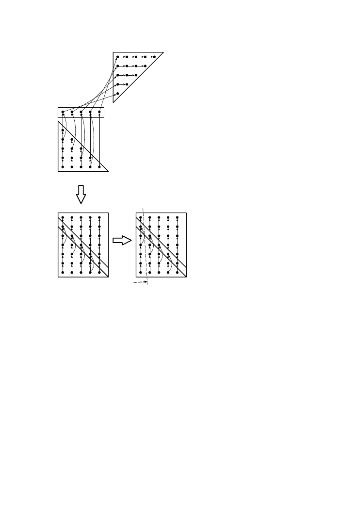
[Franssen et al. 1993; Catthoor et al. 1998]. In this model, each n-level loop
nest is represented geometrically by an n-dimensional polytope. An exam-
ple is given in Figure 1, where the loop nest at the top is two-dimensional
and has a triangular polytope representation, because the inner loop bound
is dependent on the value of the outer loop index. The arrows in the figure
represent the data dependencies; they are drawn in the direction of the
data flow. The order in which the iterations are executed can be repre-
sented by an ordering vector that traverses the polytope. To perform global
loop transformations, a two-phase approach is used. In the first phase, all
polytopes are placed in one common iteration space. During this phase, the
polytopes are considered as merely geometrical objects, without execution
semantics. In the second phase, a global ordering vector is defined in this
global iteration space. In Figure 1, an example of this methodology is given.
At the top, the initial specification of a simple algorithm is shown; at the
bottom left, the polytopes of this algorithm are placed in the common
iteration space in an optimal way, and at the bottom right, an optimal
ordering vector is defined and the corresponding code is derived.
Most existing loop transformation strategies work directly on the code.
Moreover, they typically work on single loop nests, thereby omitting the
global transformations crucial for storage and transfers. Many of these
techniques also consider the body of each loop nest as one union [Darte et
al. 1993], whereas in Franssen et al. [1993] each statement is represented
by a polytope, which allows more aggressive transformations. An exception
to the “black box” view on the loop body is formed by the “affine-by-
statement” [Darte and Robert 1992] techniques which transform each
statement separately. However, the two-phase approach still allows a more
global view on the data transfer and storage issues.
2.2 Code Rewriting Techniques to Improve Data reuse
When the system’s memory organization includes a memory hierarchy, it is
particularly important to optimize data transfers and storage to utilize the
Data and Memory Optimization
•
155
ACM Transactions on Design Automation of Electronic Systems, Vol. 6, No. 2, April 2001.
memory hierarchy efficiently. This can be achieved by optimizing the data
transfers and storage in the code to maximally expose the data reuse
possibilities. The compiler literature up to now focused on improving data
reuse by performing loop transformations (see above). But in addition to
that (important) step, we can also positively influence the behavior of the
program code on a processor with a memory hierarchy by explicitly adding
copies of subsets of the data in the source code. As far as we know, no
formal technique has been published on where to add such extra loop nests
and data copies. So code rewriting techniques, consisting of loop and data
flow transformations, are essential as a preprocessing step to achieve this,
because they significantly improve the overall regularity and access locality
of the code. This enables the next step of the platform-independent trans-
formation flow, namely, a data reuse decision step, to arrive at the desired
reduction of storage and transfers. During this step, hierarchical data
reuse copies are added to the code, exposing the different levels of reuse
that are inherently present (but not directly visible) in the transformed
code. This differs from a conventional approach where after the loop
transformation preprocessing, the hardware cache control determines the
i
j
A: (i: 1..N)::
(j: 1 .. N-i+1)::
a[i][j] = in[i][j] + a[i-1][j];
B: (p: 1..N)::
b[p][1] = f( a[N-p+1][p], a[N-p][p] );
C: (k: 1..N)::
(l: 1..k)::
b[k][l+1] = g( b[k][l] );
k
l
p
i
j
p
k
l
for (j=1; j<=N; ++j) {
for (i=1; i<=N-j+1; ++i)
a[i][j] = in[i][j] + a[i-1][j];
b[j][1] = f( a[N-j+1][j],
a[N-j][j] );
for (l=1; l<=j; ++l)
b[j][l+1] = g( b[j][l] );
}
i
j
l
Fig. 1.
Example of automatable loop transformation methodology.
156
•
P. R. Panda et al.
ACM Transactions on Design Automation of Electronic Systems, Vol. 6, No. 2, April 2001.

size and “time” of these copies based on the available locality of access. In
the Diguet et al. [1997] approach, a global exploration of the data reuse
copies is performed to globally optimize the size and timing of these copies
in the code. A custom memory hierarchy can then be designed on which
these copies can be mapped in a very efficient way (see, e.g., Wuytack et al.
[1998]). However, even for a predefined memory hierarchy, typically
present in a programmable processor context, the newly derived code from
this step implicitly steers the data reuse decisions and still results in a
major benefit to system bus load, system power budget, and cache miss
behavior (see, e.g., Kulkarni et al. [1998]). This compile-time exploration of
data reuse and code modification appears to be a unique approach not
investigated elsewhere.
Example 2.
Consider the following example, which has already under-
gone the loop transformations discussed in the previous section:
for (i
5
0; i
,
N;
11
i)
for (j
5
0; j
,5
N-L;
11
j)
b[i][j]
5
0;
for (k
5
0; k
,
L;
11
k)
b[i][j]
15
a[i][j
1
k]
;
}
When this code is executed on a processor with a small cache, it performs
much better than the initial code. To map it on a custom memory hierarchy,
however, the designer has to know the optimal size of the different levels of
this hierarchy. To this end, signal copies (buffers) are added to the code in
order to make data reuse explicit. For the example, this results in the
following code (the initialization of
a_buf
@# has been left out for simplici-
ty):
int a_buf[L]
;
int b_buf
;
for (i
5
0; i
,
N;
11
i)
initialize a_buf
for (j
5
0; j
,5
N-L;
11
j) {
b_buf
5
0;
a_buf[(j
1
L-1)%L]
5
a[i][j
1
L-1];
for (k
5
0; k
,
L;
11
k)
b_buf
15
a_buf[(j
1
k)%L];
b[i][j]
5
b_buf;
}
In this code, two data reuse buffers are present:
—a_buf
@# (L words), for the a@#@# signals
—b_buf (1 word), for the b
@#@# signals
In the general case, more than one level of data reuse buffers is possible
for each signal. A formal methodology, where all possible buffers are
arranged in a tree, is described in Wuytack et al. [1998]. Such a tree is
generated for each signal and an optimal alternative is selected.
Data and Memory Optimization
•
157
ACM Transactions on Design Automation of Electronic Systems, Vol. 6, No. 2, April 2001.

2.3 Relations Between Task and Data Parallelism
Parallelization is a standard technique used to improve the performance of
a system by using multiple processing units operating simultaneously.
However, for a given piece of code, the system’s performance can vary
widely, and there does not appear to be a straightforward solution for
effective parallelization. This is also true with respect to the impact of
parallelization on data storage and transfers. Most of the research effort in
the compiler/architecture domain addresses the problem of parallelization
and processor partitioning [Amarasinghe et al. 1995; Neeracher and Rühl
1993; Polychronopoulos 1988]. In more recent methods, data communica-
tion between processors is usually taken into account [Agarwal et al. 1995],
but they use an abstract model (i.e., a virtual processor grid, which has no
relation to the final number of processors and memories). Furthermore,
these techniques typically use execution speed as the only evaluation
metric. However, in embedded systems, power and memory size are also
important, and thus different strategies for efficient parallelization have to
be developed. A first approach for more global memory optimization in a
parallel processor context was described in Danckaert et al. [1996] and
Masselos et al. [1999b], where the authors describe an extensive precom-
piler loop reorganization phase prior to the parallelization steps.
Two important parallelization alternatives are task and data paralleliza-
tion. In task parallelization, the different subsystems of an application are
assigned to different processors. In data parallelization, each processor
executes the whole algorithm, but only on a part of the data. Hybrid
task-data parallel alternatives are also possible. When data transfer and
storage optimization is an issue, even more attention has to be paid to the
way in which the algorithm is parallelized. Danckaert et al. [1996] and
Masselos et al. [1999b] have explored this on several realistic demonstrator
examples, among which is a Quadtree Structured Difference Pulse Code
Modulation (QSDPCM) application. QSDPCM is an interframe compression
technique for video images. It involves a motion estimation step, and a
quadtree-based encoding of the motion compensated frame-to-frame differ-
ence signal. Table I shows an overview of the results when 13 processors
are used as a target, using pure data as a baseline. The estimated area and
power figures were obtained using a proprietary model from Motorola.
From this table, it is clear that the rankings for the different alternatives
(initial and transformed) are clearly distinct. For the transformed descrip-
tion, the task level oriented hybrids are better. This is true because these
kinds of partitionings keep the balance between double buffers (present in
task level partitionings) and replicates of array signals with the same
functionality in different processors (present in data level partitionings).
However it is believed that the optimal partitioning depends highly on the
number of the different submodules of the application and on the number of
processors that will be used.
With regard to the memory size required for the storage of the interme-
diate array signals, the results of the partitionings, based on the initial
158
•
P. R. Panda et al.
ACM Transactions on Design Automation of Electronic Systems, Vol. 6, No. 2, April 2001.

description, prove that this size is reduced when the partitioning becomes
more data oriented. Initially, this size is smaller for the first hybrid
partitioning (245 K), which is more data-oriented than the second hybrid
partitioning (282 K) and the task-level partitioning (287 K). However, this
can change after the transformations are applied. In terms of the number of
memory accesses to the intermediate signals the situation is simpler. The
number of accesses to these signals always decreases as the partitioning
becomes more data oriented. The table also shows the huge impact that
this platform-independent transformation stage can have on highly data-
dominated applications like this video coder. Experiments on several
processor platforms for different demonstrators [Danckaert et al. 1999]
have shown the importance of applying these optimizations.
2.4 Dynamic Memory Allocation
Embedded system designers typically use a C/C
11 based design environ-
ment in order to model embedded systems at a suitably high level of
abstraction. At this level, designers may use complex programming con-
structs that are not well understood by hardware synthesis tools. Hardware
Description Languages (HDLs) such as VHDL and Verilog offer the array
data structure as a means for specifying logical memories. However, the
modeling facilities offered by HDLs are increasingly inadequate for system-
level designers, who need the full expressive power of high-level modeling
languages. One such useful feature is dynamic memory allocation. A
system description may dynamically allocate and free memory using the
new/delete
operators and
malloc/free
function calls. Although the tasks
implied by these constructs were originally intended for an operating
system, it is possible for a hardware synthesis tool to translate them into
reasonable hardware interpretations.
Wuytack et al. [1999b] describe a system where dynamic data types are
specified at a very high abstraction level (such as association tables); these
abstract data types are then refined into synthesizable hardwarein two
main phases. In a first main phase, they are refined into concrete data
structures. For instance, an association table with two access keys can be
refined into a three-level data structure where the first level is a linked
Table I.
Overall Results for Data Memory Related Cost In QSDPCM
Version
Partitioning
Area
Power
Initial
Pure data
1
1
Pure task
0.92
1.33
Modified task
0.53
0.64
Hybrid 1
0.45
0.51
Hybrid 2
0.52
0.63
Transformed
Pure task
0.0041
0.0080
(by loop and)
Modified task
0.0022
0.0040
(data reuse)
Hybrid 1
0.0030
0.0050
(decisions)
Hybrid 2
0.0024
0.0045
Data and Memory Optimization
•
159
ACM Transactions on Design Automation of Electronic Systems, Vol. 6, No. 2, April 2001.

list, the second a binary tree, and the third one a pointer array. Each of
these three levels is accessed by subkeys that are repartitioned from the
original keys. An automated technique for this exploration is proposed in
Ykman-Couvreur et al. [1999]. In a second main phase, dynamic allocation
and freeing duties are performed by a virtual memory manager, which
performs the typical tasks involved in maintaining the free list of blocks in
memory: keeping track of free blocks, choosing free blocks, freeing deleted
blocks, splitting , and merging blocks [Wilson et al. 1995]. An exploration
technique is proposed in da Silva et al. [1998], in which different memory
allocators are generated for different data types. Following this, a basic
group splitting operation splits the memory segment into smaller basic
groups to increase the allocation freedom by, for instance, splitting an
array of structures into its constituent fields. These logical memory seg-
ments are then mapped into physical memory modules in the Storage
Bandwidth Optimization (SBO) step as described in Section 3.2.
An approach at a lower abstraction level is proposed by Semeria et al.
[2000]. It is specifically targeted to a hardware synthesis context and
assumes that the virtual memory managers are already fixed. So the
outcome of the above approach can be used directly as input for this step.
Here, the actual number and size of the memory modules are specified by
the designer, along with a hint of which
malloc
call is targeted at which
memory module. A general-purpose memory allocator module that per-
forms the block allocation and freeing tasks is also instantiated for each
memory module. However, the allocator can be optimized and simplified
when the size arguments to all
malloc
calls for a single module are
compile-time constants and when constant-size data is allocated and freed
within the same basic block. In the latter case, the dynamic allocation is
replaced by a static array declaration.
2.5 Memory Estimation
Estimation techniques that assess the memory requirements of an applica-
tion are critical for helping the system designer select a suitable memory
realization. At the system level, no detailed information is available about
the size of the memories required for storing data in alternative realiza-
tions of an application. To guide the designer and help in choosing the best
solution, estimation techniques for storage requirements are therefore
needed very early in the system design trajectory. For data-dominant
applications, the high-level description is typically characterized by large
multidimensional loop nests and arrays. A straightforward memory size
estimate can be computed by multiplying the dimensions of individual
arrays and summing up the sizes of different arrays. However, this could
result in a huge overestimate, since not all the arrays, and certainly not all
parts of one array, are alive at the same time. In this context an array
element, also denoted a signal, is alive from the moment it is written, or
produced, until it is read for the last time. This last read is said to consume
the element [Aho et al. 1993]. Since elements with nonoverlapping lifetimes
160
•
P. R. Panda et al.
ACM Transactions on Design Automation of Electronic Systems, Vol. 6, No. 2, April 2001.

can share the same physical memory location (the in-place mapping prob-
lem [Verbauwhede et al. 1989]), a more accurate estimate has to account
for mapping arrays and parts of arrays to the same place in memory. To
what degree it is possible to perform in-place mapping depends heavily on
the order in which the elements in the arrays are produced and consumed.
This is mainly determined by the execution ordering of the loop nests
surrounding the instructions accessing the arrays.
At the beginning of the design process, little information about the
execution order is known. Some is given from the data dependencies
between the instructions in the code, and the designer may restrict the
ordering for example, due to I/O constraints. In general, however, the
execution order is not fixed, giving the designer considerable freedom in the
implementation. As the process progresses, the designer takes decisions
that gradually fix the ordering, until the full execution ordering is known.
To steer this process, estimates of the upper and lower bounds on the
storage requirement are needed at each step, given the partially fixed
execution ordering.
The storage requirements for scalar variables can be determined by a
clique partitioning formulation for performing register allocation (described
in Section 3.1.1). However, such techniques break down for large multidi-
mensional arrays, due to the huge number of scalars present when each
array element is treated as a scalar. To overcome this shortcoming, several
research teams have tried to split the arrays into suitable units before or as
a part of the estimation. Typically, each instance of array element access-
ing the code is treated separately. Due to the code’s loop structure, large
parts of an array can be produced or consumed by the same code instance.
This reduces the number of elements the estimator must handle compared
to the scalar approach.
Verbauwhede et al. [1994] use a production time axis to find the maxi-
mum difference between the production and consumption times for any two
dependent instances, giving the storage requirement for one array. The
total storage requirement is the sum of the requirements for each array.
Only in-place mapping internal to an array is considered, not the possibil-
ity of mapping arrays in place of each other. In Grun et al. [1998], the data
dependency relations between the array references in the code are used to
find the number of array elements produced or consumed by each assign-
ment. From this, a memory trace of upper and lower bounding rectangles
as a function of time is found with the peak bounding rectangle indicating
the total storage requirement. If the difference between the upper and
lower bounds for this critical rectangle is too large, the corresponding loop
is split into two and the estimation is rerun. In the worst-case situation, a
full loop unrolling is necessary to achieve a satisfactory estimate, which
can become expensive. Zhao and Malik [1999] describe a methodology based
on live variable analysis and integer point counting for intersection/union
of mappings of parameterized polytopes. They show that it is only neces-
sary to find the number of live variables for one instruction in each
innermost loop nest to get the minimum memory size estimate. However,
Data and Memory Optimization
•
161
ACM Transactions on Design Automation of Electronic Systems, Vol. 6, No. 2, April 2001.
the live variable analysis is performed for each iteration of the loops, which
makes it computationally hard for large multidimensional loop nests. A
major limitation for all of these techniques is their requirement of a fully
fixed (imperative) execution ordering.
In contrast to the methods described in the previous paragraph, the
storage requirement estimation technique presented by Balasa et al. [1995]
does not assume an execution ordering. It starts with an extended data
dependency analysis, resulting in a number of nonoverlapping basic sets of
array elements and the dependencies between them. The size of the
dependency is the number of elements consumed (read) from one basic set
while producing the dependent basic set. The maximal combined size of
simultaneously alive basic sets gives the storage requirement.
The high-level estimation methodology described by Kjeldsberg et al.
[2000b] goes a step further, and takes into account partially fixed execution
ordering, achieved by an array data flow analysis preprocessing [Feautrier
1991; Pugh and Wonnacott 1993].
Example 3.
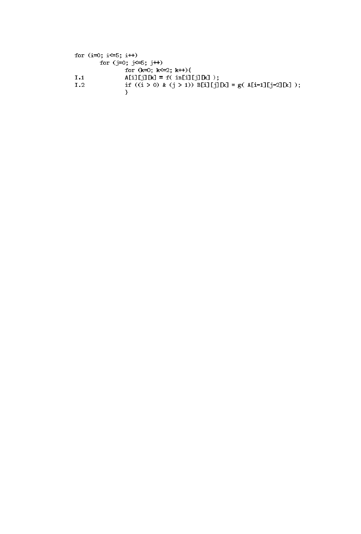
Consider the simple application code example shown in
Figure 3. Two instructions, I.1 and I.2, produce elements of two arrays, A
and B. Elements from array A are consumed when elements of array B are
produced. This gives rise to a flow type data dependency between the
instructions [Banerjee 1998].
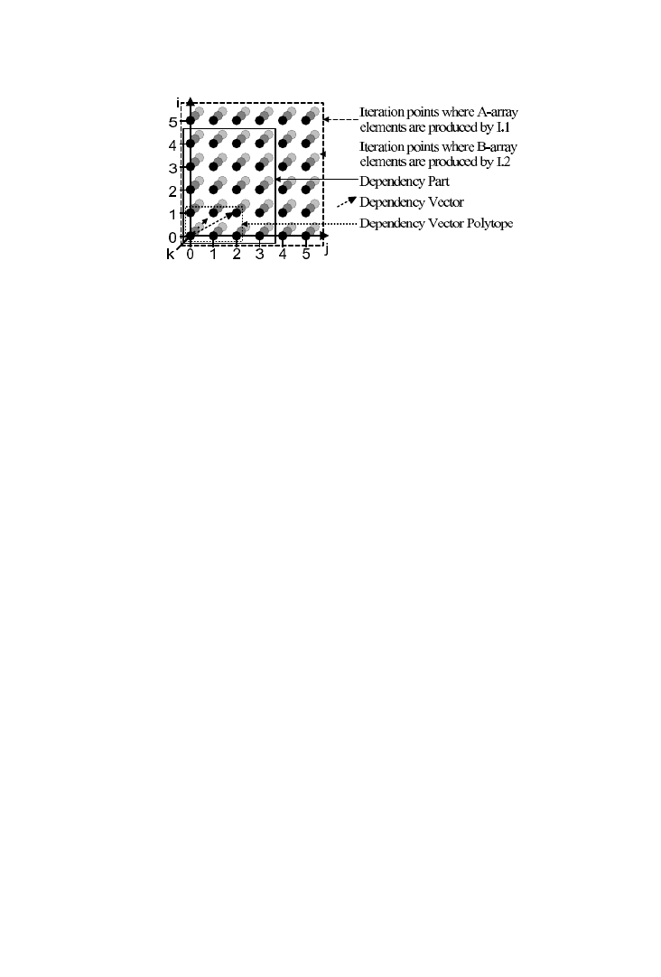
The loops around the operations define an iteration space [Banerjee
1998], as shown in Figure 3. Each point within this space represents one
execution of the operations inside the loop nest. For our example, at each of
these iteration points, one A-array element and, when the if clause condi-
tion is true, one B-array element is produced. In general, not all elements
produced by one operation are read by a depending operation. A depen-
dency part (DP) is defined containing all the iteration points for which
elements that are read by the depending operation are produced. Next, a
dependency vector (DV) is drawn from any iteration point in the DP
producing an array element to the iteration point producing the depending
element. This DV is usually drawn from the point in the DP that is nearest
to the origin. Finally, the chosen DV spans a rectangular dependency vector
polytope (DVP) in the N-dimensional space with sides parallel to the
iteration space axes. The N dimensions of this DVP are defined as spanning
dimensions (SD). Since normally the SD only comprises a subset of the
iterator space dimensions, the remaining dimensions are denoted nonspan-
ning dimensions (ND), but this set can be empty. For the DVP in Figure 3,
i and j are SDs while k is ND.
Fig. 2.
Simple application code example in C.
162
•
P. R. Panda et al.
ACM Transactions on Design Automation of Electronic Systems, Vol. 6, No. 2, April 2001.
Using the concepts above, Kjeldsberg et al. [2000a] describe the details of
the size estimates of individual dependencies. The main contribution is the
use of the DP and DVP for calculating the upper and lower bounds on the
dependency size, respectively. As the execution ordering is fixed gradually
during the design phases, dimensions and array elements are removed
from the DP or added to the DVP to comprise tighter bounds until they
converge for a fully fixed ordering. Whether dimensions and array elements
are removed from the DP or added to the DVP is, in general, decided by the
partial fixation of spanning and nonspanning dimensions. It has been
shown that the size of a dependency is minimized if spanning dimensions
are fixed innermost and nonspanning dimensions outermost. Table II
summarizes estimation results for the dependency in Figure 3 for a number
of partially fixed execution orderings. The results are compared with those
achieved with the methodology in Balasa et al. [1995] where the execution
ordering is ignored, and with manually calculated exact results for best-
case (BC) and worst-case (WC) ordering.
In order to achieve a global view of the storage requirements for an
application, the combined size of simultaneously alive dependencies must
be taken into account [Kjeldsberg et al. 2000b]; but this falls outside the
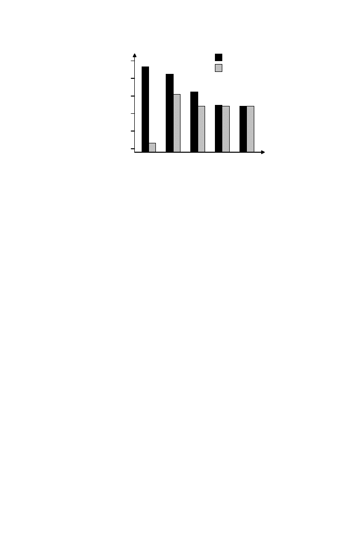
scope of this survey. Applying this approach to the MPEG-4 [The ISO/IEC
Moving Picture Experts Group 2001], the motion estimation kernel demon-
strates how the designer can be guided in applying the critical early loop
transformations to the source code. Figure 4 shows estimates of upper and
lower bounds on the total storage requirement for two major arrays. In
Step (a) no ordering is fixed, leaving a large span between the upper and
lower bounds. At (b), one dimension is fixed outermost in the loop nest,
resulting in big changes in both upper and lower bounds. For step (c), an
alternative dimension is fixed outermost in the loop nest. Here the reduc-
tion of the upper bound is much larger than in (b), while the increase of the
lower bound is much smaller. Even with such limited information, it is
possible for the designer to conclude that the outer dimension used in (c) is
better than the one used in (b). At (d), there is an additional fixation of a
second outermost dimension with a reduced uncertainty in the storage
requirement as a result. Finally at step (e), the execution ordering is fully
Fig. 3.
Iteration space with dependency part, dependency vector, and dependency vector
polytope.
Data and Memory Optimization
•
163
ACM Transactions on Design Automation of Electronic Systems, Vol. 6, No. 2, April 2001.

fixed. The estimation results guide the designer towards an optimized
solution.
3. MEMORY MODELING, CUSTOMIZATION, AND OPTIMIZATION
In the previous section we outlined various source-level transformations
that guarantee improved memory characteristics of the resulting imple-
mentation, irrespective of the target memory architecture. We now survey
optimization strategies designed for target memory architectures at vari-
ous levels of granularity, starting from registers and register files to
SRAM, cache, and DRAM.
3.1 Memory Allocation in High-Level Synthesis
In this section we discuss several techniques for performing memory
allocation in high-level synthesis (HLS) research. The early techniques
generally assumed that the scheduling phase of HLS, which assigns opera-
tions in a data flow graph (DFG) had already been performed. Following
scheduling, all variables that need to be preserved over more than one
control step are stored in registers. The consequent optimization problem,
called register allocation [Gajski et al. 1992], is the minimization of the
number of registers assigned to the variables because the register count
impacts the area of the resulting design.
3.1.1 Register Allocation by Graph Coloring.
Early research efforts on
register allocation can ultimately be traced back to literature on compiler
technology. Chaitin et al. [1981] present a graph coloring-based heuristic
for performing register allocation. The life time [Aho et al. 1993] of each
variable is computed first, a graph is constructed whose nodes represent
variables, and the existence of an edge indicates that the life times overlap,
i.e., they cannot share the same register; a register can only be shared by
variables with nonoverlapping life times. Thus, the problem of minimizing
the register count for a given set of variables and their life times is
equivalent to the graph coloring problem [Garey and Johnson 1979]: assign
colors to each node of the graph such that the total number of colors is
minimum and no two adjacent nodes share the same color. This minimum
number is called the chromatic number of the graph. In the register
Table II.
Dependency Size Estimates of a Simple Example (in number of scalar
dependencies)
Fixed Dimension(s)
Lower
bound
Upper
bound
Balasa et
al. ’95
Exact BC/WC
Outermost
Innermost
None
4
36
60
6/23
k
4
12
60
6/11
k,i
31
31
60
6/11
j
6
14
60
6/14
i, j
6
6
60
6/6
k,i, j
6
6
60
6/6
164
•
P. R. Panda et al.
ACM Transactions on Design Automation of Electronic Systems, Vol. 6, No. 2, April 2001.
allocation problem, the minimum register count is equal to the chromatic
number of the graph and each color represents a different physical register.
Graph coloring is a well-known NP-complete problem, so an appropriate
approximation algorithm is generally employed. Tseng and Siewiorek
[1986] formulate the register allocation problem with the clique partition-
ing problem: partition a graph into the minimum number of cliques or fully
connected subgraphs. This problem is equivalent to graph coloring (if a
graph
G has a chromatic number
x, then its complement graph G9 can be
partitioned into a minimum number of
x cliques). Their greedy heuristic
initially creates one clique for each node, then proceeds by merging
individual cliques into a larger one, selecting at each step to merge those
cliques that have the maximum number of common neighbors.
A polynomial time solution to the register allocation problem was pre-
sented by Kurdahi and Parker [1987]. They apply the left-edge algorithm to
minimize the register count by first sorting the life time intervals of the
variables in order of their start times and then making a series of passes,
each pass allocating a new register and assigning nonoverlapping intervals
from the sorted set to the register. This algorithm guarantees the minimum
number of registers for straight-line code with no branches and runs in
polynomial time. The register allocation problem has also been formulated
as a bipartite graph-matching, where the edges are weighted with the
expected interconnect cost [Huang et al. 1990].
Subsequent refinements to the register allocation problem in HLS were
based on a higher level of design abstraction—the target architecture was a
register file with a fixed number of ports, rather than scattered individual
registers. A critical problem in the presence of loops is how to deal with
data that exhibits dependencies accross the loop iterations. This was solved
with cyclic approaches such as those in Goossens et al. [1989]. A good
survey of scalar approaches is provided by Stok and Jess [1992].
3.1.2 Allocating Scalar Variables to Single and Multiport Memories.
A
new optimization problem arises when individual registers are replaced by
45312
17664
1664
1026
2
257
257
257
300
260
100000
10000
1000
100
10
1
Upper Bound
Lower Bound
a)
b)
c)
d)
e)
Fig. 4.
Storage requirement of the ME kernel.
Data and Memory Optimization
•
165
ACM Transactions on Design Automation of Electronic Systems, Vol. 6, No. 2, April 2001.
a register file or a memory module. The registers (or memory locations) can
no longer all be accessed simultaneously; the number of allowed simulta-
neous accesses is limited to the number of available ports in the memory.
This results in a stronger interaction of the memory allocation decision
with the scheduling phase of HLS.
Balakrishnan et al. [1988] present a technique to allocate multiport
memories in HLS. To exploit the increased efficiency of grouping several
registers into a single multiport memory, the technique attempts to merge
registers with disjoint access times. While clique partitioning is sufficient
to handle the case of a single port memory, a more general framework is
needed to handle multiport memories. The technique formulates a 0-1
linear programming problem by modeling the port types (read, write, and
read/write), the number of ports, and the accesses scheduled to each
register in each control step. Since the linear programming problem is
NP-complete, a branch-and-bound heuristic is employed.
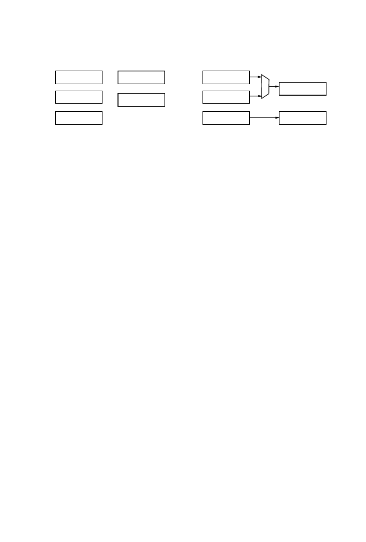
Example 4.
Consider a scheduled sequence with states S1 and S2
involving three registers R1, R2, and R3 to be mapped into a dual-port
memory:
S1 : R1
4 R2
1 R3
S2 : R2
4 R1
1 R1
The use of registers at each control step is shown in Figure 5. To
determine which registers to group into the 2-port memory, we need to
solve the following problem:
maximize
~x
1
1 x
2
1 x
3
!
under the constraints
x
1
1 x
2
1 x
3
# 2
x
1
1 x
2
# 2
where
x
i
is 0 or 1, depending on whether register R
i is assigned to the
multiport memory. In this example, the solution is
x
1
5 1, x
2
5 1, x
3
5 0.
That is, the maximal set of registers that can be assigned to the memory
R1
R2
R3
R1
R2
S1
S2
Fig. 5.
Use of registers in each control step.
166
•
P. R. Panda et al.
ACM Transactions on Design Automation of Electronic Systems, Vol. 6, No. 2, April 2001.

while obeying the constraints is
$R1, R2%. The procedure can then be
repeated for assigning the remaining registers to other multiport memories.
However, the sequentialization of the memory assignment does not lead
to the minimum number of memory modules. In order to minimize the total
number of multiport memories, the memories themselves need to be
incorporated into the problem formulation. Ahmad and Chen [1991] de-
scribe MAP, a generalization of the 0-1 integer linear programming (ILP)
problem that performs this minimization.
The relative cost benefits of storing data in discrete registers or SRAM
modules is performed by Kramer and Muller [1992] in the context of
allocating storage for global signals while synthesizing multiple VHDL
processes. Area and performance tradeoffs involved in parallel accesses due
to storage in discrete registers and sequential accesses due to storage in
RAM are performed while generating the clustering solution for registers.
The allocation of scalar variables to register files or multiport memories
results in a significant advantage over discrete registers – the interconnect
cost of the resulting circuit is reduced drastically. Further, there may be an
additional interconnect optimization opportunity when the multiport regis-
ter file allows us to optionally connect each register to only those ports that
are necessary. This decision impacts the number of interconnections be-
tween the functional units and memory ports, and the related optimization
problem is to minimize this number in order to reduce chip area.
Both memory allocation strategies described above propose 0-1 ILP
formulations for reducing the interconnect cost. Kim and Liu [1993] reverse
the memory allocation and interconnect minimization steps, reasoning that
the interconnect cost is dominant in determining chip area. Lee and Hwang
[1995] present a method to handle the memory allocation decision during
HLS scheduling rather than as a postprocessing step by weighting the
priority function used by the list scheduling algorithm [Gajski et al. 1992]
to attempt equal distribution of memory data transfers in the control steps.
3.1.3 Modeling Memory Accesses in HLS.
The memory allocation tech-
niques discussed earlier used a simple model of memory accesses: data is
read from memory; computations are performed; and data is written back
to memory in the same clock cycle. This model works for registers and
small registers files. However, when data is stored in a reasonably large
on-chip SRAM, the access times are higher and significant compared to the
computation time. Accessing memory data may actually require one or
more clock cycles. Clearly, the scheduling model of memory accesses needs
to be updated to handle this more complex protocol.
The behavioral template scheduling model by Ly et al. [1995] offers a way
of handling memory accesses that is consistent with the way other opera-
tions are viewed by the scheduler. Every operation is represented by a
template; complex operations may take multiple cycles in the template,
with different stages representing local scheduling constraints among the
stages. Behavioral templates can be used to model memory accesses, as
Data and Memory Optimization
•
167
ACM Transactions on Design Automation of Electronic Systems, Vol. 6, No. 2, April 2001.
shown in Figure 6. The Synopsys behavioral compiler tool [Synopsys Inc.
1997] uses this template concept to perform scheduling. Extensions of this
modeling methodology to handle more complex memory access protocols
(e.g., DRAMs) are presented in Section 3.8.
3.2 Ordering and Bandwidth Reduction
In many cases, a fully customized memory architecture can give superior
memory bandwidth and power characteristics over traditional hierarchical
memory architecture that includes data caches. This is particularly true
when the application is amenable to detailed compile time analysis.
Although a custom memory organization has the potential to signifi-
cantly reduce the system cost, achieving these cost reductions is not trivial,
especially manually. Designing a custom memory architecture means de-
ciding how many memories to use and of which type (single-port, dual-port,
etc). In addition, memory accesses have to be ordered in time, so that the
real-time constraints (the cycle budgets) are met. Finally, each array must
be assigned to a memory, so that arrays can be accessed in parallel, as
required to meet real-time constraints [Cathoor et al.1998]. These issues
are relevant and have a large impact on the memory bandwidth and power,
even when the basic memory hierarchy is fixed, e.g.. based on two cache
levels and DRAM memory: modern low-power memories [Itoh et al.1995]
allow much customization, certainly in terms of bank assignment (e.g.,
SDRAMs), sizes, or ports (e.g., several modern SDRAMs).
One important factor that affects the cost of the memory architecture is
the relative ordering of the memory accesses contained in the input
specification. Techniques for optimizing the number of resources given the
cycle budget are relevant in the scheduling domain, as are most of the early
techniques that operate on the scalar-level [Pauwels et al. 1989]. Many of
these scalar techniques try to reduce the memory related cost by estimating
the required number of registers for a given schedule, but this does not
scale for large array data. The few exceptions published are the stream
scheduler [Verhaegh et al. 1996; 1995], the rotation scheduler [Passos et al.
1995] and the percolation scheduler [Nicolau and Novack 1993]. They
R0
R1
W0
W1
Address
Address
Data
Memory Read
Memory Write
Fig. 6.
Scheduling template for RAM accesses: 2-cycle memory read and 2-cycle memory
write. The address needs to be valid for both cycles. For memory write, the data needs to be
ready by the second cycle.
168
•
P. R. Panda et al.
ACM Transactions on Design Automation of Electronic Systems, Vol. 6, No. 2, April 2001.

schedule both accesses and operations in a compiler-like context, but with
more emphasis on the cost and performance impact of the array accesses,
and also include a more accurate model of their timing. Only a few of them
try to reduce the required memory bandwidth by minimizing the {number}
of simultaneous data accesses [Verhaegh et al. 1996]. They do not take into
account which data is being accessed simultaneously. Also, no real effort is
made to optimize the data access conflict graphs such that subsequent
register/memory allocation tasks can do a better job.
The scheduling freedom among memory accesses can also be exploited to
generate memory architectures with lower cost (number of memories) and
lower bandwidth (number of ports). This issue is addressed with the
storage bandwidth optimization (SBO) technique and the associated stor-
age cycle budget distribution (SCBD) step by Wuytack et al. [1999a].
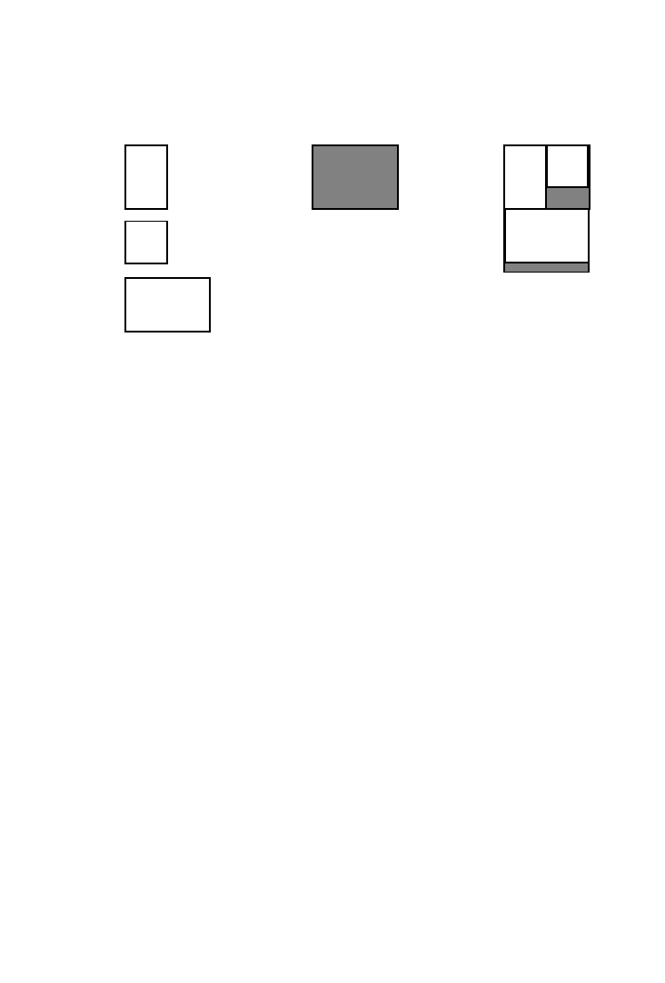
Example 5.
Suppose the data flow graph shown in Figure 7(a) has to be
scheduled with a time constraint of six cycles. Each access requires one
cycle. A satisfying schedule that minimizes the number of simultaneous
memory accesses is shown in Figure 7(b). Surprisingly, this schedule leads
to a sub-optimal implementation. Figure 7(c) shows a conflict graph for this
schedule, where each node represents an array and an edge between nodes
indicates that the two are being accessed in parallel in some control step.
The significance of the edge is that the nodes need to be assigned to
different single port memories (analogous to the register allocation prob-
lem) or different ports of the same multiport memory, both expensive
alternatives. A coloring of the graph reveals a chromatic number of 3, i.e.,
three single port memories are required to satisfy all the conflicts. How-
ever, consider the alternative schedule of Figure 7(e) and the corresponding
graph of Figure 7(f). This graph has a chromatic number of 2, resulting in
the simpler and lower cost memory assignment of Figure 7(g). This exam-
ple demonstrates that the relative ordering of the memory accesses has a
significant impact on the memory cost.
The condition of the same array being accessed multiple times in the
same control step is represented by self-loops in the conflict graph, and
leads to multiport memory implementations. An iterative conflict-directed
ordering step generates a partial ordering of the CDFG that minimizes the
required memory bandwidth.
This SCBD step has to be followed by a memory allocation and array-to-
memory assignment step as described in the next section.
3.3 Memory Packing and Array-to-Memory Assignment
In a custom memory architecture, the designer can choose memory param-
eters such as the number of memories, and the size and number of ports in
each memory. This decision, which takes into account the constraints
derived in the previous section, is the focus of the memory allocation and
assignment (MAA) step. The problem can be subdivided into two subprob-
lems. First, memories must be allocated: a number of memories are chosen
Data and Memory Optimization
•
169
ACM Transactions on Design Automation of Electronic Systems, Vol. 6, No. 2, April 2001.
from the available memory types and port configurations. But the dimen-
sions of the memories are determined only in the second stage. When
arrays are assigned to memories, their sizes can be added and the maximal
bit-width can be taken to determine the required size and bit-width of the
memory. With this decision, the memory organization is fully determined.
Allocating more or fewer memories has an effect on the chip area and on
the energy consumption of the memory architecture (see Fig. 8). Large
memories consume more energy per access than small memories, due to the
longer word- and bit-lines. So the energy consumed by a single large
memory containing all the data is much larger than when the data is
distributed over several smaller memories. Also, the area of the one-
A
B
A
B
C
C
D
D
A
C
B
time
B
A
C
D
A
B
D
C
RA
RB
RC
RC
WB
RD
RA
WD
WA
WC
WC
(a)
(b)
A
B
A
B
C
C
D
D
A
C
B
time
B
A
C
D
A
B
D
C
(c)
(d)
(e)
(f)
(g)
Fig. 7.
Storage bandwidth optimization: (a) data flow graph; (b) candidate schedule; (c)
conflict graph; (d) memory assignment; (e) alternate schedule; (f) new conflict graph; (g) new
assignment.
170
•
P. R. Panda et al.
ACM Transactions on Design Automation of Electronic Systems, Vol. 6, No. 2, April 2001.
memory solution is often higher when different arrays have different
bit-widths. For example, when a 6-bit and an 8-bit array are stored in the
same memory, two bits are unused for every 6-bit word. By storing the
arrays in different memories, one 6 bits wide and the other 8 bits wide, this
overhead can be avoided.
The other end of the spectrum is to store all the arrays in different
memories. This also leads to relatively high energy consumption, due to the
increase in the external global interconnection lines connecting all these
(small) memories to each other and to the data-paths. Likewise, the area
occupied by the memory system goes up, due to the interconnections and to
the fixed address decoding and other overhead per memory.
Clearly, the interesting memory allocations lie somewhere between the
two extremes. The area and the energy function reach a minimum in
between, but at different points. The useful exploration region to tradeoff
area with energy consumption lies in between the two minima [Brockmeyer
et al. 2000b].
The cost of memory organization does not depend on the allocation of
memory only, but also on the assignment of arrays to the memories (the
discussion above assumes an optimal assignment). When several memories
are available, many ways exist to assign the arrays to them. In addition to
the conflict cost mentioned earlier, the optimal assignment of arrays to
memories depends on the specific memory types used. For example, the
energy consumption of some memories is very sensitive to their size, while
for others it is not. In the former case, it may be advantageous to accept
some wasted bits in order to keep the heavily accessed memories very
small, and vice-versa.
A lot of research in recent years has concentrated on the general problem
of how to efficiently store data specified in an abstract specification into a
given target memory architecture. Both the specification as well as the
Cost
Allocation
B
C
D
Chrom. Nr. = 3
D
C
A
C
D
A
B
B
Chrom. Nr.
Nr. Signals
Power
Power (without interconnect)
Area
3 mem.
4 mem.
Periphery (&interconnect)
Interconnect
Bit waste
Large memories
Area
Power
A
Fig. 8.
Tradeoff between number of memories and cost during allocation and assignment.
Data and Memory Optimization
•
171
ACM Transactions on Design Automation of Electronic Systems, Vol. 6, No. 2, April 2001.
target architecture tend to be widely varying in different design contexts,
leading to many different approaches to solve the problem. The usual
assumption is that the embedded environment has no virtual memory
system, and the compiler/ synthesis tool can statically assign data to actual
memory locations.
The memory packing problem occurs when a set of memories from the
designer’s point of view (logical memories) have to be assigned to a given
set of memory modules (physical memories) while respecting certain con-
straints on the performance of the overall system or minimizing an optimi-
zation criterion such as the total delay, area, or power dissipation.
The packing problem was first considered by Karchmer and Rose [1994]
in the context of an FPGA where the number and access times of the
available physical memories are fixed and the logical memories, which are
associated with a required data access rate, have to be assigned to these
physical memories while satisfying the access time requirements. Mapping
multiple logical memories to the same physical memory would, in this
formulation, cause a multiplexing of the data access, thereby reducing the
actual access rates. For example, if two logical memories are mapped into
the same physical memory with access time 10 ns, then the effective access
time for both memories would double to 20 ns. This scenario is relevant in
stream-based systems.
Example 6.
Suppose we have an application with the logical memory
requirements shown in Figure 9(a): two
2K
3 7 memories and one 5K 3
8 memory with the maximum access times of 30 ns and 10 ns, respectively.
A
2K
3 7 memory refers to a memory with 2K words with bit width 7.
There are two
8K
3 8 physical memories available on the FPGA.
A possible solution is shown in Figure 9(b). The two
2K
3 7 logical
memories are assigned to one
8K
3 8 physical memory with the effective
access time of 20 ns, which satisfies the access time requirements of the
system.
The logical memories need to be split when either the bit-width or the
word count exceeds that of the available physical memories. In the Mem-
Packer utility presented by Karchmer and Rose [1994], the memory map-
ping problem is solved by a branch-and-bound algorithm that attempts to
minimize the estimated area of the memory subsystem. The decision tree is
Logical Memories
Solution
2K x 7 @ 30 ns
2K x 7 @ 30 ns
5K x 8 @ 10 ns
5K x 8 @ 10 ns
8K x 8 @ 10 ns
2K x 7 @ 20 ns
2K x 7 @ 20 ns
8K x 8 @ 10 ns
8K x 8 @ 10 ns
8K x 8 @ 10 ns
Physical Memories
Fig. 9.
Mapping logical memories to physical ones while satisfying required access rates.
172
•
P. R. Panda et al.
ACM Transactions on Design Automation of Electronic Systems, Vol. 6, No. 2, April 2001.
pruned when an illegal packing is encountered, i.e., when an assignment
violates the access time requirements.
The MemPacker algorithm assumes that the required size and data
access times required for the logical memories is known a priori. However,
this assumption is not always correct. When memory allocation forms part
of an automated synthesis framework, the required access times, etc., have
to be inferred from the user specification and constraints on the overall
system. The MeSA algorithm [Ramachandran et al. 1994] attempts to
integrate the memory allocation step with array clustering (grouping of
behavioral arrays into the same physical memory) into a behavioral synthe-
sis framework.
Example 7.
An example behavioral statement and the impact of array
clustering on the architecture and schedule sre shown in Figure 10. There
is an area and performance overhead arising from the additional multiplex-
ers and registers. The MeSA algorithm uses a hierarchical clustering
approach and a detailed model of the memory area to evaluate the impact
of candidate architectures.
Behavior
int A [1000]
int B [1000]
...
B[k] = A[i] + A[j]
A
B
+
i
k
R
j
S1: R = A[i] + A[j]
S2: B[k] = R
S1: R1 = A[i]; R2 = A[j]; j’ = k + 1000
S2: B[j’] = R1 + R2
A
+
i
j
k
1000
j’
B
R1
R2
No Clustering
Clustering
Fig. 10.
Array clustering in MeSA.
Data and Memory Optimization
•
173
ACM Transactions on Design Automation of Electronic Systems, Vol. 6, No. 2, April 2001.
A framework for clustering array variables into memories is presented in
the ASSASYN tool [Schmit and Thomas 1997], which recognizes that the
packing can actually be done in two dimensions. Apart from mapping
arrays into distinct memory addresses of the same memory module (vertical
concatenation), two arrays can also be packed so that corresponding ele-
ments occupy different bit ranges in the same physical word (horizontal
concatenation) if the sum of the required bit-widths of the arrays is less
than or equal to the bit-width of the physical memory. An example is shown
in Figure 11. The
a and b are packed horizontally while a and c are packed
vertically. ASSASYN has at its core a set of move transformations that
generate candidate architectures in a simulated annealing-based optimiza-
tion framework.
A general scheme for solving the memory packing problem that takes the
bit-width, word count and the number of ports into consideration was
included in the HLLM (high-level library mapping) approach of Jha and
Dutt [1997]. They present exhaustive solutions as well as linear-time
approximations to combine three separate tasks: bit-width mapping, word
mapping, and port mapping. Bakshi and Gajski [1995], present a technique
for reducing memory cost in a memory selection algorithm that attempts to
combine memory allocation and pipelining in an attempt to reduce memory
cost. A hierarchical clustering technique is used here, too, in order to group
DFG nodes into the same memory module.
A recursive strategy of memory splitting (resulting in a distributed
assignment) starting from a single port solution for a sequential program
was proposed in Benini et al. [2000].
The automated memory allocation and assignment (MAA) step, including
the organization of arrays in the physical memories before scheduling or
procedural ordering are fully fixed, is addressed in Balasa et al. [1994], and
has been coupled to the (extended) conflict graph discussed above [Slock et
al. 1997]. The resulting techniques lead to a significantly extended search
Logical Memories
a
b
c
a
b
c
Physical Memory
Assignment
Fig. 11.
Horizontal and vertical concatenation.
174
•
P. R. Panda et al.
ACM Transactions on Design Automation of Electronic Systems, Vol. 6, No. 2, April 2001.

space for memory organization solutions, which is effectively explored in
the HIMALAIA tool [Vandecappelle et al. 1999]. An alternative MAA
approach based on conflict graphs is proposed in Shiue et al. [2000].
3.4 Memory Access Time versus Cost Exploration Using Pareto Curves
By combining the SCBD and MAA steps of the previous sections, we can
effectively explore and tradeoff different solutions in the performance,
power, and area space [Brockmeyer et al. 2000a]. Indeed, every step of the
SCBD-MAA combination generates a set of valid solutions for a different
cycle budget. Hence it becomes possible to make the right tradeoff within
this solution space. Note that without automated tool support, the type of
tradeoffs discussed here are not feasible on industrial-strength applica-
tions, and thus designers may miss the opportunity to explore a larger
design space.
When the input behavior has a single thread and the goal is to reduce
power, the tradeoff can be based solely on tool output. The given cycle
budget defines a conflict graph that can be used for the MAA tool [Vande-
cappelle et al. 1999]. Obviously, the power and area costs increase when
the cycle budget is lowered: more bandwidth is needed, which requires
multiport memories (increases power) or more memories (increases area).
This is illustrated in a binary tree predictive coding (BTPC) application, a
lossless or lossy image compression algorithm based on multiresolution
that involves a complex algorithm. The platform-independent code trans-
formation steps [Catthoor et al. 1998], discussed in Section 2, are applied
manually in this example and the platform-dependent steps (using tools)
give accurate feedback about performance and cost [Vandecappelle et al.
1999]. Figure 12 shows the relation between speed and power for the
original, optimized and intermediate transformed specifications. The off-
chip signals are stored in separate memory components. Four memories are
allocated for the on-chip signals. Every step leads to a significant perfor-
mance improvement without increasing the system cost. For every descrip-
tion, the cycle budget can be traded for system cost, demonstrating the
significant effect of the platform-independent code transformation [Brock-
meyer et al. 2000b].
This performance-power function, when generated per task, can be used
to tradeoff cycles assigned to a task at the system level. Assigning too few
cycles to a single task causes the entire application to perform poorly. The
cycle and power estimates help the designer to assign tasks to processors
and to distribute the cycles within the processors over various tasks
[Brockmeyer et al. 2000a]. Minimizing the overall power within a processor
is possible by applying function minimization on all the power-cycle func-
tions together.
The interaction of the datapath power/performance with the memory
system creates another level of tradeoffs. The assignment of cycles to
memory accesses and to the data-path is important for overall power
consumption. A certain percentage of the overall time can be spent on
Data and Memory Optimization
•
175
ACM Transactions on Design Automation of Electronic Systems, Vol. 6, No. 2, April 2001.
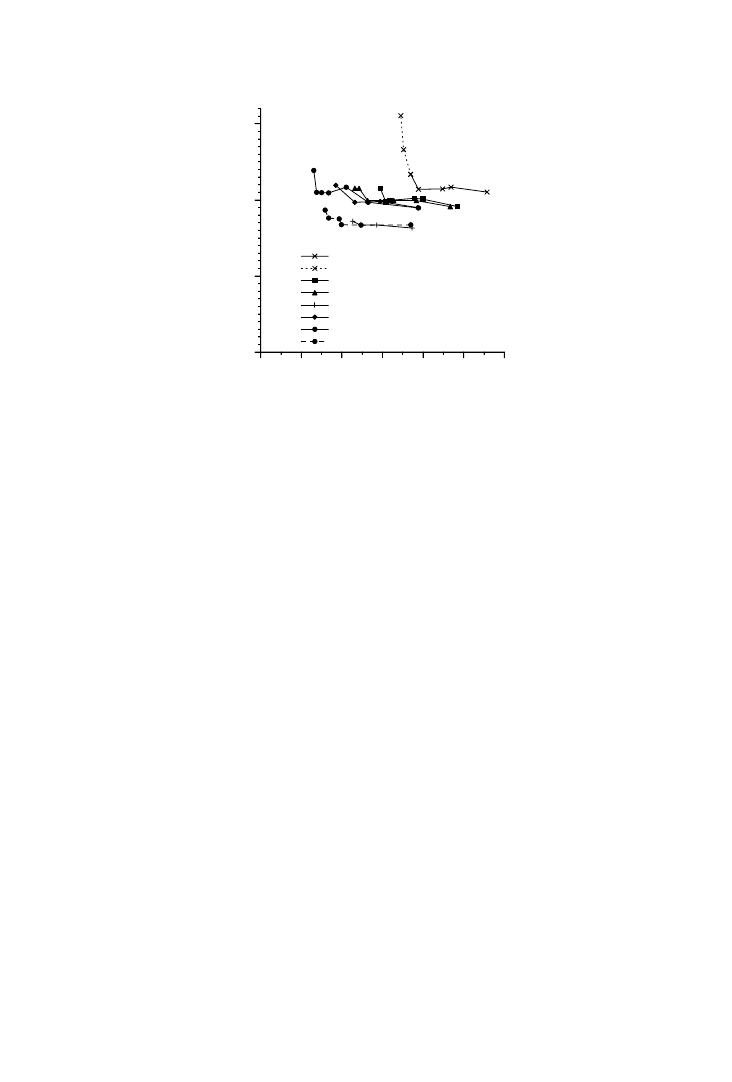
memory accesses and the remaining time on computational issues, taking
system pipelining into account (see Fig. 13). The data path cost versus
performance tradeoff is well known: when fewer cycles are available, more
hardware is needed and more power is consumed (dotted curve). The tools
discussed in Brockmeyer et al. [2000b] can provide the other half of the
graph, namely the memory-related cost (solid curve). Combining the two,
leads to an optimized implementation (dashed curve).
3.5 Reducing Bus Transitions for Low Power
Most area and performance optimizations we have discussed so far also
indirectly reduce power dissipation. For example, reducing the number of
memory modules from two to one not only reduces area, but also reduces
power dissipation because the data and address buses, which consist of
high capacitance wires, are now fewer and shorter. Similarly, performance
optimizations that reduce the number of memory accesses also reduce
power as a side effect, due to reduced switching on the memory circuitry
and address/data buses. However, certain classes of optimizations are
explicitly targeted at reducing power dissipation, even at the expense of
additional area or performance cost. We discuss techniques that attempt to
reduce switching activity on the memory address and data bus while
keeping the number of memory accesses unchanged. The extra computation
typically introduces a negligible additional switching activity, compared to
the power savings from reduced bus activity. As observed by Panda and
Dutt [1999], typical switching of off-chip buses causes three orders of
magnitude more energy than on-chip wires.
Minimizing transition activity on memory buses can be effected by two
different approaches: encoding and data organization.
0
5
10
15
20
25
30
Cycle budget (#Mcycles)
0
100
200
300
P
o
wer (mW)
4 on-chip memories
Original
Original, off-chip dual ported
Loop transformed (merge)
Data reuse
Basic Group matching
Hierarchy assignment
Software pipelining
Software pipelining (without hierarchy assignment)
Fig. 12.
Power versus performance for the BTPC example.
176
•
P. R. Panda et al.
ACM Transactions on Design Automation of Electronic Systems, Vol. 6, No. 2, April 2001.
3.5.1 Encoding.
The Bus-Invert coding technique described by Stan and
Burleson [1995] attempts to decrease the peak power dissipation by encod-
ing the data stream in order to reduce the switching activity on the buses.
Although this is more generally applicable to any I/O bus, it is well suited
for memory address and data buses. Before placing data on the bus, it is
encoded by using an extra control bit that indicates whether the data bits
have been inverted.
Example 8.
Suppose the sequence of values on the data bus is
00000000
11111111
00000000
This represents the peak power dissipation on the bus because all 8 bits
transition at once. The Bus-Invert coding introduces a control bit to the
bus, which is 1 when the Hamming distance [Kohavi 1978] between
successive values is greater than half the bus width. The above sequence is
encoded as
000000000
000000001
000000000
The coding scheme incurs an area overhead due to the extra control bit
and the encoding and decoding circuitry as well as a possibly small
performance overhead due to the computation of the encoded data, but
0%
20% 40% 60% 80% 100%
Percentage of cycles to memory accesses
0.0
0.2
0.4
0.6
0.8
1.0
P
o
wer
Memory related power
Data-path related power
Total power
Fig. 13.
Tradeoff cycles assigned to memory accesses and data path.
Data and Memory Optimization
•
177
ACM Transactions on Design Automation of Electronic Systems, Vol. 6, No. 2, April 2001.

lowers peak power dissipation to the case where only half the number of
data bits are toggling, i.e., by 50%. The authors have extended this coding
scheme to limited-weight codes, which are useful in protocols where data
values are represented by the presence of a bit-transition rather than by 1
or 0.
The correlations expected in the memory address and data streams can
often be exploited to generate intelligent encodings that result in low-power
implementations. The most common scenario occurs in the processor-
memory interactions. High degrees of correlation are observed in the
instruction address stream due to the principle of locality of reference.
Reference spatial locality occurs when consecutive references to memory
result in accesses to nearby data. This is readily observed in the instruction
addresses generated by a processor: there is a high probability that the
next instruction executed after the current one lies in the next instruction
memory location. This correlation can be exploited in various ways to
encode the instruction addresses for low power.
To encode the streams of data that are known at design time (e.g.,
addresses for memories), Catthoork et al. [1994] first proposed a gray
coding technique [Kohavi 1978], relying on the well-known observation
that the gray code scheme results in exactly one bit transition for any two
consecutive numbers. Su and Despain [1995] applied this idea to the
instruction stream. Musoll et al. [1998] proposed a working-zone encoding,
observing that programs tend to spend a lot of time in small regions of code
(e.g., loops). They partition the address bus into two parts: the most
significant part identifies the working zone and the least significant part
carries an offset in the working zone. This ensures that, as long as the
processor executes instructions from the working zone, the most significant
bits will never change. An additional control bit is used to identify the case
when the address referenced does not belong to the working zone any more.
The T0 encoding [Benini et al. 1998b] relies on a similar principle. Here, an
additional control bit on the address bus indicates whether the next
address is consecutive or not. If it is consecutive, the control line is
asserted, and remains as long as successive instructions executed are
consecutive in memory. This is superior to the gray code, since in the
steady state the address bus does not switch at all. In cases where the
processor uses the same address bus to address both instruction and data
memory, a judicious combination of T0 and Bus-Invert encodings looks
promising [Benini et al. 1998a].
3.5.2 Data Organization.
Power reduction through reduced switching
activity on the memory address and data bus can also be brought about by
the appropriate reorganization of memory data, so that consecutive mem-
ory references exhibit spatial locality. This locality, if correctly exploited,
results in a power-efficient implementation because, in general, the Ham-
ming distance between nearby addresses is less than that between those
that are far apart. This optimization is orthogonal to the encoding optimi-
zation discussed earlier. An advantage of the data organization is that,
178
•
P. R. Panda et al.
ACM Transactions on Design Automation of Electronic Systems, Vol. 6, No. 2, April 2001.
since the analysis is done statically, it obviates the need for an expensive
encoding scheme for dynamically detecting runtime correlations. However,
data organization can also be combined with an encoding scheme to further
reduce switching activity.
A considerable amount of flexibility exists in the actual scheme used to
store arrays in memory. For example, two-dimensional arrays can be stored
in row-major or column-major style. Panda and Dutt [1999] evaluate the
impact of three storage schemes: row-major, column-major, and tile-based,
on the memory address bus-switching activity.
Example 9.
Tile-based storage of array data is illustrated in Figure 14.
For the example in Figure 14(a), the memory access trace for array
u is
shown in Figure 14(b). New elements accessed in each iteration are shown
graphically in Figure 14(c). Note that one element is reused from the
previous iteration and can be registered instead of being accessed from
memory again. The tile shown in Figure 14(e) is the smallest rectangle
enclosing the access pattern of Figure 14(d). Array
u can now be stored
tile-wise in order to exploit spatial locality.
0
1
2
0
1
2
Iteration 1
Iteration 2
Iteration 3
Iteration 4
(c) Inner Loop Execution Trace
in each Iteration
(d) New Elements
(e) Tile
for (i = 1; i < N1; i++)
for ( j = 1; j < N1; j = j + 2) {
res = a[i][j] * u[i+1][j] + b[i][j] * u[i1][j] +
c [i][j] * u[i][j+1] + d[i][j] * u[i][j1] +
e[i][j] * u[i][j] f[i][j];
u[i][j] = u[i][j] (K * res) / e[i][j];
}
(a) Behavior
(b) Access Pattern
Contour
u[i][j1]
u[i][j+1]
u[i1][j]
u[i][j]
u[i+1][j]
Fig. 14.
Inferring the tile size.
Data and Memory Optimization
•
179
ACM Transactions on Design Automation of Electronic Systems, Vol. 6, No. 2, April 2001.

Tile-based storage involves extra complexity in the address generation
hardware, but the overall impact is shown to be minimal in comparison to
the large reduction reduction in the off-chip bus transition count (experi-
ments in Panda and Dutt [1999] show an average reduction of 63%). An
additional optimization opportunity occurs when an ASIC implementation
is not limited to a single memory module, but can use several memory
modules from a library. In that case, the tile generated is used to split the
arrays into logical partitions, which are then assigned to the physical
memories using a bin-packing heuristic.
The idea of ordering data to reduce switching activity on the address and
data buses is analogously applicable to instructions. When scheduling
flexibility of instructions exists within a basic block, it is possible for the
compiler to order the instructions in such a way that the instruction bus
switching between access of successive instructions is minimized [To-
miyama et al. 1998].
3.6 Reducing Memory Size Requirements
One important memory-related optimization in system design is the reduc-
tion in the data memory size requirements for an application. This optimi-
zation can sometimes be effected by reducing the actual allocated space for
temporary arrays by performing an (in-place) mapping of different sections
of the logical array into the same physical memory space when the lifetimes
of these sections are non-overlapping [Catthoor et al. 1998]. We illustrate
in-place mapping using an example routine that performs autocorrelation
in a linear prediction coding vocoder.
Example 10.
The initial algorithm is shown below. Two signals
ac-
inter[]
and
Hamwind[]
, with respective sizes of 26400 and 2400 integer
elements, are responsible for most of the memory accesses and are domi-
nant in size. The loop nest has nonrectangular access patterns dominated
by accesses to the temporary variable
ac-inter[]
. Thus, to reduce power,
we need to reduce the number of memory accesses to
ac-inter[]
. This is
only possible by first reducing the size of
ac-inter[]
and then placing this
signal in a local memory.
for(i6
5
0;i6
,
11;i6
11
) {
ac-inter[i6][i6]
5
Hamwind[O] * Hamwind[i6];
ac-inter[i6][i6
1
1]
5
Hamwind[l] * Hamwind[i6
1
1];
for(i7
5
(i6
1
2);i7
,
2400;i7
11
)
ac-inter[i6][i7]
5
ac-inter[i6][i7-1]
1
ac-inter[i6][i7-2]
1
(Hamwind[i7-i6] * Hamwind[i7]);
AutoCorr[i6]
5
ac-inter[i6][23991];
}
for(i8
5
0;i8
,
10;i8
11
) {
v[0][i8]
5
AutoCorr[i8
1
1];
u[O][i8]
5
AutoCorr[i8];
}
180
•
P. R. Panda et al.
ACM Transactions on Design Automation of Electronic Systems, Vol. 6, No. 2, April 2001.

ac inter[]
has a dependency on only two of its earlier values, thus only
three (earlier) integer values need to be stored for computing each of the
autocorrelated values. Thus, by performing intrasignal in-place data map-
ping, as shown below, we can drastically reduce the size of this signal from
26400 to 33 integer elements.
for(i6
5
0;i6
,
11;i6
11
) {
ac-inter[i6][i6%3]
5
Hamwind[O] * Hamwind[i6];
ac-inter[i6][(i6
1
1)%3]
5
Hamwind[1] * Hamwind[i6];
for(i7
5
(i6
1
2);i7
,
2400;i7
11
)
ac-inter[i6][i7%3]
5
ac-inter[i6][(i7-1)%3]
1
ac-inter[i6][(i7-2)%31
1
(Hamwind[i7-i6] * Hamwind[i7]);
}
for(i8
5
0;i8
,
10;i8
11
) {
v[O][i8]
5
ac-inter[i8
1
][2]; /* 2399 % 3
5
2 */
u[O][i8]
5
ac-inter[i8][2];
}
The signal
AutoCorr[]
is a temporary signal. By reusing the memory
space of signal
ac inter[]
for storing
AutoCorr[]
, we can further reduce
the total required memory space. This is achieved by intersignal inplace
mapping of array
AutoCorr[]
on
ac-inter[]
. Thus, initially,
ac-in-
ter[]
could not have been accommodated in the on-chip local memory, due
to the large size of this signal; but we have removed this problem. This
results both in reduced memory size and a reduction in the associated
power consumption.
CAD techniques are needed to explore the many in-place mapping
opportunities; the theory behind this technique is not presented in this
survey. Effective techniques for the intrasignal mapping are described in
De Greef and Catthoor [1996]; Lefebvre and Feautrier [1997]; Quillere and
Rajopadhye [1998], and for the intersignal mapping in Greef et al. [1997].
3.7 CPU and Data Cache-Related Optimizations
The processor-cache interface is a familar architecture, where system
designers can benefit from decades of advances in compiler technology.
Researchers in the recent past have addressed several problems related to
the processor core-cache interface in embedded systems. However, the
application-specific design scenario presents opportunities for several new
optimizations arising from three counts:
(1) Flexibility of the architecture: Many design parameters can be custom-
ized to fit the requirements of the application, e.g., cache size.
(2) Longer available compilation times: Many aggressive optimizations can
be performed because more compilation times are now available.
(3) Full knowledge of the application: The assumption that the compiler
has access to the entire application at once allows us to perform many
global optimizations skipped by traditional compilers, e.g., changing
data layouts.
Data and Memory Optimization
•
181
ACM Transactions on Design Automation of Electronic Systems, Vol. 6, No. 2, April 2001.

In this section we survey new optimizations related to the memory
hierarchy, viz., data caches that occur in the context of embedded systems.
The data cache is an important architectural memory component that
takes advantage of spatial and temporal locality by storing recently used
memory data on-chip. Compiler optimizations to take advantage of data
caches in the processor architecture have been widely studied [Hennessy
and Patterson 1994]. We present here some data cache optimizations that
have been proposed in order to take advantage of the flexibilities available
with embedded systems. In the recent past, new architectural features such
as block buffering and sub-banking [Su and Despain 1995] have been
proposed for low-power cache design. In this survey, we do not cover these
features, which have general applicability, in detail. Instead, we have
covered only those arhitectural enhancements and associated compiler
optimizations that are application-specific. Also, since the survey is about
data-related optimization, we do not cover instruction caches.
3.7.1 Data Layout.
Advance knowledge of the actual application to be
executed on the system allows us to perform aggressive data layout
optimizations [Panda et al. 1997; Kulkarni et al. 2000]. This refers to the
observation that since the entire application is known statically, we can
make a more intelligent placement of data structures in memory to improve
memory performance. Typically, such optimizations are not performed by
compilers since, for instance, they cannot assume that the translation unit
under compilation represents the entire program— decisions on the best
placement of data cannot be made because routines in a separate transla-
tion unit (a different source file not yet compiled) might access the same
data in a completely different pattern, thereby invalidating all the previous
analysis. However, if we assume that the entire application is available to
us—not an unreasonable assumption in application-specific design—then
we can make intelligent decisions on data placement by analyzing data
access patterns.
Example 11.
Consider a direct-mapped cache of size
C (C
5 2
m
) words,
with a cache line size of
M words (i.e., M consecutive words are fetched
from memory on a cache-read miss), and a write-through cache with a
fetch-on-miss policy [Hennessy and Patterson 1994]. Suppose the code
fragment in Figure 15(a) is executed on a processor with the above cache
configuration, where
N is an exact power of 2, and N
$ C. Assuming that a
single array element occupies one memory word, let array
a begin at
memory location
0, b at N, and c at 2N. In a direct-mapped cache, the
cache line that would contain a word located at memory address
A, is given
by
~A mod C!
/
M. In the above example, array element a
@i# would be
located at memory address
i. Similarly, we have b
@i# at N 1 i and c@i# at
2N
1 i. Since N is a multiple of C, all of a
@i#, b@i#, and c@i# will map into
the same cache line, as shown in Figure 15(b). Consequently, every data
access results in a cache miss. Such memory access patterns are known to
result in extremely inefficient cache utilization, especially because many
182
•
P. R. Panda et al.
ACM Transactions on Design Automation of Electronic Systems, Vol. 6, No. 2, April 2001.
applications deal with arrays whose dimensions are an exact power of 2.
The cache misses lead to inferior designs both in terms of performance and
energy consumption. In such situations, increasing the cache size is not an
efficient solution, since the cache misses are not caused by lack of capacity.
Note that there is only one active cache line during one loop iteration. The
conflict-misses can be avoided if the cache size
C is made greater than N,
but there is an associated area and access time penalty incurred when
cache size is increased. Reorganizing the data in memory results in a more
elegant solution, while keeping the cache size relatively small.
end for
int a[N], b[N], c[N]
c[i] = a[i] + b[i]
. . .
for i in 0 to N1
(a)
(b)
b
b[i]
N
N
N
Data Cache
Memory
a[i]
a
c[i]
c
C
b
b[i]
N
N
N
C
Data Cache
Memory
a[i]
a
c[i]
c
Dummy Words
(c)
(d)
C
Data Cache
...
c[i]
b[i]
a[i]
Memory
Tiles
a[0]... b[0]... c[0]...
...b[n1]
...c[n1]
...a[n1]
Sum of tile sizes
= cache size
Fig. 15.
(a) Sample code; (b) cache conflicts:
a
@i#, b@i# and c@i# map into the same cache line;
(c) data layout avoids cache conflicts; insertion of dummy words between arrays; (d) alternate
data layout; tiles interleaved in memory.
Data and Memory Optimization
•
183
ACM Transactions on Design Automation of Electronic Systems, Vol. 6, No. 2, April 2001.

Panda et al. [1997] introduced a data layout technique in which the
thrashing caused by excessive cache conflicts is prevented by introducing
M dummy memory words between two consecutive arrays that are accessed
in an identical pattern in the loops. Array
a begins at 0, array b begins at
location
N
1 M (instead of N), and array c begins at 2N 1 2M (instead of
2N), as shown in Figure 15(c). This ensures that a
@i#, b@i#, and c@i# are
always mapped into different cache lines, and their accesses do not inter-
fere with each other in the data cache. The cache size can still be small
while maintaining efficient access.
A different data layout approach to avoid the cache conflict problem is to
split the initial arrays into subarrays (or tiles) of equal size (Figure 15(d))
[Kulkarni et al. 2000]. The tile size is chosen such that the sum of the tile
sizes of all arrays in a loop does not exceed the data cache size. The tiles
are now merged in an interleaved fashion to form one large array. The fact
that the tiles of different arrays accessed in the same loop iteration are
adjacent in the data layout ensures that data in the tiles never conflict in
the cache.
In a more complex application with several loop nests, both approaches
outlined above would need to be generalized to handle different access
patterns in different loops. The generalizations are discussed in Panda et
al. [1997] and in Kulkarni et al. [2000]. The optimal results are obtained by
a combination of both approaches [Kulkarni et al. 2000].
In addition to the relative placement and tiling of arrays, an additional
degree of freedom is the row-major vs. column-major storage of multidi-
mensional arrays, discussed earlier in the context of reducing address bus
transitions (see Section 3.5.2). Array access patterns in a loop can be used
to infer the storage strategy that results in the best locality. However,
different loop nests in an application may require conflicting storage
strategies for the same array. Cierniak and Li [1995] presented a general
approach to solving this problem by combining both data and control
transformations. Their algebraic framework evaluates the combined effects
of storage strategy (row-major vs. column-major) and loop interchange
transformations and selects the best candidate.
It should be noted that data layout for improving data cache performance
has an analogue in instruction caches. Groups of instruction at different
levels of granularity such as functions [McFarling 1989] and basic blocks
[Tomiyama and Yasuura 1997; 1996] can be laid out in memory to improve
instruction cache performance.
3.7.2 Cache Access Scheduling.
Traditionally, caches are managed by
the hardware, and thus cache accesses are transparent to schedulers, both
in the compiler and in the custom hardware synthesis (HLS) domains.
From the viewpoint of a traditional scheduler, all memory accesses are
treated uniformly, assuming they take the same amount of time. For
instance, cache accesses are scheduled optimistically, assuming they are
cache hits; the scheduler relies on the memory controller to account for the
184
•
P. R. Panda et al.
ACM Transactions on Design Automation of Electronic Systems, Vol. 6, No. 2, April 2001.

longer delays of misses. However, the memory controller gets only a local
view of the program, and is unable to perform the kinds of global optimiza-
tions afforded by a compiler. Recent approaches to cache access scheduling
[Grun et al. 2000b] have proposed a more accurate timing model for
memory accesses. By attaching accurate timing information to cache hits
and misses, the compiler’s scheduler is able to hide the latency of the
lengthy cache miss operations better.
Prefetching was proposed as another solution to increase the cache hit
ratio, and was studied extensively by the compiler and architecture com-
munities. Hardware prefetching techniques [Jouppi 1990] use structures
such as stream buffers to recognize patterns in the stream of accesses in
the hardware (through some recognition/prediction mechanism), and allo-
cate streams to stream buffers, allowing prefetching of data from the main
memory. Software prefetching [Mowry et al. 1992] inserts prefetch instruc-
tions in the code that bring data from main memory into the cache well
before it is needed in a computation.
3.7.3 Split Spatial and Temporal Caches.
Variables in real-life applica-
tions present a wide variety of access patterns and locality types (for
instance, scalars, e.g., indexes, usually present high temporal and moder-
ate spatial locality, while vectors with a small stride present high spatial
locality and vectors with a large stride present low spatial locality, and may
or may not have temporal locality). Several researchers, including Gonzales
et al. [1995], have proposed splitting a cache into a spatial cache and a
temporal cache to store data structures with high temporal and high
spatial localities, respectively. These approaches rely on a dynamic predic-
tion mechanism to route the data to either the spatial or the temporal
caches, based on a history buffer. In an embedded system context, the Grun
et al. [2001] approach uses a similar split-cache architecture, but allocates
the variables statically to the different local memory modules, avoiding the
power and area overhead of the dynamic prediction mechanism. Thus, by
targeting the specific locality types of the different variables, better utiliza-
tion of the main memory bandwidth can be achieved. Thus, useless fetches
due to locality mismatch are avoided. For instance, if a variable with low
spatial locality is serviced by a cache with a large line size, a large number
of the values read from the main memory will never be used. The Grun et
al. [2001] approach shows that memory bandwidth and memory power
consumption can be significantly reduced.
3.7.4 Scratch Pad Memory.
In the previous section, we studied tech-
niques for laying out data in memory for the familiar target architecture
consisting of a processor core, a data cache, and external memory. How-
ever, an embedded system designer is not restricted to using only this
memory architecture. Since the design needs to execute only a single
application, we can use unconventional architectural variations that suit
the specific application under consideration. One such design alternative is
scratch-pad memory [Panda et al. 2000; 1999b].
Data and Memory Optimization
•
185
ACM Transactions on Design Automation of Electronic Systems, Vol. 6, No. 2, April 2001.
Scratch-pad memory refers to data memory residing on-chip, which is
mapped into an address space disjoint from the off-chip memory, but
connected to the same address and data buses. Both the cache and
scratch-pad memory (usually SRAM) allow fast access to their residing
data, whereas an access to the off-chip memory (usually DRAM) requires
relatively longer access times. The main difference between the scratch-pad
SRAM and data cache is that the SRAM guarantees a single-cycle access
time, whereas an access to the cache is subject to cache misses. The concept
of scratch-pad memory is an important architectural consideration in
modern embedded systems, where advances in embedded DRAM technol-
ogy have made it possible to combine DRAM and logic on the same chip.
Since data stored in embedded DRAM can be accessed much faster and in a
more power-efficient manner than in off-chip DRAM, a related optimization
problem that arises in this context is how to identify critical data in an
application for storage in on-chip memory.
Data address space mapping is shown in Figure 16 for a sample addres-
sable memory of size
N data words. Memory addresses 0 . . .
~P 2 1! map
into the on-chip scratch pad memory and have a single processor cycle
access time. Memory addresses
P. . .
~N 2 1! map into the off-chip DRAM,
and are accessed by the CPU through the data cache. A cache hit for an
address in the range
P. . . N
2 1 results in a single-cycle delay, whereas a
cache miss, which leads to a block transfer between off-chip and cache
memory, may result in a delay of, say, 10-20 processor cycles.
Example 12.
A small
~4 3 4! matrix of coefficients, mask, slides over
the input image, source, covering a different
4
3 4 region in each iteration
of
y, as shown in Figure 17. In each iteration, the coefficients of the mask
are combined with the region of the image currently covered, to obtain a
weighted average, and the result, acc, is assigned to the pixel of the output
array, dest, in the center of the covered region. If the two arrays source and
mask were to be accessed through the data cache, the performance would
be affected by cache conflicts. This problem can be solved by storing the
Data
Cache
DRAM
(offchip)
0
P1
P
N1
CPU
1 cycle
1 cycle
cycles
Memory
Address
Space
1020
Scratch
Pad Mem.
(onchip)
Fig. 16.
Dividing data address space between Scratch Pad memory and off-chip memory.
186
•
P. R. Panda et al.
ACM Transactions on Design Automation of Electronic Systems, Vol. 6, No. 2, April 2001.
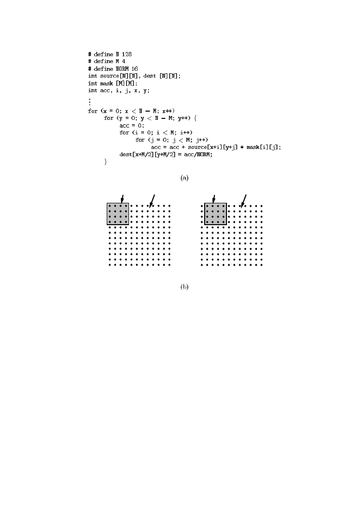
small mask array in the Scratch pad memory. This assignment eliminates
all conflicts in the data cache—the data cache is now used for memory
accesses to source, which are very regular. Storing mask on-chip ensures
that frequently accessed data is never ejected off-chip, thereby significantly
improving the memory performance and energy dissipation.
The Panda et al. [2000] memory assignment first determines the total
conflict factor (TCF) for each array, based on access frequency and possibi-
lity of conflict with other arrays, and then considers the arrays for
assignment to scratch pad memory in the order of TCF/(array size), giving
priority to high-conflict/small-size arrays.
A scratch-pad memory storing a small amount of frequently accessed
data on-chip has an equivalent in the instruction cache. The idea of using a
small buffer to store blocks of frequently used instructions was first
introduced in Jouppi [1990a]. Recent extensions of this strategy are the
decoded instruction buffer [Bajwa et al. 1997] and the L-cache [Bellas et al.
2000].
Mask Source
Mask Source
Iteration: x = 0, y = 0
Iteration: x = 0, y = 1
Fig. 17.
(a) Procedure CONV; (b) memory access pattern in CONV.
Data and Memory Optimization
•
187
ACM Transactions on Design Automation of Electronic Systems, Vol. 6, No. 2, April 2001.

3.7.5 Memory Architecture Exploration.
We now survey some recent
research that addresses the exploration sof cache memories. A number of
distinct memory architectures could be devised to efficiently exploit various
application-specific memory access patterns. Even if we restricted the scope
of the architecture to on-chip memory only, the various possible configura-
tions would be too large to explore, making it infeasible to exhaustively
simulate the performance and energy characteristics of an application for
each configuration. Thus, exploration tools are necessary to rapidly evalu-
ate the impact of several candidate architectures. Such tools can be of great
utility to a system designer by giving fast initial feedback on a wide range
of memory architectures [Panda et al. 1999b].
SRAM vs Data Cache.
Panda et al. [1999a] presented MemExplore, an
exploration framework for optimizing an on-chip data memory organiza-
tion, which addresses the following problem: given a certain amount of
on-chip memory space, partition it into data cache and scratch pad memory
so that total access time and energy dissipation are minimized, i.e., the
number of accesses to off-chip memory is minimized. In this formulation,
an on-chip memory architecture is defined as a combination of the total size
of on-chip memory used for data storage; the partitioning of this on-chip
memory into: scratch memory (characterized by its size) and data cache
(characterized by the cache size and the cache line size). For each candidate
of on-chip memory size
T, the technique divides T into cache (size C) and
scratch-pad memory (size
S
5 T 2 C), selecting only powers of 2 for C.
The procedure described in Section 3.7.4 is used to identify the right data
for storage in scratch-pad memory. Among the data assigned to be stored in
off-chip memory (and hence accessed through the cache), an estimate of
memory access performance is made by combining and analysis of the array
access patterns in the application and an approximate model of cache
behavior. The result of the estimate is the expected number of processor
cycles required for all memory accesses in the application. For each
T, the
~C, L! pair that is estimated to maximize performance is selected.
Example 13.
Typical exploration curves of the MemExplore algorithm
are shown in Figure 18. Figure 18(a) shows that the ideal division of a 2K
on-chip space is 1K in scratch-pad memory and 1K data cache. Figure 18(b)
shows that very little improvement in performance is observed beyond a
total on-chip memory size of 2KB.
The exploration curves of Figure 18 are generated from fast analytical
estimates, which are three orders of magnitude faster than actual simula-
tions, and are independent of data size. This estimation capability is
important in the initial stages of system design, where the number of
possible architectures is large, and a simulation of each architecture is
prohibitively expensive.
Performance vs Power.
The effects of cache size on performance and
cache power consumption was first studied by Kulkarni et al. [1998]. For a
188
•
P. R. Panda et al.
ACM Transactions on Design Automation of Electronic Systems, Vol. 6, No. 2, April 2001.
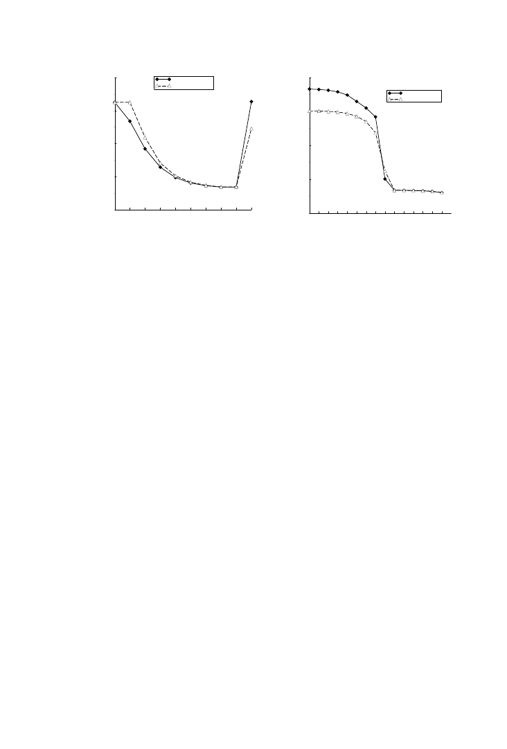
voice-coder application, it was shown that the performance was maximal
for cache sizes of 512 words or higher. However, the power of the memory-
related parts was minimal for128 words. This minimum was also clearly
influenced by other preceding code transformations such as the in-place
mapping approach. Without the in-place mapping, the minimum moved to
256 words. Shiue and Chakrabarti [1999] investigated this issue along
other axes, since they also examined the impact of the data layout tech-
nique in Section 3.7.1, the tiling/blocking optimization [Hennessy and
Patterson 1994], and set associativity on the data cache energy dissipation.
In their study of the MPEG decoder algorithm, they reported that the
minimum energy configuration of the implementation resulted from a
cache size of 64 bytes, whereas the minimum delay configuration occurred
at a size of 512 bytes. Both these studies provide important data for
energy-delay tradeoffs.
Datapath Width and Memory Size.
The CPU’s bit-width is an additional
parameter that can be tuned during architectural exploration of customiz-
able processors. Shackleford et al. [1997] studied the relationship between
the width of the processor data path and the memory subsystem. This
relationship is important when different data types with different sizes are
used in the application. The key observation is that as datapath width is
decreased, the data memory size decreases due to less wasted space. For
example, storing 3-bit data in a 4-bit word instead of an 8-bit word, but the
instruction memory might increase (e.g., storing 7-bit data in an 8-bit word
requires only one instruction to access it, but requires two instructions if a
4-bit datapath is used). The authors use RAM and ROM cost models to
evaluate the cost of candidate bit-widths in a combined CPU-memory
exploration.
Architectural
Description
Language-Driven
Processor/Memory
Co-
exploration.
Processor Architecture Description Languages (ADLs) were
developed to allow a language-driven exploration and software toolkit
4
8
16
32
64
128
256
512 1024 2048
Cache Size (Bytes)
200000
400000
600000
800000
1000000
Memor
y Cycles
Estimated Cycles
Actual Cycles
SRAM Size = 2048 Cache Size
4
8
16
32
64
128 256 512
1K
2K
4K
8K 16K 32K 64K
On-chip Memory Size (Bytes)
0
500000
1000000
1500000
2000000
Memor
y Cycles
Estimated Cycles
Actual Cycles
Fig. 18.
Histogram example. (a) Variation of memory performance with different mixes of
cache and scratch-pad memory for total on-chip memory of 2 KB; (b) variation of memory
performance with total on-chip memory space .
Data and Memory Optimization
•
189
ACM Transactions on Design Automation of Electronic Systems, Vol. 6, No. 2, April 2001.

generation approach [Tomiyama et al. 1999; Halambi et al. 1999b]. Cur-
rently, most ADLs assume an implicit/default memory organization, or are
limited to specifying the characteristics of a traditional memory hierarchy.
Since embedded systems may contain nontraditional memory organiza-
tions, there is a great need to explicitly model the memory subsystem for an
ADL-driven exploration approach. A recent approach [Mishra et al. 2001]
describes the use of EXPRESSION ADL [Halambi et al. 1999a] to drive the
exploration of memory architecture. The EXPRESSION ADL description of
the processor-memory architecture is used to explicitly capture the memory
architecture, including the characteristics of the memory modules (such as
caches, DRAMs, SRAMs DMAs), and the parallelism and pipelining in
memory architecture (e.g., resources used, timings, and access modes).
Each explicit memory architecture description is then used to automati-
cally generate the information needed by the compiler [Grun et al. 2000a;
2000b] to efficiently utilize features in the memory architecture and
generate a memory simulator, allowing feedback on the matches between
the application, the compiler, and the memory architecture to the designer.
In addition to the data cache research reviewed here, studies of the
instruction cache have also been reported [Kirovski et al. 1999; Li and
Henkel 1998; Li and Wolf 1999].
3.8 DRAM Optimizations
Applications involving large amounts of data typically need to store them
in off-chip DRAMs when the on-chip area does not afford sufficient storage.
The on-chip memory optimizations in the previous sections are not ade-
quate enough to efficiently handle the complex protocols associated with
DRAM memory. New abstractions are needed to model the various avail-
able memory access modes in order to effectively integrate the DRAM into
an automated synthesis system. This is especially important with the
advent of embedded DRAM technology, where it is possible to integrate
DRAM and logic into the same system on a chip [Panda et al. 1999b].
3.8.1 DRAM Modeling for HLS and Optimization.
The DRAM memory
address is split internally into a row address, consisting of the most
significant bits, and a column address, consisting of the least significant
bits. The row address selects a page from the core storage and the column
address selects an offset within the page to arrive at the desired word.
When an address is presented to the memory during a READ operation, the
entire page addressed by the row address is read into the page buffer, in
anticipation of spatial locality. If future accesses are to the same page, then
there is no need to access the main storage area because it can just be read
off the page buffer, which acts like a cache. Hence, subsequent accesses to
the same page are very fast.
Panda et al. [1998] describe a scheme for modeling the various memory
access modes and uses them to perform useful optimizations in the context
of an HLS environment.
190
•
P. R. Panda et al.
ACM Transactions on Design Automation of Electronic Systems, Vol. 6, No. 2, April 2001.

Example 14.
Figure 19(a) shows a simplified timing read cycle diagram
of a typical DRAM. The memory read cycle is initiated by the falling edge of
the RAS (row address strobe) signal, at which time the row address is
latched from the address bus. The column address is latched at the falling
edge of CAS (column address strobe) signal, which should occur at least
T
ras
5 45 ns later. Following this, the data is available on the data bus
after
T
cas
5 15 ns. Finally, the RAS signal is high for at least T
p
5 45 ns
to allow for bit-line precharge, which is necessary before the next memory
cycle can be initiated. In order to use the above information in an auto-
mated scheduling tool, we need to abstract a set of control data flow graph
(CDFG) nodes from the timing diagram [Panda et al. 1998]. For the
memory read operation, the CDFG node cluster consists of three stages
(Figure l9(b)): (1) row decode; (2) column decode; and (3) precharge. The
row and column addresses are available at the first and second stages,
respectively, and the output data is available at the beginning of the third
stage. Assuming a clock cycle of 15 ns, and a 1-cycle delay for the addition
and shift operations, we can derive the schedule in Figure 19(d) for the code
in Figure 19(c) using the memory read model in Figure 19(b). Since the four
accesses to array b are treated as four independent memory reads, each
incurs the entire read cycle delay of
T
rc
5 105 ns, i.e., 7 cycles, requiring a
total of
7
3 4 5 28 cycles.
However, DRAM features such as page mode read can be exploited
efficiently to generate a much tighter schedule for behaviors such as the
FindAverage example, which accesses data in the same page in succession.
Figure 19(e) shows the timing diagram for the page mode read cycle, and
Figure 19(f) shows the schedule for the FindAverage routine using the page
mode read feature. Note that the page mode does not incur the long row
decode and precharge times between successive accesses, thereby eliminat-
ing a significant amount of delay from the schedule. In this case, the
column decode time is followed by a minimum pulse width duration for the
CAS signal, which is also 15 ns in our example. Thus, the effective cycle
times between successive memory accesses was greatly reduced, resulting
in an overall reduction of 50% in the total schedule length.
The key feature in reducing the schedule length in the example above is
the recognition that input behavior is characterized by memory access
patterns amenable to the page mode feature and the incorporation of this
observation in the scheduling phase. Some additional DRAM-specific opti-
mizations discussed in Panda et al. [1998] are as follows:
Read-Modify-Write (R-M-W) optimization that takes advantage of the
R-M-W mode in modern DRAMs, which provides support for a more
efficient realization of the common case where a specific address is read,
the data is involved in a computation, and the output is written back to
the same location;
hoisting where the row-decode node is scheduled ahead of a conditional
node if the first memory access in both branches is on the same page;
Data and Memory Optimization
•
191
ACM Transactions on Design Automation of Electronic Systems, Vol. 6, No. 2, April 2001.
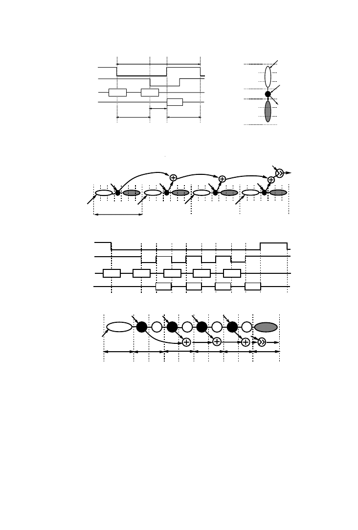
unrolling optimization in the context of supporting the page mode
accesses indicated in Figure 19(f).
The models described here can be introduced as I/O profiles in the memory
access ordering (SCBD) approach of Section 5. A good overview of the
Row
Addr
Data
Col
Addr
Stage 1:
RowDecode
(45ns)
Stage 3:
Precharge
(45 ns)
Stage 2:
ColDecode (15 ns)
(b)
Trc = 105 ns
RAS
CAS
Address
Data
Tcas = 15 ns
Tras = 45 ns
ROW
COL
VALID
Tp = 45 ns
(a)
av = (b[0] + b[1] + b[2] + b[3]) / 4
FindAverage:
RAS
CAS
Data
ROW
COL
COL
COL
COL
Addr
VAL
VAL
VAL
VAL
Optimized Schedule: 3 + 2 x 4 + 3 = 14 cycles
Row (b[0])
Col (b[0])
Col (b[1]) Col (b[2])
Col (b[3])
av
RowDecode
3 cycles
2 cycles
2 cycles
2 cycles
2 cycles Precharge
3 cycles
2
Unoptimized Schedule: 7 x 4 = 28 cycles
Row (b[0])
Col (b[0])
Row (b[1])
Col (b[1])
Row (b[2])
Col (b[2])
Row (b[3])
Col (b[3])
av
7 cycles
2
(c)
(e)
(f)
(d)
Fig. 19.
(a) Timing diagram for the memory read cycle; (b) model for memory read operation;
(c) code for FindAverage; (d) treating memory accesses as independent reads; (e) timing
diagram of the page mode read cycle; (f) treating memory accesses as a one-page mode read
cycle.
192
•
P. R. Panda et al.
ACM Transactions on Design Automation of Electronic Systems, Vol. 6, No. 2, April 2001.

performance implications of the architectural features in modern DRAMs is
found in Cuppu et al. [1999].
3.8.2 Synchronous DRAM/Banking Optimization.
As DRAM architec-
tures evolve, new challenges to the automatic synthesis of embedded
systems based on these memories appear. Synchronous DRAM represents
an architectural advance that presents another optimization opportunity:
multiple memory banks. The core memory storage is divided into multiple
banks, each with its own independent page buffer, so that two separate
memory pages can be simultaneously active in the multiple page buffers.
Khare et al. [1999] addressed the problem of modeling the access modes
of synchronous DRAMs such as:
burst mode read/write: fast successive accesses to data in the same page;
interleaved row read/write modes: alternating burst accesses between
banks;
interleaved column access: alternating burst accesses between two chosen
rows in different banks.
Memory bank assignment is performed by creating an interference graph
between arrays and partitioning it into subgraphs so that data in each part
is assigned to a different memory bank. The bank assignment algorithm is
related to techniques such as those of Sudarsanam and Malik [2000] that
address memory assignment for DSP processors like the Motorola 56000,
which has a dual-bank internal memory/register file [Saghir et al. 1996;
Cruz et al. 2000]. The bank assignment problem in Sudarsanam and Malik
[2000] is targeted at scalar variables, and is solved in conjunction with
register allocation by building a constraint graph that models the data
transfer possibilities between registers and memories followed by a simu-
lated annealing step.
Chang and Lin [2000] approached the SDRAM bank assignment problem
by first constructing an array distance table. This table stores the distance
in the DFG between each pair of arrays in the specification. A short
distance indicates a strong correlation—for instance, that they may possi-
bly be two inputs of the same operation, and hence would benefit from
being assigned to separate banks. The bank assignment is finally per-
formed by considering array pairs in increasing order of their array
distance information.
The presence of embedded DRAMs adds several new dimensions to
traditional architecture exploration. One interesting aspect of DRAM archi-
tecture that can be customized for an application is the banking structure.
Figure 20(a) illustrates a common problem with the single-bank DRAM
architecture. If we have a loop that in succession accesses data from three
large arrays A, B, and C, each of which is much larger than a page, then
each memory access leads to a fresh page being read from the storage,
effectively cancelling the benefits of the page buffer. This page buffer
interference problem cannot be avoided if a fixed architecture DRAM is
Data and Memory Optimization
•
193
ACM Transactions on Design Automation of Electronic Systems, Vol. 6, No. 2, April 2001.
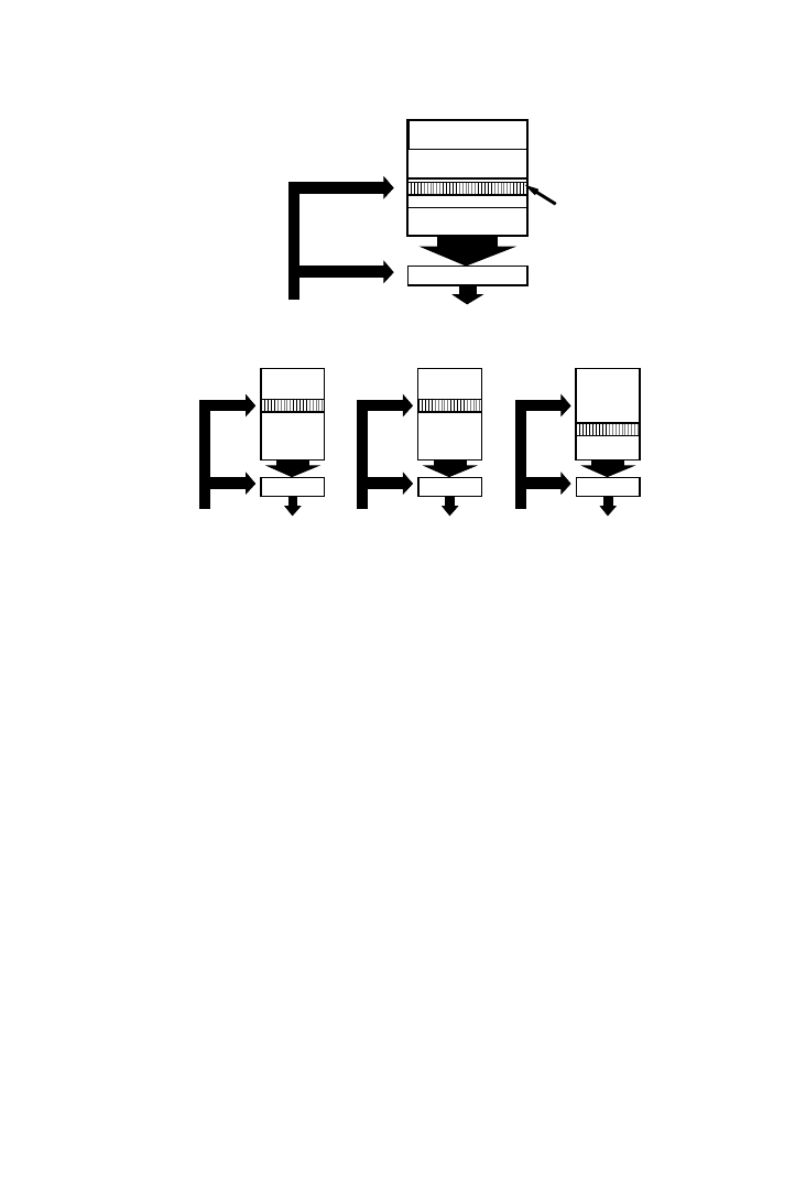
used. However, an elegant solution to the problem is available if the
banking configuration of the DRAM can be customized for the application
[Panda 1999]. Thus, in the example in Figure 20, the arrays can be
assigned to separate banks as shown in Figure 20(b). Since each bank has
its own private page buffer, there is no interference between the arrays and
the memory accesses do not represent a bottleneck.
In order to customize the banking structure for an application, we need
to solve the memory bank assignment problem— determine an optimal
banking structure (number of banks) and the assignment of each array
variable into the banks such that the number of page misses is minimized.
This objective optimizes both the performance and the energy dissipation of
the memory subsystem. The memory bank customization problem is solved
in Panda [1999] by modeling the assignment as a partitioning problem, i.e.,
partition a given set of nodes into a given number of groups such that a
given criterion (bank misses in this case) is optimized. The partitioning
proceeds by associating a cost of assigning two arrays into the same bank,
determined by the number of accesses to the arrays and the loop count. If
the arrays are accessed in the same loop, then the cost is high, thereby
discouraging the partitioning algorithm from assigning them to the same
bank. On the other hand, if two arrays are never accessed in the same loop,
then they are candidates for assignment into the same bank. This pairing
(a)
Page Buffer
Addr [15:0]
Row Address
Addr [15:8]
Col Address
Addr [7:0]
To Datapath
A
Page
To Datapath
Row
Col
Buffer
Addr
B[i]
To Datapath
Row
Col
Buffer
Addr
C[2i]
To Datapath
Row
Col
Buffer
Addr
A[i]
(b)
B
C
Fig. 20.
(a) Arrays mapped to a single-bank memory; (b) 3– bank memory architecture.
194
•
P. R. Panda et al.
ACM Transactions on Design Automation of Electronic Systems, Vol. 6, No. 2, April 2001.

is associated with a low cost, guiding the partitioner to assign the arrays
together.
Bank assignment can also be seen as the array-to-memory assignment in
Section 3.2, when the appropriate cost function and I/O profile constraints
are introduced [Brockmeyer et al. 2000a].
3.8.3 Memory-Aware
Compilation.
Traditionally,
the
compiler
is
shielded from the detailed organization and timing of the memory sub-
system; interactions with the memory subsystem are typically through read
and write operations with timing granularity at the level of cache hit and
miss delays. However, a memory-aware compiler approach can aggressively
exploit the detailed timing information of the memory subsystem to obtain
improved scheduling results. Grun et al. [2000a] present an algorithm,
called TIMGEN, to include DRAM characteristics in a compiler framework.
Detailed timing information on DRAM nodes is made available to the
compiler, which can then make intelligent scheduling decisions based on
timing knowledge. For each instruction, TIMGEN traces a detailed timing
path through the processor pipeline, including different possible memory
access modes. This information is then used during scheduling to generate
aggressive schedules that are on the average 24% smaller than one that
assumes no knowledge of memory timing.
4. ADDRESS GENERATION
One important consequence of all the above memory organization-related
steps, is that the address sequences typically become much more compli-
cated than in the original nonoptimized application code. This is first of all
due to the source code transformations like in-place mapping that intro-
duce modulo arithmetic and loop transformations, which in turn generate
more index arithmetic and manifest local conditions. Additional complexity
is added by the very distributed memory organization used in embedded
processors, both custom and programmable. As a result, address genera-
tion, which involves generating efficient assembly code or hardware to
implement the translation of array references to actual memory addresses,
is a critical stage in the entire data management flow.
Initial work on address generation focused only on regular DSP applica-
tions mapped on hardware. Central to this early research is the observation
that if the generated addresses were known to be periodic (true for many
DSP applications accessing large data arrays), then there would be no need
to use a full-blown arithmetic circuit to generate the sequence; a simple
counter-based circuit could achieve the same effect. Initial research on
synthesizing hardware address generation focused on generating efficient
designs from a specified trace of memory address [Grant et al. 1989; Grant
and Denyer 1991] by recognizing the periodicity of the patterns and
automatically building a counter-based circuit for generating the sequence
of addresses. Since the problem of extracting the periodic behavior from an
arbitrary sequence of addresses can be extremely difficult, work like that of
Grant and Denyer [1991] relies on designer hints such as number of
Data and Memory Optimization
•
195
ACM Transactions on Design Automation of Electronic Systems, Vol. 6, No. 2, April 2001.

memory accesses in the basic repeating pattern. The ZIPPO system [Grant
et al. 1994] solves a generalization of the above problem by considering
several address streams that are incident on different memory modules
on-chip, and synthesizing an address generator that is optimized by shar-
ing hardware. Multiplexing such sequences allows more exploratory free-
dom and produces better results [Miranda et al. 1994].
Another simplification of address generation hardware can be achieved
by employing certain interesting properties of the exclusive OR (XOR)
function. Schmit and Thomas [1998] presented an address bit inversion
technique for generating a simplified address generator at the expense of a
small area overhead. The authors point out that if two arrays
a and b have
sizes
0... A
2 1 and 0...B 2 1, respectively, such that A&B 5 0, i.e., the
bitwise AND of the arrays sizes is zero, then two disjoint address spaces
are created by performing a bitwise XOR on the index of one array with the
size of the other.
Example 15.
Suppose we have to store two arrays
a and b with sizes of
3 and 4 words, respectively, in the same memory module. In order to access
random elements
a
@i# and b@ j # from memory, the arrays would normally
be located contiguously in memory, and the addressing circuit would be
implemented as follows:
Address for a[i]: i
Address for b[j]: 3
1
j
However, since the bitwise AND of 3 and 4 is zero, we can use the
following implementation to generate distinct memory address spaces for
a
and
b.
Address for a[i]: i XOR 4
Address for b[j]: j XOR 3
The latter addressing scheme is asymptotically faster because it incurs a
maximum of one inverter delay, whereas the former incurs the delay due to
an adder circuit. The disadvantage of the address bit inversion technique is
that the array sizes have to be increased until the condition
A&B
5 0 is
satisfied. This involves wasting memory space, which is a maximum of
17.4% in the author’s experiments.
An alternative approach to the above was proposed by Miranda et al.
[1998] where custom architectures based on arithmetic building blocks
(application-specific units – ASUs) are explored. In this context, time
multiplexing and merging of index expressions were crucial in obtaining a
cost-efficient result. Easily computable measures could be estimated from
the application code in deciding whether the counter-based or ASU-based
approaches worked best, on the basis of individual address expressions.
The combined Adopt methodology for address generation described in-
Miranda et al. [1998] is a general framework for optimizing address
generators. First, an address expression extraction step obtains the address
expressions from the internal control/data flow graph representation. Next,
196
•
P. R. Panda et al.
ACM Transactions on Design Automation of Electronic Systems, Vol. 6, No. 2, April 2001.

address expression splitting and clustering leads to several optimization
opportunities while selecting the target architecture, which can be one of
two types: an incremental address generation unit and a custom address
calculation unit. Algebraic transformations are finally applied to globally
optimize the generated addressing logic.
In addition to these custom address generation approaches, much effort
was also spent on mapping application code on programmable address
generators. Examples of early work exploiting auto-increment modes and
dealing with limitations on (index) register storage are Leupers and Mar-
wedel [1996] and Liem et al. [1996]. Additional optimization steps were
introduced later to support algebraic factoring and polynomial induction
variable analysis [Gupta et al. 2000] and modulo arithmetic [Ghez et al.
2000].
5. CONCLUSIONS
We have presented a survey of contemporary and emerging data and
memory optimization techniques for embedded systems.
We first discussed platform-independent memory optimizations that op-
erate on a source-to-source level, and typically guarantee improved perfor-
mance, power, and cost metrics, irrespective of the implementation’s target
architecture. Next, we surveyed a number of data and memory optimization
techniques applicable to memory structures at different levels of architec-
tural granularity: from registers and register files, all the way up to
off-chip memory structures. Finally, we discussed the attendant address
generation optimizations that remove the address and local control over-
head that appears as a byproduct of both platform-independent, as well as
platform-dependent, data and memory optimizations.
Given the constraints on the length of this manuscript, we have at-
tempted to survey a wide range of both traditional approaches as well as
emerging techniques designed to handle memory issues in embedded
systems, from the viewpoint of performance, power, and area (cost). We
have not addressed the contexts of many parallel platforms including data-
and (dynamic) task-level parallelism. Many open issues remain in the
context of memory-intensive embedded systems, including testing, valida-
tion, and (formal) verification, embedded system reliability, and optimiza-
tion opportunities in the context of networked embedded systems.
As complex embedded systems-on-a-chip (SOC) begin to proliferate, and
as the software content of these embedded SOCs dominate the design
process, memory issues will continue to be a critical optimization dimen-
sion in the design and development of future embedded systems.
ACKNOWLEDGMENTS
We gratefully acknowledge the input from our colleagues at IMEC and the
ACES laboratory at U.C. Irvine and their many research contributions,
which are partly summarized in this survey.
Data and Memory Optimization
•
197
ACM Transactions on Design Automation of Electronic Systems, Vol. 6, No. 2, April 2001.

REFERENCES
A
GARWAL
, A., K
RANTZ
, D.,
AND
N
ATARANJAN
, V. 1995. Automatic partitioning of parallel loops
and data arrays for distributed shared-memory multiprocessors.
IEEE Trans. Parallel
Distrib. Syst. 6, 9 (Sept.), 943–962.
A
HMAD
, I.
AND
C
HEN
, C. Y. R. 1991. Post-processor for data path synthesis using multiport
memories. In Proceedings of the IEEE/ACM International Conference on Computer-Aided
Design (ICCAD ’91, Santa Clara, CA, Nov. 11-14).
IEEE Computer Society Press, Los
Alamitos, CA, 276 –279.
A
HO
, A., S
ETHI
, R.,
AND
U
LLMAN
, J.
1986.
Compilers: Principles, Techniques, and
Tools. Addison-Wesley, Reading, MA.
A
MARASINGHE
, S., A
NDERSON
, J., L
AM
, M.,
AND
T
SENG
, C.-W. 1995. An overview of the suif
compiler for scalable parallel machines. In Proceedings of the SIAM Conference on Parallel
Processing for Scientific Computing (San Francisco, CA, Feb.). SIAM, Philadelphia, PA.
B
AJWA
, R. S., H
IRAKI
, M., K
OJIMA
, H., G
ORNY
, D. J., N
ITTA
, K., S
HRIDHAR
, A., S
EKI
, K.,
AND
S
ASAKI
, K.
1997.
Instruction buffering to reduce power in processors for signal
processing. IEEE Trans. Very Large Scale Integr. Syst. 5, 4, 417– 424.
B
AKSHI
, S.
AND
G
AJSKI
, D. D.
1995.
A memory selection algorithm for high-performance
pipelines. In Proceedings of the European Conference EURO-DAC ’95 with EURO-VHDL ’95
on Design Automation (Brighton, UK, Sept. 18 –22), G. Musgrave, Ed.
IEEE Computer
Society Press, Los Alamitos, CA, 124 –129.
B
ALAKRISHNAN
, M., B
ANERJI
, D. K., M
AJUMDAR
, A. K., L
INDERS
, J. G.,
AND
M
AJITHIA
, J.
C. 1990. Allocation of multiport memories in data path synthesis. IEEE Trans. Comput.-
Aided Des. 7, 4 (Apr.), 536 –540.
B
ALASA
, F., C
ATTHOOR
, F.,
AND
D
E
M
AN
, H.
1994.
Dataflow-driven memory allocation for
multi-dimensional signal processing systems.
In Proceedings of the 1994 IEEE/ACM
International Conference on Computer-Aided Design (ICCAD ’94, San Jose, CA, Nov. 6 –10),
J. A. G. Jess and R. Rudell, Eds. IEEE Computer Society Press, Los Alamitos, CA, 31–34.
B
ALASA
, F., C
ATTHOOR
, F.,
AND
D
E
M
AN
, H. 1995. Background memory area estimation for
multidimensional signal processing systems. IEEE Trans. Very Large Scale Integr. Syst. 3,
2 (June), 157–172.
B
ANERJEE
, P., C
HANDY
, J., G
UPTA
, M., H
ODGES
, E., H
OLM
, J., L
AIN
, A., P
ALERMO
, D., R
A
-
MASWAMY
, S.,
AND
S
U
, E.
1995.
The paradigm compiler for distributed-memory
multicomputers. IEEE Computer 28, 10 (Oct.), 37– 47.
B
ANERJEE
, U. 1998. Dependence Analysis for Supercomputing. Kluwer Academic Publishers,
Hingham, MA.
B
ANERJEE
, U., E
IGENMANN
, R., N
ICOLAU
, A.,
AND
P
ADUA
, D. A.
1993.
Automatic program
parallelization. Proc. IEEE 81, 2 (Feb.), 211–243.
B
ELLAS
, N., H
AJJ
, I. N., P
OLYCHRONOPOULOS
, C. D.,
AND
S
TAMOULIS
, G. 2000. Architectural and
compiler techniques for energy reduction in high-performance microprocessors.
IEEE
Trans. Very Large Scale Integr. Syst. 8, 3 (June), 317–326.
B
ENINI
, L.
AND DE
M
ICHELI
, G.
2000.
System-level power optimization techniques and
tools. ACM Trans. Des. Autom. Electron. Syst. 5, 2 (Apr.), 115–192.
B
ENINI
, L., D
E
M
ICHELI
, G., M
ACII
, E., P
ONCINO
, M.,
AND
Q
UER
, S. 1998a. Power optimization
of core-based systems by address bus encoding. IEEE Trans. Very Large Scale Integr. Syst.
6, 4, 554 –562.
B
ENINI
, L., D
E
M
ICHELI
, G., M
ACII
, E., S
CIUTO
, D.,
AND
S
ILVANO
, C.
1998b.
Address bus
encoding techniques for system-level power optimization. In Proceedings of the Conference
on Design, Automation and Test in Europe 98. 861– 866.
B
ENINI
, L., M
ACII
, A.,
AND
P
ONCINO
, M. 2000. A recursive algorithm for low-power memory
partitioning. In Proceedings of the IEEE International Symposium on Low Power Design
(Rapallo, Italy, Aug.). IEEE Computer Society Press, Los Alamitos, CA, 78 – 83.
B
ROCKMEYER
, E., V
ANDECAPPELLE
, A.,
AND
C
ATTHOOR
, F.
2000a.
Systematic cycle budget
versus system power trade-off: a new perspective on system exploration of real-time data-
dominated applications. In Proceedings of the IEEE International Symposium on Low Power
Design (Rapallo, Italy, Aug.). IEEE Computer Society Press, Los Alamitos, CA, 137–142.
198
•
P. R. Panda et al.
ACM Transactions on Design Automation of Electronic Systems, Vol. 6, No. 2, April 2001.

B
ROCKMEYER
, E., W
UYTACK
, S., V
ANDECAPPELLE
, A.,
AND
C
ATTHOOR
, F.
2000b.
Low power
storage cycle budget tool support for hierarchical graphs.
In Proceedings of the 13th
ACM/IEEE International Symposium on System-Level Synthesis (Madrid, Sept).
ACM
Press, New York, NY, 20 –22.
C
ATTHOOR
, F., D
ANCKAERT
, K., K
ULKARNI
, C.,
AND
O
MNES
, T. 2000. Data transfer and storage
architecture issues and exploration in multimedia processors.
In Programmable Digital
Signal Processors: Architecture, Programming, and Applications, Y. H. Yu, Ed.
Marcel
Dekker, Inc., New York, NY.
C
ATTHOOR
, F., J
ANSSEN
, M., N
ACHTERGAELE
, L.,
AND
M
AN
, H. D. 1996. System-level data-flow
transformations for power reduction in image and video processing. In Proceedings of the
International Conference on Electronic Circuits and Systems on Electronic Circuits and
Systems (Oct.). 1025–1028.
C
ATTHOOR
, F., W
UYTACK
, S., D
E
G
REEF
, E., B
ALASA
, F., N
ACHTERGAELE
, L.,
AND
V
ANDECAPPELLE
,
A. 1998. Custom Memory Management Methodology: Exploration of Memory Organization
for Embedded Multimedia System Design. Kluwer Academic, Dordrecht, Netherlands.
C
ATTHOOR
, F., F
RANSSEN
, F., W
UYTACK
, S., N
ACHTERGAELE
, L.,
AND
D
E
M
AN
, H. 1994. Global
communication and memory optimizing transformations for low power systems. In Proceed-
ings of the International Workshop on Low Power Design. 203–208.
C
HAITIN
, G., A
USLANDER
, M., C
HANDRA
, A., C
OCKE
, J., H
OPKINS
, M.,
AND
M
ARKSTEIN
,
P. 1981. Register allocation via coloring. Comput. Lang. 6, 1, 47–57.
C
HANG
, H.-K
AND
L
IN
, Y.-L.
2000.
Array allocation taking into account SDRAM
characteristics.
In Proceedings of the Asia and South Pacific Conference on Design
Automation (Yokohama, Jan.). 497–502.
C
HEN
, T.-S.
AND
S
HEU
, J.-P.
1994.
Communication-free data allocation techniques for
parallelizing compilers on multicomputers. IEEE Trans. Parallel Distrib. Syst. 5, 9 (Sept.),
924 –938.
C
IERNIAK
, M.
AND
L
I
, W.
1995.
Unifying data and control transformations for distributed
shared-memory machines. SIGPLAN Not. 30, 6 (June), 205–217.
C
RUZ
, J.-L., G
ONZALEZ
, A., V
ALERO
, M.,
AND
T
OPHAM
, N. 2000. Multiple-banked register file
architectures. In Proceedings of the 27th International Symposium on Computer Architec-
ture (ISCA-27, Vancouver, B.C., June). ACM, New York, NY, 315–325.
C
UPPU
, V., J
ACOB
, B. L., D
AVIS
, B.,
AND
M
UDGE
, T. N. 1999. A performance comparison of
contemporary dram architectures.
In Proceedings of the International Symposium on
Computer Architecture (Atlanta, GA, May). 222–233.
DA
S
ILVA
, J. L., C
ATTHOOR
, F., V
ERKEST
, D.,
AND DE
M
AN
, H.
1998.
Power exploration for
dynamic data types through virtual memory management refinement. In Proceedings of the
1998 International Symposium on Low Power Electronics and Design (ISLPED ’98,
Monterey, CA, Aug. 10 –12), A. Chandrakasan and S. Kiaei, Chairs. ACM Press, New York,
NY, 311–316.
D
ANCKAERT
, K., C
ATTHOOR
, F.,
AND
M
AN
, H. D. 1996. System-level memory management for
weakly parallel image processing. In Proceedings of the Conference on EuroPar’96 Parallel
Processing (Lyon, France, Aug.). Springer-Verlag, New York, NY, 217–225.
D
ANCKAERT
, K., C
ATTHOOR
, F.,
AND
M
AN
, H. D. 1999. Platform independent data transfer and
storage exploration illustrated on a parallel cavity detection algorithm. In Proceedings of
the International Conference on Parallel and Distributed Processing Techniques and Appli-
cations (PDPTA99). 1669 –1675.
D
ANCKAERT
, K., C
ATTHOOR
, F.,
AND
M
AN
, H. D. 2000. A preprocessing step for global loop
transformations for data transfer and storage optimization. In Proceedings of the Interna-
tional Conference on Compilers, Architecture and Synthesis for Embedded Systems (San Jose
CA, Nov.).
D
ARTE
, A., R
ISSET
, T.,
AND
R
OBERT
, Y. 1993. Loop nest scheduling and transformations. In
Environments and Tools for Parallel Scientific Computing, J. J. Dongarra and B. Tou-
rancheau, Eds. Elsevier Advances in parallel computing series. Elsevier Sci. Pub. B. V.,
Amsterdam, The Netherlands, 309 –332.
D
ARTE
, A.
AND
R
OBERT
, Y. 1995. Affine-by-statement scheduling of uniform and affine loop
nests over parametric domains. J. Parallel Distrib. Comput. 29, 1 (Aug. 15), 43–59.
Data and Memory Optimization
•
199
ACM Transactions on Design Automation of Electronic Systems, Vol. 6, No. 2, April 2001.

D
IGUET
, J. P
H
., W
UYTACK
, S., C
ATTHOOR
, F.,
AND
D
E
M
AN
, H. 1997. Formalized methodology
for data reuse exploration in hierarchical memory mappings. In Proceedings of the 1997
International Symposium on Low Power Electronics and Design (ISLPED ’97, Monterey, CA,
Aug. 18 –20), B. Barton, M. Pedram, A. Chandrakasan, and S. Kiaei, Chairs. ACM Press,
New York, NY, 30 –35.
D
ING
, C.
AND
K
ENNEDY
, K. 2000. The memory bandwidth bottleneck and its amelioration by a
compiler.
In Proceedings of the International Symposium on Parallel and Distributed
Processing (Cancun, Mexico, May). 181–189.
D
E
G
REEF
, E.
AND
C
ATTHOOR
, F.
1996.
Reducing storage size for static control programs
mapped onto parallel architectures.
In Proceedings of the Dagstuhl Seminar on Loop
Parallelisation (Schloss Dagstuhl, Germany, Apr.).
F
EAUTRIER
, P.
1991.
Dataflow analysis of array and scalar references.
Int. J. Parallel
Program. 20, 1, 23–53.
F
EAUTRIER
,
P.
1995.
Compiling
for
massively
parallel
architectures:
A
perspective. Microprocess. Microprogram. 41, 5-6 (Oct.), 425– 439.
F
RABOULET
, A., H
UARD
, G.,
AND
M
IGNOTTE
, A.
1999.
Loop alignment for memory access
optimisation. In Proceedings of the 12th ACM/IEEE International Symposium on System-
Level Synthesis (San Jose CA, Dec.). ACM Press, New York, NY, 70 –71.
F
RANSSEN
, F., B
ALASA
, F.,
VAN
S
WAAIJ
, M., C
ATTHOOR
, F.,
AND
M
AN
, H. D. 1993. Modeling
multi-dimensional data and control flow. IEEE Trans. Very Large Scale Integr. Syst. 1, 3
(Sept.), 319 –327.
F
RANSSEN
, F., N
ACHTERGAELE
, L., S
AMSOM
, H., C
ATTHOOR
, F.,
AND
M
AN
, H. D. 1994. Control
flow optimization for fast system simulation and storage minimization. In Proceedings of
the International Conference on Design and Test (Paris, Feb.). 20 –24.
G
AJSKI
, D., D
UTT
, N., L
IN
, S.,
AND
W
U
, A. 1992. High Level Synthesis: Introduction to Chip
and System Design. Kluwer Academic Publishers, Hingham, MA.
G
AREY
, M. R.
AND
J
OHNSON
, D. S. 1979. Computers and Intractibility – A Guide to the Theory
of NP-Completeness. W. H. Freeman and Co., New York, NY.
G
HEZ
, C., M
IRANDA
, M., V
ANDECAPPELLE
, A., C
ATTHOOR
, F.,
AND
V
ERKEST
, D. 2000. Systematic
high-level address code transformations for piece-wise linear indexing: illustration on a
medical imaging algorithm.
In Proceedings of the IEEE Workshop on Signal Processing
Systems (Lafayette, LA, Oct.). IEEE Press, Piscataway, NJ, 623– 632.
G
ONZÁLEZ
, A., A
LIAGAS
, C.,
AND
V
ALERO
, M.
1995.
A data cache with multiple caching
strategies tuned to different types of locality. In Proceedings of the 9th ACM International
Conference on Supercomputing (ICS ’95, Barcelona, Spain, July 3–7), M. Valero,
Chair. ACM Press, New York, NY, 338 –347.
G
OOSSENS
, G., V
ANDEWLLE
, J.,
AND
D
E
M
AN
, H. 1989. Loop optimization in register-transfer
scheduling for DSP-systems. In Proceedings of the 26th ACM/IEEE Conference on Design
Automation (DAC ’89, Las Vegas, NV, June 25-29), D. E. Thomas, Ed. ACM Press, New
York, NY, 826 – 831.
G
RANT
, D.
AND
D
ENYER
, P. B. 1991. Address generation for array access based on modulus m
counters.
In Proceedings of the European Conference on Design Automation (EDAC,
Feb.). 118 –123.
G
RANT
, D., D
ENYER
, P. B.,
AND
F
INLAY
, I.
1989.
Synthesis of address generators.
In
Proceedings of the IEEE/ACM International Conference on Computer-Aided Design (ICCAD
’89, Santa Clara, CA, Nov.). ACM Press, New York, NY, 116 –119.
G
RANT
, D. M., M
EERBERGEN
, J. V.,
AND
L
IPPENS
, P. E. R.
1994.
Optimization of address
generator hardware. In Proceedings of the 1994 Conference on European Design and Test
(Paris, France, Feb.). 325–329.
G
REEF
, E. D., C
ATTHOOR
, F.,
AND
M
AN
, H. D. 1995. Memory organization for video algorithms
on programmable signal processors. In Proceedings of the IEEE International Conference on
Computer Design (ICCD ’95, Austin TX, Oct.). IEEE Computer Society Press, Los Alamitos,
CA, 552–557.
G
REEF
, E. D., C
ATTHOOR
, F.,
AND
M
AN
, H. D. 1997. Array placement for storage size reduction
in embedded multimedia systems.
In Proceedings of the International Conference on
Applic.-Spec./Array Processors (Zurich, July). 66 –75.
200
•
P. R. Panda et al.
ACM Transactions on Design Automation of Electronic Systems, Vol. 6, No. 2, April 2001.

G
RUN
, P., B
ALASA
, F.,
AND
D
UTT
, N.
1998.
Memory size estimation for multimedia
applications. In Proceedings of the Sixth International Workshop on Hardware/Software
Codesign (CODES/CASHE ’98, Seattle, WA, Mar. 15–18), G. Borriello, A. A. Jerraya, and L.
Lavagno, Chairs. IEEE Computer Society Press, Los Alamitos, CA, 145–149.
G
RUN
, P., D
UTT
, N.,
AND
N
ICOLAU
, A. 2000a. Memory aware compilation through accurate
timing extraction. In Proceedings of the Conference on Design Automation (Los Angeles, CA,
June). ACM Press, New York, NY, 316 –321.
G
RUN
, P., D
UTT
, N.,
AND
N
ICOLAU
, A. 2000b. MIST: An algorithm for memory miss traffic
management.
In Proceedings of the IEEE/ACM International Conference on Computer-
Aided Design (San Jose, CA, Nov.). ACM Press, New York, NY, 431– 437.
G
RUN
, P., D
UTT
, N.,
AND
N
ICOLAU
, A. 2001. Access pattern based local memory customization
for low power embedded systems. In Proceedings of the Conference on Design, Automation,
and Test in Europe (Munich, Mar.).
G
UPTA
, M., S
CHONBERG
, E.,
AND
S
RINIVASAN
, H.
1996.
A unified framework for optimizing
communication in data-parallel programs.
IEEE Trans. Parallel Distrib. Syst. 7, 7,
689 –704.
G
UPTA
, S., M
IRANDA
, M., C
ATTHOOR
, F.,
AND
G
UPTA
, R. 2000. Analysis of high-level address
code transformations for programmable processors. In Proceedings of the 3rd ACM/IEEE
Conference on Design and Test in Europe (Mar.). ACM Press, New York, NY, 9 –13.
H
ALAMBI
, A., G
RUN
, P., G
ANESH
, V., K
HARE
, A., D
UTT
, N.,
AND
N
ICOLAU
, A. 1999a. Expression:
A language for architecture exploration through compiler/simulator retargetability.
In
Proceedings of the Conference on DATE (Munich, Mar.).
H
ALAMBI
, A., G
RUN
, P., T
OMIYAMA
, H., D
UTT
, N.,
AND
N
ICOLAU
, A. 1999b. Automatic software
toolkit generation for embedded systems-on-chip. In Proceedings of the Conference on ICVC.
H
ALL
, M. W., H
ARVEY
, T. J., K
ENNEDY
, K., M
C
I
NTOSH
, N., M
C
K
INLEY
, K. S., O
LDHAM
, J. D.,
P
ALECZNY
, M. H.,
AND
R
OTH
, G.
1993.
Experiences using the ParaScope Editor: an
interactive parallel programming tool. SIGPLAN Not. 28, 7 (July), 33– 43.
H
ALL
, M., A
NDERSON
, J., A
MARASINGHE
, S., M
URPHY
, B., L
IAO
, S., B
UGNION
, E.,
AND
L
AM
, M.
1996. Maximizing multiprocessor performance with the SUIF compiler. IEEE Computer 29,
12 (Dec.), 84 – 89.
H
ENNESSY
, J. L.
AND
P
ATTERSON
, D. A.
1996.
Computer Architecture: A Quantitative
Approach. 2nd ed. Morgan Kaufmann Publishers Inc., San Francisco, CA.
H
UANG
, C.-Y., C
HEN
, Y.-S., L
IN
, Y.-L.,
AND
H
SU
, Y.-C. 1990. Data path allocation based on
bipartite weighted matching. In Proceedings of the 27th ACM/IEEE Conference on Design
Automation (DAC ’90, Orlando, FL, June 24-28), R. C. Smith, Chair. ACM Press, New York,
NY, 499 –504.
ISO/IEC M
OVING
P
ICTURE
E
XPERTS
G
ROUP
. 2001. The MPEG Home Page (http://www.cselt.it/
mpeg/)
11.
I
TOH
, K., S
ASAKI
, K.,
AND
N
AKAGOME
, Y.
1995.
Trends in low-power RAM circuit
technologies. Proc. IEEE 83, 4 (Apr.), 524 –543.
J
HA
, P. K.
AND
D
UTT
, N.
1997.
Library mapping for memories.
In Proceedings of the
Conference on European Design and Test (Mar.). 288 –292.
J
OUPPI
, N.
1990.
Improving direct-mapped cache performance by the addition of a small
fully-associative cache and prefetch buffers.
In Proceedings of the 17th International
Symposium on Computer Architecture (ISCA ’90, Seattle, WA, May). IEEE Press, Piscat-
away, NJ, 364 –373.
K
ANDEMIR
, M., V
IJAYKRISHNAN
, N., I
RWIN
, M. J.,
AND
Y
E
, W.
2000.
Influence of compiler
optimisations on system power. In Proceedings of the Conference on Design Automation (Los
Angeles, CA, June). ACM Press, New York, NY, 304 –307.
K
ARCHMER
, D.
AND
R
OSE
, J. 1994. Definition and solution of the memory packing problem for
field-programmable systems. In Proceedings of the 1994 IEEE/ACM International Confer-
ence on Computer-Aided Design (ICCAD ’94, San Jose, CA, Nov. 6 –10), J. A. G. Jess and R.
Rudell, Eds. IEEE Computer Society Press, Los Alamitos, CA, 20 –26.
K
ELLY
, W.
AND
P
UGH
, W. 1992. Generating schedules and code within a unified reordering
transformation framework. UMIACS-TR-92-126. University of Maryland at College Park,
College Park, MD.
Data and Memory Optimization
•
201
ACM Transactions on Design Automation of Electronic Systems, Vol. 6, No. 2, April 2001.

K
HARE
, A., P
ANDA
, P. R., D
UTT
, N. D.,
AND
N
ICOLAU
, A.
1999.
High-level synthesis with
SDRAMs and RAMBUS DRAMs. IEICE Trans. Fundam. Electron. Commun. Comput. Sci.
E82-A, 11 (Nov.), 2347–2355.
K
IM
, T.
AND
L
IU
, C. L. 1993. Utilization of multiport memories in data path synthesis. In
Proceedings of the 30th ACM/IEEE International Conference on Design Automation (DAC
’93, Dallas, TX, June 14 –18), A. E. Dunlop, Ed. ACM Press, New York, NY, 298 –302.
K
IROVSKI
, D., L
EE
, C., P
OTKONJAK
, M.,
AND
M
ANGIONE
-S
MITH
, W.
1999.
Application-driven
synthesis of memory-intensive systems-on-chip.
IEEE Trans. Comput.-Aided Des. 18, 9
(Sept.), 1316 –1326.
K
JELDSBERG
, P. G., C
ATTHOOR
, F.,
AND
A
AS
, E. J. 2000a. Automated data dependency size
estimation with a partially fixed execution ordering.
In Proceedings of the IEEE/ACM
International Conference on Computer-Aided Design (San Jose, CA, Nov.). ACM Press, New
York, NY, 44 –50.
K
JELDSBERG
, P. G., C
ATTHOOR
,, F.,
AND
A
AS
, E. J. 2000b. Storage requirement estimation for
data-intensive applications with partially fixed execution ordering. In Proceedings of the
ACM/IEEE Workshop on Hardware/Software Co-Design (San Diego CA, May). ACM Press,
New York, NY, 56 – 60.
K
OHAVI
, Z. 1978. Switching and Finite Automata Theory. McGraw-Hill, Inc., New York, NY.
K
OLSON
, D. J., N
ICOLAU
, A.,
AND
D
UTT
, N. 1994. Minimization of memory traffic in high-level
synthesis. In Proceedings of the 31st Annual Conference on Design Automation (DAC ’94,
San Diego, CA, June 6 –10), M. Lorenzetti, Chair. ACM Press, New York, NY, 149 –154.
K
RAMER
, H.
AND
M
ULLER
, J. 1992. Assignment of global memory elements for multi-process
vhdl specifications.
In Proceedings of the International Conference on Computer Aided
Design. 496 –501.
K
ULKARNI
, C., C
ATTHOOR
, F.,
AND
M
AN
, H. D.
1999.
Cache transformations for low power
caching in embedded multimedia processors. In Proceedings of the International Sympo-
sium on Parallel Processing (Orlando, FL, Apr.). 292–297.
K
ULKARNI
, C., C
ATTHOOR
, F.,
AND
M
AN
, H. D. 2000. Advanced data layout organization for
multi-media applications.
In Proceedings of the Workshop on Parallel and Distributed
Computing in Image Processing, Video Processing, and Multimedia (PDIVM 2000, Cancun,
Mexico, May).
K
ULKARNI
, D.
AND
S
TUMM
, M. 1995. Linear loop transformations in optimizing compilers for
parallel machines. Aust. Comput. J. 27, 2 (May), 41–50.
K
URDAHI
, F. J.
AND
P
ARKER
, A. C.
1987.
REAL: A program for REgister ALlocation.
In
Proceedings of the 24th ACM/IEEE Conference on Design Automation (DAC ’87, Miami
Beach, FL, June 28-July 1), A. O’Neill and D. Thomas, Eds. ACM Press, New York, NY,
210 –215.
L
EE
, H.-D.
AND
H
WANG
, S.-Y. 1995. A scheduling algorithm for multiport memory minimiza-
tion in datapath synthesis.
In Proceedings of the Conference on Asia Pacific Design
Automation (CD-ROM) (ASP-DAC ’95, Makuhari, Japan, Aug. 29 –Sept. 4), I. Shirakawa,
Chair. ACM Press, New York, NY, 93–100.
L
EFEBVRE
, V.
AND
F
EAUTRIER
, P. 1997. Optimizing storage size for static control programs in
automatic parallelizers.
In Proceedings of the Conference on EuroPar.
Springer-Verlag,
New York, NY, 356 –363.
L
EUPERS
, R.
AND
M
ARWEDEL
, P.
1996.
Algorithms for address assignment in DSP code
generation. In Proceedings of the 1996 IEEE/ACM International Conference on Computer-
Aided Design (ICCAD ’96, San Jose, CA, Nov. 10 –14), R. A. Rutenbar and R. H. J. M. Otten,
Chairs. IEEE Computer Society Press, Los Alamitos, CA, 109 –112.
L
I
, W.
AND
P
INGALI
, K.
1994.
A singular loop transformation framework based on non-
singular matrices. Int. J. Parallel Program. 22, 2 (Apr.), 183–205.
L
I
, Y.
AND
H
ENKEL
, J.-
R
. 1998. A framework for estimation and minimizing energy dissipation
of embedded HW/SW systems.
In Proceedings of the 35th Annual Conference on Design
Automation (DAC ’98, San Francisco, CA, June 15–19), B. R. Chawla, R. E. Bryant, and J.
M. Rabaey, Chairs. ACM Press, New York, NY, 188 –193.
L
I
, Y.
AND
W
OLF
, W. 1998. Hardware/software co-synthesis with memory hierarchies. In
Proceedings of the 1998 IEEE/ACM International Conference on Computer-Aided Design
202
•
P. R. Panda et al.
ACM Transactions on Design Automation of Electronic Systems, Vol. 6, No. 2, April 2001.

(ICCAD ’98, San Jose, CA, Nov. 8-12), H. Yasuura, Chair.
ACM Press, New York, NY,
430 – 436.
L
IEM
, C., P
AULIN
, P.,
AND
J
ERRAYA
, A. 1996. Address calculation for retargetable compilation
and exploration of instruction-set architectures.
In Proceedings of the 33rd Annual
Conference on Design Automation (DAC ’96, Las Vegas, NV, June 3–7), T. P. Pennino and E.
J. Yoffa, Chairs. ACM Press, New York, NY, 597– 600.
L
OVEMAN
, D. B. 1977. Program improvement by source-to-source transformation. J. ACM 24,
1 (Jan.), 121–145.
L
Y
, T., K
NAPP
, D., M
ILLER
, R.,
AND
M
AC
M
ILLEN
, D.
1995.
Scheduling using behavioral
templates. In Proceedings of the 32nd ACM/IEEE Conference on Design Automation (DAC
’95, San Francisco, CA, June 12–16), B. T. Preas, Ed. ACM Press, New York, NY, 101–106.
M
ANJIAKIAN
, N.
AND
A
BDELRAHMAN
, T.
1995.
Fusion of loops for parallelism and
locality. Tech. Rep. CSRI-315. Dept. of Computer Science, University of Toronto, Toronto,
Ont., Canada.
M
ASSELOS
, K., C
ATTHOOR
, F., G
OUTIS
, C. E.,
AND
M
AN
, H. D. 1999a. A performance oriented
use methodology of power optimizing code transformations for multimedia applications
realized on programmable multimedia processors. In Proceedings of the IEEE Workshop on
Signal Processing Systems (Taipeh, Taiwan). IEEE Computer Society Press, Los Alamitos,
CA, 261–270.
M
ASSELOS
, K., D
ANCKAERT
, K., C
ATTHOOR
, F., G
OUTIS
, C. E.,
AND
D
E
M
AN
, H.
1999b.
A
methodology for power efficient partitioning of data-dominated algorithm specifications
within performance constraints. In Proceedings of the IEEE International Symposium on
Low Power Design (San Diego CA, Aug.). IEEE Computer Society Press, Los Alamitos, CA,
270 –272.
M
C
F
ARLING
, S. 1989. Program optimization for instruction caches. In Proceedings of the 3rd
International Conference on Architectural Support for Programming Languages and Operat-
ing Systems (ASPLOS-III, Boston, MA, Apr. 3– 6), J. Emer, Chair. ACM Press, New York,
NY, 183–191.
M
C
K
INLEY
, K. S. 1998. A compiler optimization algorithm for shared-memory multiprocessors.
IEEE Trans. Parallel Distrib. Syst. 9, 8, 769 –787.
M
C
K
INLEY
, K. S., C
ARR
, S.,
AND
T
SENG
, C.-W.
1996.
Improving data locality with loop
transformations. ACM Trans. Program. Lang. Syst. 18, 4 (July), 424 – 453.
M
ENG
, T., G
ORDON
, B., T
SENG
, E.,
AND
H
UNG
, A. 1995. Portable video-on-demand in wireless
communication. Proc. IEEE 83, 4 (Apr.), 659 – 690.
M
IRANDA
, M., C
ATTHOOR
, F.,
AND
M
AN
, H. D.
1994.
Address equation optimization and
hardware sharing for real-time signal processing applications. In Proceedings of the IEEE
Workshop on VLSI Signal Processing VII (La Jolla, CA, Oct. 26-28). IEEE Press, Piscat-
away, NJ, 208 –217.
M
IRANDA
, M. A., C
ATTHOOR
, F. V. M., J
ANSSEN
, M.,
AND
D
E
M
AN
, H. J.
1998.
High-level
address
optimization
and
synthesis
techniques
for
data-transfer-intensive
applications. IEEE Trans. Very Large Scale Integr. Syst. 6, 4, 677– 686.
M
ISHRA
, P., G
RUN
, P., D
UTT
, N.,
AND
N
ICOLAU
, A.
2001.
Processor-memory co-exploration
driven by a memory-aware architecture description language.
In Proceedings of the
Conference on VLSIDesign (Bangalore).
M
OWRY
, T. C., L
AM
, M. S.,
AND
G
UPTA
, A. 1992. Design and evaluation of a compiler algorithm
for prefetching. SIGPLAN Not. 27, 9 (Sept.), 62–73.
M
USOLL
, E., L
ANG
, T.,
AND
C
ORTADELLA
, J.
1998.
Working-zone encoding for reducing the
energy in microprocessor address buses. IEEE Trans. Very Large Scale Integr. Syst. 6, 4,
568 –572.
N
EERACHER
, M.
AND
R
UHL
, R.
1993.
Automatic parallelization of linpack routines on
distributed memory parallel processors. In Proceedings of the IEEE International Sympo-
sium on Parallel Processing (Newport Beach CA, Apr.). IEEE Computer Society Press, Los
Alamitos, CA.
N
ICOLAU
, A.
AND
N
OVACK
, S.
1993.
Trailblazing: A hierarchical approach to percolation
scheduling. In Proceedings of the International Conference on Parallel Processing: Software
(Boca Raton, FL, Aug.). CRC Press, Inc., Boca Raton, FL, 120 –124.
Data and Memory Optimization
•
203
ACM Transactions on Design Automation of Electronic Systems, Vol. 6, No. 2, April 2001.

P
ADUA
,
D.
A.
AND
W
OLFE
,
M.
J.
1986.
Advanced
compiler
optimizations
for
supercomputers. Commun. ACM 29, 12 (Dec.), 1184 –1201.
P
ANDA
, P. R. 1999. Memory bank customization and assignment in behavioral synthesis. In
Proceedings of the IEEE/ACM International Conference on Computer-Aided Design (San
Jose, CA, Nov.). IEEE Computer Society Press, Los Alamitos, CA, 477– 481.
P
ANDA
, P.
AND
D
UTT
, N. 1999. Low-power memory mapping through reducing address bus
activity. IEEE Trans. Very Large Scale Integr. Syst. 7, 3 (Sept.), 309 –320.
P
ANDA
, P. R., D
UTT
, N. D.,
AND
N
ICOLAU
, A. 1997. Memory data organization for improved
cache performance in embedded processor applications. ACM Trans. Des. Autom. Electron.
Syst. 2, 4, 384 – 409.
P
ANDA
, P. R., D
UTT
, N. D.,
AND
N
ICOLAU
, A. 1998. Incorporating DRAM access modes into
high-level synthesis. IEEE Trans. Comput.-Aided Des. 17, 2 (Feb.), 96 –109.
P
ANDA
, P. R., D
UTT
, N. D.,
AND
N
ICOLAU
, A.
1999a.
Local memory exploration and
optimization in embedded systems. IEEE Trans. Comput.-Aided Des. 18, 1 (Jan.), 3–13.
P
ANDA
, P. R., D
UTT
, N. D.,
AND
N
ICOLAU
, A. 1999b. Memory Issues in Embedded Systems-On-
Chip: Optimizations and Exploration. Kluwer Academic Publishers, Hingham, MA.
P
ANDA
, P. R., D
UTT
, N. D.,
AND
N
ICOLAU
, A. 2000. On-chip vs. off-chip memory: The data
partitioning problem in embedded processor-based systems.
ACM Trans. Des. Autom.
Electron. Syst. 5, 3 (July), 682–704.
P
ARHI
, K.
1989.
Rate-optimal fully-static multiprocessor scheduling of data-flow signal
processing programs. In Proceedings of the IEEE International Symposium on Circuits and
Systems (Portland, OR, May). IEEE Press, Piscataway, NJ, 1923–1928.
P
ASSOS
, N.
AND
S
HA
, E. 1994. Full parallelism of uniform nested loops by multi-dimensional
retiming.
In Proceedings of the 1994 International Conference on Parallel Processing
(Aug.). CRC Press, Inc., Boca Raton, FL, 130 –133.
P
ASSOS
, N., S
HA
, E.,
AND
C
HAO
, L.-F.
1995.
Multi-dimensional interleaving for time-and-
memory design optimization.
In Proceedings of the IEEE International Conference on
Computer Design (Austin TX, Oct.).
IEEE Computer Society Press, Los Alamitos, CA,
440 – 445.
P
AUWELS
, M., C
ATTHOOR
, F., L
ANNEER
, D.,
AND
M
AN
, H. D. 1989. Type-handling in bit-true
silicon compilation for dsp. In Proceedings of the European Conference on Circuit Theory
and Design (Brighton, U.K., Sept.). 166 –170.
P
OLYCHRONOPOULOS
, C. D. 1988. Compiler optimizations for enhancing parallelism and their
impact in architecture design. IEEE Trans. Comput. 37, 8 (Aug.), 991–1004.
P
UGH
, W.
AND
W
ONNACOTT
, D.
1993.
An evaluation of exact methods for analysis of
value-based array data dependences. In Proceedings of the 6th Workshop on Programming
Languages and Compilers for Parallel Computing (Portland OR). 546 –566.
Q
UILLERE
, F.
AND
R
AJOPADHYE
, S. 1998. Optimizing memory usage in the polyhedral mode. In
Proceedings of the Conference on Massively Parallel Computer Systems (Apr.).
R
AMACHANDRAN
, L., G
AJSKI
, D.,
AND
C
HAIYAKUL
, V.
1993.
An algorithm for array variable
clustering.
In Proceedings of the IEEE European Conference on Design Automation
(EURO-DAC ’93). IEEE Computer Society Press, Los Alamitos, CA.
S
AGHIR
, M. A. R., C
HOW
, P.,
AND
L
EE
, C. G. 1996. Exploiting dual data-memory banks in
digital signal processors. ACM SIGOPS Oper. Syst. Rev. 30, 5, 234 –243.
S
CHMIT
, H.
AND
T
HOMAS
, D. E. 1997. Synthesis of application-specific memory designs. IEEE
Trans. Very Large Scale Integr. Syst. 5, 1, 101–111.
S
CHMIT
, H.
AND
T
HOMAS
, D. E. 1995. Address generation for memories containing multiple
arrays. In Proceedings of the 1995 IEEE/ACM International Conference on Computer-Aided
Design (ICCAD-95, San Jose, CA, Nov. 5–9), R. Rudell, Ed. IEEE Computer Society Press,
Los Alamitos, CA, 510 –514.
S
EMERIA
, L., S
ATO
, K.,
AND DE
M
ICHELI
, G. 2000. Resolution of dynamic memory allocation and
pointers for the behavioral synthesis from C. In Proceedings of the European Conference on
Design Automation and Test (DATE 2000, Paris, Mar.). 312–319.
S
HACKLEFORD
, B., Y
ASUDA
, M., O
KUSHI
, E., K
OIZUMI
, H., T
OMIYAMA
, H.,
AND
Y
ASUURA
,
H. 1997. Memory-cpu size optimization for embedded system designs. In Proceedings of the
34th Conference on Design Automation (DAC ’97, Anaheim, CA, June).
204
•
P. R. Panda et al.
ACM Transactions on Design Automation of Electronic Systems, Vol. 6, No. 2, April 2001.

S
HANG
, W., H
ODZIC
, E.,
AND
C
HEN
, Z.
1996.
On uniformization of affine dependence
algorithms. IEEE Trans. Comput. 45, 7 (July), 827– 839.
S
HANG
, W., O’K
EEFE
, M. T.,
AND
F
ORTES
, J. A. B.
1992.
Generalized cycle shrinking.
In
Proceedings of the International Workshop on Algorithms and Parallel VLSI Architectures II
(Gers, France, June 3– 6), P. Quinton and Y. Robert, Eds.
Elsevier Sci. Pub. B. V.,
Amsterdam, The Netherlands, 131–144.
S
HIUE
, W.
AND
C
HAKRABARTI
, C.
1999.
Memory exploration for low power, embedded
systems. In Proceedings of the 36th ACM/IEEE Conference on Design Automation (New
Orleans LA, June). ACM Press, New York, NY, 140 –145.
S
HIUE
, W.-T., T
ADAS
, S.,
AND
C
HAKRABARTI
, C.
2000.
Low power multi-module, multi-port
memory design for embedded systems.
In Proceedings of the IEEE Workshop on Signal
Processing Systems (Lafayette, LA, Oct.). IEEE Press, Piscataway, NJ, 529 –538.
S
LOCK
, P., W
UYTACK
, S., C
ATTHOOR
, F.,
AND DE
J
ONG
, G. 1997. Fast and extensive system-level
memory exploration for ATM applications.
In Proceedings of the Tenth International
Symposium on System Synthesis (ISSS ’97, Antwerp, Belgium, Sept. 17–19), F. Vahid and F.
Catthoor, Chairs. IEEE Computer Society Press, Los Alamitos, CA, 74 – 81.
S
TAN
, M. R.
AND
B
URLESON
, W. P. 1995. Bus-invert coding for low-power I/O. IEEE Trans.
Very Large Scale Integr. Syst. 3, 1 (Mar.), 49 –58.
S
TOK
, L.
AND
J
ESS
, J. A. G.
1992.
Foreground memory management in data path
synthesis. Int. J. Circuits Theor. Appl. 20, 3, 235–255.
S
U
, C.-L.
AND
D
ESPAIN
, A. M.
1995.
Cache design trade-offs for power and performance
optimization: a case study. In Proceedings of the 1995 International Symposium on Low
Power Design (ISLPD-95, Dana Point, CA, Apr. 23–26), M. Pedram, R. Brodersen, and K.
Keutzer, Eds. ACM Press, New York, NY, 63– 68.
S
UDARSANAM
, A.
AND
M
ALIK
, S. 2000. Simultaneous reference allocation in code generation for
dual data memory bank asips. ACM Trans. Des. Autom. Electron. Syst. 5, 2 (Apr.), 242–264.
S
YNOPSYS
I
NC
. 1997. Behavioral Compiler User Guide. Synopsys Inc, Mountain View, CA.
T
HIELE
, L. 1989. On the design of piecewise regular processor arrays. In Proceedings of the
IEEE International Symposium on Circuits and Systems (Portland, OR, May). IEEE Press,
Piscataway, NJ, 2239 –2242.
T
OMIYAMA
, H., H
ALAMB
, A., G
RUN
, P., D
UTT
, N.,
AND
N
ICOLAU
, A.
1999.
Architecture
description languages for systems-on-chip design.
In Proceedings of the 6th Asia Pacific
Conference on Chip Design Languages (Fukuoka, Japan, Oct.). 109 –116.
T
OMIYAMA
, H., I
SHIHARA
, T., I
NOUE
, A.,
AND
Y
ASUURA
, H.
1998.
Instruction scheduling for
power reduction in processor-based system design.
In Proceedings of the Conference on
Design, Automation and Test in Europe 98. 855– 860.
T
OMIYAMA
, H.
AND
Y
ASUURA
, H. 1996. Size-constrained code placement for cache miss rate
reduction. In Proceedings of the ACM/IEEE International Symposium on System Synthesis
(La Jolla, CA, Nov.). ACM Press, New York, NY, 96 –101.
T
OMIYAMA
, H.
AND
Y
ASUURA
, H.
1997.
Code placement techniques for cache miss rate
reduction. ACM Trans. Des. Autom. Electron. Syst. 2, 4, 410 – 429.
T
SENG
, C.
AND
S
IEWIOREK
, D. P.
1986.
Automated synthesis of data paths in digital
systems. IEEE Trans. Comput.-Aided Des. 5, 3 (July), 379 –395.
V
ANDECAPPELLE
, A., M
IRANDA
, M., C
ATTHOOR
, E. B. F.,
AND
V
ERKEST
, D.
1999.
Global
multimedia system design exploration using accurate memory organization feedback.
In
Proceedings of the 36th ACM/IEEE Conference on Design Automation (New Orleans LA,
June). ACM Press, New York, NY, 327–332.
V
ERBAUWHEDE
, I., C
ATTHOOR
, F., V
ANDEWALLE
, J.,
AND
M
AN
, H. D. 1989. Background memory
management for the synthesis of algebraic algorithms on multi-processor dsp chips.
In
Proceedings of the IFIP 1989 International Conference on VLSI (IFIP VLSI ’89, Munich,
Aug.). IFIP, 209 –218.
V
ERBAUWHEDE
, I. M., S
CHEERS
, C. J.,
AND
R
ABAEY
, J. M. 1994. Memory estimation for high
level synthesis. In Proceedings of the 31st Annual Conference on Design Automation (DAC
’94, San Diego, CA, June 6 –10), M. Lorenzetti, Chair. ACM Press, New York, NY, 143–148.
Data and Memory Optimization
•
205
ACM Transactions on Design Automation of Electronic Systems, Vol. 6, No. 2, April 2001.

V
ERHAEGH
, W., L
IPPENS
, P., A
ARTS
, E., K
ORST
, J.,
VAN
M
EERBERGEN
, J.,
AND VAN DER
W
ERF
, A.
1995.
Improved force-directed scheduling in high-throughput digital signal processing.
IEEE Trans. Comput.-Aided Des. 14, 8 (Aug.), 945–960.
V
ERHAEGH
, W., L
IPPENS
, P., A
ARTS
, E., M
EERBERGEN
, J.,
AND VAN DER
W
ERF
, A.
1996.
Multi-dimensional periodic scheduling: model and complexity.
In Proceedings of the
Conference on EuroPar’96 Parallel Processing (Lyon, France, Aug.). Springer-Verlag, New
York, NY, 226 –235.
W
ILSON
, P. R., J
OHNSTONE
, M., N
EELY
, M.,
AND
B
OLES
, D. 1995. Dynamic storage allocation: A
survey and critical review.
In Proceedings of the International Workshop on Memory
Management (Kinross, Scotland, Sept.).
W
OLF
, M. E.
AND
L
AM
, M. S.
1991.
A loop transformation theory and an algorithm to
maximize parallelism. IEEE Trans. Parallel Distrib. Syst. 2, 4 (Oct.), 452– 471.
W
OLFE
, M. 1991. The tiny loop restructuring tool. In Proceedings of the 1991 International
Conference on Parallel Processing (Aug.).
W
OLFE
, M.
1996.
High-Performance Compilers for Parallel Computing.
Addison-Wesley,
Reading, MA.
W
UYTACK
, S., C
ATTHOOR
, F., J
ONG
, G. D.,
AND
M
AN
, H. D. 1999a. Minimizing the required
memory bandwidth in vlsi system realizations. IEEE Trans. Very Large Scale Integr. Syst.
7, 4 (Dec.), 433– 441.
W
UYTACK
, S.,
DA
S
ILVA
, J. L., C
ATTHOOR
, F., J
ONG
, G. D.,
AND
Y
KMAN
-C
OUVREU
, C.
1999b.
Memory management for embedded network applications. IEEE Trans. Comput.-Aided Des.
18, 5 (May), 533–544.
W
UYTACK
, S., D
IGUET
, J.-P., C
ATTHOOR
, F. V. M.,
AND
D
E
M
AN
, H. J.
1998.
Formalized
methodology for data reuse exploration for low-power hierarchical memory mappings. IEEE
Trans. Very Large Scale Integr. Syst. 6, 4, 529 –537.
Y
KMAN
-C
OUVREUR
, C., L
AMBRECHT
, J., V
ERKEST
, D., C
ATTHOOR
, F.,
AND
M
AN
, H. D.
1999.
Exploration and synthesis of dynamic data sets in telecom network applications.
In
Proceedings of the 12th ACM/IEEE International Symposium on System-Level Synthesis
(San Jose CA, Dec.). ACM Press, New York, NY, 125–130.
Z
HAO
, Y.
AND
M
ALIK
, S. 1999. Exact memory size estimation for array computation without
loop unrolling. In Proceedings of the 36th ACM/IEEE Conference on Design Automation
(New Orleans LA, June). ACM Press, New York, NY, 811– 816.
Received: December 2000;
accepted: March 2001
206
•
P. R. Panda et al.
ACM Transactions on Design Automation of Electronic Systems, Vol. 6, No. 2, April 2001.
Wyszukiwarka
Podobne podstrony:
więcej podobnych podstron