HCC/HCF4009UB
HCC/HCF4010B
September 1988
HEX BUFFER/CONVERTERS
EY
(Plastic Package)
DESCRIPTION
ORDER CODES :
HCCXXXXBF
HCFXXXXBM1
HCFXXXXBEY
HCFXXXXBC1
F
(Ceramic Package)
M1
(Micro Package)
C1
(Chip Carrier)
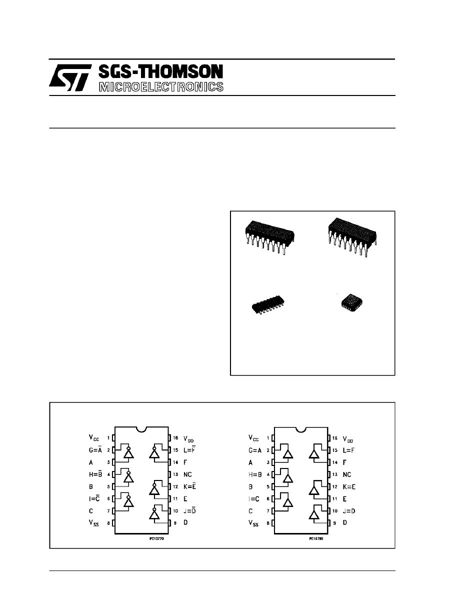
PIN CONNECTIONS
The HCC4009UB/4010B (extended temperature
range) and the HCF4009UB/4010B (intermediate
temperature range) are monolithic integrated cir-
cuits available in 16-lead dual in line plastic or ce-
ramic packages and plastic micropackage.
The HCC/HCF4009UB/4010B are inverting and
.
CMOS TO DTL/TTL HEX CONVERTER
.
HIGH-TO-LOW LEVEL LOGIC CONVERSION
.
MULTIPLEXER: 1-TO-6 OR 6-TO-1
.
HIGH”SINK” AND ”SOURCE” CURRENT CA-
PABILITY
.
5V, 10V AND 15V PARAMETRIC RATINGS
.
MAXIMUM INPUT CURRENT OF 100
µ
A AT
18V OVER FULL
.
PACKAGE AND TEMPERATURE RANGE;
100nA AT 18V AND 25
o
C
.
100% TESTED FOR QUIESCENT CURRENT
AT 20V
.
MEETS ALL REQUIREMENTS OF JEDEC TEN-
TATIVE STANDARD N. 13A, ” STANDARD
SPECIFICATIONS FOR DESCRIPTION OF B
SERIES CMOS DEVICES ”
4009UB–INVERTING TYPE
4010B–NON INVERTING TYPE
non-inverting Hex Buffer/Converters, respectively.
Both devices can be used as CMOS to TTL or DTL
logic-level converters, as current ”sink” or ”source”
drivers or as multiplexer (1 to 6).
4049UB and 4050B are prefered replacements for
4009UB and 4010B, respectively, in buffer applica-
tions.
4009UB
4010B
1/13
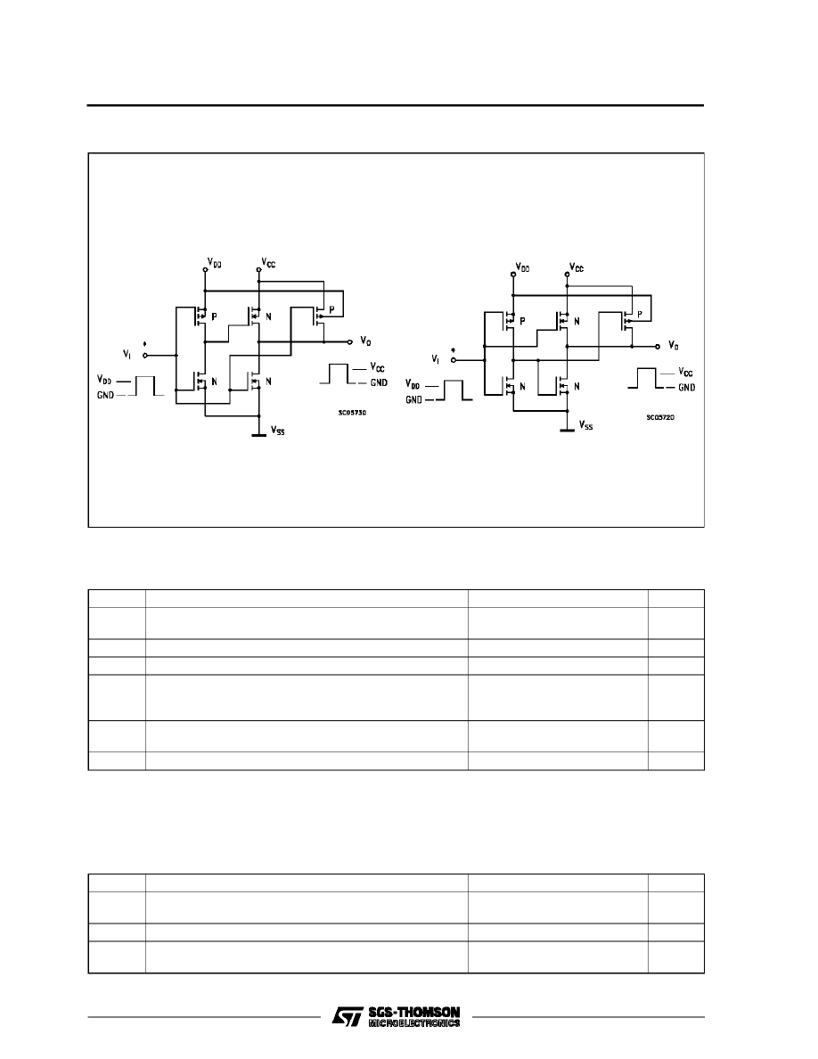
SCHEMATIC DIAGRAM: COS/MOS TO DTL OR TTL CONVERTER (1 of 6 identical units)
ABSOLUTE MAXIMUM RATING
Symbol
Parameter
Value
Unit
V
DD
*
Supply Voltage: HCC Types
HCF Types
-0.5 to +20
-0.5 to +18
V
V
V
i
Input Voltage
-0.5 to V
DD
+ 0.5
V
I
I
DC Input Current (any one input)
±
10
mA
P
tot
Total Power Dissipation (per package)
Dissipation per Output Transistor
for Top = Full Package Temperature Range
200
100
mW
mW
T
op
Operating Temperature: HCC Types
HCF Types
-55 to +125
-40 to +85
o
C
o
C
T
stg
Storage Temperature
-65 to +150
o
C
Stresses above those listed under ”Absolute Maximum Ratings” may cause permanent damage to the device. This is a stress ratingonly and functional
operation of the device at these or any other conditions above those indicated in the operational sections of this specification is not implied. Exposure
to absolute maximum rating conditions for external periods may affect device reliability.
* All voltage values are referred to V
SS
pin voltage.
RECOMMENDED OPERATING CONDITIONS
Symbol
Parameter
Value
Unit
V
DD
Supply Voltage: HCC Types
HCF Types
3 to 18
3 to 15
V
V
V
I
Input Voltage
0 to V
DD
V
T
op
Operating Temperature: HCC Types
HCF Types
-55 to +125
-40 to +85
o
C
o
C
Connect V
CC
to DTL or TTL supply and V
DD
to COS/MOS supply
4009UB
4010B
HCC/HCF4009UB HCC/ HCF4010B
2/13
STATIC ELECTRICAL CHARACTERISTICS (over recommended operating conditions)
Symbol
Parameter
Test Conditios
Value
Unit
V
I
(V)
V
O
(V)
|I
O
|
(
µ
A)
V
DD
(V)
T
LOW
*
25
o
C
T
HIGH
*
Min.
Max.
Min.
Typ.
Max.
Min.
Max.
I
L
Quiescent
Current
HCC
Types
0/5
5
1
0.02
1
30
µ
A
0/10
10
2
0.02
2
60
0/15
15
4
0.02
4
120
0/20
20
20
0.04
20
600
HCF
Types
0/5
5
4
0.02
4
30
0/10
10
8
0.02
8
60
0/15
15
16
0.02
16
120
V
OH
Output High
Voltage
0/5
5
4.95
4.95
4.95
V
0/10
10
9.95
9.95
9.95
0/15
15
14.95
14.95
14.95
V
OL
Output Low
Voltage
5/0
5
0.05
0.05
0.05
V
10/0
10
0.05
0.05
0.05
15/0
15
0.05
0.05
0.05
V
IH
Input High
Voltage (4009UB)
0.5
5
4
4
4
V
1
10
8
8
8
1.5
15
12.5
12.5
12.5
V
IH
Input High
Voltage (4010B)
4.5
5
3.5
3.5
3.5
V
9
10
7
7
7
13.5
15
11
11
11
V
IL
Input Low
Voltage (4009UB)
4.5
5
1
1
1
V
9
10
2
2
2
13.5
15
2.5
2.5
2.5
V
IL
Input Low
Voltage (4010B)
0.5
5
1.5
1.5
1.5
V
1
10
3
3
3
1.5
15
4
4
4
I
OH
Output
Drive
Current
HCC
Types
0/5
2.5
5
-1
-0.8
-1.6
-0.58
mA
0/5
4.6
5
-0.25
-0.2
-0.4
-0.15
0/10
9.5
10
-0.55
-0.45
-0.9
-0.33
0/15
13.5
15
-1.65
-1.5
-3
-1.1
HCF
Types
0/5
2.5
5
-0.9
-0.8
-1.6
-0.65
0/5
4.6
5
-0.23
-0.2
-0.4
-0.18
0/10
9.5
10
-0.5
-0.45
-0.9
-0.38
0/15
13.5
15
-1.6
-1.5
-3
-1.25
I
OL
Output
Sink
Current
HCC
Types
0/5
0.4
5
3.75
3
4
2.1
mA
0/10
0.5
10
10
8
10
5.6
0/15
1.5
15
30
24
36
16
HCF
Types
0/5
0.4
5
3.6
3
4
2.4
0/10
0.5
10
0.96
8
10
6.4
0/15
1.5
15
40
24
36
1.9
I
IH
, I
IL
Input Leakage
Current
0/18
18
±
0.1
±
10
-5
±
0.1
±
1
µ
A
C
I
Input
Capacitance
4009UB
Any Input
15
22.6
4010B
5
7.5
pF
* T
LOW
= -55
o
C for HCC device: -40
o
C for HCF device.
* T
HIGH
= +125
o
C for HCC device: +85
o
C for HCF device.
The Noise Margin for both ”1” and ”0” level is: 1V min. with V
DD
= 5 V, 2 V min. with V
DD
= 10 V, 2.5 V min. with V
DD
= 15 V
HCC/HCF4009UB HCC/HCF4010B
3/13
DYNAMIC ELECTRICAL CHARACTERISTICS (T
amb
= 25
o
C, C
L
= 50 pF, R
L
= 200 K
Ω
,
typical temperature coefficent for all V
DD
values is 03 %/
o
C, all input rise and fall times= 20 ns)
Symbol
Parameter
Test Conditions
Value
Unit
V
DD
(V)
V
I
(V)
V
CC
(V)
Min.
Typ.
Max.
t
PLH
Propagation Delay Time
(4009UB)
5
5
5
70
140
ns
10
10
10
40
80
10
10
5
35
70
15
15
15
30
60
15
15
5
30
60
t
PLH
Propagation Delay Time
(4010B)
5
5
5
100
200
ns
10
10
10
50
100
10
10
5
50
100
15
15
15
35
70
15
15
5
35
70
t
PHL
Propagation Delay Time
(4009UB)
5
5
5
30
60
ns
10
10
10
20
40
10
10
5
15
30
15
15
15
15
30
15
15
5
10
20
t
PHL
Propagation Delay Time
(4010B)
5
5
5
65
130
ns
10
10
10
35
70
10
10
5
30
70
15
15
15
25
50
15
15
5
20
40
t
TLH
Transition Time
5
5
5
150
350
ns
10
10
10
75
150
15
15
15
55
110
t
THL
Transition Time
5
5
5
35
70
ns
10
10
10
20
40
15
15
15
15
30
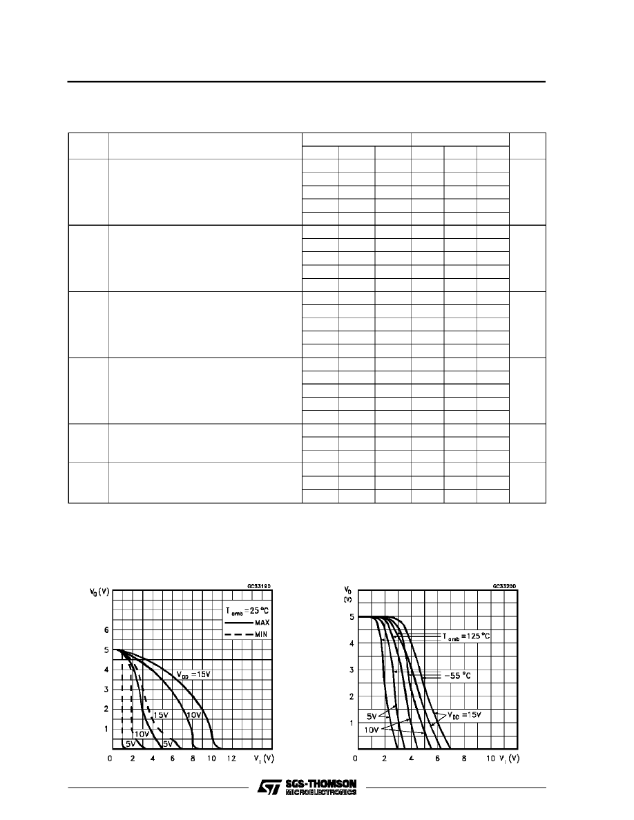
Minimum and Maximum Voltage Transfer Char-
acteristics for 4009UB
Typical Voltage Transfer Characteristics As a
Function of Temperature for 4009UB
HCC/HCF4009UB HCC/ HCF4010B
4/13
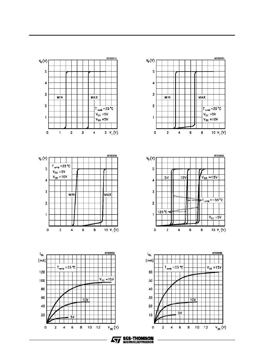
Minimum and Maximum Voltage Transfer Char-
acteristics for 4010B
Minimum and Maximum Voltage Transfer Char-
acteristics for 4010B
Typical Output Los (sink) Current Characteristics
Minimum and Maximum Voltage Transfer Char-
acteristics for 4010B
Typical Voltage Transfer Characteristics As a
Function ot Temperature for 4010B
Minimum output Low (sink) Current Charac-
teristics
HCC/HCF4009UB HCC/HCF4010B
5/13
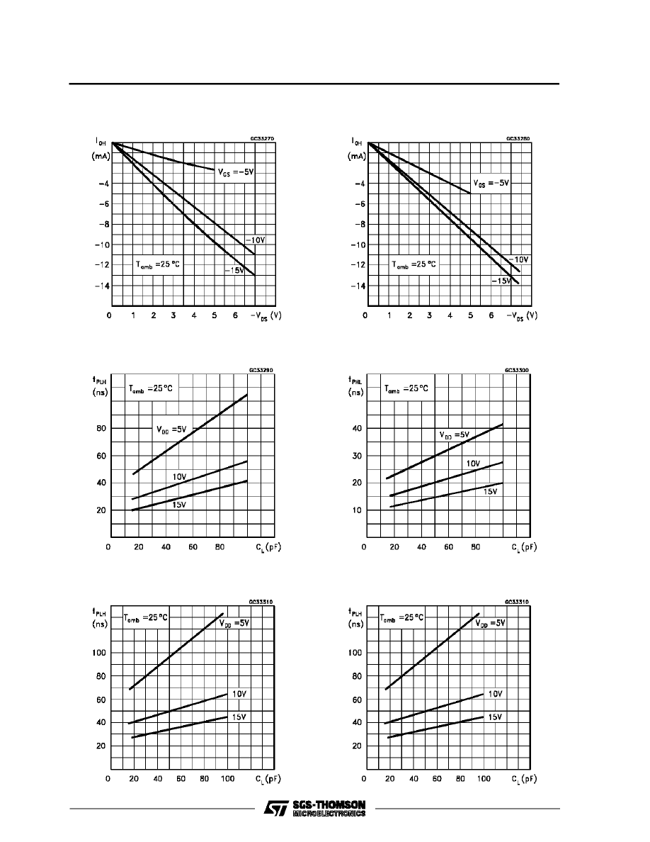
Typical Output High (source) Current Charac-
teristics
Typical Low to High Propagation Delay Time vs
Load Capacitance for 4009UB
Typical Low to High Propagation Delay Time vs
Load Capacitance for 4010B
Minimum output High (source) Current Charac-
teristics
Typical High to Low Propagation Delay Time vs
Load Capacitance for 4009UB
typical High to Low Propagation Delay Time vs
Load Capacitance for 4010B
HCC/HCF4009UB HCC/ HCF4010B
6/13
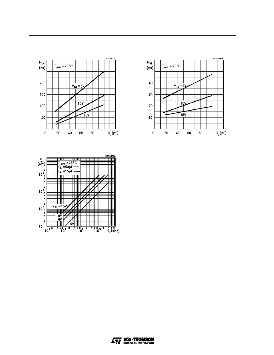
Typical Low to High Transition Time vs Load Ca-
pacitance
Typical High to Low Transition Time vs Load Ca-
pacitance
Typical Dissipation Characteristics
HCC/HCF4009UB HCC/HCF4010B
7/13
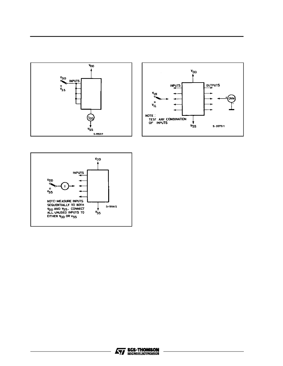
Quiescent Device Current.
Noise Immunity.
Input Leakage Current.
TEST CIRCUITS
HCC/HCF4009UB HCC/ HCF4010B
8/13
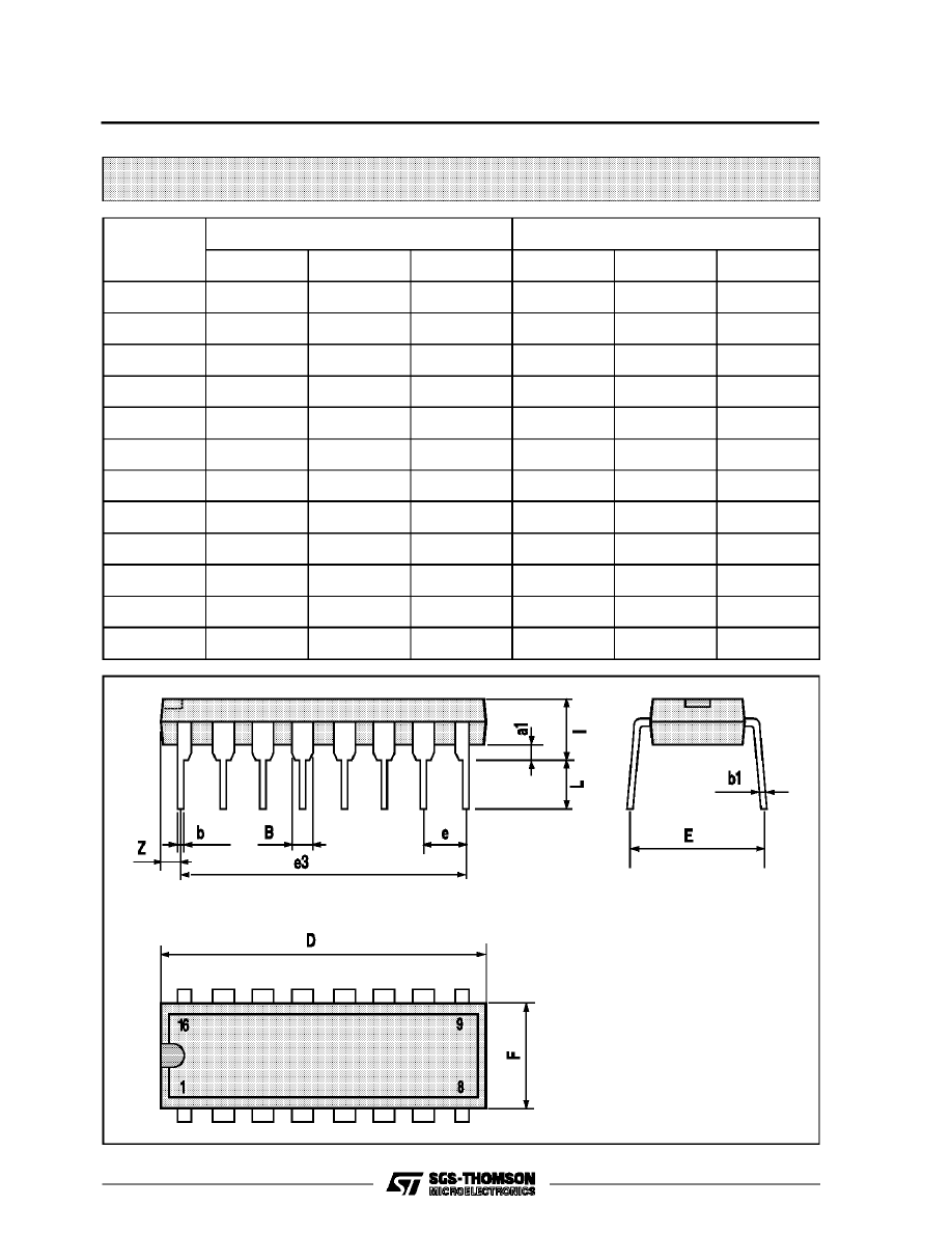
Plastic DIP16 (0.25) MECHANICAL DATA
DIM.
mm
inch
MIN.
TYP.
MAX.
MIN.
TYP.
MAX.
a1
0.51
0.020
B
0.77
1.65
0.030
0.065
b
0.5
0.020
b1
0.25
0.010
D
20
0.787
E
8.5
0.335
e
2.54
0.100
e3
17.78
0.700
F
7.1
0.280
I
5.1
0.201
L
3.3
0.130
Z
1.27
0.050
P001C
HCC/HCF4009UB HCC/HCF4010B
9/13
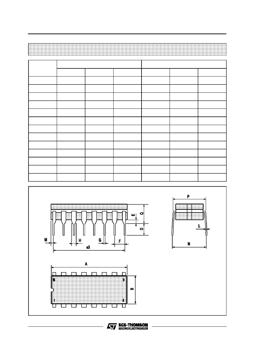
Ceramic DIP16/1 MECHANICAL DATA
DIM.
mm
inch
MIN.
TYP.
MAX.
MIN.
TYP.
MAX.
A
20
0.787
B
7
0.276
D
3.3
0.130
E
0.38
0.015
e3
17.78
0.700
F
2.29
2.79
0.090
0.110
G
0.4
0.55
0.016
0.022
H
1.17
1.52
0.046
0.060
L
0.22
0.31
0.009
0.012
M
0.51
1.27
0.020
0.050
N
10.3
0.406
P
7.8
8.05
0.307
0.317
Q
5.08
0.200
P053D
HCC/HCF4009UB HCC/ HCF4010B
10/13
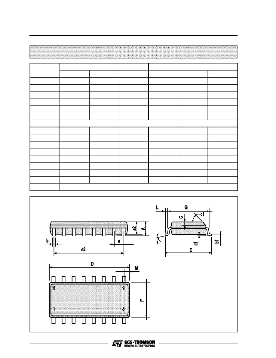
SO16 (Narrow) MECHANICAL DATA
DIM.
mm
inch
MIN.
TYP.
MAX.
MIN.
TYP.
MAX.
A
1.75
0.068
a1
0.1
0.2
0.004
0.007
a2
1.65
0.064
b
0.35
0.46
0.013
0.018
b1
0.19
0.25
0.007
0.010
C
0.5
0.019
c1
45
°
(typ.)
D
9.8
10
0.385
0.393
E
5.8
6.2
0.228
0.244
e
1.27
0.050
e3
8.89
0.350
F
3.8
4.0
0.149
0.157
G
4.6
5.3
0.181
0.208
L
0.5
1.27
0.019
0.050
M
0.62
0.024
S
8
°
(max.)
P013H
HCC/HCF4009UB HCC/HCF4010B
11/13
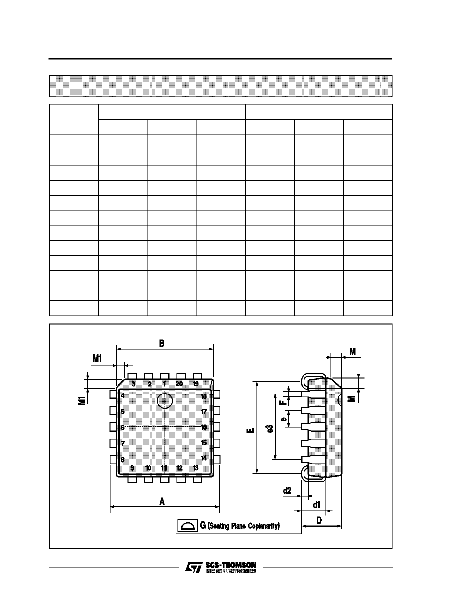
PLCC20 MECHANICAL DATA
DIM.
mm
inch
MIN.
TYP.
MAX.
MIN.
TYP.
MAX.
A
9.78
10.03
0.385
0.395
B
8.89
9.04
0.350
0.356
D
4.2
4.57
0.165
0.180
d1
2.54
0.100
d2
0.56
0.022
E
7.37
8.38
0.290
0.330
e
1.27
0.050
e3
5.08
0.200
F
0.38
0.015
G
0.101
0.004
M
1.27
0.050
M1
1.14
0.045
P027A
HCC/HCF4009UB HCC/ HCF4010B
12/13

Information furnished is believed to be accurate and reliable. However, SGS-THOMSON Microelectronics assumes no responsability for the
consequences of use of such information nor for any infringement of patents or other rights of third parties which may results from its use. No
license is granted by implication or otherwise under any patent or patent rights of SGS-THOMSON Microelectronics. Specifications mentioned
in this publication are subject to change without notice. This publication supersedes and replaces all information previously supplied.
SGS-THOMSON Microelectronics products are not authorized for use as critical components in life support devices or systems without express
written approval of SGS-THOMSON Microelectonics.
1994 SGS-THOMSON Microelectronics - All Rights Reserved
SGS-THOMSON Microelectronics GROUP OF COMPANIES
Australia - Brazil - France - Germany - Hong Kong - Italy - Japan - Korea - Malaysia - Malta - Morocco - The Netherlands -
Singapore - Spain - Sweden - Switzerland - Taiwan - Thailand - United Kingdom - U.S.A
HCC/HCF4009UB HCC/HCF4010B
13/13
Wyszukiwarka
Podobne podstrony:
025 odpowiedzialnosc cywilnaid 4009 ppt
4009
4009 a
4009
4009
4009
4009
4009
4009
4009
4009
025 odpowiedzialnosc cywilnaid 4009 ppt
Ulotka 5422 20180719000000 4009 N 20180802000537 Polfilin
więcej podobnych podstron