
AVR091: Replacing AT90S2313 by ATtiny2313
Features
•
AT90S2313 Errata Corrected in ATtiny2313
•
Changes to Bit and Register Names
•
Changes to Interrupt Vector
•
Oscillators and Selecting Start-up Delays
•
Improvements to Timer/Counters and Prescalers
•
Improvements to the U(S)ART
•
Enhanced Watchdog Timer
•
Changes to EEPROM Writing
•
Programming Interface
•
Operational Voltage Ranges
•
Changes to Electrical Characteristics
Introduction
This application note is a guide to help current AT90S2313 users convert existing
designs to ATtiny2313.
In addition to the differences described in this document, the electrical characteristics
of the devices are different. Check the datasheets for detailed information.
Improvements or added features in the AT90S2313 that are not in conflict with those
in AT90S1200 are not listed in this document.
Rev. 4298A–AVR–10/03
8-bit
Microcontrollers
Application Note

2
AVR091
4298A–AVR–10/03
AT90S2313 Errata
Corrected in
ATtiny2313
The following items from the Errata Sheets of the AT90S2313 do not apply to the
ATtiny2313. Refer to the AT90S2313 Errata Sheet for more details.
Releasing Reset
Condition without Clock
ATtiny2313 has a new reset circuit, which for any External Reset Pulse exceeding the
minimum pulse width t
RST
causes an internal reset even though the condition disap-
pears before any valid clock is present.
Lock Bits at High V
CC
In ATtiny2313, the Lock Bits can be cleared at any voltage level within the operating
range.
Reset During EEPROM
Write
In ATtiny2313, the erroneous behavior of the EEPROM address register is no longer an
issue. See the datasheet for general information about preventing EEPROM corruption.
Serial Programming at
Voltages below 2.9V
In relation to the serial programming there are no restrictions on the supply voltage or
system frequency as long as the device is operated within the voltage and frequency
range specified in the data sheet for the ATtiny2313.
UART Looses
Synchronization if RXD
Line is Low when UART
Receive is Disabled
The UART is replaced with a USART, which does not have this problem. The starting
edge of a reception is only accepted as valid if the Receive Enable bit in the USART
Control Register is set.
Changes to Names
The following control bits have changed names, but have the same functionality and
placement when accessed as in AT90S2313. These AT90S1200 bit definitions can
therefore be added to the ATtiny2313 definitions file, so no rewriting of the application
code is necessary.
Table 1. Changed Bit Names
Bit Name in AT90S2313
Bit Name in ATtiny2313
I/O Register (AT90S2313)
TICIE1
ICIE1
TIMSK
SM
SM0
MCUCR
PWM10 WGM10
TCCR1A
PWM11
WGM11
TCCR1A
CTC1
WGM12
TCCR1B
WDTOE
WDCE
WDTCR
EEWE
EEPE
EECR
EEMWE
EEMPE
EECR
OR
DOR
USR
CHR9
UCSZ2
UCR

3
AVR091
4298A–AVR–10/03
The following I/O Registers have changed names on ATtiny2313, but include the same
functionality and location when accessed as in AT90S2313.
Table 2. Changed Register Names
Changes to Interrupt
Vector
The interrupt vector table of the ATtiny2313 differs from the one of AT90S2313. These
changes mainly consist of addition of new interrupt vectors.
Table 3. Changes to Interrupt Vectors
Register Name AT90S2313
Register Name ATtiny2313
USR
UCSRA
UCR
UCSRB
UBRR
UBRRL
Vector No.
Program Address
AT90S2313
ATtiny2313
1
0x0000
RESET
RESET
2
0x0001
INT0
INT0
3
0x0002
INT1
INT1
4
0x0003
TIMER1 CAPT1
TIMER1 CAPT
5
0x0004
TIMER1 COMP1
TIMER1 COMPA
6
0x0005
TIMER1 OVF1
TIMER1 OVF
7
0x0006
TIMER0 OVF0
TIMER0 OVF
8
0x0007
UART RX
USART0 RX
9
0x0008
UART UDRE
USART0 UDRE
10
0x0009
UART TX
USART0 TX
11
0x000A
ANA_COMP
ANALOG COMP
12
0x000B
PCINT
13
0x000C
TIMER1 COMPB
14
0x000D
TIMER0 COMPA
15
0x000E
TIMER0 COMPB
16
0x000F
USI START
17
0x0010
USI OVERFLOW
18
0x0011
EE READY
19
0x0012
WDT OVERFLOW

4
AVR091
4298A–AVR–10/03
Oscillators and
Selecting Start-up
Delays
ATtiny2313 provides more Oscillators and Start-up Time options than AT90S2313.
The default clock source setting on ATtiny2313 is 1 MHz sourced from the Internal RC
Oscillator. The internal RC oscillator is set to run at 8 MHz, but with the system clock
prescaling preset to divide by 8. The default start-up delay is 65ms. There is no setting
that results in a 16ms startup delay; 4ms or 64ms must be selected.
Fuses must be programmed to enable the ATtiny2313 to use the XTAL1 and XTAL2
pins as clock source as on the AT90S2313. The correct fuse setting for ATtiny2313
depend on if the selected clock source is external clock or a crystal oscillator, and which
frequency it will be running at.
During wake-up from Power-down mode, the ATtiny2313 uses the CPU frequency to
determine the delay of the wake-up delay, while AT90S2313 determines the delay from
the WDT Oscillator frequency.
Follow the guidelines from the section “System Clock and Clock Options” in the
ATtiny2313 data sheet to find appropriate clock settings and start-up values.
The crystal Oscillator in AT90S2313 is capable of driving an additional clock buffer from
the XTAL2 output. The ATtiny2313 does not have a rail-to-rail swing on oscillator pins
and can therefore not be used for this purpose. Note however that the new Clock Out
(CKOUT) feature could alternatively be used to drive an additional clock buffer. CKOUT
is located on PD2, which also is used for the External Interrupt 0.
Improvements to
Timer/Counters and
Prescalers
For details about the improved and additional features, please refer to the data sheet.
The following features have been added:
•
The Prescalers in ATtiny2313 can be reset.
•
Variable top value in PWM mode.
•
For Timer/Counter1, Phase and Frequency Correct PWM mode in addition to the
Phase Correct PWM mode.
•
Fast PWM mode.
•
Timer0 extended with PWM and Output Compare function.
Differences Between
ATtiny2313 and
AT90S2313
Most of the improvements and changes apply to all the Timer/Counters and the descrip-
tion below is written in a general form. A lower case “x” replaces the output channel (x =
A or B), while “n” replaces the Timer/Counter number (n = 0 or 1).
TCNT1 Cleared in PWM Mode
In AT90S2313 there are three different PWM resolutions – 8, 9, or 10 bits. Even if only
8, 9, or 10 bits are compared, it is still possible to write values into the TCNT1 Register
that exceed the resolution. Thus, the Timer/Counter has to complete the count to
0xFFFF before the reduced resolution becomes effective (i.e. if 8-bit resolution is
selected and the TCNT1 Register contains 0x0100, the top value (0x00FF) will not be
effective until the counter has counted up to 0xFFFF, turned, and counted down to
0x0000 again). In ATtiny2313 this has been changed so that the unused bits in TCNT1
are being cleared to zero to avoid this unintended counting up to 0xFFFF. In the
ATtiny2313, the TCNT1 Register never exceeds the selected resolution.
OCR1xH Cleared in PWM
Mode
Clearing OCR1xH in PWM mode is slightly different from clearing TCNT1. The
AT90S2313 clears the six most significant bits if 8, 9, or 10 bits PWM mode is selected.
Hence, if 0xFFFF is written to OCR1x in PWM-mode and OCR1x is read back, the result
is 0x03FF regardless of which PWM mode that is selected. In ATtiny2313 the number of
cleared bits depends on the resolution.
5
AVR091
4298A–AVR–10/03
Clear Timer/Counter on
Compare Match with
Prescaler
The relation between a Clear on Compare match and the internal counting of the
Timer/Counters has been changed. The Clear on Compare Match in the AT90S2313
clears the Timer/Counter after the first internal count matching the compare value,
whereas the ATtiny2313 clears Timer/Counter after the last internal count matching the
compare value. See Figure 1 and Figure 2 for details on clearing, flag setting, and pin
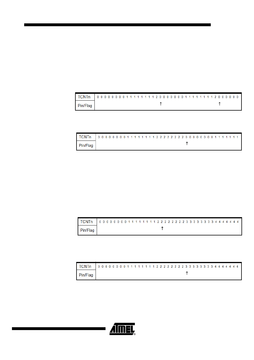
change. Example: OCR1x = 0x02 when prescaler is enabled (divide clock by 8).
Figure 1. Setting Output Compare Flag/Pin for AT90S2313. “
↑
Indicates where the Output Compare Flag/Pin will be set
Figure 2.
Setting Output Compare Flag/Pin for ATtiny2313. “
↑
Indicates where the Output Compare Flag/Pin will be set .
Setting of Output Compare
Pin/Flag with Prescaler
Enabled (Applies to all
Timer/Counters)
The relation between an Output Compare event and the internal counting of the
Timer/Counter has been changed. Output Compare in the AT90S2313 sets the Output
Compare pin/flag after the first internal count matching the compare value, whereas the
ATtiny2313 sets the Output Compare pin/flag after the last internal count matching the
compare value. See Figure 3 and Figure 4 for details on Output Compare Flag setting
and pin change. Example: OCR1x = 0x02, prescaler enabled (divide clock by 8).
Figure 3. Figure 3 Setting Output Compare Flag/Pin for AT90S2313. “
↑
Indicates where the Output Compare Flag/Pin will
be set.
Figure 4.
Setting Output Compare Flag/Pin for ATtiny2313. “
↑
Indicates where the Output Compare Flag/Pin will be set.
Write to OCR1x in PWM Mode,
Change to Normal Mode
Before OCR1x is Updated at
the Top, Read OCR1x
As described in the data sheet, the OCR1x Registers are updated at the top value when
written. Thus, when writing the OCR1x in PWM mode, the value is stored in a temporary
buffer. When the Timer/Counter reaches the top, the temporary buffer is transferred to
the actual Output Compare Register. If PWM mode is left after the temporary buffer is
written, but before the actual Output Compare Register is updated, the behavior differs
between ATtiny2313 and AT90S2313.

6
AVR091
4298A–AVR–10/03
ATtiny2313
If the OCR1x Register is read before the update is done, the actual compare value is
read – not the temporary OCR1x buffer.
AT90S2313
If the OCR1x Register is read before the update is done, the value in the OCR1x buffer
is read. For example, the value read is the one last written (to the OCR1x buffer), but
since the Timer/Counter never reached the top value, it was not latched into the OCR1x
Register. Hence, the value that is used for comparison is not necessarily the same as
being read.
Note: This applies to 16-bit Timer/Counter only, for 8-bit Timer/Counter, the temporary
buffer is read in both devices.
Memory of Previous OCnx pin
Level
In AT90S2313, there are two settings of COMnx1:0 that do not update the OCnx pin in
PWM mode (0b00 and 0b01), and one setting of COMnx1:0 in non-PWM mode (0b00).
Assume the Timer/Counter is taken from a state that updates the OCnx pin to a state
that does not, and then back again to a state that does update the OCnx pin. The follow-
ing differences should be noted:
ATtiny2313
The level of the OCnx-pin before disabling the Output Compare mode is remembered.
Re-enabling the Output Compare mode will cause the OCnx pin to resume operation
from the state it had when it was disabled. All Output Compare pins are initialized to
zero on Reset.
AT90S2313
For Timer/Counter1 in non-PWM mode, a compare match during the time when the
Timer/Counter is not connected to the pin will reset the OCnx pin to the low level once
enabled again. PWM mode will update the internal register for the OCnx pin, such that
the state of the pin is unknown once enabled again.
Improvements to the
U(S)ART
The UART in AT90S2313 has been replaced by a USART in ATtiny2313. The
ATtiny2313 USART is compatible with the AT90S2313 UART with one exception: The
two-level Receive Register acts as a FIFO.
The following must be kept in mind:
A second buffer register has been added. The two buffer registers operate as a circular
FIFO buffer. Therefore the UDR must only be read once for each incoming data. More
important is the fact that the Error Flags (FE and DOR) and the ninth data bit (RXB8) are
buffered with the data in the receive buffer. Therefore the status bits must always be
read before the UDR Register is read. Otherwise the error status will be lost since the
buffer state is lost.
The Receiver Shift Register can now act as a third buffer level. This is done by allowing
the received data to remain in the Serial Shift Register if the buffer registers are full, until
a new start bit is detected. The USART is therefore more resistant to Data OverRun
(DOR) error conditions.
Another minor difference is the initial value of RXB8, which is “1” in the UART in
AT90S2313 and “0” in the USART in ATtiny2313.
The USART has a new Double Speed mode, which allows a higher communication
speed.
Enhanced Watchdog
Timer
The ATtiny2313 has the Enhanced Watchdog Timer (WDT) and is improved compared
to the one in AT90S2313.

7
AVR091
4298A–AVR–10/03
If the WDT is not used, it is still recommended to disable it initially in the application code
to clear unintentional WDT enabled events.
If the operation voltage is 5V and the WDTON fuse is left unprogrammed, the WDT will
behave similar on AT90S2313 and ATtiny2313.
The frequency of the Watchdog Oscillator in ATtiny2313 is approximately 128kHz for all
supply voltages. The typical frequency of the Watchdog Oscillator in AT90S2313 is
close to 1.0 MHz at 5V, but the Time-out period increases with decreasing VCC. This
means that the selection of Time-out period for the Watchdog Timer (in terms of number
of WDT Oscillator cycles) must be reconsidered when porting the design to ATtiny2313.
In AT90S2313, the Watchdog Timer is either enabled or disabled, while ATtiny2313
supports two safety levels selected by the WDTON Fuse.
Refer to the ATtiny2313 datasheet or the Application note “AVR132 – Enhanced Watch-
dog Timer” for more information.
Changes to EEPROM
Writing
In AT90S2313, the EEPROM write time is dependent on supply voltage, typically 2.5 ms
@ VCC = 5V and 4 ms @ VCC = 2.7V. It is the internal RC oscillator that sources the
EEPROM write time counter. The internal RC oscillator on ATtiny2313 is close to the
calibrated value for all supply voltages. In ATtiny2313, the EEPROM write time will
therefore always be 3.4ms.
Note: Changing the value in the OSCCAL Register affects the frequency of the cali-
brated RC Oscillator and hence the EEPROM write time.
Programming
Interface
Changes have been made to the programming interfaces. The changes are valid for
both serial programming (ISP) and parallel programming.
•
Programming of both flash and EEPROM is now done in pages instead of per byte.
The EEPROM can however also be programmed pr byte over the serial interface.
•
Added support for new fuses.
See the ATtiny2313 data sheet for details.
Fuse Settings
AT90S2313 has 2 fuses. ATtiny2313 has 17 fuses. These fuses control many of the
important features on the ATtiny2313 and setting of them is crucial for correct operation
of the device. The fuses on ATtiny2313 are listed in Table 4, Fuse settings on
ATtiny2313. Bits changed from default are marked in bold., together with a suggested
setting for “AT90S2313 compatibility”. See the datasheet for ATtiny2313 for more infor-
mation about the fuses.

8
AVR091
4298A–AVR–10/03
.
Table 4. Fuse settings on ATtiny2313. Bits changed from default are marked in bold
Fuse Byte
Bit
Name
Description
Default Value
(1)
AT90S2313
compatible
setting (1) (2)
E
x
te
nde
d Fu
s
e
By
te
7
–
–
1
1
6
–
–
1
1
5
–
–
1
1
4
–
–
1
1
3
–
–
1
1
2
–
–
1
1
1
–
–
1
1
0
SPMEN
Self
Programming
Enable
1 1
High
F
u
se Byte
7
DWEN
debugWIRE
Enable
1 1
6
EESAVE
EEPROM
memory is
preserved
through the
Chip Erase
1 1
5
SPIEN
Enable Serial
Program and
Data
Downloading
0 0
4
WDTON
Watchdog
Timer always
on
1 1
3
BODLEVEL2
Brown-out
Detector
trigger level
1 1
2
BODLEVEL1
Brown-out
Detector
trigger level
1 1
1
BODLEVEL0
Brown-out
Detector
trigger level
1 1
0
RSTDISBL
External Reset
disable
1 1

9
AVR091
4298A–AVR–10/03
Notes:
1. 0 = programmed, 1 = unprogrammed
2. Sets the clock setting for Crystal Oscillator 3-8 MHz, with startup time from reset to
14CK+65ms. Note that the default setting on AT90S2313 gives a startup time of
~16ms. Refer to the ATtiny2313 datasheet for more information on clock and startup
delay settings.
Low Fu
s
e
By
te
7
CKDIV8
Divide clock
by 8
0
1
6
CKOUT
Output Clock
on CKOUT pin
1 1
5
SUT1
Select start-up
time
1
0
4
SUT0
Select start-up
time
0
1
3
CKSEL3
Select Clock
source
0
1
2
CKSEL2
Select Clock
source
0
1
1
CKSEL1
Select Clock
source
1
0
0
CKSEL0
Select Clock
source
0 0
Table 4. Fuse settings on ATtiny2313. Bits changed from default are marked in bold
Fuse Byte
Bit
Name
Description
Default Value
(1)
AT90S2313
compatible
setting (1) (2)

10
AVR091
4298A–AVR–10/03
Device Signatures
AT90S2313 has Signature Bytes: 0x1E 0x91 0x01.
ATtiny2313 has Signature Bytes: 0x1E 0x91 0x0A.
Operational Voltage
Ranges
AT90S2313 can operate from 2.7 - 6.0V.
ATtiny2313 can operate from 1.8 - 5.5V.
Changes to Electrical
Characteristics
The ATtiny2313 is produced in a different process then the AT90S2313 and electrical
characteristics will differ between these devices. Please consult the data sheets for
details on electrical characteristics.

Printed on recycled paper.
Disclaimer: Atmel Corporation makes no warranty for the use of its products, other than those expressly contained in the Company’s standard
warranty which is detailed in Atmel’s Terms and Conditions located on the Company’s web site. The Company assumes no responsibility for any
errors which may appear in this document, reserves the right to change devices or specifications detailed herein at any time without notice, and
does not make any commitment to update the information contained herein. No licenses to patents or other intellectual property of Atmel are
granted by the Company in connection with the sale of Atmel products, expressly or by implication. Atmel’s products are not authorized for use
as critical components in life support devices or systems.
Atmel Corporation
Atmel Operations
2325 Orchard Parkway
San Jose, CA 95131, USA
Tel: 1(408) 441-0311
Fax: 1(408) 487-2600
Regional Headquarters
Europe
Atmel Sarl
Route des Arsenaux 41
Case Postale 80
CH-1705 Fribourg
Switzerland
Tel: (41) 26-426-5555
Fax: (41) 26-426-5500
Asia
Room 1219
Chinachem Golden Plaza
77 Mody Road Tsimshatsui
East Kowloon
Hong Kong
Tel: (852) 2721-9778
Fax: (852) 2722-1369
Japan
9F, Tonetsu Shinkawa Bldg.
1-24-8 Shinkawa
Chuo-ku, Tokyo 104-0033
Japan
Tel: (81) 3-3523-3551
Fax: (81) 3-3523-7581
Memory
2325 Orchard Parkway
San Jose, CA 95131, USA
Tel: 1(408) 441-0311
Fax: 1(408) 436-4314
Microcontrollers
2325 Orchard Parkway
San Jose, CA 95131, USA
Tel: 1(408) 441-0311
Fax: 1(408) 436-4314
La Chantrerie
BP 70602
44306 Nantes Cedex 3, France
Tel: (33) 2-40-18-18-18
Fax: (33) 2-40-18-19-60
ASIC/ASSP/Smart Cards
Zone Industrielle
13106 Rousset Cedex, France
Tel: (33) 4-42-53-60-00
Fax: (33) 4-42-53-60-01
1150 East Cheyenne Mtn. Blvd.
Colorado Springs, CO 80906, USA
Tel: 1(719) 576-3300
Fax: 1(719) 540-1759
Scottish Enterprise Technology Park
Maxwell Building
East Kilbride G75 0QR, Scotland
Tel: (44) 1355-803-000
Fax: (44) 1355-242-743
RF/Automotive
Theresienstrasse 2
Postfach 3535
74025 Heilbronn, Germany
Tel: (49) 71-31-67-0
Fax: (49) 71-31-67-2340
1150 East Cheyenne Mtn. Blvd.
Colorado Springs, CO 80906, USA
Tel: 1(719) 576-3300
Fax: 1(719) 540-1759
Biometrics/Imaging/Hi-Rel MPU/
High Speed Converters/RF Datacom
Avenue de Rochepleine
BP 123
38521 Saint-Egreve Cedex, France
Tel: (33) 4-76-58-30-00
Fax: (33) 4-76-58-34-80
Literature Requests
www.atmel.com/literature
4298A–AVR–10/03
© Atmel Corporation 2003. All rights reserved. Atmel
®
and combinations thereof AVR
®
and megaAVR
®
are the registered trademarks of Atmel
Corporation or its subsidiaries. Other terms and product names may be the trademarks of others.
Document Outline
- Features
- Introduction
- AT90S2313 Errata Corrected in ATtiny2313
- Changes to Names
- Changes to Interrupt Vector
- Oscillators and Selecting Start-up Delays
- Improvements to Timer/Counters and Prescalers
- Differences Between ATtiny2313 and AT90S2313
- TCNT1 Cleared in PWM Mode
- OCR1xH Cleared in PWM Mode
- Clear Timer/Counter on Compare Match with Prescaler
- Setting of Output Compare Pin/Flag with Prescaler Enabled (Applies to all Timer/Counters)
- Write to OCR1x in PWM Mode, Change to Normal Mode Before OCR1x is Updated at the Top, Read OCR1x
- Memory of Previous OCnx pin Level
- Differences Between ATtiny2313 and AT90S2313
- Improvements to the U(S)ART
- Enhanced Watchdog Timer
- Changes to EEPROM Writing
- Programming Interface
- Operational Voltage Ranges
- Changes to Electrical Characteristics
Wyszukiwarka
Podobne podstrony:
alternator replacement with wiring diagrhams
7 BEAUTY PRODUCTS TO REPLACE WITH TEA(1)
Advanced Polyphthalamide (PPA) Metal Replacement Trends
Image Processing with Matlab 33
L 5590 Short Sleeved Dress With Zipper Closure
M 5190 Long dress with a contrast finishing work
ARTICLE SUSPENSION STRUT FRONT REPLACE INSTALL
O'Reilly How To Build A FreeBSD STABLE Firewall With IPFILTER From The O'Reilly Anthology
M 5450 Dress with straps
Dance, Shield Modelling of sound ®elds in enclosed spaces with absorbent room surfaces
kurs excel (ebook) statistical analysis with excel X645FGGBVGDMICSVWEIYZHTBW6XRORTATG3KHTA
03 Teach Yourself Speak Greek With Confidence
Get Started with Dropbox
Osteochondritis dissecans in association with legg calve perthes disease
M 5588 Long Sleeveless Dress With Shaped Trim
Dealing with competency?sed questions
5 2 1 8 Lab Observing ARP with the Windows CLI, IOS CLI, and Wireshark
11 2 4 5 Lab ?cessing Network?vices with SSH
więcej podobnych podstron