2535CS–AVR–02/04
Features
•
High Performance, Low Power AVR
®
8-Bit Microcontroller
•
Advanced RISC Architecture
– 120 Powerful Instructions – Most Single Clock Cycle Execution
– 32 x 8 General Purpose Working Registers
– Fully Static Operation
•
Non-volatile Program and Data Memories
– 1K Byte of In-System Programmable Program Memory Flash
Endurance: 10,000 Write/Erase Cycles
– 64 Bytes In-System Programmable EEPROM
Endurance: 100,000 Write/Erase Cycles
– 64 Bytes Internal SRAM
– Programming Lock for Self-Programming Flash Program and EEPROM Data
Security
•
Peripheral Features
– One 8-bit Timer/Counter with Prescaler and Two PWM Channels
– 4-channel, 10-bit ADC with Internal Voltage Reference
– Programmable Watchdog Timer with Separate On-chip Oscillator
– On-chip Analog Comparator
•
Special Microcontroller Features
– debugWIRE On-chip Debug System
– In-System Programmable via SPI Port
– External and Internal Interrupt Sources
– Low Power Idle, ADC Noise Reduction, and Power-down Modes
– Enhanced Power-on Reset Circuit
– Programmable Brown-out Detection Circuit
– Internal Calibrated Oscillator
•
I/O and Packages
– 8-pin PDIP/SOIC: Six Programmable I/O Lines
•
Operating Voltage:
– 1.8 - 5.5V for ATtiny13V
– 2.7 - 5.5V for ATtiny13
•
Speed Grade
– ATtiny13V: 0 - 6 MHz @ 1.8 - 5.5V, 0 - 12 MHz @ 2.7 - 5.5V
– ATtiny13: 0 - 12 MHz @ 2.7 - 5.5V, 0 - 24 MHz @ 4.5 - 5.5V
•
Industrial Temperature Range
•
Low Power Consumption
– Active Mode:
1 MHz, 1.8V: 240µA
– Power-down Mode:
< 0.1µA at 1.8V
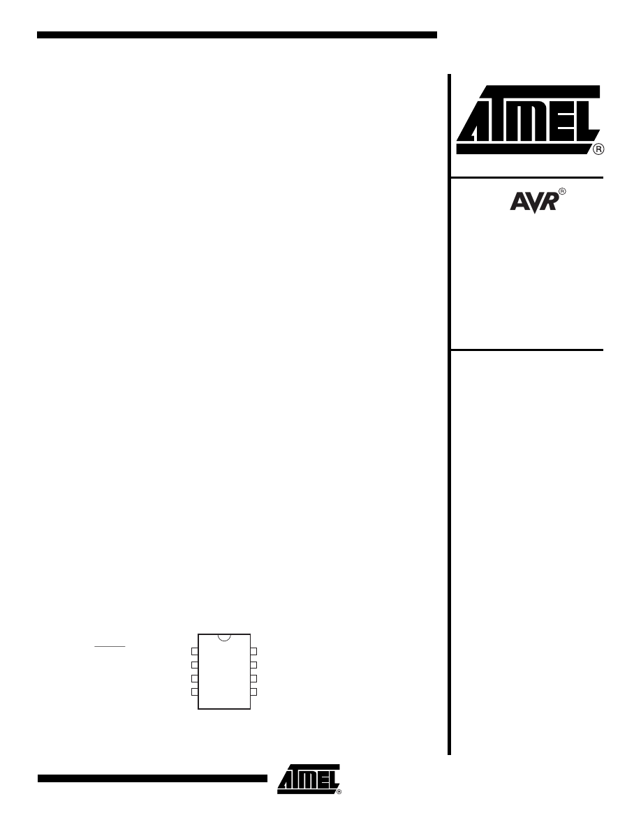
Pin Configurations
Figure 1. Pinout ATtiny13
1
2
3
4
8
7
6
5
(PCINT5/RESET/ADC0/dW) PB5
(PCINT3/CLKI/ADC3) PB3
(PCINT4/ADC2) PB4
GND
VCC
PB2 (SCK/ADC1/T0/PCINT2)
PB1 (MISO/AIN1/OC0B/INT0/PCINT1)
PB0 (MOSI/AIN0/OC0A/PCINT0)
PDIP/SOIC
8-bit
Microcontroller
with 1K Bytes
In-System
Programmable
Flash
ATtiny13
Preliminary
Summary
Rev. 2535CS–AVR–02/04
Note: This is a summary document. A complete document
is available on our Web site at www.atmel.com.
2
ATtiny13
2535CS–AVR–02/04
Overview
The ATtiny13 is a low-power CMOS 8-bit microcontroller based on the AVR enhanced
RISC architecture. By executing powerful instructions in a single clock cycle, the
ATtiny13 achieves throughputs approaching 1 MIPS per MHz allowing the system
designer to optimize power consumption versus processing speed.
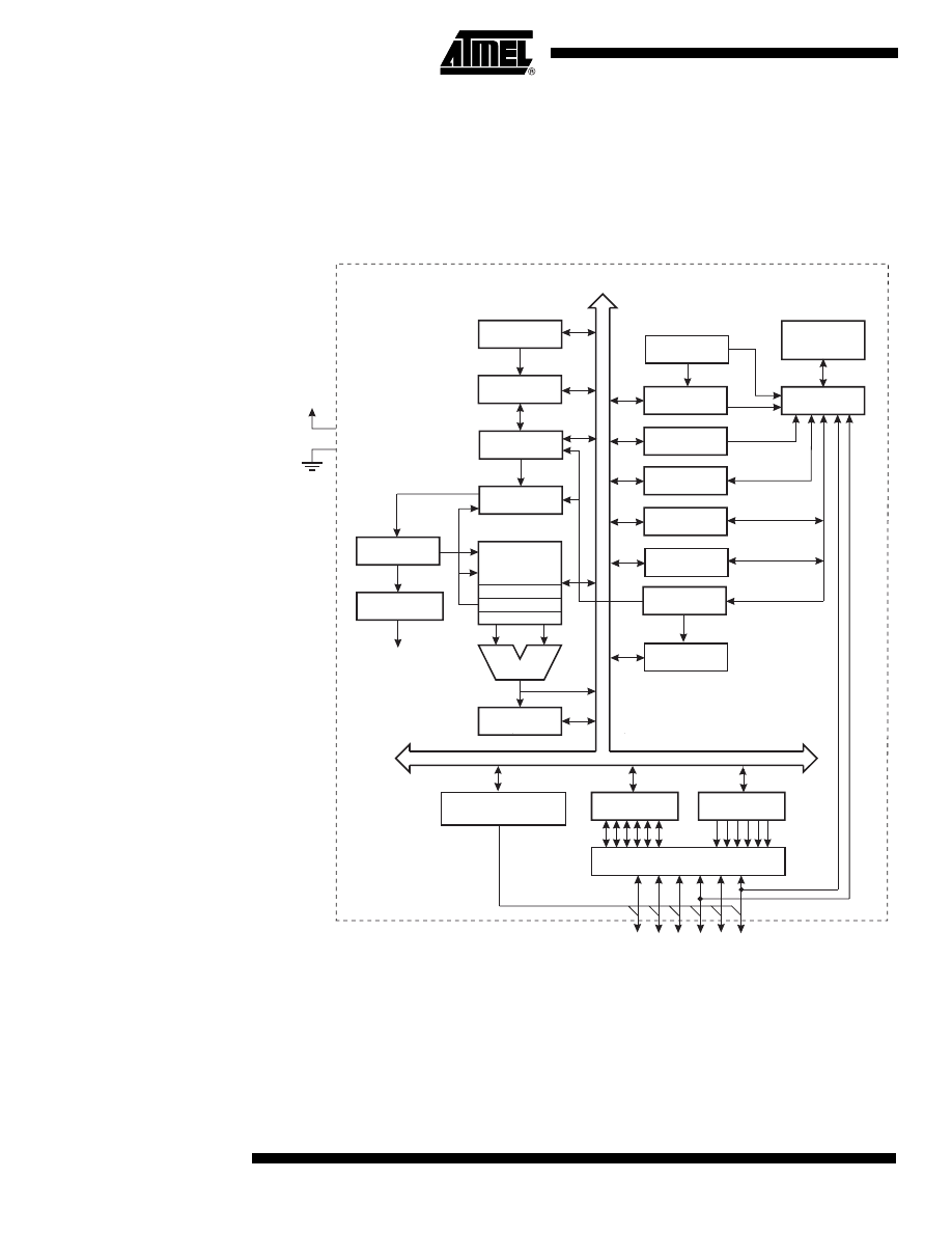
Block Diagram
Figure 2. Block Diagram
PROGRAM
COUNTER
INTERNAL
OSCILLATOR
WATCHDOG
TIMER
STACK
POINTER
PROGRAM
FLASH
SRAM
MCU CONTROL
REGISTER
GENERAL
PURPOSE
REGISTERS
INSTRUCTION
REGISTER
TIMER/
COUNTER0
INSTRUCTION
DECODER
DATA DIR.
REG.PORT B
DATA REGISTER
PORT B
PROGRAMMING
LOGIC
TIMING AND
CONTROL
MCU STATUS
REGISTER
STATUS
REGISTER
ALU
PORT B DRIVERS
PB0-PB5
VCC
GND
CONTROL
LINES
8-BIT DATABUS
Z
ADC /
ANALOG COMPARATOR
INTERRUPT
UNIT
CALIBRATED
Y
X
RESET
CLKI
WATCHDOG
OSCILLATOR
DATA
EEPROM

3
ATtiny13
2535CS–AVR–02/04
The AVR core combines a rich instruction set with 32 general purpose working registers.
All the 32 registers are directly connected to the Arithmetic Logic Unit (ALU), allowing
two independent registers to be accessed in one single instruction executed in one clock
cycle. The resulting architecture is more code efficient while achieving throughputs up to
ten times faster than conventional CISC microcontrollers.
The ATtiny13 provides the following features: 1K byte of In-System Programmable
Flash, 64 bytes EEPROM, 64 bytes SRAM, 6 general purpose I/O lines, 32 general pur-
pose working registers, one 8-bit Timer/Counter with compare modes, Internal and
External Interrupts, a 4-channel, 10-bit ADC, a programmable Watchdog Timer with
internal Oscillator, and three software selectable power saving modes. The Idle mode
stops the CPU while allowing the SRAM, Timer/Counter, ADC, Analog Comparator, and
Interrupt system to continue functioning. The Power-down mode saves the register con-
tents, disabling all chip functions until the next Interrupt or Hardware Reset. The ADC
Noise Reduction mode stops the CPU and all I/O modules except ADC, to minimize
switching noise during ADC conversions.
The device is manufactured using Atmel’s high density non-volatile memory technology.
The On-chip ISP Flash allows the Program memory to be re-programmed In-System
through an SPI serial interface, by a conventional non-volatile memory programmer or
by an On-chip boot code running on the AVR core.
The ATtiny13 AVR is supported with a full suite of program and system development
tools including: C Compilers, Macro Assemblers, Program Debugger/Simulators, In-Cir-
cuit Emulators, and Evaluation kits.
Pin Descriptions
VCC
Digital supply voltage.
GND
Ground.
Port B (PB5..PB0)
Port B is a 6-bit bi-directional I/O port with internal pull-up resistors (selected for each
bit). The Port B output buffers have symmetrical drive characteristics with both high sink
and source capability. As inputs, Port B pins that are externally pulled low will source
current if the pull-up resistors are activated. The Port B pins are tri-stated when a reset
condition becomes active, even if the clock is not running.
Port B also serves the functions of various special features of the ATtiny13 as listed on
page 49.
RESET
Reset input. A low level on this pin for longer than the minimum pulse length will gener-
ate a reset, even if the clock is not running. The minimum pulse length is given in Table
12 on page 30. Shorter pulses are not guaranteed to generate a reset.
4
ATtiny13
2535CS–AVR–02/04
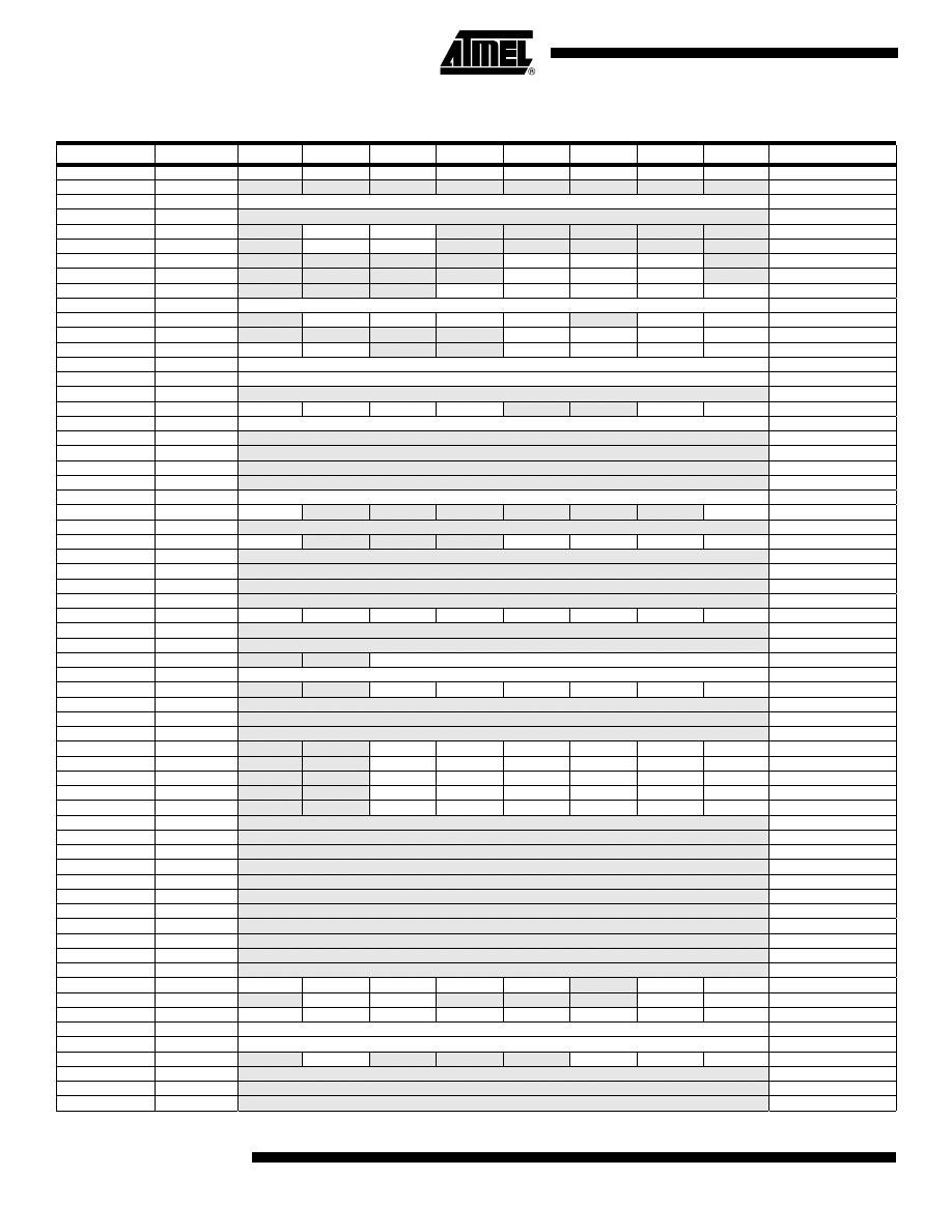
Register Summary
Address
Name
Bit 7
Bit 6
Bit 5
Bit 4
Bit 3
Bit 2
Bit 1
Bit 0
Page
0x3F
SREG
I
T
H
S
V
N
Z
C
page 6
0x3E
Reserved
–
–
–
–
–
–
–
–
0x3D
SPL
SP[7:0]
page 8
0x3C
Reserved
–
0x3B
GIMSK
–
INT0
PCIE
–
–
–
–
–
page 53
0x3A GIFR
–
INTF0
PCIF
–
–
–
–
–
page 53
0x39 TIMSK0
–
–
–
–
OCIE0B
OCIE0A
TOIE0
–
page 70
0x38 TIFR0
–
–
–
–
OCF0B
OCF0A
TOV0
–
page 71
0x37 SPMCSR
–
–
–
CTPB
RFLB
PGWRT
PGERS
SELFPRGEN
page 97
0x36
OCR0A
Timer/Counter – Output Compare Register A
page 70
0x35
MCUCR
–
PUD
SE
SM1
SM0
–
ISC01
ISC00
page 49
0x34 MCUSR
–
–
–
–
WDRF
BORF
EXTRF
PORF
page 33
0x33 TCCR0B
FOC0A
FOC0B
–
–
WGM02
CS02
CS01
CS00
page 66
0x32
TCNT0
Timer/Counter (8-bit)
page 70
0x31
OSCCAL
Oscillator Calibration Register
page 22
0x30 Reserved
–
0x2F
TCCR0A
COM0A1
COM0A0
COM0B1
COM0B0
–
–
WGM01
WGM00
page 69
0x2E
DWDR
DWDR[7:0]
page 94
0x2D
Reserved
–
0x2C
Reserved
–
0x2B
Reserved
–
0x2A Reserved
–
0x29
OCR0B
Timer/Counter – Output Compare Register B
page 70
0x28 GTCCR
TSM
–
–
–
–
–
–
PSR10
page 73
0x27 Reserved
–
0x26 CLKPR
CLKPCE
–
–
–
CLKPS3
CLKPS2
CLKPS1
CLKPS0
page 24
0x25
Reserved
–
0x24 Reserved
–
0x23 Reserved
–
0x22
Reserved
–
0x21 WDTCR
WDTIF
WDTIE
WDP3
WDCE
WDE
WDP2
WDP1
WDP0
page
37
0x20 Reserved
–
0x1F Reserved
–
0x1E
EEARL
–
–
EEPROM Address Register
page 14
0x1D
EEDR
EEPROM Data Register
page 14
0x1C
EECR
–
–
EEPM1
EEPM0
EERIE
EEMWE
EEWE
EERE
page 15
0x1B Reserved
–
0x1A
Reserved
–
0x19 Reserved
–
0x18 PORTB
–
–
PORTB5
PORTB4
PORTB3
PORTB2
PORTB1
PORTB0
page 51
0x17
DDRB
–
–
DDB5
DDB4
DDB3
DDB2
DDB1
DDB0
page 51
0x16 PINB
–
–
PINB5
PINB4
PINB3
PINB2
PINB1
PINB0
page 51
0x15
PCMSK
–
–
PCINT5
PCINT4
PCINT3
PCINT2
PCINT1
PCINT0
page 54
0x14 DIDR0
–
–
ADC0D
ADC2D
ADC3D
ADC1D
EIN1D
AIN0D
page 76, page 91
0x13 Reserved
–
0x12
Reserved
–
0x11 Reserved
–
0x10
Reserved
–
0x0F Reserved
–
0x0E Reserved
–
0x0D
Reserved
–
0x0C
Reserved
–
0x0B
Reserved
–
0x0A
Reserved
–
0x09
Reserved
–
0x08
ACSR
ACD
ACBG
ACO
ACI
ACIE
–
ACIS1
ACIS0
page 74
0x07
ADMUX
–
REFS0
ADLAR
–
–
–
MUX1
MUX0
page 88
0x06
ADCSRA
ADEN
ADSC
ADATE
ADIF
ADIE
ADPS2
ADPS1
ADPS0
page 89
0x05
ADCH
ADC Data Register High Byte
page 90
0x04
ADCL
ADC Data Register Low Byte
page 90
0x03
ADCSRB
–
ACME
–
–
–
ADTS2
ADTS1
ADTS0
page 91
0x02
Reserved
–
0x01
Reserved
–
0x00
Reserved
–

5
ATtiny13
2535CS–AVR–02/04
Note:
1. For compatibility with future devices, reserved bits should be written to zero if accessed. Reserved I/O memory addresses
should never be written.
2. I/O Registers within the address range 0x00 - 0x1F are directly bit-accessible using the SBI and CBI instructions. In these
registers, the value of single bits can be checked by using the SBIS and SBIC instructions.
3. Some of the Status Flags are cleared by writing a logical one to them. Note that, unlike most other AVRs, the CBI and SBI
instructions will only operation the specified bit, and can therefore be used on registers containing such Status Flags. The
CBI and SBI instructions work with registers 0x00 to 0x1F only.

6
ATtiny13
2535CS–AVR–02/04
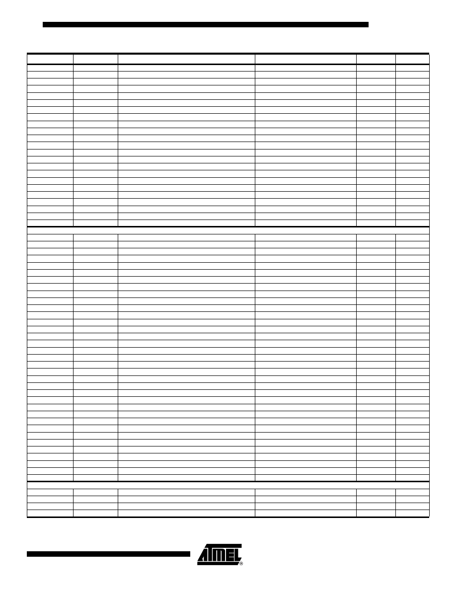
Instruction Set Summary
Mnemonics
Operands
Description
Operation
Flags
#Clocks
ARITHMETIC AND LOGIC INSTRUCTIONS
ADD
Rd, Rr
Add two Registers
Rd
← Rd + Rr
Z,C,N,V,H
1
ADC
Rd, Rr
Add with Carry two Registers
Rd
← Rd + Rr + C
Z,C,N,V,H
1
ADIW
Rdl,K
Add Immediate to Word
Rdh:Rdl
← Rdh:Rdl + K
Z,C,N,V,S
2
SUB
Rd, Rr
Subtract two Registers
Rd
← Rd - Rr
Z,C,N,V,H
1
SUBI
Rd, K
Subtract Constant from Register
Rd
← Rd - K
Z,C,N,V,H
1
SBC
Rd, Rr
Subtract with Carry two Registers
Rd
← Rd - Rr - C
Z,C,N,V,H
1
SBCI
Rd, K
Subtract with Carry Constant from Reg.
Rd
← Rd - K - C
Z,C,N,V,H
1
SBIW
Rdl,K
Subtract Immediate from Word
Rdh:Rdl
← Rdh:Rdl - K
Z,C,N,V,S
2
AND
Rd, Rr
Logical AND Registers
Rd
← Rd • Rr
Z,N,V
1
ANDI
Rd, K
Logical AND Register and Constant
Rd
← Rd • K
Z,N,V
1
OR
Rd, Rr
Logical OR Registers
Rd
← Rd v Rr
Z,N,V
1
ORI
Rd, K
Logical OR Register and Constant
Rd
← Rd v K
Z,N,V
1
EOR
Rd, Rr
Exclusive OR Registers
Rd
← Rd ⊕ Rr
Z,N,V
1
COM
Rd
One’s Complement
Rd
← 0xFF − Rd
Z,C,N,V
1
NEG
Rd
Two’s Complement
Rd
← 0x00 − Rd
Z,C,N,V,H
1
SBR
Rd,K
Set Bit(s) in Register
Rd
← Rd v K
Z,N,V
1
CBR
Rd,K
Clear Bit(s) in Register
Rd
← Rd • (0xFF - K)
Z,N,V
1
INC
Rd
Increment
Rd
← Rd + 1
Z,N,V
1
DEC
Rd
Decrement
Rd
← Rd − 1
Z,N,V
1
TST
Rd
Test for Zero or Minus
Rd
← Rd • Rd
Z,N,V
1
CLR
Rd
Clear Register
Rd
← Rd ⊕ Rd
Z,N,V
1
SER
Rd
Set Register
Rd
← 0xFF
None
1
BRANCH INSTRUCTIONS
RJMP
k
Relative Jump
PC
← PC + k + 1
None
2
IJMP
Indirect Jump to (Z)
PC
← Z
None
2
RCALL
k
Relative Subroutine Call
PC
← PC + k + 1
None
3
ICALL
Indirect Call to (Z)
PC
← Z
None
3
RET
Subroutine Return
PC
← STACK
None
4
RETI
Interrupt Return
PC
← STACK
I
4
CPSE
Rd,Rr
Compare, Skip if Equal
if (Rd = Rr) PC
← PC + 2 or 3
None
1/2/3
CP
Rd,Rr
Compare
Rd
− Rr
Z, N,V,C,H
1
CPC
Rd,Rr
Compare with Carry
Rd
− Rr − C
Z, N,V,C,H
1
CPI
Rd,K
Compare Register with Immediate
Rd
− K
Z, N,V,C,H
1
SBRC
Rr, b
Skip if Bit in Register Cleared
if (Rr(b)=0) PC
← PC + 2 or 3
None
1/2/3
SBRS
Rr, b
Skip if Bit in Register is Set
if (Rr(b)=1) PC
← PC + 2 or 3
None
1/2/3
SBIC
P, b
Skip if Bit in I/O Register Cleared
if (P(b)=0) PC
← PC + 2 or 3
None
1/2/3
SBIS
P, b
Skip if Bit in I/O Register is Set
if (P(b)=1) PC
← PC + 2 or 3
None
1/2/3
BRBS
s, k
Branch if Status Flag Set
if (SREG(s) = 1) then PC
←PC+k + 1
None
1/2
BRBC
s, k
Branch if Status Flag Cleared
if (SREG(s) = 0) then PC
←PC+k + 1
None
1/2
BREQ
k
Branch if Equal
if (Z = 1) then PC
← PC + k + 1
None
1/2
BRNE
k
Branch if Not Equal
if (Z = 0) then PC
← PC + k + 1
None
1/2
BRCS
k
Branch if Carry Set
if (C = 1) then PC
← PC + k + 1
None
1/2
BRCC
k
Branch if Carry Cleared
if (C = 0) then PC
← PC + k + 1
None
1/2
BRSH
k
Branch if Same or Higher
if (C = 0) then PC
← PC + k + 1
None
1/2
BRLO
k
Branch if Lower
if (C = 1) then PC
← PC + k + 1
None
1/2
BRMI
k
Branch if Minus
if (N = 1) then PC
← PC + k + 1
None
1/2
BRPL
k
Branch if Plus
if (N = 0) then PC
← PC + k + 1
None
1/2
BRGE
k
Branch if Greater or Equal, Signed
if (N
⊕ V= 0) then PC ← PC + k + 1
None
1/2
BRLT
k
Branch if Less Than Zero, Signed
if (N
⊕ V= 1) then PC ← PC + k + 1
None
1/2
BRHS
k
Branch if Half Carry Flag Set
if (H = 1) then PC
← PC + k + 1
None
1/2
BRHC
k
Branch if Half Carry Flag Cleared
if (H = 0) then PC
← PC + k + 1
None
1/2
BRTS
k
Branch if T Flag Set
if (T = 1) then PC
← PC + k + 1
None
1/2
BRTC
k
Branch if T Flag Cleared
if (T = 0) then PC
← PC + k + 1
None
1/2
BRVS
k
Branch if Overflow Flag is Set
if (V = 1) then PC
← PC + k + 1
None
1/2
BRVC
k
Branch if Overflow Flag is Cleared
if (V = 0) then PC
← PC + k + 1
None
1/2
BRIE
k
Branch if Interrupt Enabled
if ( I = 1) then PC
← PC + k + 1
None
1/2
BRID
k
Branch if Interrupt Disabled
if ( I = 0) then PC
← PC + k + 1
None
1/2
BIT AND BIT-TEST INSTRUCTIONS
SBI
P,b
Set Bit in I/O Register
I/O(P,b)
← 1
None
2
CBI
P,b
Clear Bit in I/O Register
I/O(P,b)
← 0
None
2
LSL
Rd
Logical Shift Left
Rd(n+1)
← Rd(n), Rd(0) ← 0
Z,C,N,V
1
LSR
Rd
Logical Shift Right
Rd(n)
← Rd(n+1), Rd(7) ← 0
Z,C,N,V
1
ROL
Rd
Rotate Left Through Carry
Rd(0)
←C,Rd(n+1)← Rd(n),C←Rd(7)
Z,C,N,V
1
7
ATtiny13
2535CS–AVR–02/04
ROR
Rd
Rotate Right Through Carry
Rd(7)
←C,Rd(n)← Rd(n+1),C←Rd(0)
Z,C,N,V
1
ASR
Rd
Arithmetic Shift Right
Rd(n)
← Rd(n+1), n=0..6
Z,C,N,V
1
SWAP
Rd
Swap Nibbles
Rd(3..0)
←Rd(7..4),Rd(7..4)←Rd(3..0)
None
1
BSET
s
Flag Set
SREG(s)
← 1
SREG(s)
1
BCLR
s
Flag Clear
SREG(s)
← 0
SREG(s)
1
BST
Rr, b
Bit Store from Register to T
T
← Rr(b)
T
1
BLD
Rd, b
Bit load from T to Register
Rd(b)
← T
None
1
SEC
Set Carry
C
← 1
C
1
CLC
Clear Carry
C
← 0
C
1
SEN
Set Negative Flag
N
← 1
N
1
CLN
Clear Negative Flag
N
← 0
N
1
SEZ
Set Zero Flag
Z
← 1
Z
1
CLZ
Clear Zero Flag
Z
← 0
Z
1
SEI
Global Interrupt Enable
I
← 1
I
1
CLI
Global Interrupt Disable
I
← 0
I
1
SES
Set Signed Test Flag
S
← 1
S
1
CLS
Clear Signed Test Flag
S
← 0
S
1
SEV
Set Twos Complement Overflow.
V
← 1
V
1
CLV
Clear Twos Complement Overflow
V
← 0
V
1
SET
Set T in SREG
T
← 1
T
1
CLT
Clear T in SREG
T
← 0
T
1
SEH
Set Half Carry Flag in SREG
H
← 1
H
1
CLH
Clear Half Carry Flag in SREG
H
← 0
H
1
DATA TRANSFER INSTRUCTIONS
MOV
Rd, Rr
Move Between Registers
Rd
← Rr
None
1
MOVW
Rd, Rr
Copy Register Word
Rd+1:Rd
← Rr+1:Rr
None
1
LDI
Rd, K
Load Immediate
Rd
← K
None
1
LD
Rd, X
Load Indirect
Rd
← (X)
None
2
LD
Rd, X+
Load Indirect and Post-Inc.
Rd
← (X), X ← X + 1
None
2
LD
Rd, - X
Load Indirect and Pre-Dec.
X
← X - 1, Rd ← (X)
None
2
LD
Rd, Y
Load Indirect
Rd
← (Y)
None
2
LD
Rd, Y+
Load Indirect and Post-Inc.
Rd
← (Y), Y ← Y + 1
None
2
LD
Rd, - Y
Load Indirect and Pre-Dec.
Y
← Y - 1, Rd ← (Y)
None
2
LDD
Rd,Y+q
Load Indirect with Displacement
Rd
← (Y + q)
None
2
LD
Rd, Z
Load Indirect
Rd
← (Z)
None
2
LD
Rd, Z+
Load Indirect and Post-Inc.
Rd
← (Z), Z ← Z+1
None
2
LD
Rd, -Z
Load Indirect and Pre-Dec.
Z
← Z - 1, Rd ← (Z)
None
2
LDD
Rd, Z+q
Load Indirect with Displacement
Rd
← (Z + q)
None
2
LDS
Rd, k
Load Direct from SRAM
Rd
← (k)
None
2
ST
X, Rr
Store Indirect
(X)
← Rr
None
2
ST
X+, Rr
Store Indirect and Post-Inc.
(X)
← Rr, X ← X + 1
None
2
ST
- X, Rr
Store Indirect and Pre-Dec.
X
← X - 1, (X) ← Rr
None
2
ST
Y, Rr
Store Indirect
(Y)
← Rr
None
2
ST
Y+, Rr
Store Indirect and Post-Inc.
(Y)
← Rr, Y ← Y + 1
None
2
ST
- Y, Rr
Store Indirect and Pre-Dec.
Y
← Y - 1, (Y) ← Rr
None
2
STD
Y+q,Rr
Store Indirect with Displacement
(Y + q)
← Rr
None
2
ST
Z, Rr
Store Indirect
(Z)
← Rr
None
2
ST
Z+, Rr
Store Indirect and Post-Inc.
(Z)
← Rr, Z ← Z + 1
None
2
ST
-Z, Rr
Store Indirect and Pre-Dec.
Z
← Z - 1, (Z) ← Rr
None
2
STD
Z+q,Rr
Store Indirect with Displacement
(Z + q)
← Rr
None
2
STS
k, Rr
Store Direct to SRAM
(k)
← Rr
None
2
LPM
Load Program Memory
R0
← (Z)
None
3
LPM
Rd, Z
Load Program Memory
Rd
← (Z)
None
3
LPM
Rd, Z+
Load Program Memory and Post-Inc
Rd
← (Z), Z ← Z+1
None
3
SPM
Store Program Memory
(z)
← R1:R0
None
IN
Rd, P
In Port
Rd
← P
None
1
OUT
P, Rr
Out Port
P
← Rr
None
1
PUSH
Rr
Push Register on Stack
STACK
← Rr
None
2
POP
Rd
Pop Register from Stack
Rd
← STACK
None
2
MCU CONTROL INSTRUCTIONS
NOP
No Operation
None
1
SLEEP
Sleep
(see specific descr. for Sleep function)
None
1
WDR
Watchdog Reset
(see specific descr. for WDR/Timer)
None
1
BREAK
Break
For On-chip Debug Only
None
N/A
Mnemonics
Operands
Description
Operation
Flags
#Clocks

8
ATtiny13
2535CS–AVR–02/04
Ordering Information
Notes:
1. This device can also be supplied in wafer form. Please contact your local Atmel sales office for detailed ordering information
and minimum quantities.
2. Pb-free packaging alternative.
3. For Speed vs. V
CC
, see “Maximum Speed vs. VCC” on page 116.
Power Supply
Speed (MHz)
Ordering Code
Package
Operation Range
12
1.8 - 5.5
ATtiny13V-12PI
ATtiny13V-12PJ
ATtiny13V-12SI
ATtiny13V-12SJ
ATtiny13V-12SSI
ATtiny13V-12SSJ
8P3
8P3
8S2
8S2
S8S1
S8S1
Industrial
(-40
°C to 85°C)
24
2.7 - 5.5
ATtiny13-24PI
ATtiny13-24PJ
ATtiny13-24SI
ATtiny13-24SJ
ATtiny13-24SSI
ATtiny13-24SSJ
8P3
8P3
8S2
8S2
S8S1
S8S1
Industrial
(-40
°C to 85°C)
Package Type
8P3
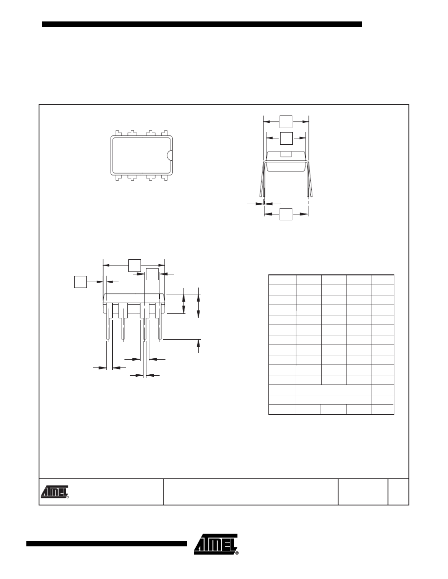
8-lead, 0.300" Wide, Plastic Dual Inline Package (PDIP)
8S2
8-lead, 0.209" Wide, Plastic Gull-Wing Small Outline (EIAJ SOIC)
S8S1
8-lead, 0.150" Wide, Plastic Gull-Wing Small Outline (JEDEC SOIC)
9
ATtiny13
2535CS–AVR–02/04
Packaging Information
8P3
2325 Orchard Parkway
San Jose, CA 95131
TITLE
DRAWING NO.
R
REV.
8P3, 8-lead, 0.300" Wide Body, Plastic Dual
In-line Package (PDIP)
01/09/02
8P3
B
D
D1
E
E1
e
L
b2
b
A2 A
1
N
eA
c
b3
4 PLCS
Top View
Side View
End View
COMMON DIMENSIONS
(Unit of Measure = inches)
SYMBOL
MIN
NOM
MAX
NOTE
Notes:
1. This drawing is for general information only; refer to JEDEC Drawing MS-001, Variation BA for additional information.
2. Dimensions A and L are measured with the package seated in JEDEC seating plane Gauge GS-3.
3. D, D1 and E1 dimensions do not include mold Flash or protrusions. Mold Flash or protrusions shall not exceed 0.010 inch.
4. E and eA measured with the leads constrained to be perpendicular to datum.
5. Pointed or rounded lead tips are preferred to ease insertion.
6. b2 and b3 maximum dimensions do not include Dambar protrusions. Dambar protrusions shall not exceed 0.010 (0.25 mm).
A
0.210
2
A2
0.115
0.130
0.195
b
0.014
0.018
0.022
5
b2
0.045
0.060
0.070
6
b3
0.030
0.039
0.045
6
c
0.008
0.010
0.014
D
0.355
0.365
0.400
3
D1
0.005
3
E
0.300
0.310
0.325
4
E1
0.240
0.250
0.280
3
e
0.100 BSC
eA
0.300 BSC
4
L
0.115
0.130
0.150
2
10
ATtiny13
2535CS–AVR–02/04
8S2
2325 Orchard Parkway
San Jose, CA 95131
TITLE
DRAWING NO.
R
REV.
8S2, 8-lead, 0.209" Body, Plastic Small
Outline Package (EIAJ)
10/7/03
8S2
C
COMMON DIMENSIONS
(Unit of Measure = mm)
SYMBOL
MIN
NOM
MAX
NOTE
Notes: 1. This drawing is for general information only; refer to EIAJ Drawing EDR-7320 for additional information.
2. Mismatch of the upper and lower dies and resin burrs are not included.
3. It is recommended that upper and lower cavities be equal. If they are different, the larger dimension shall be regarded.
4. Determines the true geometric position.
5. Values b and C apply to pb/Sn solder plated terminal. The standard thickness of the solder layer shall be 0.010 +0.010/
−0.005 mm.
A 1.70
2.16
A1 0.05
0.25
b
0.35
0.48 5
C
0.15
0.35 5
D 5.13
5.35
E1 5.18
5.40 2,
3
E 7.70
8.26
L 0.51
0.85
∅
0˚
8˚
e
1.27 BSC
4
End View
Side View
e
b
A
A1
D
E
N
1
C
E1
∅
L
Top View
11
ATtiny13
2535CS–AVR–02/04
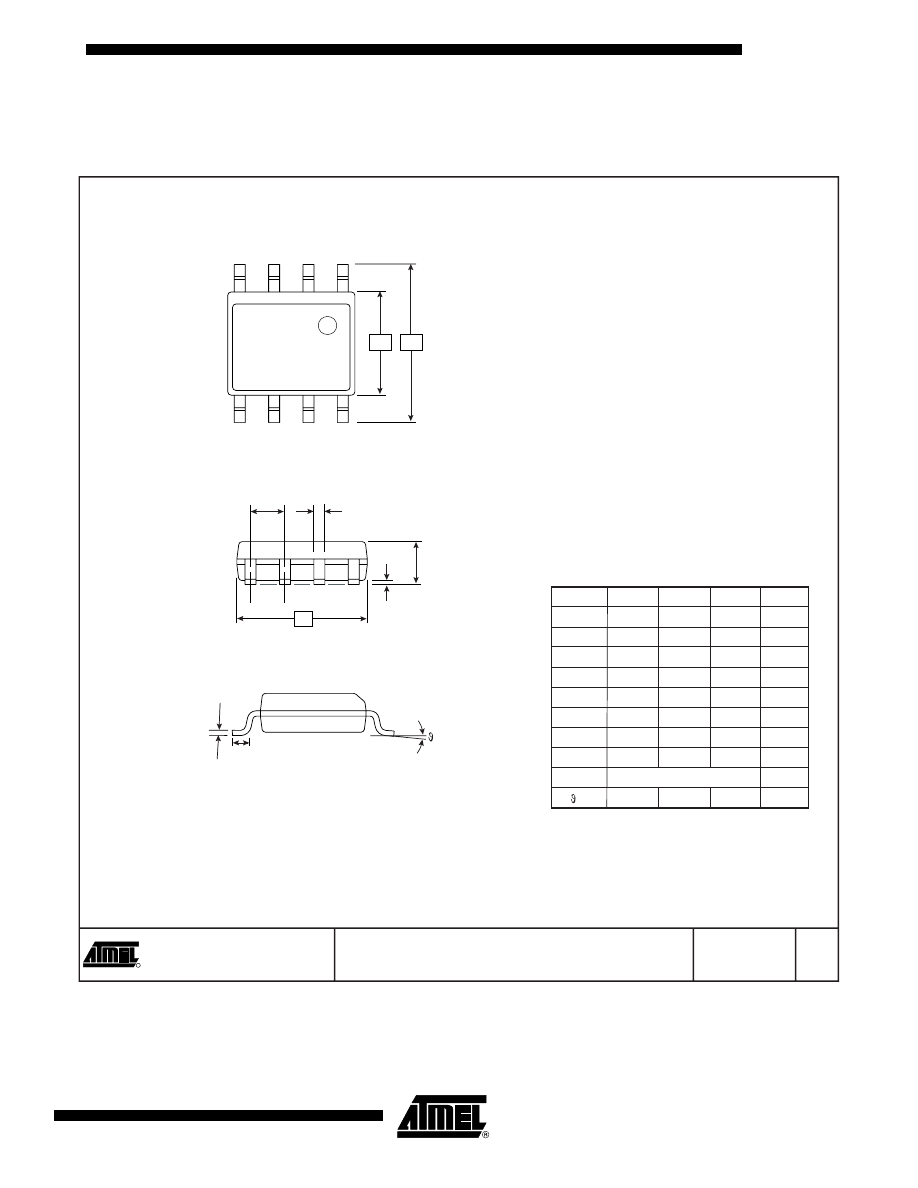
S8S1
2325 Orchard Parkway
San Jose, CA 95131
TITLE
DRAWING NO.
R
REV.
S8S1, 8-lead, 0.150" Wide Body, Plastic Gull Wing Small
Outline (JEDEC SOIC)
7/28/03
S8S1
A
COMMON DIMENSIONS
(Unit of Measure = mm)
SYMBOL
MIN
NOM
MAX
NOTE
Notes: 1. This drawing is for general information only; refer to JEDEC Drawing MS-012 for proper dimensions, tolerances, datums,etc.
E
5.79
6.20
E1
3.81
3.99
A
1.35
1.75
A1
0.1
0.25
D
4.80
4.98
C
0.17
0.25
b
0.31
0.51
L
0.4
1.27
e
1.27 BSC
0
o
8
o
Top View
Side View
End View
1
N
C
A
A1
b
L
e
D
E1
E

12
ATtiny13
2535CS–AVR–02/04
Errata
The revision letter in this section refers to the revision of the ATtiny13 device.
ATtiny13 Rev. B
•
Wrong values read after Erase Only operation
•
High Voltage Serial Programming Flash, EEPROM, Fuse and Lock Bits may fail
•
Device may lock for further programming
•
debugWIRE communication not blocked by lock-bits
•
Watchdog Timer Interrupt disabled
1.
Wrong values read after Erase Only operation
At supply voltages below 2.7 V, an EEPROM location that is erased by the Erase
Only operation may read as programmed (0x00).
Problem Fix/Workaround
If it is necessary to read an EEPROM location after Erase Only, use an Atomic Write
operation with 0xFF as data in order to erase a location. In any case, the Write Only
operation can be used as intended. Thus no special considerations are needed as
long as the erased location is not read before it is programmed.
2.
High Voltage Serial Programming Flash, EEPROM, Fuse and Lock Bits may
fail
Writing to any of these locations and bits may in some occasions fail.
Problem Fix/Workaround
After a writing has been initiated, always observe the RDY/BSY signal. If the writing
should fail, rewrite until the RDY/BSY verifies a correct writing. This will be fixed in
revision D.
3.
Device may lock for further programming
Special combinations of fuse bits will lock the device for further programming effec-
tively turning it into an OTP device. The following combinations of settings/fuse bits
will cause this effect:
–
128 kHz internal oscillator (CKSEL[1..0] = 11), shortest start-up time
(SUT[1..0] = 00), Debugwire enabled (DWEN = 0) or Reset disabled
RSTDISBL = 0.
–
9.6 MHz internal oscillator (CKSEL[1..0] = 10), shortest start-up time
(SUT[1..0] = 00), Debugwire enabled (DWEN = 0) or Reset disabled
RSTDISBL = 0.
–
4.8 MHz internal oscillator (CKSEL[1..0] = 01), shortest start-up time
(SUT[1..0] = 00), Debugwire enabled (DWEN = 0) or Reset disabled
RSTDISBL = 0.
Problem fix/ Workaround
Avoid the above fuse combinations. Selecting longer start-up time will eliminate the
problem.
4.
debugWIRE communication not blocked by lock-bits
When debugWIRE on-chip debug is enabled (DWEN = 0), the contents of program
memory and EEPROM data memory can be read even if the lock-bits are set to
block further reading of the device.
Problem fix/ Workaround
Do not ship products with on-chip debug of the tiny13 enabled.

13
ATtiny13
2535CS–AVR–02/04
5.
Watchdog Timer Interrupt disabled
If the watchdog timer interrupt flag is not cleared before a new timeout occurs, the
watchdog will be disabled, and the interrupt flag will automatically be cleared. This is
only applicable in interrupt only mode. If the Watchdog is configured to reset the
device in the watchdog time-out following an interrupt, the device works correctly.
Problem fix / Workaround
Make sure there is enough time to always service the first timeout event before a
new watchdog timeout occurs. This is done by selecting a long enough time-out
period.
ATtiny13 Rev. A
Revision A has not been sampled.

14
ATtiny13
2535CS–AVR–02/04
Datasheet Change
Log for ATtiny13
Please note that the referring page numbers in this section are referring to this docu-
ment. The referring revision in this section are referring to the document revision.
Changes from Rev.
2535B-01/04 to Rev.
2535C-02/04
Changes from Rev.
2535A-06/03 to Rev.
2535B-01/04
1.
C-code examples updated to use legal IAR syntax.
2.
Replaced occurences of WDIF with WDTIF and WDIE with WDTIE.
3.
Updated “Stack Pointer” on page 8.
4.
Updated “Calibrated Internal RC Oscillator” on page 22.
5.
Updated “Oscillator Calibration Register – OSCCAL” on page 22.
6.
Updated typo in introduction on “Watchdog Timer” on page 35.
7.
Updated “ADC Conversion Time” on page 82.
8.
Updated “Serial Downloading” on page 103.
9.
Updated “Electrical Characteristics” on page 115.
10.
Updated “Ordering Information” on page 8.
11.
Removed rev. C from “Errata” on page 12.
1.
Updated Figure 2 on page 2.
2.
Updated Table 12 on page 30, Table 17 on page 39, Table 37 on page 89
and Table 57 on page 116.
3.
Updated “Calibrated Internal RC Oscillator” on page 22.
4.
Updated the whole “Watchdog Timer” on page 35.
5.
Updated Figure 53 on page 103 and Figure 56 on page 108.
6.
Updated registers “MCU Control Register – MCUCR” on page 49,
“Timer/Counter Control Register B – TCCR0B” on page 69 and “Digital
Input Disable Register 0 – DIDR0” on page 76.
7.
Updated Absolute Maximum Ratings and DC Characteristics in “Electrical
Characteristics” on page 115.
8.
Added “Maximum Speed vs. VCC” on page 116
9.
Updated “ADC Characteristics – Preliminary Data” on page 118.
10.
Updated “ATtiny13 Typical Characteristics” on page 119.
11.
Updated “Ordering Information” on page 8.
12.
Updated “Packaging Information” on page 9.
13.
14.
Changed instances of EEAR to EEARL.

Printed on recycled paper.
Disclaimer: Atmel Corporation makes no warranty for the use of its products, other than those expressly contained in the Company’s standard
warranty which is detailed in Atmel’s Terms and Conditions located on the Company’s web site. The Company assumes no responsibility for any
errors which may appear in this document, reserves the right to change devices or specifications detailed herein at any time without notice, and
does not make any commitment to update the information contained herein. No licenses to patents or other intellectual property of Atmel are
granted by the Company in connection with the sale of Atmel products, expressly or by implication. Atmel’s products are not authorized for use
as critical components in life support devices or systems.
Atmel Corporation
Atmel Operations
2325 Orchard Parkway
San Jose, CA 95131, USA
Tel: 1(408) 441-0311
Fax: 1(408) 487-2600
Regional Headquarters
Europe
Atmel Sarl
Route des Arsenaux 41
Case Postale 80
CH-1705 Fribourg
Switzerland
Tel: (41) 26-426-5555
Fax: (41) 26-426-5500
Asia
Room 1219
Chinachem Golden Plaza
77 Mody Road Tsimshatsui
East Kowloon
Hong Kong
Tel: (852) 2721-9778
Fax: (852) 2722-1369
Japan
9F, Tonetsu Shinkawa Bldg.
1-24-8 Shinkawa
Chuo-ku, Tokyo 104-0033
Japan
Tel: (81) 3-3523-3551
Fax: (81) 3-3523-7581
Memory
2325 Orchard Parkway
San Jose, CA 95131, USA
Tel: 1(408) 441-0311
Fax: 1(408) 436-4314
Microcontrollers
2325 Orchard Parkway
San Jose, CA 95131, USA
Tel: 1(408) 441-0311
Fax: 1(408) 436-4314
La Chantrerie
BP 70602
44306 Nantes Cedex 3, France
Tel: (33) 2-40-18-18-18
Fax: (33) 2-40-18-19-60
ASIC/ASSP/Smart Cards
Zone Industrielle
13106 Rousset Cedex, France
Tel: (33) 4-42-53-60-00
Fax: (33) 4-42-53-60-01
1150 East Cheyenne Mtn. Blvd.
Colorado Springs, CO 80906, USA
Tel: 1(719) 576-3300
Fax: 1(719) 540-1759
Scottish Enterprise Technology Park
Maxwell Building
East Kilbride G75 0QR, Scotland
Tel: (44) 1355-803-000
Fax: (44) 1355-242-743
RF/Automotive
Theresienstrasse 2
Postfach 3535
74025 Heilbronn, Germany
Tel: (49) 71-31-67-0
Fax: (49) 71-31-67-2340
1150 East Cheyenne Mtn. Blvd.
Colorado Springs, CO 80906, USA
Tel: 1(719) 576-3300
Fax: 1(719) 540-1759
Biometrics/Imaging/Hi-Rel MPU/
High Speed Converters/RF Datacom
Avenue de Rochepleine
BP 123
38521 Saint-Egreve Cedex, France
Tel: (33) 4-76-58-30-00
Fax: (33) 4-76-58-34-80
Literature Requests
www.atmel.com/literature
2535CS–AVR–02/04
© Atmel Corporation 2004. All rights reserved. Atmel
®
and combinations thereof, AVR
®
, and AVR Studio
®
are the registered trademarks of
Atmel Corporation or its subsidiaries. Microsoft
®
, Windows
®
, Windows NT
®
, and Windows XP
®
are the registered trademarks of Microsoft Corpo-
ration. Other terms and product names may be the trademarks of others

This datasheet has been download from:
Datasheets for electronics components.
Document Outline
- Features
- Pin Configurations
- Overview
- Register Summary
- Instruction Set Summary
- Ordering Information
- Packaging Information
- Errata
- Datasheet Change Log for ATtiny13
Wyszukiwarka
Podobne podstrony:
Attiny 28L opis
N 13 opis(1)
Attiny 2313 opis
N 13 opis
dod 13 opis do projektu konstrukcji bochotnica
Ćwiczenie 13 - opis, Ćwiczenie 13
dod 13 opis do projektu konstrukcji bochotnica
Attiny 28L opis
Attiny 28L opis
opis budowl tbs 13 bud2 wykon i Nieznany
opis ark bad got szk 13
LAB 13 SSANIE OPIS, sgsp, Hydromechanika, HYDROMECHANIKA 1
13 35 Parking Focha Opis 1pazdzid 14598
Deplewski L AIUZE opis(1) id 13 Nieznany
więcej podobnych podstron