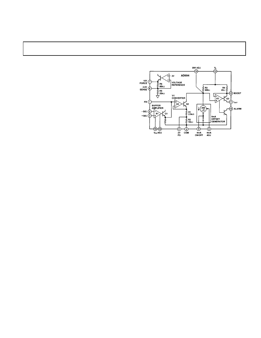
FUNCTIONAL BLOCK DIAGRAM
REV. A
Information furnished by Analog Devices is believed to be accurate and
reliable. However, no responsibility is assumed by Analog Devices for its
use, nor for any infringements of patents or other rights of third parties
which may result from its use. No license is granted by implication or
otherwise under any patent or patent rights of Analog Devices.
a
4–20 mA Transmitter
AD694*
FEATURES
4–20 mA, 0–20 mA Output Ranges
Precalibrated Input Ranges:
0 V to 2 V, 0 V to 10 V
Precision Voltage Reference
Programmable to 2.000 V or 10.000 V
Single or Dual Supply Operation
Wide Power Supply Range: +4.5 V to +36 V
Wide Output Compliance
Input Buffer Amplifier
Open-Loop Alarm
Optional External Pass Transistor to Reduce
Self-Heating Errors
0.002% typ Nonlinearity
PRODUCT DESCRIPTION
The AD694 is a monolithic current transmitter that accepts
high level signal inputs to drive a standard 4–20 mA current
loop for the control of valves, actuators, and other devices com-
monly used in process control. The input signal is buffered by
an input amplifier that can be used to scale the input signal or
buffer the output from a current mode DAC. Precalibrated in-
put spans of 0 V to 2 V and 0 V to 10 V are selected by simple
pin strapping; other spans may be programmed with external
resistor.
The output stage compliance extends to within 2 V of V
S
and its
special design allows the output voltage to extend below com-
mon in dual supply operation. An alarm warns of an open 4-to-
20 mA loop or noncompliance of the output stage.
Active laser trimming of the AD694’s thin film resistors results
in high levels of accuracy without the need for additional adjust-
ments and calibration. An external pass transistor may be used
with the AD694 to off-load power dissipation, extending the
temperature range of operation.
The AD694 is the ideal building block for systems requiring
noise immune 4–20 mA signal transmission to operate valves,
actuators, and other control devices, as well as for the transmis-
sion of process parameters such as pressure, temperature, or
flow. It is recommended as a replacement for discrete designs in
a variety of applications in industrial process control, factory
automation, and system monitoring.
The AD694 is available in hermetically sealed, 16-pin cerdip
and plastic SOIC, specified over the –40
°
C to +85
°
C industrial
temperature range, and in a 16-pin plastic DIP, specified over
the 0
°
C to +70
°
C temperature range.
*Protected by U.S. Patents: 30,586; 4,250,445; 4,857,862.
One Technology Way, P.O. Box 9106, Norwood, MA 02062-9106, U.S.A.
Tel: 617/329-4700
Fax: 617/326-8703
PRODUCT HIGHLIGHTS
1. The AD694 is a complete voltage in to 4–20 mA out current
transmitter.
2. Pin programmable input ranges are pre-calibrated at 0 V to
2 V and 0 V to 10 V.
3. The input amplifier may be configured to buffer and scale the
input voltage, or to serve as an output amplifier for current
output DACs.
4. The output voltage compliance extends to within 2 V of the
positive supply and below common. When operated with a
5 V supply, the output voltage compliance extends 30 V be-
low common.
5. The AD694 interfaces directly to 8-, 10-, and 12-bit single
supply CMOS and bipolar DACs.
6. The 4 mA zero current may be switched on and off with a
TTL control pin, allowing 0–20 mA operation.
7. An open collector alarm warns of loop failure due to open
wires or noncompliance of the output stage.
8. A monitored output is provided to drive an external pass
transistor. The feature off-loads power dissipation to extend
the temperature range of operation and minimize self-heating
error.

AD694–SPECIFICATIONS
Model
AD694JN/AQ/AR
AD694BQ/BR
Min
Typ
Max
Min
Typ
Max
Units
INPUT CHARACTERISTICS
Input Voltage Range
–0.2
V
S
–2.0 V
V
S
–2.5 V –0.2
V
S
–2.0 V
V
S
–2.5 V V
Input Bias Current
Either Input, T
MIN
to T
MAX
1.5
5
1.5
5
nA
Offset Current, T
MIN
to T
MAX
±
0.1
61
±
0.1
61
nA
Offset Current Drift
±
1.0
±
5.0
±
1.0
±
5.0
pA/
°
C
Input Impedance
5
5
M
Ω
OUTPUT CHARACTERISTICS
Operating Current Range
0
23
0
23
mA
Specified Performance
4
20
4
20
mA
Output Voltage Compliance
V
S
–36 V
V
S
–2 V
V
S
–36 V
V
S
–2 V
V
Output Impedance, 4–20 mA
40.0
50.0
40.0
50.0
M
Ω
Current Limit (@ 2
×
FS Overdrive
24
44
24
44
mA
Slew Rate
1.3
1.3
mA/
µ
s
SPAN AND ZERO ACCURACY
1
4 mA Offset Error @ 0 V Input
2
Error from 4.000 mA, 4 mA On
±
10
620
±
5
610
µ
A
Error from 0.000 mA, 4 mA Off
0
+10
+20
0
+5
+10
µ
A
T
MIN
to T
MAX
±
10
640
±
5
620
µ
A
vs. Supply (2 V Span/10 V Span)
0.3/0.05
0.8/0.4
0.3/0.05
0.8/0.4
µ
A/V
Trim Range, 4 mA Zero
2.0
4.8
2.0
4.8
mA
Span
Nominal Transfer Function
Input FS = 2 V
8.0
8.0
mA/V
Input FS = 10 V
1.6
1.6
mA/V
Transfer Function Error from Nom,
Input FS = 2 V, 10 V
±
0.1
60.3
±
0.05
60.15
% of Span
T
MIN
to T
MAX
±
0.002
±
0.005
±
0.001
60.0025 % of Span/
°
C
vs. Supply
±
0.001
60.005
±
0.001
60.005
% of Span/V
Nonlinearity
3
±
0.005
60.015
±
0.001
60.005
% of Span
4 mA On: Max Pin 9 Voltage
0.8
0.8
V
4 mA Off: Min Pin 9 Voltage
3.0
2.5
3.0
2.5
V
VOLTAGE REFERENCE
Output Voltage: 10 V Reference
9.960
10.000
10.040
9.980
10.000
10.020
V
Output Voltage: 2 V Reference
1.992
2.000
2.008
1.996
2.000
2.004
V
T
MIN
to T
MAX
4
30
50
20
30
ppm/
°
C
vs. Load, V
REF
= 2 V, 10 V
0.15
0.50
0.15
0.50
mV/mA
vs. Supply, V
REF
= 2 V, 10 V
±
0.001
60.005
±
0.001
60.005
%/V
Output Current
Source
5
5
mA
Sink
0.2
0.2
mA
ALARM CHARACTERISTICS
V
CE(SAT)
@ 2.5 mA
0.35
0.35
V
Leakage Current
61
61
µ
A
Alarm Pin Current (Pin 10)
20
20
mA
POWER REQUIREMENTS
Specified Performance
24
24
V
Operating Range
2 V FS, V
REF
= 2 V
4.5
36
4.5
36
V
2 V, 10 V FS, V
REF
= 2 V, 10 V
12.5
36
12.5
36
V
Quiescent Current, 4 mA Off
1.5
2.0
1.5
2.0
mA
TEMPERATURE RANGE
Specified Performance
5
AD694AQ/BQ/AR/BR –40
+85
–40
+85
°
C
AD694JN
0
+70
0
+70
°
C
Operating
AD694AQ/BQ/AR/BR –55
+125
–55
+125
°
C
AD694JN
–40
+85
–40
+85
°
C
(@ +25
8C, R
L
= 250
V and V
S
= +24 V, unless otherwise noted)
REV. A
–2–
Model
AD694JN/AQ/AR
AD694BQ/BR
Min
Typ
Max
Min
Typ
Max
Units
BUFFER AMPLIFIER
6
Input Offset Voltage
Initial Offset
±
150
6500
±
50
6500
µ
V
T
MIN
to T
MAX
±
2
±
3
±
2
±
3
µ
V/
°
C
vs. Supply
80
90
80
90
dB
vs. Common Mode
80
90
80
90
dB
Trim Range
62.5
±
4.0
62.5
±
4.0
mV
Frequency Response
Unity Gain, Small Signal
300
300
kHz
Input Voluge Noise (0.1 Hz to 10 Hz)
2
2
µ
V p-p
Open-Loop Gain
V
O
= +10 V, R
L
≥
10 k
Ω
50
50
V/mV
Output Voltage @ Pin 1, FB
1
Minimum Output Voltage
1.0
10
1.0
10
mV
Maximum Output Voltage
V
S
–2.5 V
V
S
–2 V
V
S
–2.5 V
V
S
–2 V
V
NOTES
1
The single supply op amps of the AD694, lacking pull down current, may not reach 0.000 V at their outputs. For this reason, span, offset, and nonlinearity are
specified with the input amplifiers operating in their linear range. The input voltage used for the tests is 5 mV to 2 V and 5 mV to 10 V for the two precalibrated
input ranges. Span and zero accuracy are tested with the buffer amplifier configured as a follower.
2
Offset at 4 mA out and 0 mA out are extrapolated to 0.000 V input from measurements made at 5 mV and at full scale. See Note 1.
3
Nonlinearity is specified as the maximum deviation of the output, as a % of span, from a straight line drawn through the endpoints of the transfer function.
4
Voltage reference drift guaranteed by the Box Method. The voltage reference output over temperature will fall inside of a box whose length is determined by the
temperature range and whose height is determined by the maximum temperature coefficient multiplied by the temperature span in degrees C.
5
Devices tested at these temperatures with a pass transistor. Allowable temperature range of operation is dependent upon internal power dissipation. Absolute
maximum junction and case temperature should not be exceeded. See section: “Power Dissipation Considerations.”
6
Buffer amplifier specs for reference. Buffer amplifier offset and drift already included in Span and Zero accuracy specs above.
Specifications subject to change without notice.
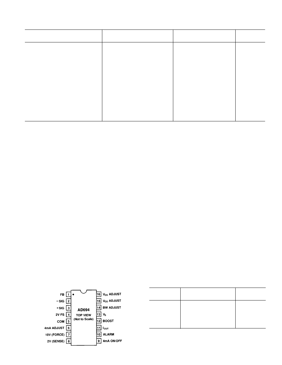
PIN CONFIGURATION (N, R, Q PACKAGE)
AD694
REV. A
–3–
ABSOLUTE MAXIMUM RATINGS
Supply Voltage . . . . . . . . . . . . . . . . . . . . . . . . . . . . . . . . +36 V
V
S
to I
OUT
. . . . . . . . . . . . . . . . . . . . . . . . . . . . . . . . . . . +36 V
Input Voltage, (Either Input Pin 2 or 3) . . . . . –0.3 V to +36 V
Reference Short Circuit to Common . . . . . . . . . . . . Indefinite
Alarm Voltage, Pin 10 . . . . . . . . . . . . . . . . . . . . . . . . . . +36 V
4 mA Adj, Pin 6 . . . . . . . . . . . . . . . . . . . . . . . . . . . . . . . . +1 V
4 mA On/Off, Pin 9 . . . . . . . . . . . . . . . . . . . . . . . . 0 V to 36 V
Storage Temperature Range
AD694Q . . . . . . . . . . . . . . . . . . . . . . . . . –65
°
C to +150
°
C
AD694N, R . . . . . . . . . . . . . . . . . . . . . . . –65
°
C to +125
°
C
Lead Temperature, 10 sec Soldering . . . . . . . . . . . . . . +300
°
C
Maximum Junction Temperature . . . . . . . . . . . . . . . . . +150
°
C
Maximum Case Temperature
Plastic Package (N, R) . . . . . . . . . . . . . . . . . . . . . . . +125
°
C
Cerdip Package (Q) . . . . . . . . . . . . . . . . . . . . . . . . . +125
°
C
No pin, other than I
OUT
(11) and
±
Sig (2), (3) as noted, may be permitted to become more negative than Com (5). No pin may be
permitted to become more positive than V
S
(13).
ORDERING GUIDE
Temperature
Package
Model
Range
Option*
AD694JN
0
°
C to +70
°
C
N-16
AD694AQ
–40
°
C to +85
°
C
Q-16
AD694AR
–40
°
C to +85
°
C
R-16
AD694BQ
–40
°
C to +85
°
C
Q-16
AD694BR
–40
°
C to +85
°
C
R-16
*N = Plastic DIP; Q = Cerdip, R = SOIC.
Transistor Count: . . . . . . . . . . . . . . . . . . . . .75 Active Devices
Substrate Connection: . . . . . . . . . . . . . . . . . . . . to Com, Pin 5
Thermal Characteristics:
Plastic (N) Package:
θ
JC
= 50
°
C/Watt
θ
CA
(Still Air) = 85
°
C/Watt
Cerdip (Q) Package:
θ
JC
= 30
°
C/Watt
θ
CA
(Still Air) = 70
°
C/Watt
Plastic (R) Package:
θ
JC
= 27
°
C/Watt
θ
CA
(Still Air) = 73
°
C/Watt
ESD Susceptibility
All pins are rated for a minimum of 4000 V protection, except
for Pins 2, 3 and 9 which are rated to survive a minimum of
1500 V. ESD testing conforms to Human Body Model. Always
practice ESD prevention.
AD694
–4–
REV. A
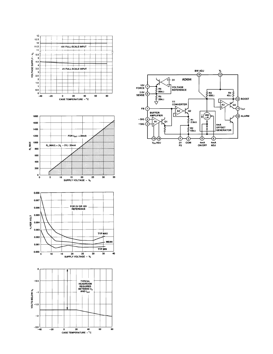
Typical Minimum Supply Voltage vs. Temperature for 2 V
& 10 V Full Scale
Maximum R
L
vs. Supply Voltage
Voltage Reference Power Supply Rejection
I
OUT
: Voltage Compliance vs. Temperature
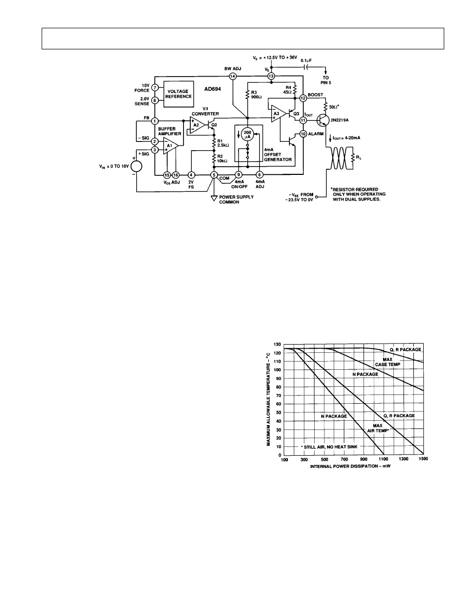
FUNCTIONAL DESCRIPTION
The operation of the AD694 can best be understood by dividing
the circuit into three functional parts (see Figure 1). First, a
single supply input amplifier buffers the high level, single-ended
input signal. The buffer amplifier drives the second section, a
voltage to current (V/I) converter, that makes a 0 to 16 mA sig-
nal dependent current.
Figure 1. Functional Block Diagram
The third section, a voltage reference and offset generator, is re-
sponsible for providing the 4 mA offset current signal.
BUFFER AMPLIFIER
The buffer amplifier is a single supply amplifier that may be
used as a unity gain buffer, an output amplifier for a current
output D/A converter, or as a gain block to amplify low level
signals. The amplifier’s PNP input stage has a common-mode
range that extends from a few hundred mV below ground to
within 2.5 V of V
S
. The Class A output of the amplifier appears
at Pin 1 (FB). The output range extends from about 1 mV
above common to within 2.5 V of V
S
when the amplifier is oper-
ated as a follower. The amplifier can source a maximum load of
5 k
Ω
, but can sink only as much as its internal 10 k
Ω
pulldown
resistor allows.
V/I CONVERTER
The ground referenced, input signal from the buffer amplifier is
converted to a 0 to 0.8 mA current by A2 and level shifted to
the positive supply. A current mirror then multiplies this signal
by a factor of 20 to make the signal current of 0 to 16 mA. This
technique allows the output stage to drive a load to within 2 V
of the positive supply (V
S
). Amplifier A2 forces the voltage at
Pin 1 across resistors R1 and R2 by driving the Darlington tran-
sistor, Q2. The high gain Darlington transmits the resistor cur-
rent to its collector and to R3 (900
Ω
). A3 forces the level
shifted signal across the 45
Ω
resistor to get a current gain of 20.
The transfer function of the V/I stage is therefore:
I
OUT
=
20
×
V
PIN1
(
)
/ R1
+
R2
(
)
resulting in a 0-16 mA output swing for a 0–10 V input. Tying
Pin 4 (2 V FS) to ground shorts out R2 and results in a 2 V
full-scale input for a 16 mA output span.
The output stage of the V/I converter is of a unique design that
allows the I
OUT
pin to drive a load below the common (sub-
strate) potential of the device. The output transistor can always
AD694
REV. A
–5–
Table I. Precalibrated Ranges for the AD694
I
nput
Output
Voltage
Min
Range
Range
Reference V
S
Pin 9
Pin 4
Pin 8
0–2 V
4–20 mA
2 V
4.5 V
Pin 5
Pin 5
Pin 7
0–10 V
4–20 mA
2 V
12.5 V
Pin 5
Open
Pin 7
0–2.5 V
0–20 mA
2 V
5.0 V
≥
3 V
Pin 5
Pin 7
0–12.5 V
0–20 mA
2 V
15.0 V
≥
3 V
Open
Pin 7
0–2 V
4–20 mA
10 V
12.5 V
Pin 5
Pin 5
Open
0–10 V
4–20 mA
10 V
12.5 V
Pin 5
Open
Open
0–2.5 V
0–20 mA
10 V
12.5 V
≥
3 V
Pin 5
Open
0–12.5 V
0–20 mA
10 V
15.0 V
≥
3 V
Open
Open
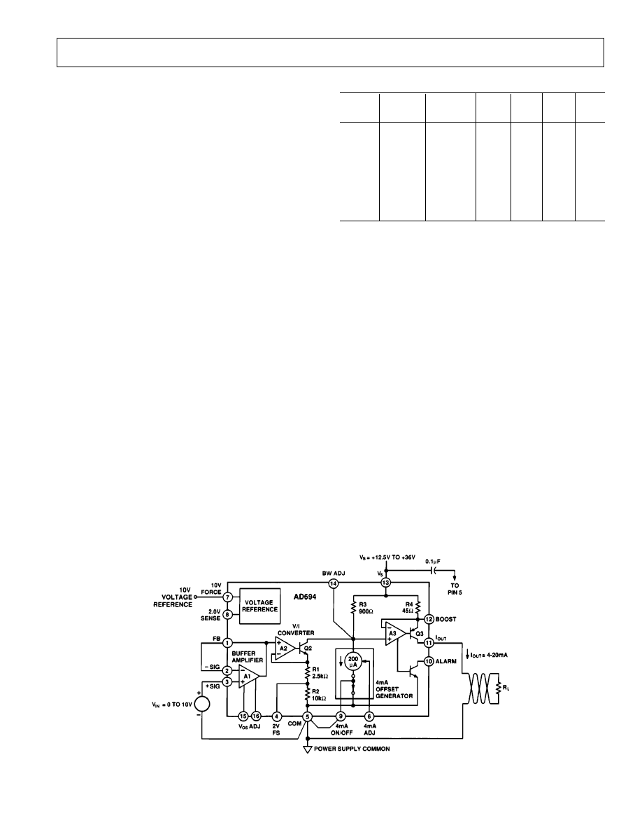
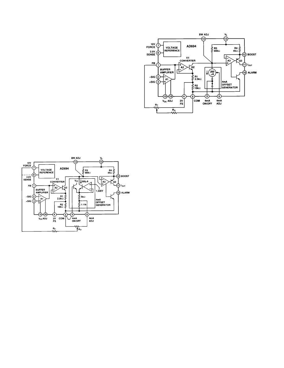
BASIC CONNECTIONS: 12.5 V SINGLE SUPPLY
OPERATION WITH 10 V FS
Figure 2 shows the minimal connections required for basic op-
eration with a +12.5 V power supply, 10 V input span, 4-20 mA
output span, and a 10 V voltage reference. The buffer amplifier
is connected as a voltage follower to drive the V/I converter by
connecting FB (Pin 1) to –Sig (Pin 2). 4 mA On/Off (Pin 9) is
tied to ground (Pin 5) to enable the 4 mA offset current. The
AD694 can drive a maximum load R
L
= [V
S
– 2 V] /20 mA,
thus the maximum load with a 12.5 V supply is 525
Ω
.
SELECTING A 2 V FULL-SCALE INPUT
The 2 V full-scale option is selected by shorting Pin 4 (2 V FS)
to Pin 5 (Common). The connection should be as short as pos-
sible; any parasitic resistance will affect the precalibrated span
accuracy.
SELECTING THE 2 V VOLTAGE REFERENCE
The voltage reference is set to a 2 V output by shorting Pin 7 to
Pin 8 (10 V Force to 2 V Sense). If desired, the 2 V reference
can be set up for remote force and sense connection. Keep in
mind that the 2 V Sense line carries a constant current of 100
µ
A
that could cause an offset error over long wire runs. The 2 V
reference option can be used with all supply voltages greater
than 4.5 V.
drive a load to a point 36 V below the positive supply (V
S
). An
optional NPN pass transistor can be added to transfer most of
the power dissipation off-chip, to extend the temperature range
of operation.
The output stage is current-limited at approximately 38 mA to
protect the output from an overdrive at its inputs. The V/I will
allow linear operation to approximately 24 mA. The V/I con-
verter also has an open collector alarm (Pin 10) which warns of
open-circuit condition at the I
OUT
pin or of attempts to drive the
output to a voltage greater than V
S
–2 V.
4 mA OFFSET GENERATOR
This circuit converts a constant voltage from the voltage refer-
ence to a constant current of approximately 200
µ
A. This cur-
rent is summed with the signal current at Pin 14 (BW Adjust),
to result in a constant 4 mA offset current at I
OUT
. The 4 mA
Adj (Pin 6) allows the offset current to be adjusted to any cur-
rent in the range of 2 mA to 4.8 mA. Pin 9 (4 mA On/Off) can
shut off the offset current completely if it is lifted to 3.0 V or
more, allowing 0 to 20 mA operation of the AD694. In normal
4-20 mA operation, Pin 9 is connected to ground.
VOLTAGE REFERENCE
A 2 V or 10 V voltage reference is available for user applications,
selectable by pin-strapping. The 10 V option is available for
supply voltages greater than 12.5 V, the 2 V output is available
over the whole 4.5 V – 36 V power supply range. The reference
can source up to 5 mA for user applications. A boost transistor
can be added to increase the current drive capability of the 2 V
mode.
APPLYING THE AD694
The AD694 can easily be connected for either dual or single
supply operation, to operate from supplies as low as 4.5 V and
as high as 36 V. The following sections describe the different
connection configurations, as well as adjustment methods.
Table I shows possible connection options.
Figure 2. Minimal Connections for 0-10 V Single-Ended Input, 4-20 mA Output, 10 V Reference Output
AD694
–6–
REV. A
An NPN boost transistor can be added in the 2 V mode to in-
crease the current drive capability of the 2 V reference. The
10 V force pin is connected to the base of the NPN, and the
NPN emitter is connected to the 2 V sense pin. The minimum
V
S
Of the part increases by approximately 0.7 V.
4.5 V SINGLE SUPPLY OPERATION
For operation with a +4.5 V power supply, the input span and
the voltage reference output must be reduced to give the ampli-
fiers their required 2.5 V of head room for operation. This is
done by adjusting the AD694 for 2 V full-scale input, and a
voltage reference output of 2 V as described above.
GENERAL DESIGN GUIDELINES
A 0.1
µ
F decoupling capacitor is recommended in all applica-
tions from V
S
(Pin 13) to Com (Pin 5). Additional components
may be required if the output load is nonresistive, see section on
driving nonresistive loads. The buffer amplifier PNP inputs
should not be brought more than –0.3 V of common, or they
will begin to source large amounts of current. Input protection
resistors must be added to the inputs if there is a danger of this
occurring. The output of the buffer amplifier, Pin 1 (FB), is not
short circuit protected. Shorting this pin to ground or V
S
with a
signal present on the amplifier may damage it. Input signals
should not drive Pin 1 (FB) directly; always use the buffer am-
plifier to buffer input signals.
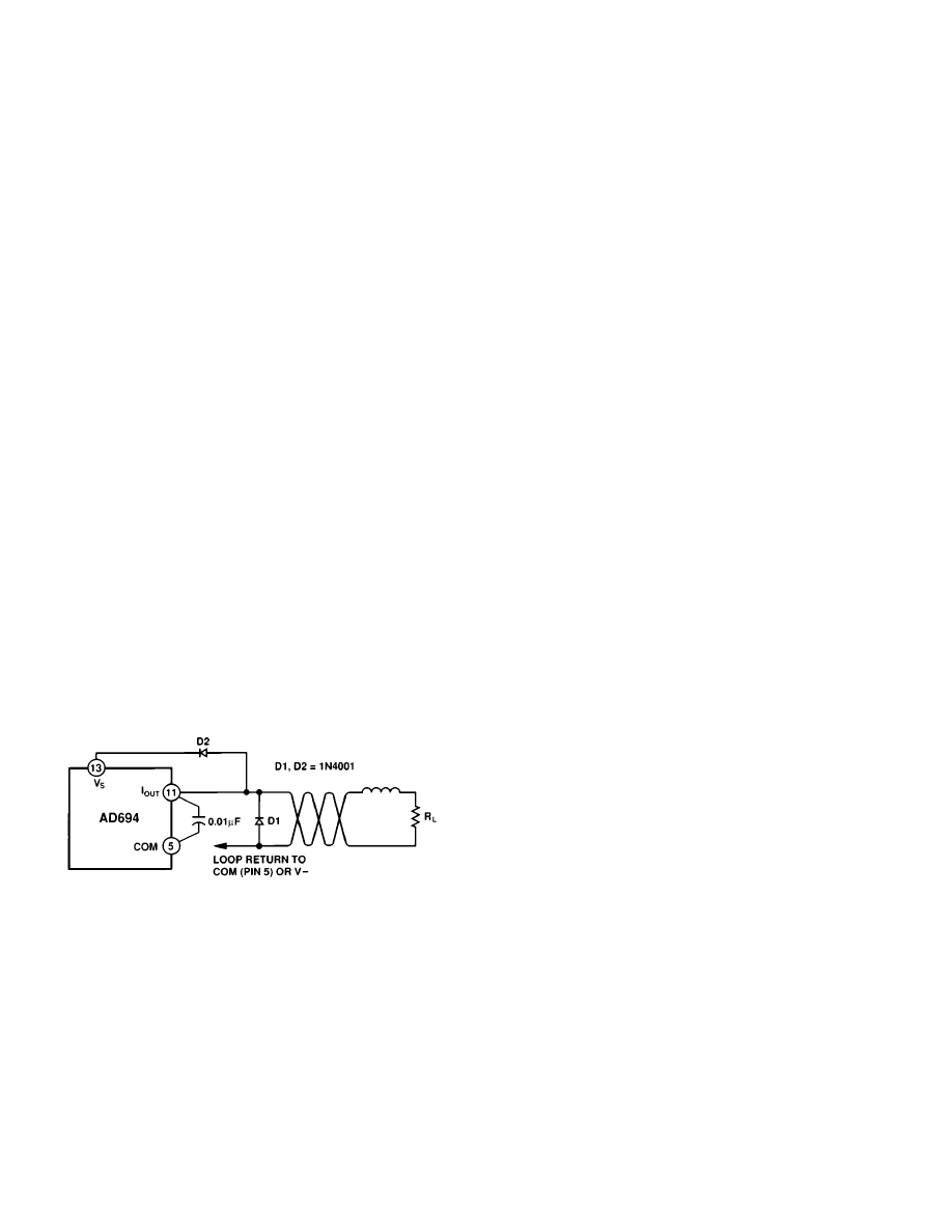
DRIVING NONRESISTIVE LOADS
The AD694 is designed to be stable when driving resistive loads.
Adding a 0.01
µ
F capacitor from I
OUT
(Pin 11) to Com (Pin 5),
as shown in Figure 3, insures the stability of the AD694 when
driving inductive or poorly defined loads. This capacitor is rec-
ommended when there is any uncertainty as to the characteris-
tics of the load.
Figure 3. Capacitor Utilized When Driving Nonresistive
Loads; Protection Diodes Used When Driving Inductive
Loads
Additional protection is recommended when driving inductive
loads. Figure 3 shows two protective diodes, D1 and D2, added
to protect against voltage spikes that may extend above V
S
or
below common that could damage the AD694. These diodes
should be used in addition to the 0.01
µ
F capacitor. When the
optional NPN transistor is used, the capacitor and diodes
should connect to the NPN emitter instead of Pin 11.
0-20 mA OPERATION
A 0-20 mA output range is available with the AD694 by remov-
ing the 4 mA offset current with the 4 mA On/Off pin. In nor-
mal 4-20 mA operation 4 mA On/Off (Pin 9) is tied to ground,
enabling the 4 mA offset current. Tying Pin 9 to a potential of
3 V or greater turns off the 4 mA offset current; connecting Pin
9 to the 10 V reference, the positive supply, or a TTL control
pin, is a convenient way to do this. In 0–20 mA mode the input
span is increased by 20%, thus the precalibrated input spans of
2 V and 10 V become 2.5 V and 12.5 V. Minimum supply volt-
ages for the two spans increase to 5 V and 15 V.
The 4 mA On/Off pin may also be used as a “jiggle pin” to
unstick valves or actuators, or as a way to shut off a 4–20 mA
loop entirely. Note that the pin only removes the 4 mA offset
and not the signal current.
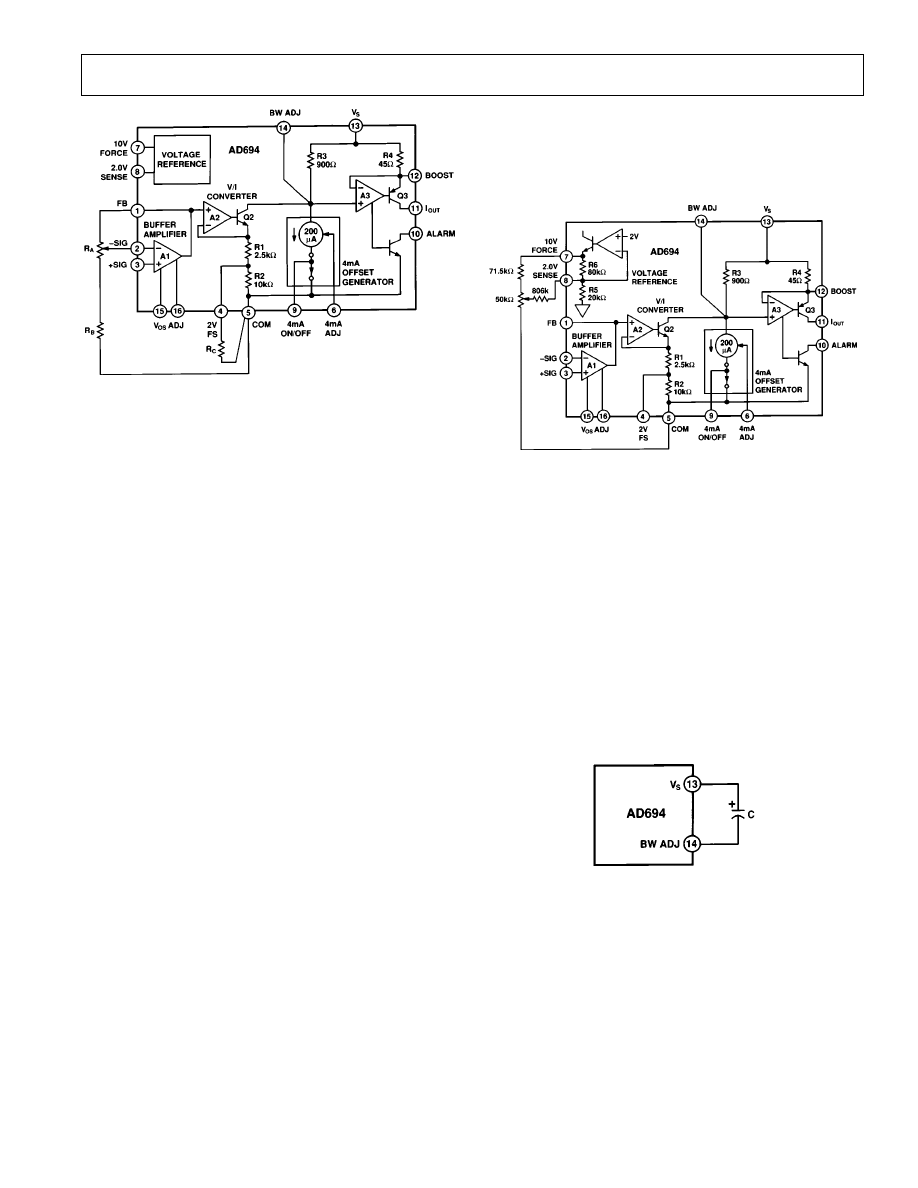
DUAL SUPPLY OPERATION
Figure 4 shows the AD694 operated in dual supply mode. (Note
that the pass transistor is shown for illustration and is not re-
quired for dual supply operation.) The device is powered com-
pletely by the positive supply which may be as low as 4.5 V. The
unique design of the output stage allows the I
OUT
pin to extend
below common to a negative supply. The output stage can
source a current to a point 36 V below the positive supply. For
example, when operated with a +12.5 V supply, the AD694 can
source a current to a point as low as 23.5 V below common.
This feature can simplify the interface to dual supply D/A con-
verters by eliminating grounding and level-shifting problems
while increasing the load that the transmitter is able to drive.
Note that the I
OUT
pin is the only pin that should be allowed to
extend lower than –0.3 V of common.
OPERATION WITH A PASS TRANSISTOR
The AD694 can operate as a stand-alone 4–20 mA converter
with no additional active components. However, provisions have
been made to connect I
OUT
to the base of an external NPN pass
transistor as shown in Figure 4. This permits a majority of the
power dissipation to be moved off-chip to enhance performance
and extend the temperature range of operation. Note that the
positive output voltage compliance is reduced by approximately
0.7 V, the V
BE
of the pass device. A 50
Ω
resistor should be
added in series with the pass transistor collector, when the
AD694 is operated with dual supplies, as shown in Figure 4.
This will not reduce the voltage compliance of the output stage.
The external pass transistor selected should have a BV
CEO
greater than the intended supply voltage with a sufficient power
rating for continuous operation with 25 mA current at the sup-
ply voltage. Ft should be in the 10 MHz to 100 MHz range and
β
should be greater than 10 at a 20 mA emitter current. Heat
sinking the external pass transistor is suggested.
AD694
REV. A
–7–
Figure 4. Using Optional Pass Transistor to Minimize Self-Heating Errors; Dual Supply Operation Shown
POWER DISSIPATION CONSIDERATIONS
The AD694 is rated for operation over its specified temperature
without the use of an external pass transistor. However, it is
possible to exceed the absolute maximum power dissipation,
with some combinations of power supply voltage and voltage
reference load. The internal dissipation of the part can be calcu-
lated to determine if there is a chance that the absolute maxi-
mum dissipation may be exceeded. The die temperature must
never exceed 150
°
C.
Total power dissipation (P
TOT
), is the sum of power dissipated
by the internal amplifiers, P (Standing), the voltage reference,
P(V
REF
) and the current output stage, P(I
OUT
) as follows:
P
TOT
= P (Standing) + P (V
REF
) + P (I
OUT
)
where:
P (Standing) = 2 mA (max)
×
V
S
P (V
REF
) = (V
S
– V
REF
)
×
I
VREF
P(I
OUT
) (V
S
– V
OUT
)
×
I
OUT
(max):
I
OUT
(max) may be the max expected operating cur-
rent, or the overdriven current of the device.
P(I
OUT
) drops to (2 Volts
×
I
OUT
) if a pass transistor
is used.
Definitions:
V
REF
= output voltage of reference
I
VREF
= output current of reference
V
S
= supply voltage
V
OUT
= voltage at I
OUT
pin.
An appropriate safety factor should be added to P
TOT
.
The junction temperature may be calculated with the following
formula:
T
J
= P
TOT
(
θ
JC
+
θ
CA
) + T
AMBIENT
θ
JC
is the thermal resistance between the chip and the package
(case),
θ
CA
is the thermal resistance between the case and its
surroundings and is determined by the characteristics of the
thermal connection of the case to ambient.
For example, assume that the part is operating with a V
S
of 24 V
in the cerdip package at 50
°
C, with a 1 mA load on the 10 V
reference. Assume that I
OUT
is grounded and that the max I
OUT
would be 20 mA. The internal dissipation would be:
P(
TOT
) = 2 mA
×
24 V + (24 V – 10 V)
×
1 mA + (24 V – 0 V)
×
20 mA
= 48 mW + 14 mW + 480 mW = 542 mW
Using
θ
JC
of 30
°
C/Watt and
θ
CA
of 70
°
C/Watt, (from spec page)
the junction temperature is:
T
J
= 542 mW (30
°
C/W + 70
°
C/W) + 50
°
C = 104.2
°
C
The junction temperature is in the safe region.
Internal power dissipation can be reduced either by reducing the
value of
θ
CA
through the use of air flow or heat sinks, or by re-
ducing P(
TOT
) of the AD694 through the use of an external pass
transistor. Figure 5 shows the maximum case and still air tem-
peratures for a given level of power dissipation.
Figure 5. Internal Power Dissipation in mW
ADJUSTMENT PROCEDURES
The following sections describe methods for trimming the out-
put current offset, the span and the voltage reference.
ADJUSTING 4 mA ZERO
The 4 mA zero current may be adjusted over the range of 2 mA
to 4.8 mA to accommodate large input signal offsets, or to allow
small adjustment in the zero current. The zero may be adjusted
by pulling up or down on Pin 6 (4 mA Adj) to increase or de-
crease the nominal offset current. The 4 mA Adj. (Pin 6) should
not be driven to a voltage greater than 1 V. The arrangement of
AD694
–8–
REV. A
Figure 6 will give an approximately linear adjustment of the
4 mA offset within fixed limits. To find the proper resistor val-
ues, first select X, the desired range of adjustment as a fraction
of 4 mA. Substitute this value in the appropriate formula below
along with the chosen reference output voltage (V
REF
= 2 V or
10 V usually), to determine the resistor values required.
R
P
= 180
Ω
(1/X – 4.5)
R
F
= 500
Ω
[(V
REF
/ 1.22 V) – 0.18 – 0.82X][1/X – 4.5]
These formulae take into account the
±
10% internal resistor
tolerance and ensure a minimum adjustment range for the 4 mA
offset. For example, assume the 2 V reference option has been
selected. Choosing X = 0.05; gives an adjustment range of
±
5%
of the 4 mA offset.
R
P
= 180
Ω
(1/0.05 – 4.5) = 2.79 k
Ω
R
F
= 500
Ω
[(2 V / 1.22) – 0.18 – 0.82
×
0.05][1/0.05 – 4.5]
= 10.99 k
Ω
These can be rounded down to more convenient values of
2.5 k
Ω
and 9.76 k
Ω
. In general, if the value of R
P
is rounded
down slightly, the value of R
F
should be rounded down propor-
tionately and vice versa. This helps to keep the adjustment range
symmetrical.
Figure 6. Optional 4 mA Zero Adjustment
ADJUSTING SPAN FOR 10 V FS
When the AD694 is configured with a 10 V input full-scale the
span maybe adjusted using the network shown in Figure 7. This
scheme allows an approximately linear adjustment of the span
above or below the nominal value. The span adjustment does
not interact with the 4 mA offset. To select R
S
and R
T
), choose
Figure 7. Span Adjustment, 10 V Full Scale
X, the desired adjustment range as a fraction of the span. Sub-
stitute this value in the appropriate formula below.
R
T
= 1.8 k
Ω
((1 – X)/X)
R
S
= 9 k
Ω
[1 – 0.2 (1 + X)( 1 – X )] / 2X
These formulae take into account the
±
10% absolute resistor
tolerance of the internal span resistors and ensures a minimum
adjustment range of the span. For example, choosing the adjust-
ment range to be
±
2%, or 0.02 gives:
R
T
= 1.8 k
Ω
((1 – 0.02) / 0.02) = 88.2 k
Ω
.
R
S
= 9 k
Ω
[1 – 0.2 (1 + 0.02)( 1 – 0.02 )] / (2
×
0.02) =
175.5 k
Ω
These values can be rounded up to the more convenient values
of 100 k
Ω
and 198 k
Ω
. In general, if R
T
is rounded up, then the
value of R
S
should be rounded up proportionally and vice versa.
ADJUSTING SPAN FOR 2 V FS
The precalibrated 2 V full-scale range requires a different ad-
justment scheme due to the single supply nature of the AD694.
Figure 8 shows an adjustment scheme that allows an approxi-
mately linear adjustment of the 2 V span plus or minus the
nominal value. The span adjustment does not affect the value of
the 4 mA offset current.
To find the proper resistor values first select X, the desired
range of adjustment as a fraction of the output span. Substitute
this value into the following formulae:
R
A
= 2
×
X
×
R
B
where R
B
is greater than 5 K
R
C
= (2.75 k
Ω
×
X)/(1 – 0.275X)
These formulae take into account the
±
10% absolute tolerance
of the internal span resistors and ensure a minimum adjustment
range.
For example, choosing the adjustment range to be
±
320
µ
A of
FS or,
±
2%, let X = 0.02. Thus:
Setting R
B
= 10 K, then R
A
= 2(.02)
×
10 k
Ω
= 400
Ω
R
C
= (2.75 k
Ω
×
0.02)/ (1 – 0.275
×
(0.02)) = 55.3
Ω
The value of R
C
can be rounded to the more convenient values
of 49.9
Ω
. In general, if R
A
is rounded up, then R
C
should be
rounded up proportionally and vice versa; rounding up will in-
crease the range of adjustment.
AD694
REV. A
–9–
Figure 8. Span Adjustment, 2 V Full Scale
PROGRAMMING OTHER SPANS
There are two methods for programming input spans less than
10 V. The first decreases the input span by programming a non-
inverting gain into the buffer amplifier. For example, to achieve
an input span of 0–5 V, the AD694 is set in its 10 V full-scale
mode and the buffer amplifier is configured with a noninverting
gain of 2 by adding 2 resistors. Now a 5 V signal at +Sig results
in a 10 V full-scale signal at FB (Pin 1), the input to the V/I.
This method requires that the V/I be programmed to a 10 V full
scale for input spans between 2 V to 10 V. It should be pro-
grammed to a 2 V full scale if input spans of less than 2 V are
required. This adjustment scheme makes the accuracy of the
span adjustment dependent upon the ratio accuracy of the re-
quired gain resistors. Thus, it is possible to accurately configure
spans other than 2 V or 10 V without using trimming potenti-
ometers, given that the resistor ratios are sufficiently accurate. A
supply voltage of 12.5 V is required for spans between 2 V and
10 V. Spans below 2 V require a V
S
of 4.5 V or greater.
A second method, allows other spans of less than 10 V to be
programmed when supply voltage is less than 12.5 V. Since the
AD694 amplifiers require 2.5 V of headroom for operation, a
5 V full-scale input is possible with a 7.5 V supply. This is
achieved by placing a resistor, in parallel with R2, (2 V FS (Pin
4) to Com (Pin 5)), to adjust the transconductance of the V/I
converter without a headroom penalty. A disadvantage of this
method is that the external resistor must match the internal re-
sistor in a precise manner, thus a span trim will be required.
The value should be chosen to allow for the
±
10% uncertainty
in the absolute value of the internal resistor R2.
ADJUSTING REFERENCE OUTPUT
Figure 9 shows one method of making small adjustments to the
10 V reference output. This circuit allows a linear adjustment
range of
±
200 mV. The 2 V reference may also be adjusted but
only in the positive direction.
Other reference voltages can be programmed by adding external
resistors. For example, a resistor placed in parallel with R5 can
be added to boost the reference output as high as 20 V. Con-
versely, a resistor in parallel with R6 can be used to set the refer-
ence voltage to a value between 2 V and 10 V. The output
voltage V
REF
= 2 V (R6 + R5) / R5. In choosing external
adjustment resistors remember that the internal resistors, while
ratio matched to a high degree of accuracy, have an absolute re-
sistor tolerance of only
±
10%. Be prepared to compensate for
this if a precise voltage other than the precalibrated values of 2
V or 10 V is required.
Figure 9. 10 V Reference Output Adjustment
BANDWIDTH CONTROL
The bandwidth of the AD694 can be limited to provide noise
filtering. This is achieved by connecting an external capacitor
from BW ADJ (Pin 14) to V
S
(Pin 13) as shown in Figure 10.
To program the bandwidth, substitute the desired bandwidth in
Hz, into the formula below to determine the required capacitor.
C = 1 farad Hz
Ω
/(2
π
900
Ω
BW)
The bandwidth chosen will vary
±
10% due to internal resistor
tolerance, plus an additional amount due to capacitor tolerance.
This method of bandwidth control is not recommended as a
way to filter large high frequency transients in the input signal.
It is recommended that frequencies greater than the BW of the
buffer amplifier be eliminated with an input filter to avoid recti-
fication of noise by the input amplifiers.
Figure 10. Noise Filtering with an External Capacitor
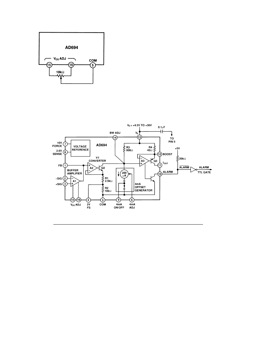
BUFFER AMPLIFIER OFFSET ADJUST
The buffer amplifier input voltage offset has been laser trimmed
to a high degree of accuracy; however, there may be occasions
when an offset trim is desired. Figure 11 shows the adjustment
method; a trim range of greater than
±
2.5 mV is available with
this scheme. It is not recommended that this adjustment
method be used to affect the 4 mA offset current as the trim will
induce offset drift into the buffer amplifier. The buffer amplifier
will drift approximately 1
µ
V/
°
C for each 300
µ
V of induced
offset. To adjust the 4 mA offset current refer to the section
“ADJUSTING ZERO.”
AD694
–10–
REV. A
Figure 11. Buffer Amplifier V
OS
Adjustment
APPLICATIONS
CURRENT OUTPUT DAC INTERFACE
The AD694 can be easily interfaced to current output DACs
such as the AD566A to construct a digital to 4–20 mA interface
as shown in Figure 13. The AD694 provides the voltage refer-
ence and the buffer amplifier necessary to operate the DAC.
Only simple connections are necessary to construct the circuit.
The 10 V reference of the AD694 supplies reference input of the
AD566. The buffer amplifier converts the full-scale current to
+10 V utilizing the internal resistors in the DAC; therefore the
AD694 is configured for a 10 V full-scale input. A 10 pF capaci-
tor compensates for the 25 pF output capacitance of the DAC.
An optional 100
Ω
trim resistor, (R
T
), allows the full-scale to be
trimmed, a 50
Ω
resistor may be substituted if a trim is not re-
quired; accuracy will be typically
±
1 LSB and the trim does not
affect the 4 mA offset. Care should be taken in managing the
circuit grounds. Connections from AD694 Pins 9, 3 and AD566
Pins 3 and 7 should be as short as possible and to a single point
close to Pin 5 of the AD694. Best practice would have separate
connections to the star ground from each pin; this is essential
Figure 12. Using the Alarm to Drive a TTL Gate
ALARM CIRCUIT
The AD694 has an alarm circuit which warns of open circuit
conditions at I
OUT
(Pin 11), or of attempts to drive the voltage
at I
OUT
higher than V
S
– 2 V. The alarm transistor will pull
down if an out of control condition is sensed. The alarm current
is limited to about 20 mA.
Figure 12 shows a typical application. In a digital/analog system
the alarm can provide a TTL signal to a controller. The collec-
tor of the alarm transistor is tied to the system logic supply
through a 20 k
Ω
pull-up resistor. The alarm is off in normal op-
eration and the voltage at the alarm pin is high. In the event that
the wire from I
OUT
(Pin 11) is opened, or if a large input over-
drive forces I
OUT
too close to V
S
, then the alarm pin is driven
low. This configuration is compatible with CMOS or TTL logic
levels. The alarm transistor can also be used to directly drive an
LED or other indicators.
for the AD566 power ground from Pin 12. The 4–20 mA output
(Pin 11) must have a return path to the power ground. The re-
turn line from the load may be connected to the power ground,
or to the –15 V supply based upon the size of the load to be
driven, and on power dissipation considerations.
SINGLE SUPPLY DIGITAL TO 4–20 mA INTERFACE
A 12 bit input to 4–20 mA output interface can be constructed
that operates on a single 15 V supply. The DAC is operated in
its voltage switching mode; this allows the DAC, when supplied
with a voltage reference of less than 2.5 V, to provide an output
voltage that is proportional to the digital input code and ranges
from 0 V to V
REF
. The AD694 voltage reference is connected to
supply 2 V and the input stage is set to a 2 V full scale; the input
buffer amplifier serves to buffer the voltage output from the
DAC. Connected in this manner a full-scale DAC input code
will result in a 20 mA output and an all 0 code will result in a
4 mA output. The loading on the AD694 voltage reference is
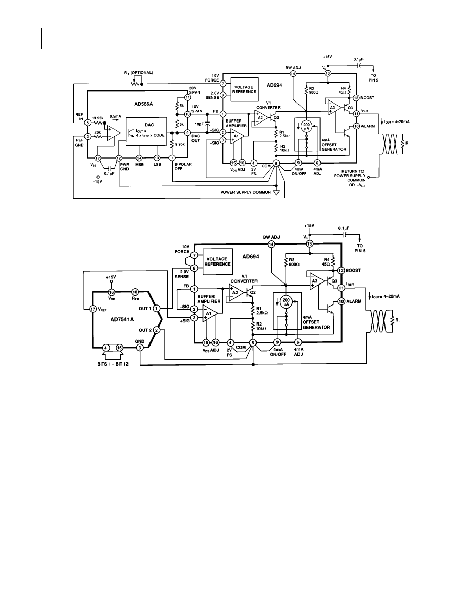
AD694
REV. A
–11–
Figure 13. Digital to 4–20 mA Interface Using a Current Steering DAC
Figure 14. Single Supply Digital Input to 4–20 mA Output
code dependent, and the response time of the circuit will be de-
termined by the reaction of the voltage reference. The supply
voltage to the AD7541A should be kept close to 15 V. If V
S
is
reduced significantly from 15 V the differential nonlinearity of
the DAC will increase and the linearity will be degraded.
In some applications it is desirable to have some under-range
and overrange in the 4–20 mA output. For example, assume an
over and under range capability of
±
5% of span is needed, then
the output current range corresponding to the full scale of the
DAC is 3.2 mA to 20.8 mA. To accomplish this, the span of the
AD694 would be increased 10% to 17.6 mA by adding a nonin-
verting gain of 1.1 to the buffer amplifier. The 4 mA offset
would then be reduced by 0.8 mA, by utilizing the adjustment
scheme explained in “Adjusting 4 mA Zero.” Then a digital in-
put from all zero code to full scale would result in an output
current of 3.2 mA to 20.8 mA.
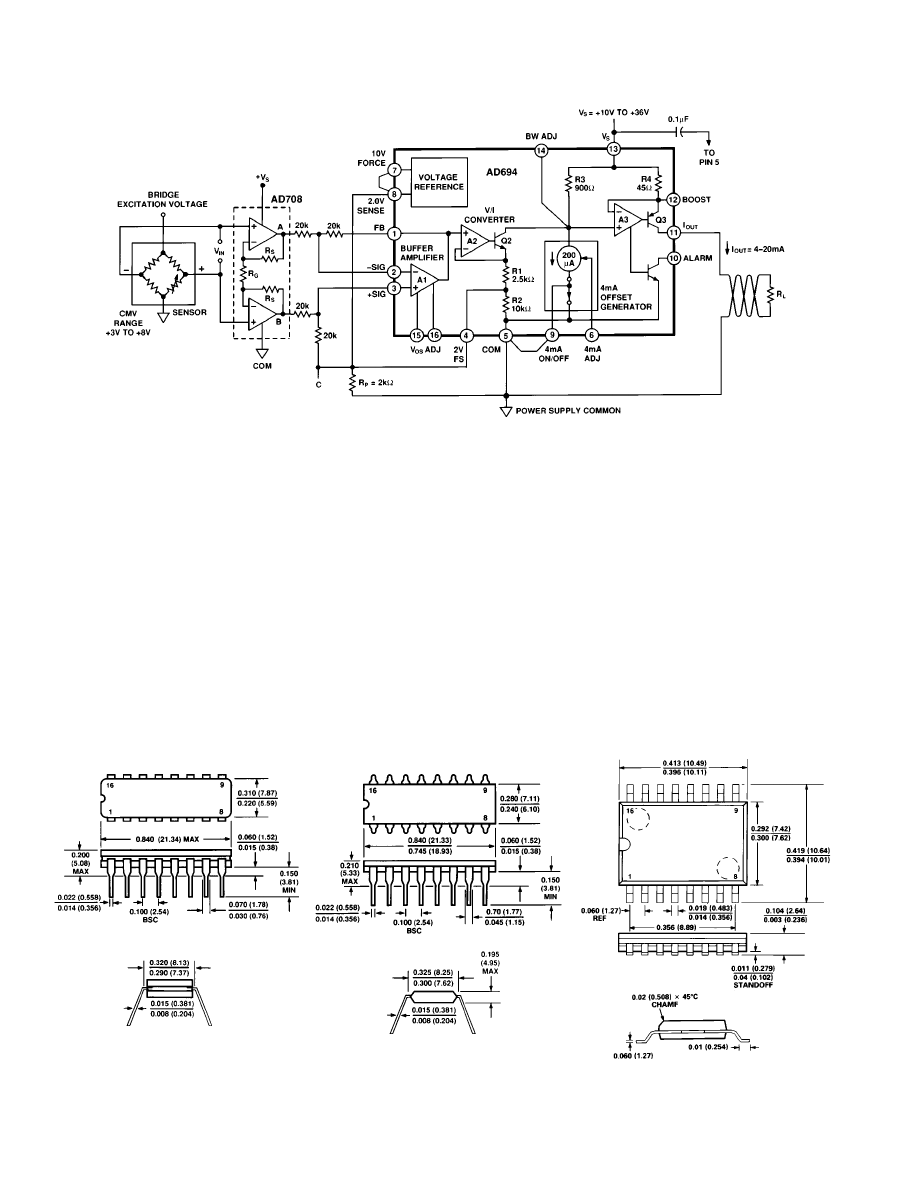
LOW COST SENSOR TRANSMITTER
Sensor bridges typically output differential signals in the 10 mV
to 100 mV full-scale range. With an AD694, a dual op amp, and
some resistors, an instrumentation amplifier front end can be
added which easily handles these types of low level signals.
The traditional 3 op amp instrumentation amplifier is built us-
ing an AD708, dual op amp for the front end, and the AD694’s
buffer amplifier is used for the subtractor circuit, as shown in
Figure 15. The AD694’s 2 V reference is used to provide a
“ground” of 2 V that insures proper operation of the in amp
over a wide common mode range. The reference pin of the
subtractor circuit is tied to the 2 V reference (point C). A 2 k
Ω
pull-down resistor insures that the voltage reference will be able
to sink any subtractor current. The 2 V FS (Pin 4) is attached to
the 2 V reference; this offsets the input range of the V/I con-
verter 2 volts positive, to match the “ground” of the in amp.
AD694
–12–
REV. A
C1403a–10–8/91
PRINTED IN U.S.A.
Figure 15. Low Cost Sensor Transmitter
The AD694 will now output a 4-20 mA output current for a 0
to 2 V differential swing across V
A
. The gain of the in amp front
end is adjusted so that the desired full-scale input signal at V
IN
results in a V
A
of 2 V. For example a sensor that has a 100 mV
full scale will require a gain of 20 in the front end. The gain is
determined according to the equation:
G = [2R
S
/Rg] + 1
The circuit shown, will convert a positive differential signal at
V
IN
to a 4-20 mA current. The circuit has common-mode range
of 3 V to 8 V. The low end of the common-mode range is limited
by the AD708’s ability to pull down on R
S
. A single supply am-
plifier could be used instead to extend the common-mode range
down to about 1.5 V.
As shown, the circuit handles positive differential signals, (V
IN
positive). To handle bipolar differential signals (V
IN
is positive
or negative), the reference pin of the in amp (point C) must be
offset positively from the 2 V reference. For example, discon-
nected point C from the 2 V reference and connecting it to a
3 V source would result in a V
A
of 1 V, (or half scale) for a zero
volt differential input from the sensor.
OUTLINE DIMENSIONS
Dimensions shown in inches and (mm).
16-Pin SOIC (R) Package
16-Lead Cerdip
(Q) Package
16-Lead Plastic DIP
(N) Package
Wyszukiwarka
Podobne podstrony:
ad694 3 id 51121 Nieznany (2)
Abolicja podatkowa id 50334 Nieznany (2)
4 LIDER MENEDZER id 37733 Nieznany (2)
katechezy MB id 233498 Nieznany
metro sciaga id 296943 Nieznany
perf id 354744 Nieznany
interbase id 92028 Nieznany
Mbaku id 289860 Nieznany
Probiotyki antybiotyki id 66316 Nieznany
miedziowanie cz 2 id 113259 Nieznany
LTC1729 id 273494 Nieznany
D11B7AOver0400 id 130434 Nieznany
analiza ryzyka bio id 61320 Nieznany
pedagogika ogolna id 353595 Nieznany
Misc3 id 302777 Nieznany
cw med 5 id 122239 Nieznany
więcej podobnych podstron