1
LTC1729 Series
■
Trickle Charge Preconditioning If Cell < 2.7V
■
Charging Enabled When 0
°
C < T < 50
°
C
■
Built-In Termination: 3-Hour Time-Out
■
C/10 Detection with Status Indicator
■
Automatic Charger Present Detection
■
Automatic Battery Present Detection
■
1- or 2-Cell, 4.1V/Cell or 4.2V/Cell Options
■
Precision Internal 0.2% Voltage Feedback Divider
■
Compatible with LT1505/LT1510/LT1511/
LT1512/LT1513/LT1769
■
Small Footprint/Low Profile
The LTC
®
1729 series is a family of smart termination
controllers for lithium-ion battery chargers. These ICs
provide trickle charge preconditioning, temperature charge
qualification, time or charge current termination, auto-
matic charger and battery detection and status output.
Combining the LTC1729 series part with the LT
®
1510
(1.5A), LT1769 (2A), LT1511 (3A) and LT1505 (> 4A)
step-down chargers is a simple operation. Connecting six
pins from the LTC1729 series part to the step-down
chargers completes the integration. The LTC1729 termi-
nation controllers are also compatible with step-down/
step-up (SEPIC) chargers, including the LT1512 (2A switch)
and LT1513 (3A switch).
The LTC1729 series is available in the 8-pin MSOP and SO
packages.
■
Cellular Phones
■
PDAs
■
Cradle Chargers
■
Camcorders
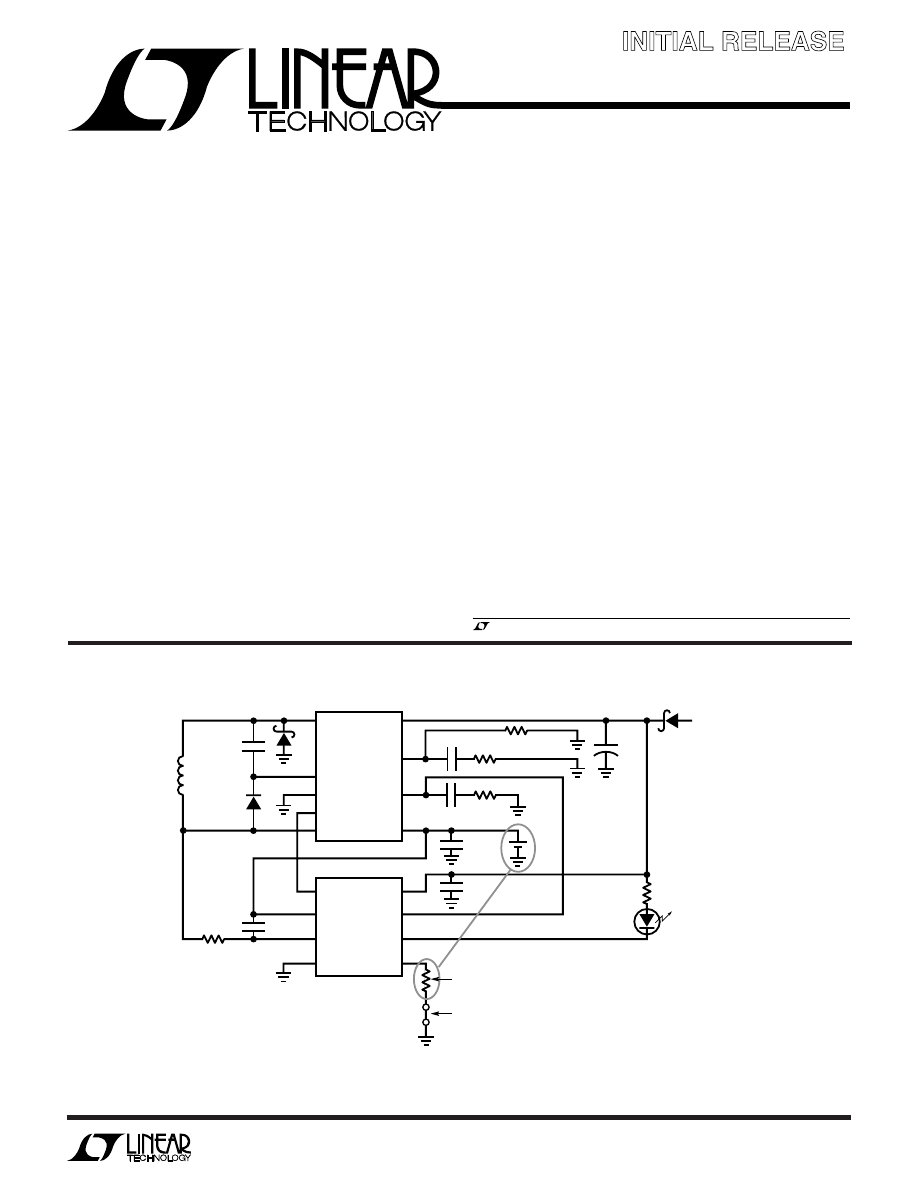
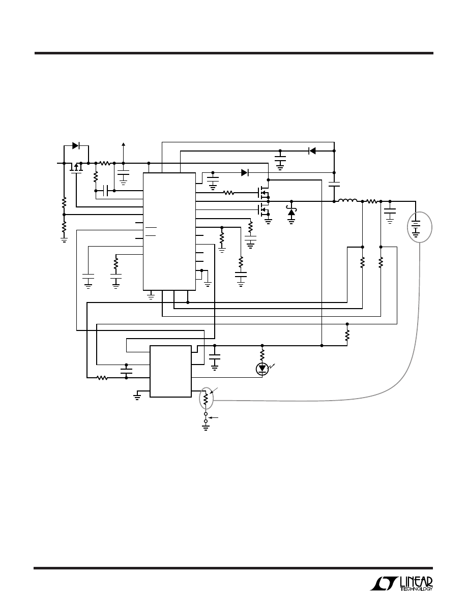
Figure 1. 500kHz Li-Ion Cell Phone Charger (0.8A)
Li-Ion Battery Charger
Termination Controllers
October 1999
FEATURES
DESCRIPTIO
N
U
APPLICATIO
N
S
U
TYPICAL APPLICATIO
N
U
, LTC and LT are registered trademarks of Linear Technology Corporation.
OVP
BAT
SENSE
GND
V
CC
V
C
STATUS
NTC
SW
SENSE
OVP
GND
BOOST
PROG
V
C
BAT
1
2
3
4
8
7
6
5
LTC1729-4.2
LT1510-5
1
µ
F
0.22
µ
F
L1**
10
µ
H
0.1
µ
F
1729 F01
OPTION: TIE RESISTOR TO STATUS FOR
CHARGE TERMINATION AT
LOW CHARGING CURRENT
* TOKIN OR MARCON SURFACE MOUNT
** COILTRONICS TP3-100, 10
µ
H, 2.2mm HEIGHT
(0.8A CHARGING CURRENT)
COILTRONICS TP1 SERIES, 10
µ
H, 1.8mm
HEIGHT (<0.5A CHARGING CURRENT)
*** PANASONIC EEFCD1B220
†
LUMEX SML-LX0805GW-TR
10k NTC THERMISTOR, NTHS1206N02 VISHAY/DALE
NOTE: EITHER A THERMISTOR OR 10k RESISTOR MUST BE PRESENT
0.1
µ
F
1
µ
F
1k
C
OUT
***
22
µ
F
4.2V
200
Ω
300
Ω
6.19k
+
+
C
IN
*
10
µ
F
MBRM120T3
INPUT POWER
8.2V TO 20V
D1
†
CHARGE STATUS
MBRM120T3
MMBD914L
V
CC
1.4k
Final Electrical Specifications
Information furnished by Linear Technology Corporation is believed to be accurate and reliable.
However, no responsibility is assumed for its use. Linear Technology Corporation makes no represen-
tation that the interconnection of its circuits as described herein will not infringe on existing patent rights.
2
LTC1729 Series
LTC1729CMS8-4.1
LTC1729CMS8-4.2
LTC1729CMS8-8.2
LTC1729CMS8-8.4
T
JMAX
= 150
°
C,
θ
JA
= 150
°
C/ W
ORDER PART
NUMBER
V
CC
......................................................................... 30V
SENSE, V
BAT
, NTC .................................... – 0.3V to 15V
V
C
............................................................. – 0.3V to 15V
OVP ............................................................ – 0.3V to 5V
(Note 1)
ABSOLUTE
M
AXI
M
U
M
RATINGS
W
W
W
U
PACKAGE/ORDER I
N
FOR
M
ATIO
N
W
U
U
ELECTRICAL CHARACTERISTICS
Consult factory for Industrial and Military grade parts.
The
●
denotes specifications which apply over the full operating temperature range, otherwise specifications are TA = 25
°
C, V
IN
= 8V.
1
2
3
4
OVP
BAT
SENSE
GND
8
7
6
5
V
CC
V
C
STATUS
NTC
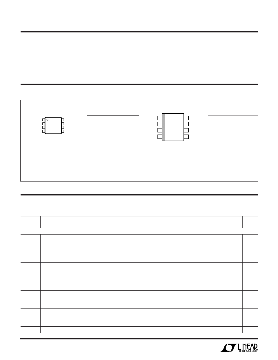
TOP VIEW
MS8 PACKAGE
8-LEAD PLASTIC MSOP
T
JMAX
= 150
°
C,
θ
JA
= 200
°
C/ W
MS8 PART MARKING
LTLY
LTJH
LTLZ
LTJG
TOP VIEW
OVP
BAT
SENSE
GND
V
CC
V
C
STATUS
NTC
S8 PACKAGE
8-LEAD PLASTIC SO
1
2
3
4
8
7
6
5
LTC1729CS8-4.1
LTC1729CS8-4.2
LTC1729CS8-8.2
LTC1729CS8-8.4
ORDER PART
NUMBER
S8 PART MARKING
STATUS .................................................... – 0.3V to 30V
Operating Temperature Range .................... 0
°
C to 70
°
C
Storage Temperature Range ................ – 65
°
C to 150
°
C
Lead Temperature (Soldering, 10 sec)................. 300
°
C
LTC1729-4.1/LTC1729-4.2
SYMBOL
PARAMETER
CONDITIONS
MIN
TYP
MAX
UNITS
DC CHARACTERISTICS
I
VIN
V
CC
Supply Current
V
IN
= 5V (Below UVLO)
●
1
5
12
µ
A
V
IN
= 8V, 200
µ
A Pull-Up on V
BAT
(4.5V) No Bat
●
1.0
1.4
2.0
mA
V
IN
= 8V, V
BAT
= 2.5V Trickle
10
17
21
mA
V
IN
= 8V, V
BAT
= 3.5V Charge
●
0.5
3.0
5.0
mA
V
LKOH
V
IN
Undervoltage Lockout High
●
5.5
6.5
7.5
V
V
LKOL
V
IN
Undervoltage Lockout Low
●
5.0
6.0
7.0
V
I
VBAT
V
BAT
Current
V
IN
= 5V (Below UVLO), V
BAT
= 4.2V
●
– 1
– 0.1
1
µ
A
V
IN
= 8V, V
BAT
= 4.25V No Bat
●
40
73
120
µ
A
V
IN
= 8V, V
BAT
= 2.5V Trickle
– 19
– 16
– 9.5
mA
V
IN
= 8V, V
BAT
= 3.5V Charge
●
– 2.7
– 1.3
– 0.5
mA
V
CLAMP
V
BAT
Clamp
No Bat (External 200
µ
A Pull-Up on V
BAT
)
●
4.25
4.5
4.75
V
V
MAX
High V
BAT
Threshold
High Going Threshold
●
4.25
4.51
4.75
V
Low Going Threshold
●
4.25
4.50
4.75
V
V
MIN
Low V
BAT
Threshold
High Going Threshold
●
2.55
2.7
2.85
V
Low Going Threshold
●
2.45
2.6
2.75
V
I
SENSE
SENSE Pin Current
Charge State, V
SENSE
= 3V
●
85
100
115
µ
A
V
C10
SENSE Pin C/10 Offset
Charge State, V
C10
= (V
BAT
– V
SENSE
)
●
±
1
±
2.5
mV
172941
172942
172982
172984
3
LTC1729 Series
The
●
denotes specifications which apply over the full operating temperature range, otherwise specifications are TA = 25
°
C, V
IN
= 8V.
LTC1729-4.1/LTC1729-4.2
SYMBOL
PARAMETER
CONDITIONS
MIN
TYP
MAX
UNITS
I
NTC
NTC Pin Current
V
NTC
= 1V
●
90
100
110
µ
A
V
NTC-RESET
Thermistor Pin Reset Threshold
●
0.160
0.206
0.240
V
V
NTC-HOT
Thermistor Pin Hot Hold Threshold
High Going Threshold
●
0.460
0.486
0.510
V
Low Going Threshold
●
0.380
0.405
0.430
V
V
NTC-COLD
Thermistor Pin Cold Hold Threshold
High Going Threshold
●
2.70
2.79
2.90
V
Low Going Threshold
●
2.10
2.23
2.35
V
V
OVP
OVP Pin Voltage
V
BAT
= 4.1V or V
BAT
= 4.2V
●
2.455
2.465
2.475
V
2.460
2.465
2.470
V
V
OL-ST
Output Low Voltage-STATUS Pin
I
O
= 3mA
●
0.5
0.9
1.2
V
V
OL-VC
Output Low Voltage-V
C
Pin
I
O
= 1mA
●
0.35
0.6
0.75
V
I
SOFT
Status Soft Pull-Down Current
V
STATUS
= 4.5V
●
40
50
65
µ
A
ELECTRICAL CHARACTERISTICS
The
●
denotes specifications which apply over the full operating temperature range, otherwise specifications are TA = 25
°
C,
V
IN
= 12V
LTC1729-8.2/LTC1729-8.4
SYMBOL
PARAMETER
CONDITIONS
MIN
TYP
MAX
UNITS
DC CHARACTERISTICS
I
VIN
V
CC
Supply Current
V
IN
= 9V (Below UVLO)
●
1
6
12
µ
A
V
IN
= 12V, 200
µ
A Pull-Up on V
BAT
(9V) No Bat
●
1.0
1.4
2.0
mA
V
IN
= 12V, V
BAT
= 5V Trickle
10
17
21
mA
V
IN
= 12V, V
BAT
= 7V Charge
●
0.5
3.0
5.0
mA
V
LKOH
V
IN
Undervoltage Lockout High
●
9.5
10.4
11.4
V
V
LKOL
V
IN
Undervoltage Lockout Low
●
8.5
9.6
10.5
V
I
VBAT
V
BAT
Current
V
IN
= 9V (Below UVLO), V
BAT
= 8.4V
●
– 1
– 0.1
1
µ
A
V
IN
= 12V, V
BAT
= 8.5V No Bat
●
60
95
140
µ
A
V
IN
= 12V, V
BAT
= 5V Trickle
– 19
– 16
– 9.5
mA
V
IN
= 12V, V
BAT
= 7V Charge
●
– 2.7
– 1.3
– 0.5
mA
V
CLAMP
V
BAT
Clamp
No Bat (External 200
µ
A Pull-Up on V
BAT
)
●
8.5
9
9.5
V
V
MAX
High V
BAT
Threshold
High Going Threshold
●
8.5
9.013
9.5
V
Low Going Threshold
●
8.5
9
9.5
V
V
MIN
Low V
BAT
Threshold
High Going Threshold
●
5.1
5.4
5.7
V
Low Going Threshold
●
4.9
5.2
5.5
V
I
SENSE
SENSE Pin Current
Charge State, V
SENSE
= 7V
●
85
100
115
µ
A
V
C10
SENSE Pin C/10 Offset
Charge State, V
C10
= (V
BAT
– V
SENSE
)
●
±
1
±
2.5
mV
I
NTC
NTC Pin Current
V
NTC
= 1V
●
90
100
110
µ
A
V
NTC-RESET
Thermistor Pin Reset Threshold
●
0.160
0.206
0.240
V
V
NTC-HOT
Thermistor Pin Hot Hold Threshold
High Going Threshold
●
0.460
0.486
0.510
V
Low Going Threshold
●
0.380
0.405
0.430
V
V
NTC-COLD
Thermistor Pin Cold Hold Threshold
High Going Threshold
●
2.70
2.79
2.90
V
Low Going Threshold
●
2.10
2.23
2.35
V
V
OVP
OVP Pin Voltage
V
BAT
= 8.2V or V
BAT
= 8.4V
●
2.455
2.465
2.475
V
2.460
2.465
2.470
V
V
OL-ST
Output Low Voltage-STATUS Pin
I
O
= 3mA
●
0.5
0.9
1.2
V
V
OL-VC
Output Low Voltage-V
C
Pin
I
O
= 1mA
●
0.35
0.6
0.75
V
I
SOFT
Status Soft Pull-Down Current
V
STATUS
= 4.5V
●
40
50
65
µ
A
4
LTC1729 Series
ELECTRICAL CHARACTERISTICS
The
●
denotes specifications which apply over the full operating temperature range, otherwise specifications are TA = 25
°
C. (Note 2)
SYMBOL
PARAMETER
CONDITIONS
MIN
TYP
MAX
UNITS
AC CHARACTERISTICS
TIMER1
Timer for Trickle-Charge Preconditioning
●
0.869
1
1.305
Hr
TIMER2
Timer for Charging
●
2.61
3
3.55
Hr
TIMER3
Timer for V
MAX
Filter
●
0.764
0.859
1.043
sec
TIMER4
Timer for V
C/10
Filter
●
3.055
3.5
4.17
sec
T
OSC
Oscillator Period
●
6.66
7.63
9.09
µ
s
OVP (Pin 1): Output from an Internal Precision Resistor
Divider Used as a Voltage Feedback Monitor for Constant-
Voltage Mode Charging.
BAT (Pin 2): Input to Battery Monitor Circuits and OVP
Resistor Divider. The battery monitor circuits activate
trickle charge preconditioning, battery present detection
and C/10 current detection. This pin is in a high impedance
state when V
CC
is below the undervoltage lockout thresh-
old. During trickle charge preconditioning and charging
the BAT pin sources 16mA and 1.3mA respectively. The
current sources are clamped from driving the BAT pin
above 4.5V/cell with an internal pull-down transistor.
In the No Bat, Done and Pause states or the Hold and Reset
modes, the current sources are turned off, leaving only the
55k OVP divider as a load on the BAT pin. Most chargers
have a 200
µ
A current source that will compensate for this
50
µ
A to 80
µ
A load.
SENSE (Pin 3): Input to C/10 Current Detection Circuit.
This pin sinks 100
µ
A during the Charge state which is used
to program the C/10 current threshold.
GND (Pin 4): Ground.
NTC (Pin 5): Input to the NTC Thermistor Monitoring
Circuits. When the voltage on this pin is above 2.79V
(cold) or below 0.405V (hot), the state machine is locked
in the present state and the timer is stopped. This is called
the Hold mode. While in the Hold mode, the charger is
turned off via the V
C
pin and the current sources on BAT
and SENSE pins are turned off. The STATUS pin is not
affected.
PI
N
FU
N
CTIO
N
S
U
U
U
Note 1: Absolute Maximum Ratings are those values beyond which the life
of a device may be impaired.
If the NTC pin is below 0.2V, the state machine is forced
in the reset mode with all the timers cleared to zero. The
current sources on the BAT pin and SENSE pin are
disabled leaving the 55k OVP divider. The STATUS pin is
pulled low in the Reset mode.
There is a 100
µ
A current source on the NTC pin to bias the
NTC thermistor. This current source is active while the V
CC
is greater than the undervoltage lockout threshold.
STATUS (Pin 6): Open-Drain Output for C/10 Charge
Termination Detection Circuit. When in the Charge state,
this pin is pulled low. Once the charge current drops below
the C/10 current threshold for three seconds, the pull-
down transistor is disabled, and a 50
µ
A pull-down current
sink remains activated until the 1- or 3-hour time-out or
the battery or wall adapter is removed.
V
C
(Pin 7): Open-Drain Output for turning off the charger.
When this pin is open circuit, the charger is active.
Normally this pin allows the charger to be active for three
hours.
V
CC
(Pin 8): Input Supply. For 4.1V or 4.2V single cell
operation, V
CC
should be between 8V and 28V with the IC
turning off when V
CC
drops below 6V. For 2-cell applica-
tions, the undervoltage lockout is 10.4V with a minimum
V
CC
of 12V. Removing the wall adapter will trigger an
undervoltage lockout and put the part in a high impedance
condition. When the supply is connected, the part is
initialized in the Reset mode with the state machine forced
in the Charge state with all the timers set to zero.
Note 2: V
IN
= 8V for LTC1729-4.1/LTC1729-4.2; V
IN
= 12V for
LTC1729-8.2/LTC1729-8.4
5
LTC1729 Series
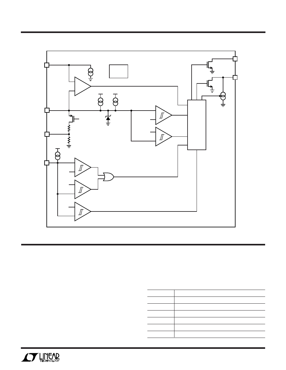
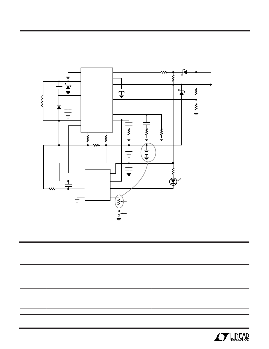
BLOCK DIAGRA
W
BAT
3
2
OVP
1
NTC 5
SENSE
STATUS
100
µ
A
1729 F02
6
V
C
7
–
+
COMP1
–
+
COMP4
UVLO
2.465V
2.79V
100
µ
A
1.3mA
16mA
4.5V/CELL
CLAMP
–
+
COMP2
4.5V/CELL
–
+
COMP3
V
MIN
V
MAX
C/10
HOLD
RESET
2.7V/CELL
–
+
COMP5
0.405V
–
+
COMP6
0.2V
LOGIC
AND
TIMER
UVLO
M1
M2
M3
50
µ
A
Figure 2. Block Diagram
APPLICATIO
N
S I
N
FOR
M
ATIO
N
W
U
U
U
Overview
The LTC1729 is a charge termination controller for the
LT1505/LT1510/LT1511/LT1512/LT1513/LT1769 con-
stant-voltage/constant-current battery charger family.
Table 1 details these chargers. The primary function of this
IC is to stop the charger after three hours of constant-
voltage/constant-current charging. The secondary func-
tion of this controller includes an indication when the
charge current (during constant-voltage mode) drops
below a user-selected threshold. A 500kHz Li-Ion cell
phone charger is shown in Figure 1. The LTC1729 only
needs six external components when combined with the
standard LT1510 application. The LTC1729 provides a
complete and tiny solution for cellular phones and other
portable applications.
Table 1. Battery Chargers
LT1505
4A Step-Down Charger with Input Current Limit
LT1510
1.5A Step-Down Charger
LT1510-5
1.5A 500kHz Step-Down Charger
LT1511
3A Step-Down Charger with Input Current Limit
LT1512
2A Switch SEPIC Charger
LT1513
3A Switch SEPIC Charger
LT1769
2A Step-Down Charger with Input Current Limit
6
LTC1729 Series
APPLICATIO
N
S I
N
FOR
M
ATIO
N
W
U
U
U
Block Diagram
Figure 2 shows the block diagram of the LTC1729. The IC
consists of six comparators, a resistive divider, a UVLO
block and a logic and timer block.
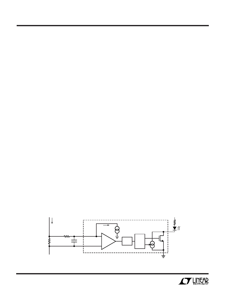
The comparator COMP1 is used to indicate C/10 charge
current threshold. (“C” is a term used to indicate the
Ampere-hour capacity of a cell.) Figure 3 details the C/10
detection circuit. The resistor and capacitor on the SENSE
pin filter the signal from the 0.2
Ω
current sense resistor
R1. The 100
µ
A current sink on the SENSE pin develops
20mV across the 200
Ω
resistor R2. This sets a 20mV
offset on COMP1 that sense resistor R1 must equal before
C/10 current is indicated. The C/10 is not recognized by the
logic until it passes through a 3-second digital filter.
For cases where there are multiple batteries to be charged,
the LTC1729 detects when a battery is removed and resets
the timers for the next charge cycle. The battery present
detection is the primary function of comparator COMP2.
When the battery is disconnected from the LTC1729, the
voltage at the BAT pin will begin ramping upward. This is
due to a current source inside the charger or an external
pull-up resistor. Once the voltage on the BAT pin exceeds
the 4.5V/cell limit, COMP2 signals a V
MAX
= true to the
logic and turns on a transistor that clamps the voltage.
There is the possibility of an overvoltage transient at the
charging terminals. This occurs if the battery protection
circuit, which is often included in the battery pack, opens
the connection to the battery during high current charging
(constant-current mode). This is a result of energy storage
in the inductor. COMP2 senses the overvoltage and clamps
100
µ
A
50
µ
A
1729 F03
–
+
COMP1
STATUS
V
CC
CHARGE
LED
LTC1729
SENSE
BAT
+
+
–
–
R2
200
Ω
20mV
I
BIAS
20mV
R1
0.2
Ω
CHARGING
CURRENT
C1
1
µ
F
3-SEC
FILTER
LOGIC
AND
TIMERS
Figure 3. C/10 Detection Circuit
the V
C
pin, reducing the duty cycle of the charger. If the
battery protection circuit quickly returns battery connec-
tion to the charger (in less than one second), then the
LTC1729 continues charging without resetting the timers.
For a battery that has been over-discharged, the LTC1729
provides a 16mA start-up current. This preconditioning
trickle charge begins when the battery voltage drops
below 2.7V/cell. Comparator COMP3 is used to determine
when this condition exists. The battery operating range is
summarized in Figure 4.
With a 10k negative TC thermistor connected to the NTC
pin, the LTC1729 will disable charging if the temperature
is not in the 0
°
C to 50
°
C range. A thermistor must be
present at this pin, or if the temperature qualification
feature is not used, a 10k resistor must be used in its place.
This pin should not be left open. The NTC thermistor
monitoring circuits consist of COMP4, COMP5 and COMP6.
The NTC pin voltage range is shown in Figure 5.
Comparators COMP4 and COMP5 signal the logic when
the temperature is below 0
°
C or above 50
°
C. The 100
µ
A
bias current through the 10k
Ω
thermistor will generate
2.79V at 0
°
C and 0.405V at 50
°
C. The voltage hysteresis
on COMP4 and COMP5 is designed to give 10
°
C of
temperature hysteresis. If the voltage on the NTC pin
drops below 0.2V, the comparator COMP6 generates a
reset to the logic and timer block.
To provide accurate charge voltages, the internal resistor
divider is trimmed to provide a precise
±
0.2% voltage of
2.465V at the OVP pin for the four battery voltage options
of 4.1V, 4.2V, 8.2V and 8.4V.
7
LTC1729 Series
APPLICATIO
N
S I
N
FOR
M
ATIO
N
W
U
U
U
V
MAX
= 1V
V
MIN
= 0V
4.5V/CELL
BATTERY CLAMP
PULL-DOWN
ON
V
MAX
= 0V
V
MIN
= 0V
2.7V/CELL
NORMAL CHARGE
BA
TTER
Y VOL
TAGE
V
MAX
= 0V
V
MIN
= 1V
TRICKLE CHARGE
PRECONDITIONING
1729 F04
HOLD MODE
2.79V
THERMISTOR VOL
TAGE
HOLD MODE
0.2V
RESET MODE
NORMAL CHARGE
0.405V
1729 F05
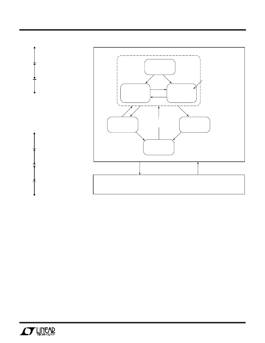
The logic and timer block consists of a state machine,
oscillator and counter. The state machine will be dis-
cussed in detail in the next section. The oscillator is
internally trimmed to 131kHz. The counter is composed of
a chain of 25 flip-flops that includes self-test circuitry.
State Machine
The state machine is responsible for the following items:
1. When to start and stop the charger. The internal timer
must be initialized every time a new battery is installed
or when the input supply is applied.
2. When a battery is installed, the state machine must
determine if it is a new battery or if the previous battery
has been reinstalled.
Figure 4. BAT Voltage Operating Range
Figure 5. NTC Voltage Operating Range
When the input supply is removed in step-down charger
designs, the V
CC
pin does not drop to 0V, but is held to a
diode drop below the battery voltage. This is due to the
internal parasitic diode from the SW pin to the V
CC
pin that
is present in the LT1510, LT1511, LT1769, and the body
diode of the top MOSFET in the LT1505 charger. Removing
the input supply will result in the V
CC
pin dropping below
the UVLO threshold, thus shutting down the LTC1729 and
minimizing battery drain. Once the input supply is con-
nected, the LTC1729 resets the timers and begins another
charge cycle. There is a disconnect transistor that will
remove the OVP resistor divider from the battery when the
V
CC
voltage drops below the UVLO threshold.
RESET MODE
I
BAT
= 0
STATUS = PULL-DOWN
V
C
= PULL-DOWN
PAUSE
I
BAT
= 0
STATUS = PULL-DOWN
V
C
= PULL-DOWN
DONE
I
BAT
= 0
STATUS = OPEN
V
C
= PULL-DOWN
NO BAT
I
BAT
= 0
STATUS = OPEN
V
C
= PULL-DOWN
HOLD MODE
I
BAT
= 0
STATUS = PREVIOUS STATUS
V
C
= PULL-DOWN
PRECONDITION
I
BAT
= 16mA
STATUS = PULL-DOWN
V
C
= PULL-DOWN
t
MAX
= 1HR
V
BAT
< V
MIN
V
BAT
> V
MIN
V
BAT
> V
MAX
TIME > t
MAX
1729 F06
NOTE: FOR STATUS
PULL-DOWN = HARD:
FOR CURRENT > C/10
PULL-DOWN = 50
µ
A:
FOR CURRENT < C/10 FOR 3SEC
V
BAT
< V
MAX
FOR MORE THAN 1SEC
V
BAT
< V
MAX
FOR MORE THAN 1SEC
V
BAT
> V
MAX
FOR MORE THAN 1SEC
V
BAT
> V
MAX
FOR MORE THAN 1SEC
V
NTC
> 2.79V OR
V
NTC
< 0.405V
V
NTC
< 2.79V AND
V
NTC
> 0.405V
V
BAT
> V
MIN
V
BAT
< V
MIN
CHARGER “ON”
I
BAT
= 1.3mA
STATUS = PULL-DOWN
V
C
= OPEN
t
MAX
= 3HR
CHARGE
Figure 6. State Diagram

8
LTC1729 Series
3. When a heavily discharged battery is installed, trickle
charge conditioning must take place before the full
charge current.
The state machine diagram is shown in Figure 6. Note that
the Charge state includes the Precondition state, the
charger “ON” state and the Reset mode.
Reset and Hold are the two modes that will cause the
charger to stop charging (V
C
pin pulled low) and ignore the
state machine. The Reset mode clears all the timers and
forces the state machine to begin in the Charge state
(STATUS pin pulled low). This mode is only activated
momentarily at power-up or when the NTC pin is below the
Reset threshold. The other interrupt condition is called the
Hold mode. When the voltage on the NTC pin is above
2.79V (cold) or below 0.405V (hot), the state machine is
locked in the present state until the NTC pin voltage returns
to the proper range. While in the Hold mode, the charging
is disabled and the timers are frozen.
The charger is enabled only during the charger “ON” state.
There are three ways that the state machine can exit the
charger “ON” state. The first is for a 3-hour time-out which
is denoted as the time > t
MAX
transition to the Done state.
Second, if the battery is removed from the charger, the
V
MAX
signal is activated as mentioned in the Block Dia-
gram section. This causes the state machine to make the
V
BAT
> V
MAX
transition to the Pause state. The third way to
exit the charger “ON” state is with a V
BAT
< V
MIN
transition
to the Precondition state. The battery will need to drop
below 2.6V/cell to be less than V
MIN
. This is not a likely
scenario.
Once in the Pause state, there are two ways to proceed.
The first is to go to the No Bat state. This requires that the
V
BAT
remain greater than V
MAX
for more than one
second. From these conditions, the LTC1729 interprets
that a battery has been removed. If the voltage on the BAT
pin stays less than V
MAX
for more than one second, then
the state machine returns to the Charge state (Precondi-
tion and charger “ON”). This is interpreted as a momentary
open caused by the battery pack protection circuitry or
loose contact.
The Done state can only proceed to the No Bat state. From
outside the LTC1729 this transition is undetectable. The
APPLICATIO
N
S I
N
FOR
M
ATIO
N
W
U
U
U
requirement for this transition is for the BAT pin voltage to
exceed V
MAX
for more than one second. The IC now
assumes that the battery has been removed.
From the No Bat state, there is only one possible transition.
The No Bat state can move to the Charge state if the voltage
on the BAT pin remains less than V
MAX
for one second. The
LTC1729 will now work on the assumption that a new
battery has been installed.
Although the Precondition and Charger “ON” both reside
in the Charge state, there are differences between these
states. The main purpose of the Precondition state is to
slowly bring a heavily discharged battery up to a minimum
level before full charge current begins. The Precondition
state uses a 16mA current source to trickle charge the
battery with a 1-hour time-out transition to the Done state.
The Charger “ON” state enables the external charger and
the time-out is increased to three hours. For the entire
time in the Precondition state, the STATUS pin uses a hard
pull-down. In the Charger “ON” state the STATUS pin uses
two types of pull-down: hard pull-down and soft 50
µ
A
pull-down.
The STATUS pin is designed to provide an indication that
the battery is charging. Once the current drops below the
C/10 threshold, the battery is close to being fully charged.
The LTC1729 turns off the hard pull-down once the
C/10 comparator is active for more than three seconds.
The 50
µ
A soft pull down remains in effect until the 3-hour
time-out is completed or the input power is removed.
Terminate at C/10 Current
Charging can also be terminated using C/10 detection
rather than the 3-hour time-out. By connecting the low
side of the NTC thermistor to the STATUS pin instead of
ground, the NTC pin will float to 5V as soon as the Status
pull-down is open. This will force the state machine into
the Hold mode. The V
C
pin is pulled low which turns off the
charger. This circuit is shown in Figure 7.
In order to restart the charging process for a new battery,
the NTC pin will need to be momentarily brought below
0.2V or the V
CC
pin brought below the UVLO threshold.
The automatic battery detection features are disabled
during the Hold mode.
9
LTC1729 Series
APPLICATIO
N
S I
N
FOR
M
ATIO
N
W
U
U
U
OVP
BAT
SENSE
GND
OVP
BAT
SENSE
V
CC
V
C
STATUS
NTC
V
C
V
CC
1
2
3
4
8
7
6
5
LTC1729-4.2
1
µ
F
0.1
µ
F
1729 F07
10k NTC THERMISTOR
NTHS1206N02 VISHAY/DALE
200
Ω
Figure 7. Terminate Charging at C/10
100
µ
A
1729 F08
–
+
COMP1
LTC1729
SENSE
I
BIAS
BAT
+
–
SENSE
RESISTOR
CHARGE
CURRENT
Figure 8. Modify C/10 Indication to Create Charging Indicator
TYPICAL APPLICATIO
N
S
U
SEPIC Charger with 0.5A Output Current
OVP
BAT
SENSE
GND
V
CC
V
C
STATUS
NTC
S/S
V
SW
GND
V
C
V
FB
I
FB
LTC1729-4.2
BOOST
CAP
+
GND
CAP
–
V
+
OSC
LV
V
OUT
LTC1044
LT1512
C4
0.22
µ
F
C1
22
µ
F
R3
0.2
Ω
R1
29.4k
D2
1/2 BAT85S
D3
1/2 BAT85S
FOR 3.5V TO 14V USE LTC1144
R2
12.4k
L1A**
C6
1
µ
F
1729 F11
OPTION: TIE R8 TO STATUS FOR
CHARGE TERMINATION AT
LOW CHARGING CURRENT
* TOKIN CERAMIC 1E225ZY5U-C203-F
** L1A, L1B ARE TWO 33
µ
H WINDINGS ON A
SINGLE INDUCTOR; COILTRONICS CTX33-3
†
LUMEX SML-LX0805GW-TR SIZE R9 FOR
20mA TYPICAL
R8
10k NTC THERMISTOR, NTHS1206N02 VISHAY/DALE
NOTE: EITHER A THERMISTOR OR 10k RESISTOR MUST BE PRESENT
R9
1k
R5
1k
C2*
2.2
µ
F
R7
100
Ω
R
PULLUP
10k
R4, 24
Ω
R6
0.2
Ω
L1B**
+
C3
22
µ
F
C7
10
µ
F
C8
10
µ
F
C5
0.1
µ
F
D1
MBRS130LT3
INPUT POWER
4V TO 9V
D4
†
V
IN
4.2V
+
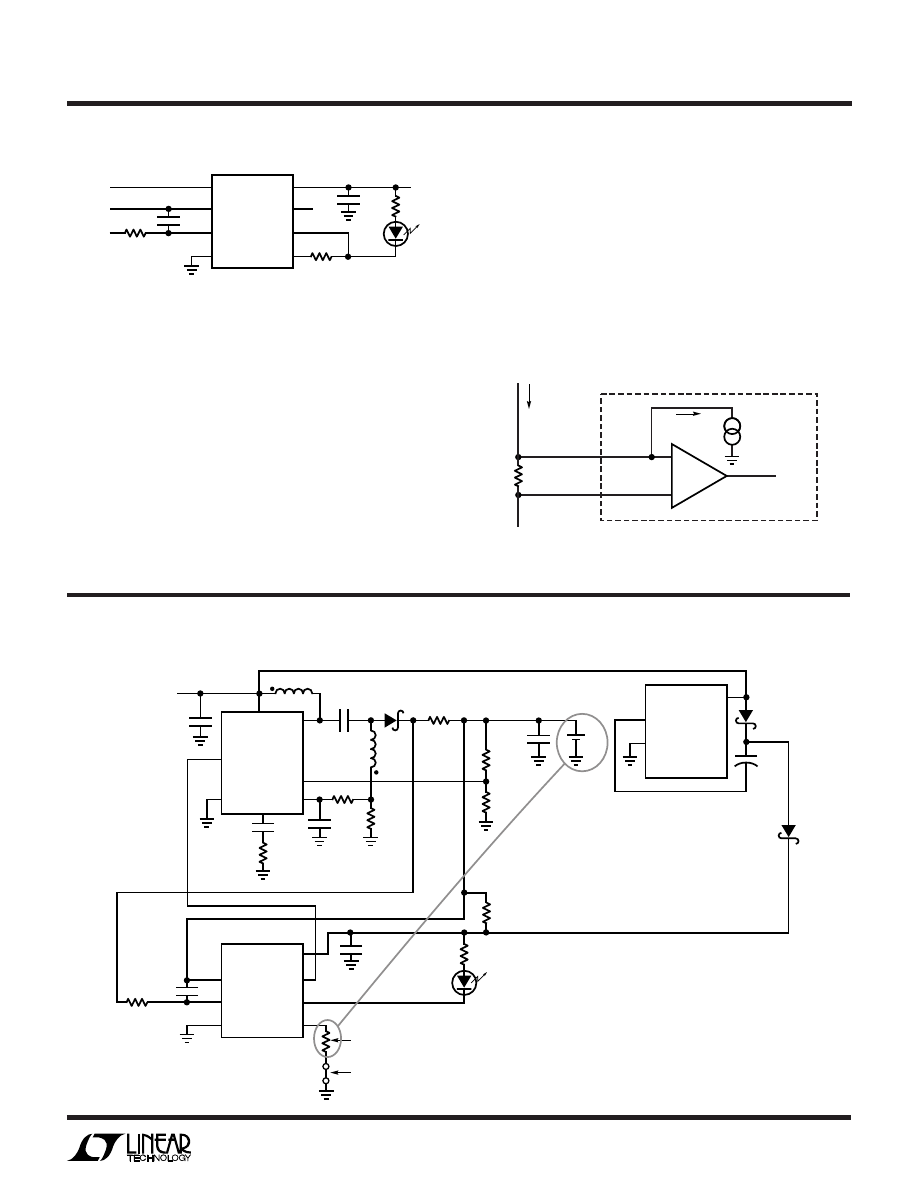
Using Status as a Charging Indicator
In many applications circuits shown in this data sheet, the
STATUS pin is used to indicate when C/10 has occurred
(charge current has dropped to 10% of the full charge
current). This C/10 number is not fixed, but is set by an
external resistor connected to the LTC1729 SENSE pin. A
100
µ
A bias current through this resistor develops a volt-
age which is compared with the voltage across the charge
current sense resistor. When these voltages are equal, the
open-drain STATUS pin turns off. Connecting an LED to
the STATUS pin will give a visual indication during the
precondition trickle charge and the portion of the main
charge before C/10 has occurred.
By reducing the LTC1729 SENSE pin resistor to 0
Ω
, the
STATUS pin function can be changed to a
charging indica-
tor (Figure 8). The LED on the STATUS pin will always go
off after the 3-hour charge cycle is completed, regardless
of the C/10 circuitry.
10
LTC1729 Series
TYPICAL APPLICATIO
N
S
U
4A, 2-Cell Lithium-Ion Battery Charger
CLN
CLP
INFET
UV
SYNC
SHDN
FLAG
CAP
COMP1
GBIAS
TGATE
SW
BGATE
V
C
PROG
3 CELL
V
FB
4.2V
4.1V
AGND
PGND
TO
SYSTEM
POWER
BAT2 BAT SENSE SPIN
R
PROG
4.93k
1%
C
PROG
1
µ
F
BOOST BOOSTC
OVP
BAT
SENSE
GND
V
CC
V
C
STATUS
NTC
LTC1729-8.4
LT1505
C
IN
*
47
µ
F
35V
OPTION: TIE RESISTOR TO STATUS FOR
CHARGE TERMINATION AT
LOW CHARGING CURRENT
* SANYO OS-CON
** SUMIDA CDRH127-150
*** AVX TPSD226L025R0200
†
LUMEX SML-LX0805GW-TR
R
S1
0.025
Ω
R
S2
200
Ω
1%
R
S4
0.025
Ω
M3
Si4435
DBODY
V
IN
(FROM
ADAPTER)
R7
500
Ω
R5
3k
R1
1k
R4
3k
C5
0.33
µ
F
R6
5.1k
R
S3
200
Ω
1%
C1
1
µ
F
8.4V
+
D5
†
V
CC
C
OUT
***
22
µ
F
×
2
C9
0.1
µ
F
C8
0.1
µ
F
C7
0.68
µ
F
C3
2.2
µ
F
C4
0.1
µ
F
M1
Si4412
M2
Si4412
D2
MMSD4148
D3
MMSD4148
L1**
15
µ
H
D4
MBRS140
5
Ω
C2
0.68
µ
F
R3
300
Ω
C6
0.1
µ
F
R8
100
Ω
R9
1.4k
R
PULL-UP
10k
1729 F09
10k NTC THERMISTOR, NTHS1206N02 VISHAY/DALE
NOTE: EITHER A THERMISTOR OR 10k RESISTOR MUST BE PRESENT
11
LTC1729 Series
MS8 Package
8-Lead Plastic MSOP
(LTC DWG # 05-08-1660)
Dimensions in inches (millimeters) unless otherwise noted.
PACKAGE DESCRIPTIO
N
U
S8 Package
8-Lead Plastic Small Outline (Narrow 0.150)
(LTC DWG # 05-08-1610)
MSOP (MS8) 1098
* DIMENSION DOES NOT INCLUDE MOLD FLASH, PROTRUSIONS OR GATE BURRS. MOLD FLASH,
PROTRUSIONS OR GATE BURRS SHALL NOT EXCEED 0.006" (0.152mm) PER SIDE
** DIMENSION DOES NOT INCLUDE INTERLEAD FLASH OR PROTRUSIONS.
INTERLEAD FLASH OR PROTRUSIONS SHALL NOT EXCEED 0.006" (0.152mm) PER SIDE
0.021
±
0.006
(0.53
±
0.015)
0
°
– 6
°
TYP
SEATING
PLANE
0.007
(0.18)
0.040
±
0.006
(1.02
±
0.15)
0.012
(0.30)
REF
0.006
±
0.004
(0.15
±
0.102)
0.034
±
0.004
(0.86
±
0.102)
0.0256
(0.65)
BSC
1
2
3
4
0.193
±
0.006
(4.90
±
0.15)
8
7 6
5
0.118
±
0.004*
(3.00
±
0.102)
0.118
±
0.004**
(3.00
±
0.102)
0.016 – 0.050
(0.406 – 1.270)
0.010 – 0.020
(0.254 – 0.508)
×
45
°
0
°
– 8
°
TYP
0.008 – 0.010
(0.203 – 0.254)
SO8 1298
0.053 – 0.069
(1.346 – 1.752)
0.014 – 0.019
(0.355 – 0.483)
TYP
0.004 – 0.010
(0.101 – 0.254)
0.050
(1.270)
BSC
1
2
3
4
0.150 – 0.157**
(3.810 – 3.988)
8
7
6
5
0.189 – 0.197*
(4.801 – 5.004)
0.228 – 0.244
(5.791 – 6.197)
DIMENSION DOES NOT INCLUDE MOLD FLASH. MOLD FLASH
SHALL NOT EXCEED 0.006" (0.152mm) PER SIDE
DIMENSION DOES NOT INCLUDE INTERLEAD FLASH. INTERLEAD
FLASH SHALL NOT EXCEED 0.010" (0.254mm) PER SIDE
*
**
12
LTC1729 Series
1729i LT/TP 1099 4K • PRINTED IN USA
LINEAR TECHNOLOGY CORPORATION 1999
Linear Technology Corporation
1630 McCarthy Blvd., Milpitas, CA 95035-7417
(408) 432-1900
●
FAX: (408) 434-0507
●
www.linear-tech.com
RELATED PARTS
PART NUMBER
DESCRIPTION
COMMENTS
LT1505
High Efficiency Constant-Voltage/Constant-Current Battery Charger
Uses External Synchronous N-Channel FETs
LT1510
Constant-Voltage/Constant-Current Battery charger
Up to 1.5A Charge Current for Lithium-Ion, NiCd and
NiMH Batteries, Internal R
SENSE
LT1511
3A Constant-Voltage/Constant-Current Battery Charger
Charges Lithium, NiCd and NiMH Batteries
LT1512
SEPIC Battery Charger
V
IN
Can Be Higher or Lower Than Battery Voltage, 2A Switch
LT1513
SEPIC Battery Charger
V
IN
Can Be Higher or Lower Than Battery Voltage, 3A Switch
LTC1759
SMBus-Controlled Smart Battery Charger
LT1505 Charger Functionality with SMBus Control
LT1769
2A Constant-Voltage/Constant-Current Battery Charger
In 28-Pin SSOP Package
TYPICAL APPLICATIO
N
U
3A (LT1511) Or 2A (LT1769), 2-Cell Lithium-Ion Battery Charger
TO MAIN
SYSTEM
POWER
BAT
SENSE
OVP
BAT
SENSE
GND
V
CC
V
C
STATUS
NTC
LTC1729-8.4
LT1511 OR LT1769
OPTION: TIE RESISTOR TO STATUS FOR
CHARGE TERMINATION AT
LOW CHARGING CURRENT
* TOKIN C55Y5U1E156Z
** SUMIDA CDRH125-220MC
*** AVX TPSD226K025R0200
†
LUMEX SML-LX0805GW-TR
D1, D2, D4: GENERAL SEMICONDUCTOR
R1
510
Ω
R
S2
200
Ω
1%
R
S1
0.05
Ω
R
S4
0.05
Ω
R5
3k
R3
300
Ω
R2
1k
GND
CLP
CLN
V
CC
V
C
UV
PROG
SW
BOOST
COMP1
SPIN
OVP
C6
0.1
µ
F
R6
5.1K
D4
SS24
D2
SS24
C3
200pF
R7
1.4k
R
S3
200
Ω
1%
C2
0.47
µ
F
8.4V
+
D5
†
1729 F10
R
PROG
4.93k
C
PROG
1
µ
F
C1*
15
µ
F
C4
0.33
µ
F
D3
MBR0540T
L1**
22
µ
H
C5
1
µ
F
C7***
22
µ
F
R4
100
Ω
D1
SS24
+
INPUT POWER
11.5V TO 28V
10k NTC THERMISTOR, NTHS1206N02 VISHAY/DALE
NOTE: EITHER A THERMISTOR OR 10k RESISTOR MUST BE PRESENT
Wyszukiwarka
Podobne podstrony:
Abolicja podatkowa id 50334 Nieznany (2)
4 LIDER MENEDZER id 37733 Nieznany (2)
katechezy MB id 233498 Nieznany
metro sciaga id 296943 Nieznany
perf id 354744 Nieznany
interbase id 92028 Nieznany
Mbaku id 289860 Nieznany
Probiotyki antybiotyki id 66316 Nieznany
miedziowanie cz 2 id 113259 Nieznany
D11B7AOver0400 id 130434 Nieznany
analiza ryzyka bio id 61320 Nieznany
pedagogika ogolna id 353595 Nieznany
Misc3 id 302777 Nieznany
cw med 5 id 122239 Nieznany
D20031152Lj id 130579 Nieznany
mechanika 3 id 290735 Nieznany
więcej podobnych podstron