HIGH-VOLTAGE, HIGH-CURRENT
DARLINGTON ARRAYS
FEATURES
■ TTL, DTL, PMOS, or CMOS Compatible Inputs
■ Output Current to 500 mA
■ Output Voltage to 95 V
■ Transient-Protected Outputs
■ Dual In-Line Package or Wide-Body Small-Outline Package
Data Sheet
29304.3E*
Featuring continuous load current ratings to 500 mA for each of
the drivers, the Series ULN28xxA/LW and ULQ28xxA/LW high-
voltage, high-current Darlington arrays are ideally suited for interfac-
ing between low-level logic circuitry and multiple peripheral power
loads. Typical power loads totaling over 260 W (350 mA x 8, 95 V)
can be controlled at an appropriate duty cycle depending on ambient
temperature and number of drivers turned on simultaneously. Typical
loads include relays, solenoids, stepping motors, magnetic print ham-
mers, multiplexed LED and incandescent displays, and heaters. All
devices feature open-collector outputs with integral clamp diodes.
The ULx2803A, ULx2803LW, ULx2823A, and ULN2823LW
have series input resistors selected for operation directly with 5 V TTL
or CMOS. These devices will handle numerous interface needs —
particularly those beyond the capabilities of standard logic buffers.
The ULx2804A, ULx2804LW, ULx2824A, and ULN2824LW
have series input resistors for operation directly from 6 V to 15 V
CMOS or PMOS logic outputs.
The ULx2803A/LW and ULx2804A/LW are the standard
Darlington arrays. The outputs are capable of sinking 500 mA and will
withstand at least 50 V in the off state. Outputs may be paralleled for
higher load current capability. The ULx2823A/LW and ULx2824A/
LW will withstand 95 V in the off state.
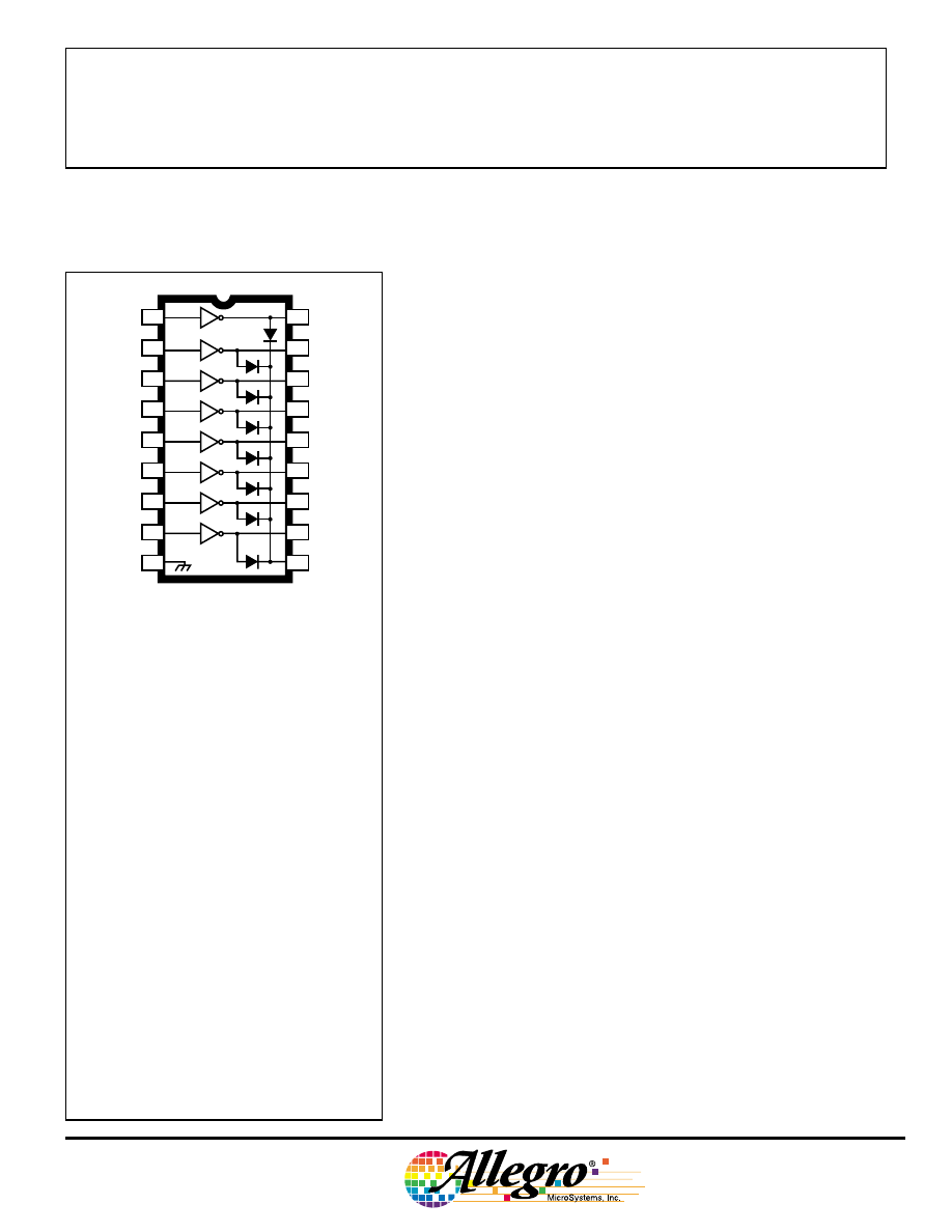
These Darlington arrays are furnished in 18-pin dual in-line
plastic packages (suffix ‘A’) or 18-lead small-outline plastic packages
(suffix ‘LW’). All devices are pinned with outputs opposite inputs to
facilitate ease of circuit board layout. Prefix ‘ULN’ devices are rated
for operation over the temperature range of -20
°
C to +85
°
C; prefix
‘ULQ’ devices are rated for operation to -40
°
C.
x = Character to identify specific device. Characteristic shown applies to family
of devices with remaining digits as shown. See matrix on next page.
2803
THRU
2824
18
17
15
14
13
7
12
8
11
9
10
1
2
4
5
6
Dwg. No. A-10,322A
16
3
ABSOLUTE MAXIMUM RATINGS
Output Voltage, V
CE
(x2803x and x2804x) ..................... 50 V
(x2823x and x2824x) ..................... 95 V
Input Voltage, V
IN
.............................. 30 V
Continuous Output Current, I
C
.... 500 mA
Continuous Input Current, I
IN
....... 25 mA
Power Dissipation, P
D
(one Darlington pair) .................. 1.0 W
(total package) ..................... See Graph
Operating Temperature Range, T
A
Prefix ‘ULN’ .............. -20
°
C to + 85
°
C
Prefix ‘ULQ’ ............... -40
°
C to +85
°
C
Storage Temperature Range,
T
S
................................ -55
°
C to +150
°
C
Note that the ULx28xxA series (dual in-line
package) and ULx28xxLW series (small-
outline IC package) are electrically identical
and share a common terminal number assign-
ment.
The ULx2804, ULx2823, & ULx2824 are discontinued.
Shown for reference only.
2803
THRU
2824
HIGH-VOLTAGE,
HIGH-CURRENT
DARLINGTON ARRAYS
115 Northeast Cutoff, Box 15036
Worcester, Massachusetts 01615-0036 (508) 853-5000
2
ULx28x4A/LW (Each Driver)
Copyright © 1977, 2001 Allegro MicroSystems, Inc.
V
CE(MAX)
50 V
95 V
I
C(MAX)
500 mA
500 mA
Logic
Part Number
5V
ULN2803A*
ULN2823A*
TTL, CMOS
ULN2803LW*
ULN2823LW
6-15 V
ULN2804A*
ULN2824A*
CMOS, PMOS
ULN2804LW*
ULN2824LW
* Also available for operation between -40
°
C and +85
°
C. To order, change
prefix from ‘ULN’ to ‘ULQ’.
DEVICE PART NUMBER DESIGNATION
50
75
100
125
150
2.5
0.5
0
AMBIENT TEMPERATURE IN
°°°°
C
2.0
1.5
1.0
25
Dwg. GP-018B
SUFFIX 'A', R = 60
°
C/W
θ
JA
SUFFIX 'LW', R = 80
°
C/W
θ
JA
ALLOWABLE PACKAGE POWER DISSIPATION IN WATTS
ULx28x3A/LW (Each Driver)
PARTIAL SCHEMATICS
x = Character to identify specific device. Specification shown applies to
family of devices with remaining digits as shown. See matrix above.
The ULx2804, ULx2823, & ULx2824 are discontinued.
Shown for reference only.
Dwg. FP-052-2
3 K
7.2 K
2.7 K
Dwg. FP-052-3
3 K
7.2 K
10.5 K
2803
THRU
2824
HIGH-VOLTAGE,
HIGH-CURRENT
DARLINGTON ARRAYS
www.allegromicro.com
3
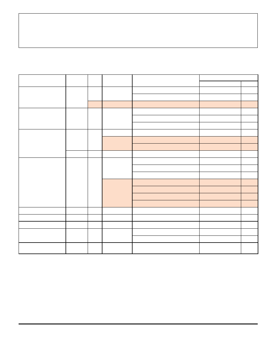
Test
Applicable
Limits
Characteristic
Symbol
Fig.
Devices
Test Conditions
Min.
Typ.
Max.
Units
Output Leakage Current
I
CEX
1A
All
V
CE
= 50 V, T
A
= 25
°
C
—
< 1
50
µ
A
V
CE
= 50 V, T
A
= 70
°
C
—
< 1
100
µ
A
1B
ULx2804x
V
CE
= 50 V, T
A
= 70
°
C, V
IN
= 1.0 V
—
< 5
500
µ
A
Collector-Emitter
V
CE(SAT)
2
All
I
C
= 100 mA, I
B
= 250
µ
A
—
0.9
1.1
V
Saturation Voltage
l
C
= 200 mA, I
B
= 350
µ
A
—
1.1
1.3
V
I
C
= 350 mA, I
B
= 500
µ
A
—
1.3
1.6
V
Input Current
I
IN(ON)
3
ULx2803x
V
IN
= 3.85 V
—
0.93
1.35
mA
ULx2804x
V
IN
= 5.0 V
—
0.35
0.5
mA
V
IN
= 12 V
—
1.0
1.45
mA
I
IN(OFF)
4
All
l
C
= 500
µ
A, T
A
= 70
°
C
50
65
—
µ
A
Input Voltage
V
IN(ON)
5
ULx2803x
V
CE
= 2.0 V, l
C
= 200 mA
—
—
2.4
V
V
CE
= 2.0 V, I
C
= 250 mA
—
—
2.7
V
V
CE
= 2.0 V, l
C
= 300 mA
—
—
3.0
V
ULx2804x
V
CE
= 2.0 V, l
C
= 125 mA
—
—
5.0
V
V
CE
= 2.0 V, l
C
= 200 mA
—
—
6.0
V
V
CE
= 2.0 V, I
C
= 275 mA
—
—
7.0
V
V
CE
= 2.0 V, l
C
= 350 mA
—
—
8.0
V
Input Capacitance
C
IN
—
All
—
15
25
pF
Turn-On Delayt
PLH
8
All
0.5 E
IN
to 0.5 E
OUT
—
0.25
1.0
µ
s
Turn-Off Delayt
PHL
8
All
0.5 E
IN
to 0.5 E
OUT
—
0.25
1.0
µ
s
Clamp Diode
I
R
6
All
V
R
= 50 V, T
A
= 25
°
C
—
—
50
µ
A
Leakage Current
V
R
= 50 V, T
A
= 70
°
C
—
—
100
µ
A
Clamp Diode
V
F
7
All
I
F
= 350 mA
—
1.7
2.0
V
Forward Voltage
Complete part number includes prefix to operating temperature range: ULN = -20
°
C to +85
°
C, ULQ = -40
°
C to +85
°
C
and a suffix to identify package style: A = DIP, LW = SOIC.
Types ULx2803A, ULx2803LW, ULx2804A, and ULx2804LW
ELECTRICAL CHARACTERISTICS at +25
°
C (unless otherwise noted).
The ULx2804 is discontinued.
Shown for reference only.
2803
THRU
2824
HIGH-VOLTAGE,
HIGH-CURRENT
DARLINGTON ARRAYS
115 Northeast Cutoff, Box 15036
Worcester, Massachusetts 01615-0036 (508) 853-5000
4
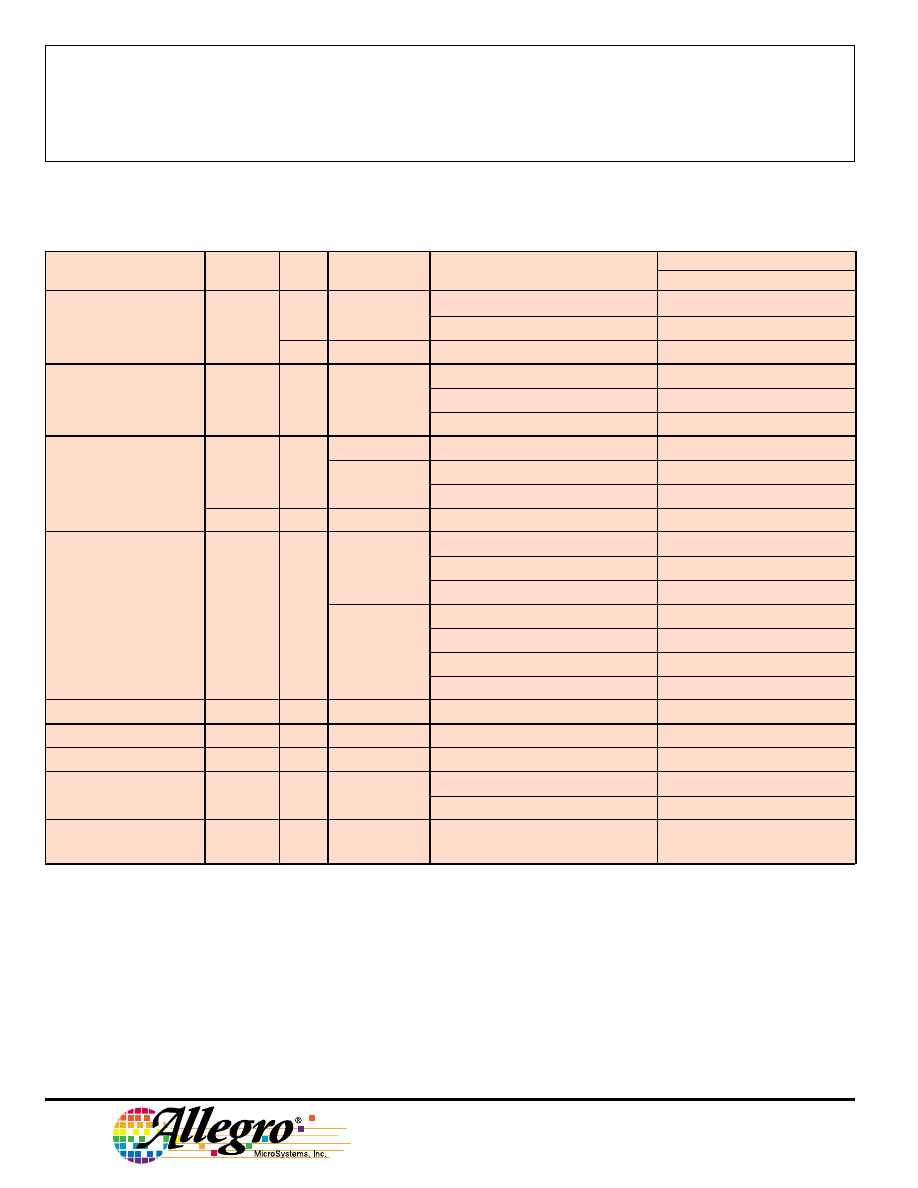
Test
Applicable
Limits
Characteristic
Symbol
Fig.
Devices
Test Conditions
Min.
Typ.
Max.
Units
Output Leakage Current
I
CEX
1A
All
V
CE
= 95 V, T
A
= 25
°
C
—
< 1
50
µ
A
V
CE
= 95 V, T
A
= 70
°
C
—
< 1
100
µ
A
1B
ULx2824x
V
CE
= 95 V, T
A
= 70
°
C, V
IN
= 1.0 V
—
< 5
500
µ
A
Collector-Emitter
V
CE(SAT)
2
All
I
C
= 100 mA, I
B
= 250
µ
A
—
0.9
1.1
V
Saturation Voltage
l
C
= 200 mA, I
B
= 350
µ
A
—
1.1
1.3
V
I
C
= 350 mA, I
B
= 500
µ
A
—
1.3
1.6
V
Input Current
I
IN(ON)
3
ULx2823x
V
IN
= 3.85 V
—
0.93
1.35
mA
ULx2824x
V
IN
= 5.0 V
—
0.35
0.5
mA
V
IN
= 12 V
—
1.0
1.45
mA
I
IN(OFF)
4
All
l
C
= 500
µ
A, T
A
= 70
°
C
50
65
—
µ
A
Input Voltage
V
IN(ON)
5
ULx2823x
V
CE
= 2.0 V, l
C
= 200 mA
—
—
2.4
V
V
CE
= 2.0 V, I
C
= 250 mA
—
—
2.7
V
V
CE
= 2.0 V, l
C
= 300 mA
—
—
3.0
V
ULx2824x
V
CE
= 2.0 V, l
C
= 125 mA
—
—
5.0
V
V
CE
= 2.0 V, l
C
= 200 mA
—
—
6.0
V
V
CE
= 2.0 V, I
C
= 275 mA
—
—
7.0
V
V
CE
= 2.0 V, l
C
= 350 mA
—
—
8.0
V
Input Capacitance
C
IN
—
All
—
15
25
pF
Turn-On Delayt
PLH
8
All
0.5 E
IN
to 0.5 E
OUT
—
0.25
1.0
µ
s
Turn-Off Delayt
PHL
8
All
0.5 E
IN
to 0.5 E
OUT
—
0.25
1.0
µ
s
Clamp Diode
I
R
6
All
V
R
= 95 V, T
A
= 25
°
C
—
—
50
µ
A
Leakage Current
V
R
= 95 V, T
A
= 70
°
C
—
—
100
µ
A
Clamp Diode
V
F
7
All
I
F
= 350 mA
—
1.7
2.0
V
Forward Voltage
Complete part number includes prefix to operating temperature range: ULN = -20
°
C to +85
°
C, ULQ = -40
°
C to +85
°
C
and a suffix to identify package style: A = DIP, LW = SOIC. Note that the ULQ2823LW and ULQ2824LW are not presently
available.
Types ULx2823A, ULN2823LW, ULx2824A, and ULN2824LW
ELECTRICAL CHARACTERISTICS at +25
°
C (unless otherwise noted).
The ULx2823 & ULx2824 are discontinued.
Shown for reference only.
2803
THRU
2824
HIGH-VOLTAGE,
HIGH-CURRENT
DARLINGTON ARRAYS
www.allegromicro.com
5
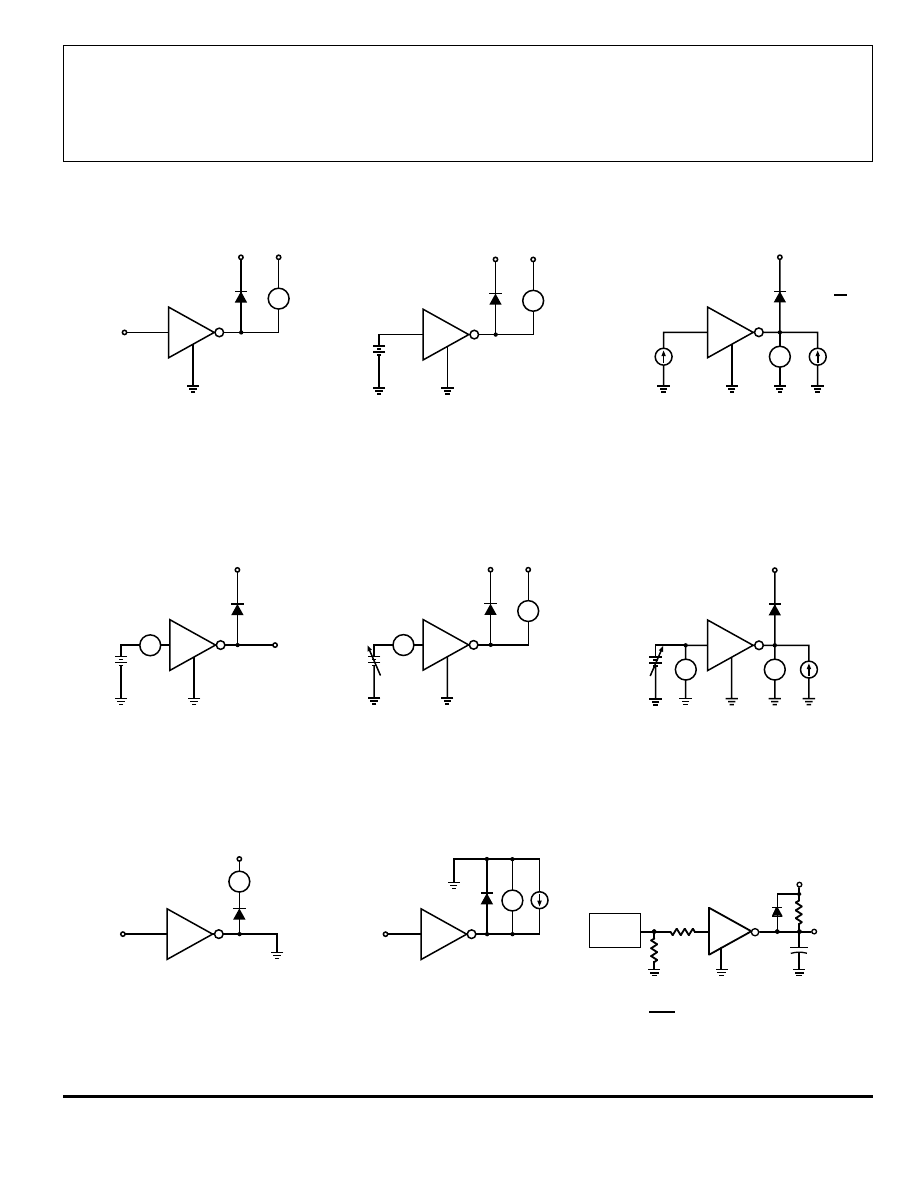
TEST FIGURES
Dwg. No. A-9732A
Dwg. No. A-9733A
Dwg. No. A-9734A
FIGURE 6
FIGURE 7
FIGURE 8
Dwg. No. A-9735A
Dwg. No. A-9736A
V
in
ULx28x3x
3.5 V
ULx28x4x
12 V
FIGURE 1A
FIGURE 1B
FIGURE 2
FIGURE 3
FIGURE 4
FIGURE 5
Dwg. No. A-9731A
Dwg. No. A-9730A
Dwg. No. A-9729A
OPEN
OPEN
VCE
ICEX
µ
A
VIN
OPEN
VCE
ICEX
µ
A
IB
OPEN
hFE =
VCE
V
IC
IB
IC
VIN
OPEN
mA
OPEN
IIN
OPEN
VCE
IC
µ
A
IIN
µ
A
V
OPEN
VCE
V
VIN
IC
OPEN
VR
IR
µ
A
IF
OPEN
VF
V
PULSE
GENERATOR
PRR = 10 kHz
DC = 50 %
INPUT
93
Ω
100
Ω
50 pF
30
Ω
OUT
+50 V
Dwg. EP-072
2803
THRU
2824
HIGH-VOLTAGE,
HIGH-CURRENT
DARLINGTON ARRAYS
115 Northeast Cutoff, Box 15036
Worcester, Massachusetts 01615-0036 (508) 853-5000
6
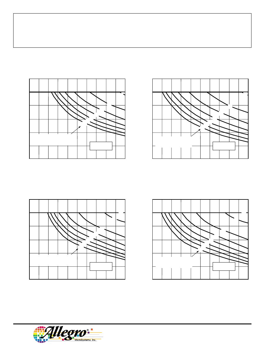
20
Dwg. GP-070-4
40
100
80
DUTY CYCLE IN PER CENT
0
600
400
OUTPUT CURRENT IN mA/CHANNEL
200
0
60
NUMBER OF OUTPUTS
CONDUCTING
SIMULTANEOUSLY
T
A
= +50
°
C
R
θ
JA
= 80
°
C/W
2
3
4
5
6
8
7
20
Dwg. GP-070-3
40
100
80
DUTY CYCLE IN PER CENT
0
600
400
OUTPUT CURRENT IN mA/CHANNEL
200
0
60
NUMBER OF OUTPUTS
CONDUCTING
SIMULTANEOUSLY
1
T
A
= +70
°
C
R
θ
JA
= 80
°
C/W
8
3
4
6
7
5
2
ALLOWABLE COLLECTOR CURRENT
AS A FUNCTION OF DUTY CYCLE
ULx28xxLW
20
Dwg. GP-070-2
40
100
80
DUTY CYCLE IN PER CENT
0
600
400
OUTPUT CURRENT IN mA/CHANNEL
200
0
60
NUMBER OF OUTPUTS
CONDUCTING
SIMULTANEOUSLY
T
A
= +50
°
C
R
θ
JA
= 60
°
C/W
2
3
4
5
6
8
7
20
Dwg. GP-070-1
40
100
80
DUTY CYCLE IN PER CENT
0
600
400
OUTPUT CURRENT IN mA/CHANNEL
200
0
60
NUMBER OF OUTPUTS
CONDUCTING
SIMULTANEOUSLY
1
T
A
= +70
°
C
R
θ
JA
= 60
°
C/W
8
3
4
6
7
5
2
ALLOWABLE COLLECTOR CURRENT
AS A FUNCTION OF DUTY CYCLE
ULx28xxA
x = Characters to identify specific device. Specification shown applies to family of devices with remaining digits as shown.
2803
THRU
2824
HIGH-VOLTAGE,
HIGH-CURRENT
DARLINGTON ARRAYS
www.allegromicro.com
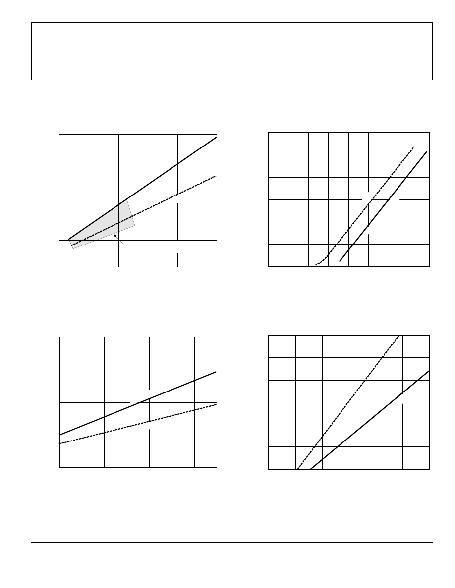
7
INPUT CURRENT AS A
FUNCTION OF INPUT VOLTAGE
ULx28x3x
3.0
Dwg. GP-069
5.0
6.0
INPUT VOLTAGE
2.0
2.5
2.0
INPUT CURRENT IN mA — I
IN
1.0
0
MAXIMUM
0.5
1.5
4.0
AREA OF NORMAL OPERATION
WITH STANDARD OR SCHOTTKY TTL
TYPICAL
0.5
Dwg. GP-067
1.0
2.0
1.5
COLLECTOR-EMITTER SATURATION VOLTAGE
0
600
400
COLLECTOR CURRENT IN mA
200
0
TYPICAL
MAX. SATURATION VOLTAGE
COLLECTOR CURRENT AS A
FUNCTION OF INPUT CURRENT
200
Dwg. GP-068
400
600
INPUT CURRENT IN
µµµµ
A
0
600
400
COLLECTOR CURRENT IN mA
200
0
MAX. REQ'D INPUT CURRENT
TYPICAL
ULx28x4x
6
Dwg. GP-069-1
10
12
INPUT VOLTAGE
5
2.0
INPUT CURRENT IN mA
—
I
IN
1.0
0
MAXIMUM
0.5
1.5
8
TYPICAL
7
9
11
SATURATION VOLTAGE AS A FUNCTION OF
COLLECTOR CURRENT
x = Characters to identify specific device. Characteristic shown applies to family of devices with remaining digits as shown.
2803
THRU
2824
HIGH-VOLTAGE,
HIGH-CURRENT
DARLINGTON ARRAYS
115 Northeast Cutoff, Box 15036
Worcester, Massachusetts 01615-0036 (508) 853-5000
8
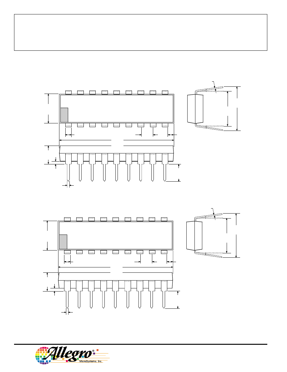
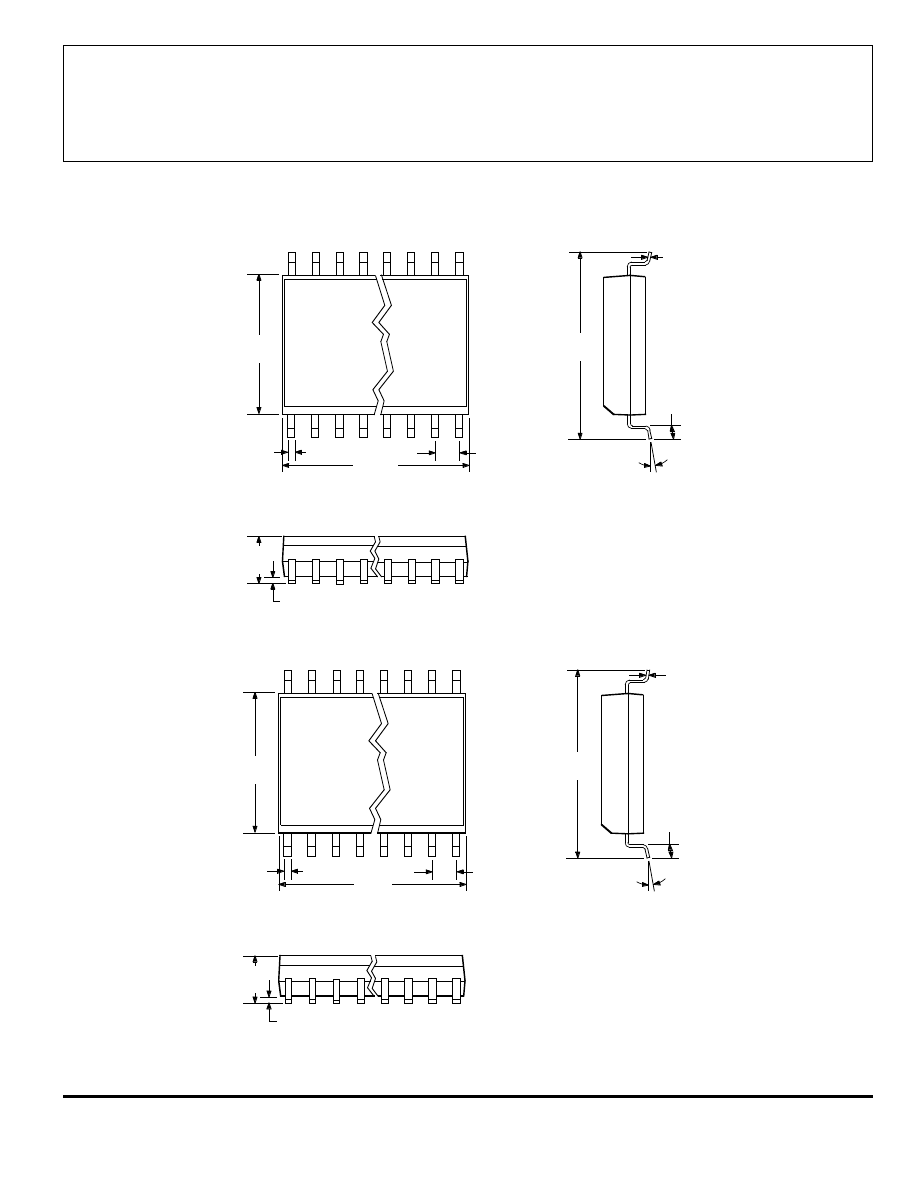
PACKAGE DESIGNATOR “A” DIMENSIONS
Dimensions in Inches
(controlling dimensions)
Dimensions in Millimeters
(for reference only)
NOTES: 1. Exact body and lead configuration at vendor’s option within limits shown.
2. Lead spacing tolerance is non-cumulative.
3. Lead thickness is measured at seating plane or below.
0.014
0.008
0.300
BSC
Dwg. MA-001-18A in
0.430
MAX
18
1
9
0.280
0.240
0.210
MAX
0.070
0.045
0.015
MIN
0.022
0.014
0.100
BSC
0.005
MIN
0.150
0.115
10
0.920
0.880
0.355
0.204
7.62
BSC
Dwg. MA-001-18A mm
10.92
MAX
18
1
9
7.11
6.10
5.33
MAX
1.77
1.15
0.39
MIN
0.558
0.356
2.54
BSC
0.13
MIN
3.81
2.93
10
23.37
22.35
2803
THRU
2824
HIGH-VOLTAGE,
HIGH-CURRENT
DARLINGTON ARRAYS
www.allegromicro.com
9
PACKAGE DESIGNATOR “LW” DIMENSIONS
Dimensions in Inches
(for reference only)
Dimensions in Millimeters
(controlling dimensions)
0
°
TO
8
°
1
18
2
3
0.51
0.33
0.10
MIN.
0.32
0.23
1.27
0.40
Dwg. MA-008-18A mm
1.27
BSC
10
7.60
7.40
10.65
10.00
11.75
11.35
2.65
2.35
0
°
TO
8
°
1
2
3
0.020
0.013
0.0040
MIN.
0.0125
0.0091
0.050
0.016
wg. MA-008-18A in
0.050
BSC
18
10
0.419
0.394
0.2992
0.2914
0.4625
0.4469
0.0926
0.1043
NOTES: 1. Exact body and lead configuration at vendor’s option within limits shown.
2. Lead spacing tolerance is non-cumulative.

2803
THRU
2824
HIGH-VOLTAGE,
HIGH-CURRENT
DARLINGTON ARRAYS
115 Northeast Cutoff, Box 15036
Worcester, Massachusetts 01615-0036 (508) 853-5000
10
The products described here are manufactured under one or more
U.S. patents or U.S. patents pending.
Allegro MicroSystems, Inc. reserves the right to make, from time to
time, such departures from the detail specifications as may be required
to permit improvements in the performance, reliability, or
manufacturability of its products. Before placing an order, the user is
cautioned to verify that the information being relied upon is current.
Allegro products are not authorized for use as critical components
in life-support devices or systems without express written approval.
The information included herein is believed to be accurate and
reliable. However, Allegro MicroSystems, Inc. assumes no responsi-
bility for its use; nor for any infringement of patents or other rights of
third parties which may result from its use.
Wyszukiwarka
Podobne podstrony:
2801
2801
2801 Transfer case fluid change
więcej podobnych podstron