Abstract—This paper presents a new digital control strategy
of a three-phase PWM inverter for Uninterruptible Power
Supplies (UPS) systems. To achieve a fast transient response, a
good voltage regulation, nearly zero steady state inverter output
voltage error, and low total harmonic distortion (THD), the
proposed control method consists of two discrete-time feedback
controllers:
a discrete-time optimal + sliding-mode voltage
controller in outer loop and a discrete-time optimal current
controller in inner loop. To prove the effectiveness of the
proposed technique, various simulation results using
Matlab/Simulink are shown under both linear and nonlinear
loads.
Index Terms—digital control, optimal control, sliding-mode
control, space vector PWM, uninterruptible power supplies.
I. I
NTRODUCTION
In order to deliver a good ac power during emergency, the
UPS systems that include the feedback controlled
pulse-width modulated (PWM) inverter and L-C output filter
have to convert a dc voltage source (batteries) to a sinusoidal
ac voltage with low steady state voltage error, low voltage
THD, and fast transient response under load disturbances.
Furthermore, the good performance mentioned above should
be guaranteed under power pollution which leads to voltage
distortion due to increasing applications of power converters
or nonlinear loads in industry.
Recently, techniques to produce an output voltage with
low total harmonic distortion (THD) in a three-phase pulse
width modulation (PWM) inverter have been proposed [1-4].
Even if real-time deadbeat controllers [1-3] have low THD
for linear load and a fast transient response for load
disturbances, it is known that they are sensitive to parametric
variations and model uncertainties as well as these techniques
have a high THD under nonlinear load. On the other hand,
discrete-time optimal voltage/current controllers in a rotating
reference frame have been proposed for UPS applications of
three-phase PWM inverter [4]. However, it does not consider
a nonlinear load. Thus, a new controller is needed for the
good performance such as nearly zero steady state inverter
output voltage error, low THD, good voltage regulation,
robustness, fast transient response, and protection of the
inverter against overload under linear/nonlinear loads.
In this paper, a new control strategy employing two
discrete-time optimal controllers where good performance
stated previously is guaranteed by the proper choice of the
weighting matrices of two linear quadratic regulators is
proposed for the three-phase UPS systems under both linear
and nonlinear loads. First of all, the proposed control scheme
is easily implemented based on a discrete-time state space
equation given by modeling of the given plant system.
Particularly, the discrete-time optimal voltage controller
includes a sliding-mode control model because of its
characteristics such as the good transient and no-overshoot
response.
First, a circuit model of the three-phase UPS system and a
discrete-time state space equation are given in a stationary qd
reference frame. Next, two discrete-time state feedback
controllers are designed: a discrete-time optimal +
sliding-mode voltage controller in outer loop and a
discrete-time optimal current controller in inner loop. Also,
Space Vector Pulse-Width Modulation (SVPWM) is chosen
as a technique of PWM to perform this algorithm. To verify
our proposed method, various simulation results using
Matlab/Simulink are presented under linear/nonlinear loads.
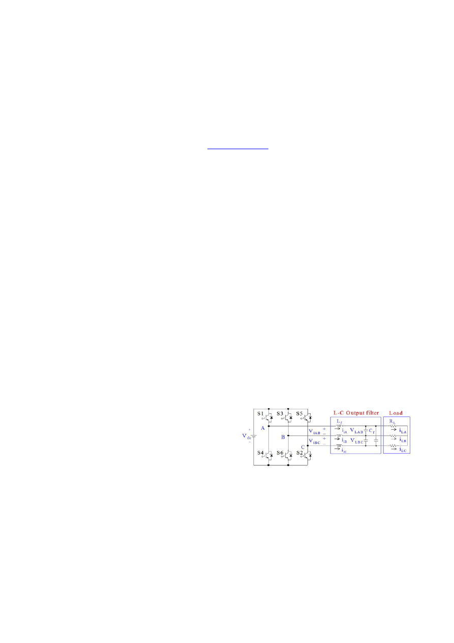
II.
UPS
S
YSTEM
M
ODELING
Fig. 1 illustrates a circuit model of the UPS system, and the
system consists of a DC voltage source (V
dc
), a three-phase
voltage source PWM inverter, L-C inverter output filter (L
f
,
C
f
), and a load (R
L
).
The circuit model described in Fig. 1 uses the following
quantities. The inverter output line-to-line voltage is
represented by the vector V
i
= [V
iAB
V
iBC
V
iCA
]
T
, and the
three-phase inverter output currents are i
iA
, i
iB
, and i
iC
. Based
on these currents, a vector is defined as I
i
= [i
iAB
i
iBC
i
iCA
]
T
=
[i
iA
-i
iB
i
iB
-i
iC
i
iC
-i
iA
]
T
. Also, the line to line load voltage and
phase load current vectors can be represented by V
L
= [V
LAB
V
LBC
V
LCA
]
T
and I
L
= [i
LA
i
LB
i
LC
]
T
, respectively.
On the L-C output filter, the following current and voltage
Optimal Control of Three-Phase PWM Inverter for UPS Systems
J. W. Jung, M. Dai, A. Keyhani, Fellow, IEEE
Department of Electrical and Computer Engineering
The Ohio State University, Columbus, OH43210, USA
Phone: +1 – 614 – 292 – 4430; Fax: +1 – 614 – 292 – 7596
Email:
keyhani.1@osu.edu
Fig. 1. UPS system circuit model.
2004 35th Annual IEEE Power Electronics Specialists Conference
Aachen, Germany, 2004
0-7803-8399-0/04/$20.00 ©2004 IEEE.
2054
equations are obtained after elementary calculation:
i). Current equations:
(
)
(
)
(
)
⎪
⎪
⎪
⎪
⎩
⎪⎪
⎪
⎪
⎨
⎧
−
−
=
−
−
=
−
−
=
LA
LC
f
iCA
f
LCA
LC
LB
f
iBC
f
LBC
LB
LA
f
iAB
f
LAB
i
i
C
i
C
dt
dV
i
i
C
i
C
dt
dV
i
i
C
i
C
dt
dV
3
1
3
1
3
1
3
1
3
1
3
1
. (1)
ii). Voltage equations:
⎪
⎪
⎪
⎩
⎪
⎪
⎪
⎨
⎧
+
−
=
+
−
=
+
−
=
iCA
f
LCA
f
iCA
iBC
f
LBC
f
iBC
iAB
f
LAB
f
iAB
V
L
V
L
dt
di
V
L
V
L
dt
di
V
L
V
L
dt
di
1
1
1
1
1
1
. (2)
Rewrite (1) and (2) into a vector form, respectively:
i
f
L
f
i
L
i
f
i
f
L
L
L
dt
d
C
C
dt
d
V
V
I
I
T
I
V
1
1
3
1
3
1
+
−
=
−
=
, (3)
where,
⎥
⎥
⎥
⎦
⎤
⎢
⎢
⎢
⎣
⎡
−
−
−
=
1
0
1
1
1
0
0
1
1
i
T
.
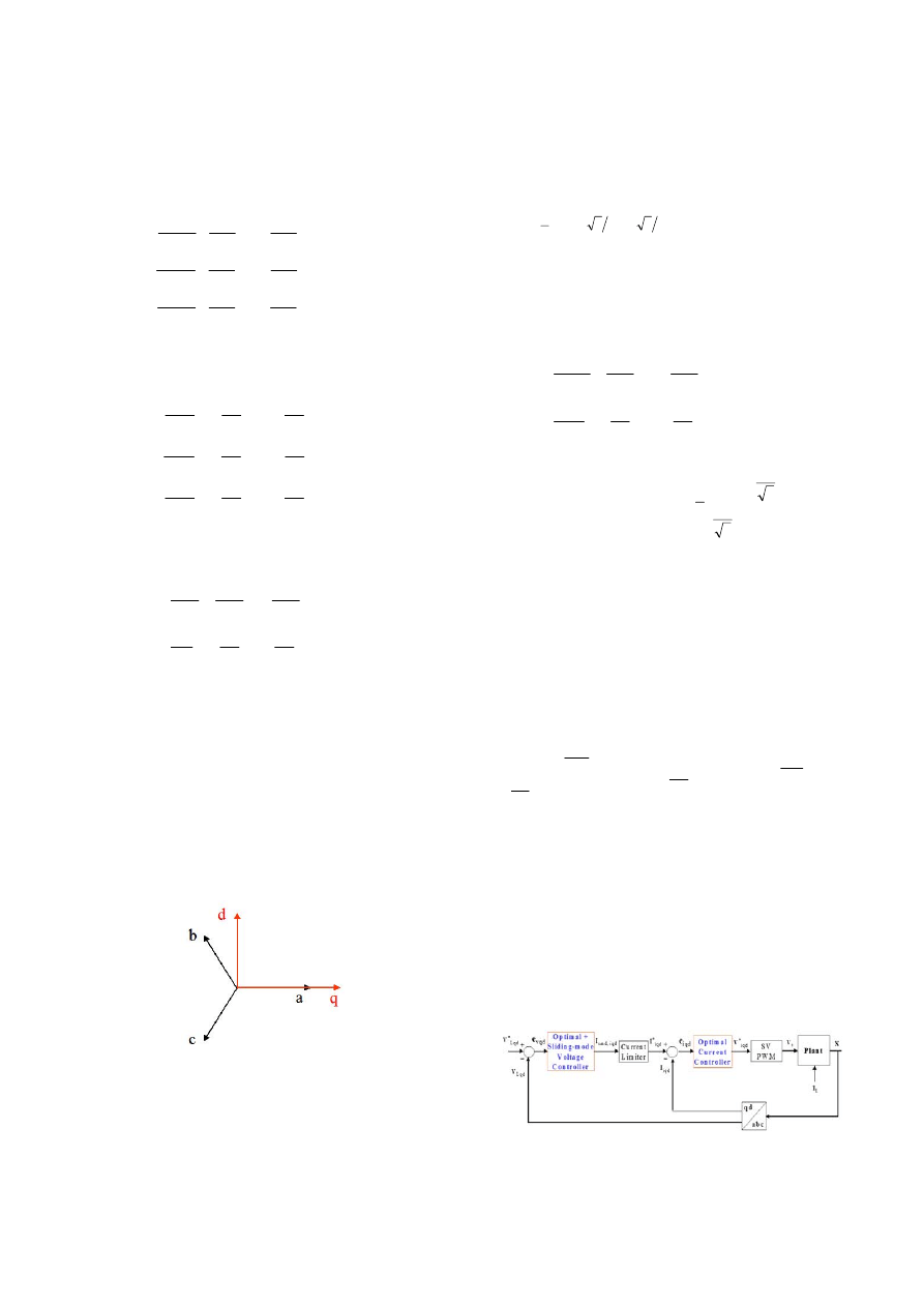
To implement space vector PWM, the above state
equations (3) can be transformed from the abc reference
frame into the stationary qd reference frame that consists of
the horizontal (q) and vertical (d) axes. Fig. 2 shows the
relationship between the abc reference frame and stationary
qd reference frame.
Based on Fig. 2, the Clarke transformation which outputs a
two coordinate time-varying system (i.e., the q-axis leads the
d-axis by 90
°) is given by (4)
abc
s
qd
f
K
f
=
0
, (4)
T
c
b
a
abc
T
d
q
qd
f
f
f
f
f
f
]
[
,
]
[
,
2
/
1
2
/
1
2
/
1
2
3
2
3
0
2
/
1
2
/
1
1
3
2
where,
0
0
s
=
=
⎥
⎥
⎥
⎦
⎤
⎢
⎢
⎢
⎣
⎡
−
−
−
=
f
f
K
and f denotes either a voltage or a current variable.
By applying (4) to (3), transform the state equations (3) to the
stationary qd reference frame below:
iqd
f
Lqd
f
iqd
Lqd
iqd
f
iqd
f
Lqd
L
L
dt
d
C
C
dt
d
V
V
I
I
T
I
V
1
1
3
1
3
1
+
−
=
−
=
, (5)
⎥
⎥
⎥
⎥
⎦
⎤
⎢
⎢
⎢
⎢
⎣
⎡
−
=
=
−
1
3
1
3
1
1
2
3
]
[
,
where
2
,
1
,
,
1
column
row
s
i
s
iqd
K
T
K
T
.
Also, we assume that the L
f
and C
f
parameters in the
network are constant, and then the given plant model (5) can
be expressed as the following continuous-time state space
equation for a linear time-invariant (LTI) system
)
(
)
(
)
(
)
(
t
t
t
t
Ed
Bu
AX
X
+
+
=
&
, (6)
where,
1
4
×
⎥
⎥
⎦
⎤
⎢
⎢
⎣
⎡
=
iqd
Lqd
I
V
X
,
1
2
]
[
×
=
iqd
V
u
,
1
2
]
[
×
=
Lqd
I
d
,
4
4
2
2
2
2
2
2
2
2
0
1
3
1
0
×
×
×
×
×
⎥
⎥
⎥
⎥
⎦
⎤
⎢
⎢
⎢
⎢
⎣
⎡
−
=
I
L
I
C
f
f
A
,
2
4
2
2
2
2
1
0
×
×
×
⎥
⎥
⎥
⎦
⎤
⎢
⎢
⎢
⎣
⎡
=
I
L
f
B
,
2
4
2
2
0
3
1
×
×
⎥
⎥
⎥
⎦
⎤
⎢
⎢
⎢
⎣
⎡−
=
iqd
f
C
T
E
.
Note that the line to line load voltage V
Lqd
and inverter
output current I
iqd
are the state variables of the system, the
inverter output line-to-line voltage V
iqd
is the control input
(u), and the load current I
Lqd
is defined as the disturbance (d).
III. C
ONTROL
S
YSTEM
D
ESIGN
Fig. 3 shows a block diagram of the total control system
proposed for digital control of the three-phase PWM inverter
for UPS systems.
Fig. 2. Relationship between the abc reference frame and the
stationary qd reference frame.
Fig. 3. Block diagram of total control system.
2004 35th Annual IEEE Power Electronics Specialists Conference
Aachen, Germany, 2004
2055
In Fig. 3, the proposed control system consists of two
feedback controllers: a discrete-time optimal + sliding mode
controller is used in the outer loop for voltage control, while a
discrete-time optimal controller is in the inner loop for
current regulation [5-7]. Design of each controller will be
described in the following section in detail.
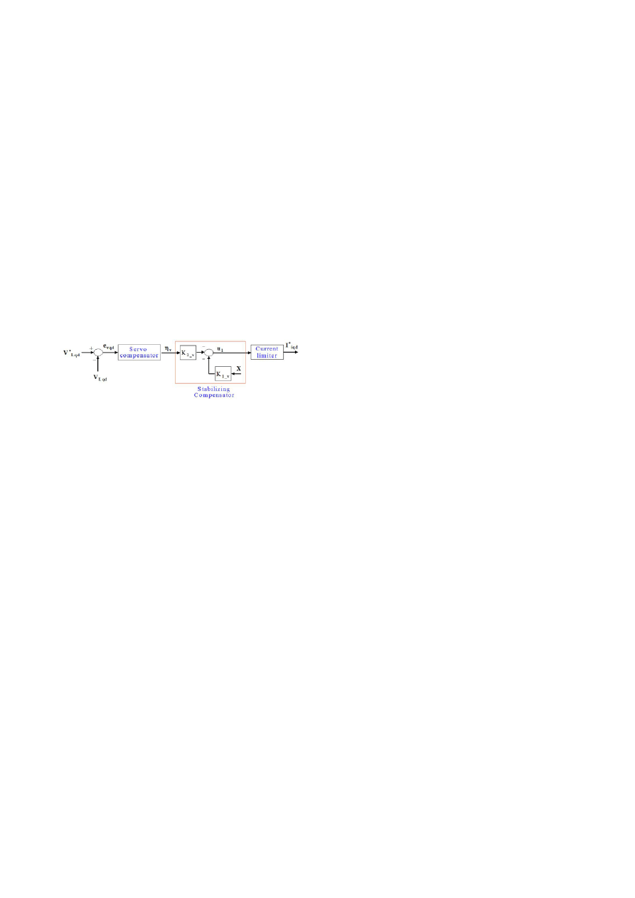
A. Voltage Controller in the outer loop
As shown in Fig. 4, a discrete-time voltage controller based
on a discrete-time robustness servomechanism controller
(RSC) that consists of a servo-compensator and a stabilizing
compensator is used for voltage regulation in an outer loop.
Furthermore, dynamics of a discrete-time sliding-mode
control (DSMC) is combined with the given plant model
because of the fast and no-overshoot response it provides [7].
Next, the current command signal (I
cmd,iqd
) is limited by
maximum current predetermined to protect the system under
overload.
The goal of designing a realistic multivariable controller to
solve the robust servomechanism problem (RSP) is to
achieve closed-loop stability and asymptotic regulation as
well as fast response and robustness. In this paper, a
discrete-time robustness servomechanism controller (RSC)
that combines both the internal model principle and the
optimal control theory is adopted for voltage control due to
its capability to perform zero steady state tracking error under
unknown load and to eliminate harmonics of any specified
frequencies with guaranteed system stability [5-6].
The continuous-time state space equation (6) of the plant
system can be expressed to include dynamics of DSMC
below:
⎩
⎨
⎧
=
+
+
=
)
(
)
(
)
(
)
(
)
(
)
(
1
1
t
t
t
t
t
t
X
C
y
Ed
Bu
AX
X&
, (7)
where,
]
[
1
iqd
I
y
=
,
⎥
⎦
⎤
⎢
⎣
⎡
=
1
0
0
0
0
1
0
0
1
C
.
Given the sampling period T
z
, the (7) can be transformed to
the following discrete-time state space equation:
⎩
⎨
⎧
=
+
+
=
+
)
(
)
(
)
(
)
(
)
(
)
1
(
1
1
*
*
*
k
k
k
k
k
k
X
C
y
d
E
u
B
X
A
X
, (8)
where,
z
T
e
A
A
=
*
,
∫
−
=
z
z
T
T
d
e
0
)
(
*
τ
τ
B
B
A
,
∫
−
=
z
z
T
T
d
e
0
)
(
*
τ
τ
E
E
A
.
In order to control the output y
1
(k) to follow the reference
y
1
_
ref
(k), a sliding mode manifold may be selected in the form
of
)
(
)
(
)
(
)
(
)
(
_
1
1
_
1
1
k
k
k
k
k
ref
ref
y
X
C
y
y
s
−
=
−
=
, (9)
where, y
1
_
ref
(k) = I
cmd,iqd
(k).
In other words, when the discrete-time sliding mode exists,
which means s(k) = 0, the output y
1
(k) is identical to the
reference y
1
_
ref
(k). Therefore, the discrete-time sliding mode
exists if the control input u(k) is designed as the solution of:
0
)
1
(
)
(
)
(
)
(
)
1
(
)
1
(
)
1
(
_
1
*
1
*
1
*
1
_
1
1
=
+
−
+
+
=
+
−
+
=
+
k
k
k
k
k
k
k
ref
ref
y
d
E
C
u
B
C
X
A
C
y
y
s
. (10)
The control law that satisfies (10) and yields motion in the
manifold s(k) = 0 is called ‘equivalent control. For the given
system, the equivalent control u
eq
(k) is given as follows:
( ) (
)
)
(
)
(
)
1
(
)
(
*
1
*
1
_
1
1
*
1
k
k
k
k
ref
eq
d
E
C
X
A
C
y
B
C
u
−
−
+
=
−
. (11)
We assume that y
1
_
ref
(k+1)
≅ y
1
_
ref
(k) because y
1
_
ref
(k) is
constant over a sampling period (T
z
) that is much smaller
than a fundamental period (1/60 sec.). As a result, the
equation (11) can be rewritten:
(
) (
)
)
(
)
(
)
(
)
(
*
1
*
1
,
1
*
1
k
k
k
k
iqd
cmd
eq
d
E
C
X
A
C
I
B
C
u
−
−
=
−
. (12)
After the dynamics (12) of the DSMC is included in (8),
the overall plant for the RSC is:
⎩
⎨
⎧
=
+
+
=
+
)
(
)
(
)
(
)
(
)
(
)
1
(
1
k
k
k
k
k
k
v
v
d
d
d
X
C
y
d
E
u
B
X
A
X
, (13)
where,
(
)
*
1
1
*
1
*
*
A
C
B
C
B
A
A
−
−
=
d
,
(
)
1
*
1
*
−
=
B
C
B
B
d
,
(
)
*
1
1
*
1
*
*
E
C
B
C
B
E
E
−
−
=
d
,
[
]
2
2
2
2
0
×
×
= I
v
C
,
)
(
)
(
,
1
k
k
iqd
cmd
I
u
=
,
]
[
Lqd
v
V
y
=
.
For the given system (13), once the existence of the
solution to RSP is verified according to the conditions in [5],
assuming the tracking/disturbance poles are
±j
ω
1
,
± j
ω
2
,
±
j
ω
3
,
… (i.e., representing sinusoidal signals with fundamental
frequency
ω
1
and harmonic frequencies
ω
2
,
ω
3
,
…), the RSC
can be designed in the following.
If the tracking/disturbance poles to be considered are
±j
ω
1
,
± j
ω
2
, and
± j
ω
3
, a continuous-time servo-compensator is
defined as
)
(
)
(
)
(
t
t
t
vqd
c
v
c
v
e
B
η
A
η
+
=
&
,
(14)
Fig. 4. Block diagram of a discrete-time voltage controller.
2004 35th Annual IEEE Power Electronics Specialists Conference
Aachen, Germany, 2004
2056
where,
Lqd
Lqd
vqd
V
V
e
−
=
*
,
12
12
3
2
2
4
4
4
4
2
4
4
4
4
4
4
1
0
0
0
0
0
0
×
×
×
×
×
×
×
⎥
⎥
⎥
⎦
⎤
⎢
⎢
⎢
⎣
⎡
=
c
c
c
c
A
A
A
A
,
2
12
3
2
1
×
⎥
⎥
⎥
⎦
⎤
⎢
⎢
⎢
⎣
⎡
=
c
c
c
c
B
B
B
B
,
4
4
2
2
2
2
2
2
2
2
2
0
0
×
×
×
×
×
⎥
⎦
⎤
⎢
⎣
⎡
⋅
−
=
I
I
i
ci
ω
A
,
2
4
2
2
2
2
0
×
×
×
⎥
⎦
⎤
⎢
⎣
⎡
=
I
ci
B
,
ω
i
(i = 1, 2, 3),
ω
1
=
ω, ω
2
= 5
⋅ω, ω
3
= 7
⋅ω, ω = 2πf, f = 60 Hz.
Note that only the 5
th
and 7
th
harmonics are chosen as the
disturbance poles because the voltage harmonics such as an
odd multiple of 3 and even harmonics are suppressed in a
three-phase inverter and as a consequence the dominant
harmonics are the 5
th
and 7
th
.
Next, a discrete-time servo-compensator is:
)
(
)
(
)
1
(
*
*
k
k
k
vqd
c
v
c
v
e
B
η
A
η
+
=
+
, (15)
where,
z
c
T
c
e
A
A
=
*
and
∫
−
=
z
z
c
T
c
T
c
d
e
0
)
(
*
τ
τ
B
B
A
.
Therefore, an augmented system combining both the new
plant (13) including the dynamics of DSMC and the
servo-compensator (15) can be written as:
)
(
ˆ
)
(
ˆ
)
(
ˆ
)
(
ˆ
ˆ
)
1
(
ˆ
_
ref
_
2
_
1
1
k
k
k
k
k
v
v
v
v
v
v
v
y
E
d
E
u
B
X
A
X
+
+
+
=
+
, (16)
where,
⎥
⎦
⎤
⎢
⎣
⎡
=
)
(
)
(
)
(
ˆ
k
k
k
v
v
η
X
X
,
⎥
⎦
⎤
⎢
⎣
⎡
−
=
*
*
0
ˆ
c
v
c
d
v
A
C
B
A
A
,
⎥
⎦
⎤
⎢
⎣
⎡
=
0
ˆ
d
v
B
B
,
⎥
⎦
⎤
⎢
⎣
⎡
=
0
ˆ
*
_
1
E
E
v
,
⎥
⎦
⎤
⎢
⎣
⎡
=
*
_
2
0
ˆ
c
v
B
E
,
)
(
)
(
,
1
k
k
iqd
cmd
I
u
=
,
)
(
)
(
k
k
Lqd
I
d
=
,
)
(
)
(
*
_
k
k
Lqd
v
ref
V
y
=
.
The stabilizing compensator , which yields the control
input u
1
in (16), ensures the stability of the overall system
including the plant as well as the servo-compensator and
desirable performance of the system through a feedback gain
matrix K
v
which minimizes a discrete linear quadratic
performance index as follows:
)
(
)
(
)
(
ˆ
)
(
ˆ
0
1
1
k
k
k
k
J
k
T
v
v
v
T
v
∑
∞
=
+
=
u
u
X
Q
X
ε
ε
, (17)
where, Q
v
is a symmetrical positive-definite matrix and
ε
v
>0
is a small number, both of which should be selected by the
controller designer.
The feedback gain K
v
can be obtained using Matlab
function dlqr() which solves the algebraic Riccati equation
for the system (16) such that all eigenvalues of matrix
v
v
v
X
A
ˆ
K
ˆ
−
exist inside of unit disc. Assuming the system is a
linear time-invariant (LTI), the feedback gain K
v
is a constant
value calculated by the Matlab function in advance. Thus, the
control input (u
1
) can be taken from the gain K
v
and state
variables (X and
η
v
):
[
]
)
(
)
(
)
(
)
(
)
(
ˆ
)
(
2
_
1
_
2
_
1
_
1
k
k
k
k
k
k
v
v
v
v
v
v
v
v
η
K
X
K
η
X
K
K
X
K
u
−
−
=
⎥
⎦
⎤
⎢
⎣
⎡
−
=
−
=
. (18)
Finally, since the current command signal should be
limited to protect the system against overload, the algorithm
of the current limiter is included in main program as:
⎪
⎩
⎪
⎨
⎧
>
≤
=
max
,
,
,
max
max
,
,
1
)
(
for
)
(
)
(
)
(
for
)
(
)
(
I
k
k
k
I
I
k
k
k
u
iqd
cmd
iqd
cmd
iqd
cmd
iqd
cmd
iqd
cmd
I
I
I
I
I
. (19)
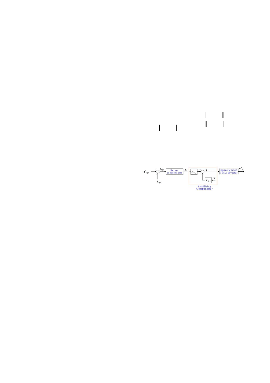
B. Current Controller in inner loop
Similarly, the discrete-time optimal current controller can
also be designed except for the sliding-mode control model
included in the voltage controller.
A discrete form of the plant (6) and the output y
i
(t) is:
⎩
⎨
⎧
=
+
+
=
+
)
(
)
(
)
(
)
(
)
(
)
1
(
*
*
*
k
k
k
k
k
k
i
i
X
C
y
d
E
u
B
X
A
X
, (20)
where,
z
T
e
A
A
=
*
,
∫
−
=
z
z
T
T
d
e
0
)
(
*
τ
τ
B
B
A
,
∫
−
=
z
z
T
T
d
e
0
)
(
*
τ
τ
E
E
A
,
)
(
)
(
*
k
k
iqd
V
u
=
,
[
]
2
2
2
2
0
×
×
=
I
i
C
,
]
[
iqd
i
I
y
=
.
Analogous to the voltage controller, the continuous-time
servo-compensator is defined below
)
(
)
(
)
(
t
t
t
iqd
c
i
c
i
e
B
η
A
η
+
=
&
,
(21)
where,
iqd
iqd
iqd
I
I
e
−
=
*
,
12
12
3
2
2
4
4
4
4
2
4
4
4
4
4
4
1
0
0
0
0
0
0
×
×
×
×
×
×
×
⎥
⎥
⎥
⎦
⎤
⎢
⎢
⎢
⎣
⎡
=
c
c
c
c
A
A
A
A
,
2
12
3
2
1
×
⎥
⎥
⎥
⎦
⎤
⎢
⎢
⎢
⎣
⎡
=
c
c
c
c
B
B
B
B
,
4
4
2
2
2
2
2
2
2
2
2
0
0
×
×
×
×
×
⎥
⎦
⎤
⎢
⎣
⎡
⋅
−
=
I
I
i
ci
ω
A
,
2
4
2
2
2
2
0
×
×
×
⎥
⎦
⎤
⎢
⎣
⎡
=
I
ci
B
,
ω
i
(i = 1, 2, 3),
ω
1
=
ω, ω
2
= 5
⋅ω, ω
3
= 7
⋅ω, ω = 2πf, f = 60 Hz.
Fig. 5. Block diagram of a discrete-time current controller.
2004 35th Annual IEEE Power Electronics Specialists Conference
Aachen, Germany, 2004
2057
Also, note that the 5
th
and 7
th
harmonics are selected as the
dominant disturbance poles like the voltage controller.
By transforming (21) to a discrete form:
)
(
)
(
)
1
(
*
*
k
k
k
iqd
c
i
c
i
e
B
η
A
η
+
=
+
, (22)
where,
z
c
T
c
e
A
A
=
*
and
∫
−
=
z
z
c
T
c
T
c
d
e
0
)
(
*
τ
τ
B
B
A
.
Thus, an augmented system model combining both the
plant (20) and the servo-compensator (22) can be expressed
as follows
)
(
ˆ
)
(
ˆ
)
(
ˆ
)
(
ˆ
ˆ
)
1
(
ˆ
_
ref
_
2
_
1
k
k
k
k
k
i
i
i
i
i
i
i
y
E
d
E
u
B
X
A
X
+
+
+
=
+
, (23)
where,
⎥
⎦
⎤
⎢
⎣
⎡
=
)
(
)
(
)
(
ˆ
k
k
k
i
i
η
X
X
,
⎥
⎦
⎤
⎢
⎣
⎡
−
=
*
*
*
0
ˆ
c
i
c
i
A
C
B
A
A
,
⎥
⎦
⎤
⎢
⎣
⎡
=
0
ˆ
*
B
B
i
,
⎥
⎦
⎤
⎢
⎣
⎡
=
0
ˆ
*
_
1
E
E
i
,
⎥
⎦
⎤
⎢
⎣
⎡
=
*
_
2
0
ˆ
c
i
B
E
,
)
(
)
(
*
k
k
iqd
V
u
=
,
)
(
)
(
k
k
Lqd
I
d
=
,
)
(
)
(
*
_
k
k
iqd
i
ref
I
y
=
.
As described in the voltage controller, the stabilizing
compensator of the current controller, which yields the
optimal control vector u(k) in (23), can guarantee the
stability of the overall system including the plant model as
well as the servo-compensator and the desirable performance
of the system, both of which can be achieved by choosing a
proper feedback gain matrix K
i
that minimizes a discrete
optimization criterion (24) such that the system is stable:
)
(
)
(
)
(
ˆ
)
(
ˆ
0
k
k
k
k
J
k
T
i
i
i
T
i
∑
∞
=
+
=
u
u
X
Q
X
ε
ε
, (24)
where, Q
i
is a symmetrical positive-definite matrix and
ε
i
>0
is a small number, both of which should be selected by the
controller designer.
By solving the Riccati equation for the system (23), the
feedback gain K
i
can be obtained. As a result, the optimal
control input u(k) can be expressed from the gain K
i
and state
variables (X and
η
i
):
[
]
)
(
)
(
)
(
)
(
)
(
ˆ
)
(
2
_
1
_
2
_
1
_
k
k
k
k
k
k
i
i
i
i
i
i
i
i
η
K
X
K
η
X
K
K
X
K
u
−
−
=
⎥
⎦
⎤
⎢
⎣
⎡
−
=
−
=
. (25)
Furthermore, if the control input u(k) can vary within
0
)
(
u
k
≤
u
, then the control input should be limited by the
space vector PWM inverter. So the following modified
control input can be applied:
⎪
⎩
⎪
⎨
⎧
>
≤
=
0
*
*
*
0
0
*
*
)
(
for
)
(
)
(
)
(
for
)
(
)
(
u
k
V
k
V
k
V
u
u
k
V
k
V
k
iqd
iqd
iqd
iqd
iqd
u
, (26)
where,
dc
V
u
3
2
0
=
and the control voltage limit u
0
is also
determined by the SVPWM inverter.
Finally, remark that the feedback gain (K
i-2
) of the
servo-compensator (
η
i
) in the current controller should be at
least ten times larger than the feedback gain (K
v-2
) of the
servo-compensator (
η
v
) in the voltage controller because the
current controller requires much faster response than the
voltage controller.
IV. S
IMULATION
R
ESULTS
To validate the proposed control scheme, digital
simulation has been done under various operating conditions
(both linear and nonlinear loads) using Matlab/Simulink, and
the system parameters are shown in Table 1.
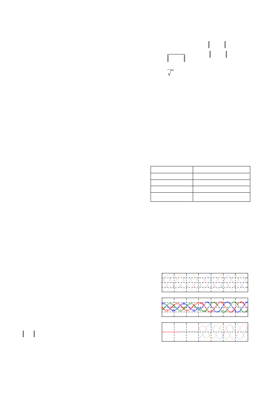
Based on the above system parameters, the various
simulations have been implemented under both linear and
nonlinear loads. In case of the linear load, a resistive load step
change at 80 msec is simulated from 0% to 100% and vice
versa in Fig. 6 and 7, respectively. Next, Fig. 8 shows
simulation results under an inductive load which consists of a
resistor and an inductor. Finally, Fig. 9 shows simulation
waveforms of the nonlinear load which is composed of an
three-phase inductor (2 mH), a three-phase diode bridge, a
DC-link capacitor (1000
µF), and a resistor (7 Ω).
T
ABLE
I
S
YSTEM
P
ARAMETERS
DC Bus Voltage
V
dc
= 360 V
Output Power Rating
P
out
= 10 kVA
AC Output Voltage
V
L, RMS
= 208 V (L-L), f = 60 Hz
Inverter Filters
L
f
= 600
µH, C
f
= 200
µF
Switching (Sampling)
Frequency
f
z
= 5.4 kHz
0.05
0.06
0.07
0.08
0.09
0.1
0.11
0.12
-400
-200
0
200
400
V
LA
B
, V
LB
C
, V
LC
A
[V
]
0.05
0.06
0.07
0.08
0.09
0.1
0.11
0.12
-100
-50
0
50
100
i
iA
, i
iB
, i
iC
[A
]
0.05
0.06
0.07
0.08
0.09
0.1
0.11
0.12
-50
0
50
Time [sec.]
i
LA
, i
LB
, i
LC
[A
]
Fig. 6. Simulation results under a resistive load step change
at 80 msec. (0% to 100%).
2004 35th Annual IEEE Power Electronics Specialists Conference
Aachen, Germany, 2004
2058
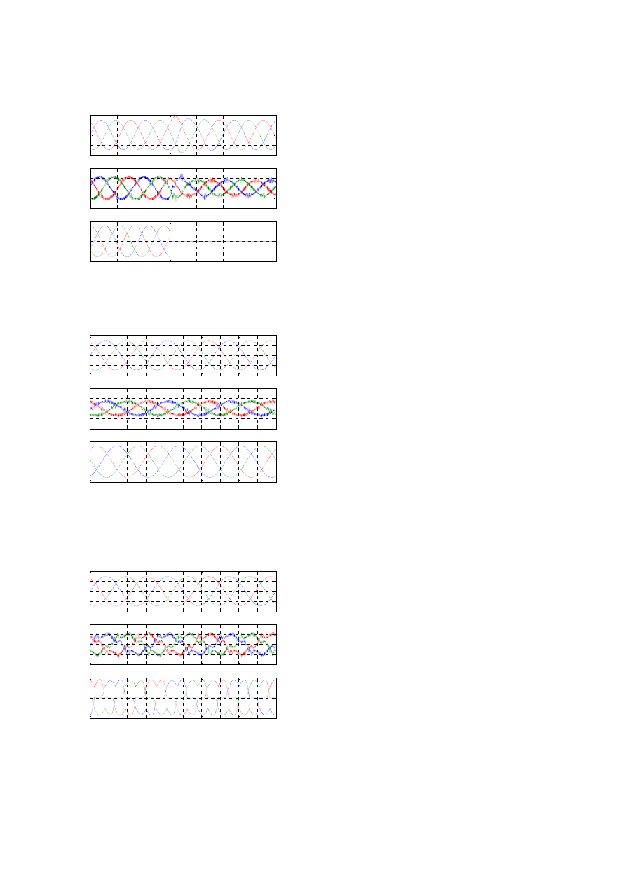
From Fig. 6 to 9, an upper figure shows the load line to line
voltages (V
LAB
, V
LBC
, V
LCA
), a middle one is the inverter
output phase currents (i
iA
,
i
iB
, i
iC
), and a bottom one presents
the load phase currents (i
LA
, i
LB
, i
LC
), respectively.
V.
C
ONCLUSIONS
The control strategy employing a discrete-time optimal +
sliding-mode voltage controller and a discrete-time optimal
current controller is proposed for digital control of the UPS
systems. In the paper, the UPS system circuit model was
analyzed and then a discrete-time state space model of the
UPS system was given. Particularly, the optimal voltage
controller includes a sliding-mode control model because of
its characteristics such as the good transient and
no-overshoot response. First of all, the proposed control
method is easily implemented, and only two state variables
(V
L
and I
i
) are measured. In designing the voltage/current
controllers, the feedback gain (K
i-2
) of the
servo-compensator (
η
i
) in the current controller should be at
least ten times larger than the feedback gain (K
v-2
) of the
servo-compensator (
η
v
) in the voltage controller because the
response of the current controller should be much faster than
that of the voltage controller.
Finally, the effectiveness of the approach was validated
through Fig. 6 to Fig. 9 since the simulation results show a
fast response time, a low voltage THD, and a very small
tracking error of the output voltages under a resistive load
step change, a 100% inductive load, and even a nonlinear
load.
R
EFERENCES
[1] P. Mattavelli, “A modified dead-beat control for UPS using disturbance
observers,” IEEE PESC’02, vol. 4, pp. 1618-1623, June 2002.
[2] O. Kukrer, “Deadbeat control of a three-phase inverter with an output
LC filter,” IEEE Trans. on Power Electronics, vol. 11, pp. 16-23, Jan.
1996.
[3] K.P. Gokhale, A. Kawamura, and R.G. Hoft, “Dead beat
microprocessor control of PWM inverter for sinusoidal output
waveform synthesis,” Conference Record of IEEE Power Elec. Spec.
Conf., 1985, pp. 28-36.
[4] F. Botteron, H. Pinheiro, H. A. Grundling, J. R. Pinheiro, and H. L.
Hey, “Digital voltage and current controllers for three-phase PWM
inverter for UPS applications,” IEEE IAS’01, vol.4, pp. 2667-2674,
2001.
[5] E.J. Davison and B. Scherzinger, “Perfect control of the robust
servomechanism problem,” IEEE Trans. on Automatic Control, vol.
32, no. 8, pp. 689-702, 1987.
[6] B. A. Francis and W. M. Wonham, “The internal model principle for
linear multivariable regulators,” Applied Mathematics and
Optimization, vol. 2, no. 2, pp. 170-194, 1975.
[7] V. Utkin, J. Guldner, and J. Shi, Sliding Mode Control in
Electromechanical Systems, Taylor & Franci, Philadelphia, PA, 1999.
0.05
0.055
0.06
0.065
0.07
0.075
0.08
0.085
0.09
0.095
0.1
-400
-200
0
200
400
V
LA
B
, V
LB
C
, V
LC
A
[V
]
0.05
0.055
0.06
0.065
0.07
0.075
0.08
0.085
0.09
0.095
0.1
-100
-50
0
50
100
i
iA
, i
iB
, i
iC
[A
]
0.05
0.055
0.06
0.065
0.07
0.075
0.08
0.085
0.09
0.095
0.1
-50
0
50
Time [sec.]
i
LA
, i
LB
, i
LC
[A
]
Fig. 8. Simulation results under an inductive load
(100%, 0.8 p.f.).
0.05
0.055
0.06
0.065
0.07
0.075
0.08
0.085
0.09
0.095
0.1
-400
-200
0
200
400
V
LA
B
, V
LB
C
, V
LC
A
[V
]
0.05
0.055
0.06
0.065
0.07
0.075
0.08
0.085
0.09
0.095
0.1
-100
-50
0
50
100
i
iA
, i
iB
, i
iC
[A
]
0.05
0.055
0.06
0.065
0.07
0.075
0.08
0.085
0.09
0.095
0.1
-50
0
50
Time [sec.]
i
LA
, i
LB
, i
LC
[A
]
Fig. 9. Simulation results under a nonlinear load.
0.05
0.06
0.07
0.08
0.09
0.1
0.11
0.12
-400
-200
0
200
400
V
LA
B
, V
LB
C
, V
LC
A
[V
]
0.05
0.06
0.07
0.08
0.09
0.1
0.11
0.12
-100
-50
0
50
100
i
iA
, i
iB
, i
iC
[A
]
0.05
0.06
0.07
0.08
0.09
0.1
0.11
0.12
-50
0
50
Time [sec.]
i
LA
, i
LB
, i
LC
[A
]
Fig. 7. Simulation results under a resistive load step change
at 80 msec. (100% to 0%).
2004 35th Annual IEEE Power Electronics Specialists Conference
Aachen, Germany, 2004
2059
Wyszukiwarka
Podobne podstrony:
Adaptive fuzzy control for uninterruptible power supply with three phase PWM inverter
Adaptive fuzzy control for uninterruptible power supply with three phase PWM inverter
The Discrete Time Control of a Three Phase 4 Wire PWM Inverter with Variable DC Link Voltage and Bat
The Discrete Time Control of a Three Phase 4 Wire PWM Inverter with Variable DC Link Voltage and Bat
Properties and Structures of Three phase PWM AC Power Controllers
A Composite Pwm Method Of Three Phase Voltage Source Inverter For High Power Applications
Control of a single phase three level voltage source inverter for grid connected photovoltaic system
A Composite Pwm Method Of Three Phase Voltage Source Inverter For High Power Applications
A Digital Control Technique for a single phase PWM inverter
A new control strategy for instantaneous voltage compensator using 3 phase PWM inverter
A Digital Control Technique for a single phase PWM inverter
A new control strategy for instantaneous voltage compensator using 3 phase PWM inverter
Design and construction of three phase transformer for a 1 kW multi level converter
Conducted EMI in PWM Inverter for Household Electric Appliance
Nonlinear Control of a Conrinuously Variable Transmission (CVT) for Hybrid Vehicle Powertrains
Microprocessor Control System for PWM IGBT Inverter Feeding Three Phase Induction Motor
więcej podobnych podstron