LTC1980
1
1980i
■
Digital Cameras
■
Handheld Computers
■
Personal Digital Assistants
■
1W to 10W Uninterruptable Power Supplies
Information furnished by Linear Technology Corporation is believed to be accurate and reliable.
However, no responsibility is assumed for its use. Linear Technology Corporation makes no represen-
tation that the interconnection of its circuits as described herein will not infringe on existing patent rights.
Final Electrical Specifications
APPLICATIO S
U
FEATURES
DESCRIPTIO
U
TYPICAL APPLICATIO
U
Combination Battery
Charger and DC/DC Converter
April 2003
The LTC
®
1980 integrates PWM power control for charg-
ing a battery and converting the battery voltage to a
regulated output or simultaneously charging the battery
while powering system load from an unregulated AC wall
adapter. Combining these features into a single IC pro-
duces a smaller area and lower cost solution compared to
presently available multi-IC solutions. The LTC1980 shares
the discrete components for both the battery charger and
the DC/DC converter thus minimizing size and cost relative
to dual controller solutions. Both the battery charger and
DC/DC converter use a current mode flyback topology for
high efficiency and excellent transient response. Optional
Burst Mode operation and power-down mode allow power
density, efficiency and output ripple to be tailored to the
application.
The LTC1980 provides a complete Li-Ion battery charger
with charge termination timer, preset Li-Ion battery volt-
ages, overvoltage and undervoltage protection, and user-
programmable constant-current charging. Automatic bat-
tery recharging, shorted-cell detection, and open-drain
C/10 and wall plug detect outputs are also provided. User
programming allows NiMH and NiCd battery chemistries
to be charged as well.
■
Single Controller IC Includes Battery Charger
Plus DC/DC Converter
■
Wall Adapter Voltage May be Above or Below
Battery Voltage
■
LDO Controller Allows Simultaneous Charging
and Regulating from Wall Adapter Input
■
Standalone Li-Ion Battery Charger Including Charge
Termination, Overvoltage Protection, Shorted-Cell
Detection and Battery Recharge
■
Selectable 4.1V, 4.2V, 8.2V and 8.4V Float Voltages
■
Simple NiMH and NiCd Battery Charger
■
Pin Programmable Regulator Burst Mode
®
Operation
and Shutdown for High Efficiency
■
High Efficiency Current Mode 300kHz PWM
■
Reduced Component Architecture
■
Undervoltage Protection and Soft-Start Insures
Start-Up with Current Limited Wall Adapter
■
Small 24-Pin SSOP Package
, LTC and LT are registered trademarks of Linear Technology Corporation.
Burst Mode is a registered trademark of Linear Technology Corporation.
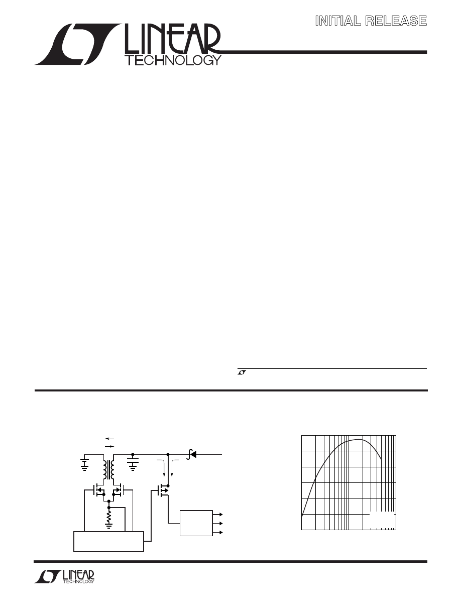
LTC1980
•
•
Li-Ion
BATTERY
POWER FLOW
CHARGING
BATTERY
OPERATION
SYSTEM
POWER
LDO/
SWITCH
3.3V
UNREGULATED
WALL ADAPTER
INPUT (3V TO 10V)
1.8V
1.5V
1980 TA01
SYSTEM LOAD
DC/DC
CONVERTERS
BAT-FET
REG-FET
Li-Ion Charger and DC/DC Converter Using One IC
LOAD CURRENT (mA)
10
EFFICIENCY (%)
90
85
80
75
70
65
60
100
1000
1980 G04
V
BAT
= 3.6V
T
A
= 25
°
C
FIGURE 5
3.3V Regulator Efficiency vs Load Current
LTC1980
2
1980i
ABSOLUTE AXI U RATI GS
W
W
W
U
PACKAGE/ORDER I FOR ATIO
U
U
W
V
REG
to GND ............................................. –0.5V to 12V
V
BAT
to GND ............................................. –0.5V to 12V
PROG, I
SENSE
.............................................. –0.5V to 5V
PROGT, REGFB, V
C
, BATT1, BATT2
TIMER, SS ............................................ –0.5V to V
BIAS2
LDOFB, LDODRV .................................... –0.5V to V
REG
WA, V
BIAS1
, REG ....................................... –0.5V to 12V
MODE ................................................... –0.5V to V
BIAS1
V
BIAS2
......................................................... –0.5V to 5V
OVP ............................................................ –0.5V to 5V
PGND to GND .................................... Connect Together
Operating Ambient Temperature Range
(Note 2) ................................................. – 40
°
C to 85
°
C
Storage Temperature Range ................. – 65
°
C to 125
°
C
Lead Temperature (Soldering, 10 sec)................ 300
°
C
(Note 1)
ORDER PART
NUMBER
1
2
3
4
5
6
7
8
9
10
11
12
TOP VIEW
GN PACKAGE
24-LEAD NARROW PLASTIC SSOP
24
23
22
21
20
19
18
17
16
15
14
13
SS
OVP
CAOUT
I
SENSE
GND
V
BIAS2
V
BAT
TIMER
MODE
REG
BGTDR
V
BIAS1
PROG
PROGT
REGFB
V
C
LDOFB
LDODRV
V
REG
WA
BATT1
BATT2
RGTDR
PGND
LTC1980EGN
T
JMAX
= 125
°
C,
θ
JA
= 85
°
C/W
Consult LTC Marketing for parts specified with wider operating temperature ranges.
ELECTRICAL CHARACTERISTICS
SYMBOL
PARAMETER
CONDITIONS
MIN
TYP
MAX
UNITS
V
BAT
Positive Supply Voltage, V
BAT
2.85
10
V
V
REG
Positive Supply Voltage, V
REG
2.85
10
V
V
FB
Feedback Voltage
REGFB Tied to V
C
●
1.194
1.225
1.256
V
V
PROGT
Voltage on PROGT Pin
PROGT Tied to V
C
1.194
1.225
1.256
V
I
BURST
Burst Mode Operation
Regulator Mode, REGFB = 1.5V
0.75
mA
Supply Current, Quiescent, V
REG
I
HIGH
Supply Current, Quiescent, V
REG
Regulator Mode, REGFB = 0V
●
2
4.3
mA
I
SHDN
Supply Current in Shutdown Mode, V
REG
Mode = 0V
15
µ
A
V
UVL
Positive-Going Undervoltage Lockout Voltage
From Either V
BAT
or V
REG
2.45
2.7
2.85
V
V
UVHYS
Undervoltage Lockout Hysteresis
From Either V
BAT
or V
REG
100
mV
I
SS
Soft-Start Ramp Current
BATT1 = 0, BATT2 = 0, Charger Mode
10
µ
A
V
FLOAT0
Output Float Voltage in Constant Voltage Mode
BATT1 = 0, BATT2 = 0
●
4.059
4.1
4.141
V
V
FLOAT1
Output Float Voltage in Constant Voltage Mode
BATT1 = 0, BATT2 = 0
●
4.158
4.2
4.242
V
V
FLOAT2
Output Float Voltage in Constant Voltage Mode
BATT1 = 0, BATT2 = 1 (Note 3)
●
8.118
8.2
8.282
V
V
FLOAT3
Output Float Voltage in Constant Voltage Mode
BATT1 = 0, BATT2 = 1 (Note 3)
●
8.316
8.4
8.484
V
V
FLOAT4
Output Float Voltage in Constant Voltage Mode
BATT1 = Open, BATT2 = Don’t Care
●
1.207
1.225
1.243
V
Measured from OVP Input
V
RCHG0
Recharge Threshold, Delta Voltage with Respect
BATT2 = 0, BATT1 = 0 or 1
200
mV
to Float Voltage
V
RCHG1
Recharge Threshold, Delta Voltage with Respect
BATT2 = 1, BATT1 = 0 or 1
400
mV
to Float Voltage
The
●
denotes the specifications which apply over the full operating
temperature range, otherwise specifications are at T
A
= 25
°
C. V
BAT
= 2.4V, V
REG
= 5V, V
BAT
unloaded.
LTC1980
3
1980i
ELECTRICAL CHARACTERISTICS
SYMBOL
PARAMETER
CONDITIONS
MIN
TYP
MAX
UNITS
V
RCHG2
Recharge Threshold, Delta Voltage with Respect
BATT 1 = Open
60
mV
to Float Voltage, Measured at OVP
V
LT0
Charger Shorted Cell Threshold
BATT2 = 0
2.55
2.7
2.8
V
V
LT1
Charger Shorted Cell Threshold
BATT2 = 1
5.2
5.4
5.65
V
I
BLDO
Input Bias Current, Low Dropout Regulator
Measured at LDOFB Pin
1.0
µ
A
g
mldo
Transconductance, Low Dropout Regulator
Measured from LDOFB to LDODRV
350
µ
mhos
V
OLLDO
Output Low Voltage, Low Dropout Regulator
0.1
V
V
OHLDO
Output High Voltage, Low Dropout Regulator
V
REG
– 0.1
V
I
OUTLDO
Low Dropout Regulator Output Current, Source/Sink
±
20
µ
A
A
VOL
Error Amplifier Open-Loop Voltage Gain
From REGFB to V
C
60
dB
I
BEA
Error Amplifier Input Bias Current
–0.1
0.1
µ
A
V
OLEA
Error Amplifier Output Low Voltage
0
0.5
V
V
OHEA
Error Amplifier Output High Voltage
SS = Open
1.4
2
V
I
OUT
Error Amplifier Output Source Current
0.5
mA
Error Amplifier Output Sink Current
–1.2
mA
g
mflt
Float Voltage Error Amplifier Transconductance
Measured from OVP to SS,
65
µ
mhos
Charger Mode, BATT1 = Open
I
BFLT
Float Voltage Error Amplifier Input Current
–0.1
0.1
µ
A
(Measured at OVP Input)
V
OS1
Current Amplifier Offset Voltage
–6
6
mV
I
BIS
Input Bias Current, I
SENSE
Input
–100
µ
A
A
VCA
Current Amplifier Voltage Gain
Measured from I
SENSE
to
2.3
2.44
2.55
V/V
CAOUT Pin
R
PROG
PROG Pin On Resistance
400
Ω
I
PROG
PROG Pin Leakage Current
100
nA
f
S
Switching Frequency
●
260
300
340
kHz
t
r
, t
f
Driver Output Transition Times
C
L
= 15pF
10
ns
t
BREAK
Driver Output Break Times
V
BAT
= V
REG
= 10V
100
ns
f
TIMER
Timer Frequency
C = 1000pF
4.5
kHz
I
TIMER1
TIMER Pin Source Current
–4
µ
A
I
TIMER2
TIMER Pin Sink Current
4
µ
A
R
REG
REG On Resistance
68
Ω
I
REGPD
REG Pull-Down Current
2
5
9
µ
A
I
REGLK
REG Leakage Current
60
nA
V
VTHREG
REG Logic Threshold
0.3
1.3
V
V
IL1
Digital Input Low Voltage,
V
REG
= 5V
1.185
1.221
1.247
V
Negative-Going, Wall Adapter (WA)
V
IH1
Digital Input High Voltage,
V
REG
= 5V
1.195
1.226
1.257
V
Positive-Going, Wall Adapter (WA)
V
IL2
Digital Input Low Voltage, BATT1
100
mV
V
IH2
Digital Input High Voltage, BATT1
V
BIAS2
–
V
100mV
The
●
denotes the specifications which apply over the full operating
temperature range, otherwise specifications are at T
A
= 25
°
C. V
BAT
= 2.4V, V
REG
= 5V, V
BAT
unloaded.
LTC1980
4
1980i
ELECTRICAL CHARACTERISTICS
The
●
denotes the specifications which apply over the full operating
temperature range, otherwise specifications are at T
A
= 25
°
C.V
BAT
= 2.4V, V
REG
= 5V, V
BAT
unloaded.
SYMBOL
PARAMETER
CONDITIONS
MIN
TYP
MAX
UNITS
V
P2
Digital Input Pull-Up Voltage, BATT1
BATT1 Input Floating
1.6
V
V
IL3
Digital Input Low Voltage, BATT2
0.3
V
V
IH3
Digital Input High Voltage, BATT2
2
V
I
I1
Digital Input Current, WA
–5
5
µ
A
I
I2
Digital Input Current, BATT1
–10
10
µ
A
I
I3
Digital Input Current, BATT2
–1
1
µ
A
Note 1: Absolute Maximum Ratings are those values beyond which the life
of a device may be impaired.
Note 2: The LTC1980E is guaranteed to meet performance specifications
from 0
°
C to 70
°
C. Specifications over the –40
°
C to 85
°
C operating
Feedback Reference Voltage
vs Temperature
Switching Frequency Variance
vs Temperature
Regulator Load Regulation
3.3V Regulator Efficiency
vs Load Current
5V Regulator Efficiency
vs Load Current
Regulator Load Step Response
TYPICAL PERFOR A CE CHARACTERISTICS
U
W
temperature range are assured by design, characterization and correlation
with statistical process controls.
Note 3: T
A
= 0
°
C to 70
°
C.
TEMPERATURE (
°
C)
FEEDBACK REFERENCE VOLTAGE (V)
1980 G01
1.2240
1.2235
1.2230
1.2225
1.2220
1.2215
1.2210
1.2205
–40
–15
10
35
60
85
TEMPERATURE (
°
C)
FREQUENCY VARIANCE (%)
1980 G02
1.5
1.0
0.5
0
–0.5
–1.0
–1.5
–40
–15
10
35
60
85
LOAD CURRENT (mA)
0
∆
V
REG
(%)
0
–0.2
–0.4
–0.6
–0.8
–1.0
–1.2
100
200
300
400
1980 G03
500
V
BAT
= 4.2V
V
REG
≅
3.3V
T
A
= 25
°
C
FIGURE 5
LOAD CURRENT (mA)
10
EFFICIENCY (%)
90
85
80
75
70
65
60
100
1000
1980 G04
V
BAT
= 3.6V
T
A
= 25
°
C
FIGURE 5
LOAD CURRENT (mA)
10
EFFICIENCY (%)
90
85
80
75
70
65
60
100
1000
1980 G05
V
BAT
= 3.6V
T
A
= 25
°
C
R8 = 309k
FIGURE 5
V
REG
50mV/DIV
100
µ
s/DIV
I
L
500mA/DIV
V
BAT
= 3.6V
V
REG
≅
3.3V
I
L
= 100mA TO 500mA
T
A
= 25
°
C
FIGURE 5
1980 G06
LTC1980
5
1980i
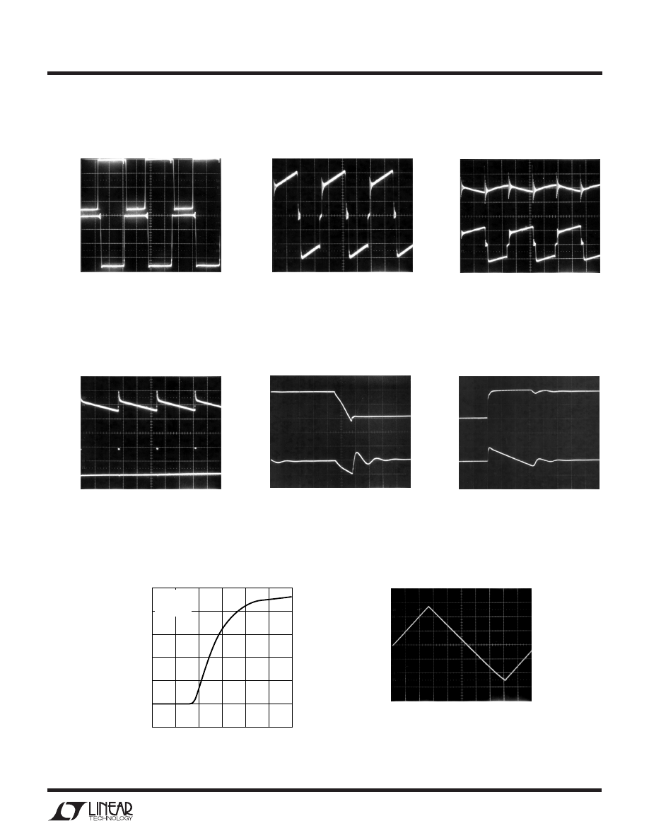
Typical BGTDR and RGTDR
Waveforms
Typical I
SENSE
Waveforms,
Regulator
Typical Operation with Burst
Mode Operation Disabled
TYPICAL PERFOR A CE CHARACTERISTICS
U
W
Burst Mode Circuit Operation
Regulator Output Transient
Response—Wall Adapter Removal
Mode Pin Input Current vs V
IN
Typical C
TIMER
Waveform
Regulator Output Transient
Response—Wall Adapter “Hot
Plugged”
BGTDR
1V/DIV
1
µ
s/DIV
RGTDR
1V/DIV
V
BAT
= 3.6V
V
REG
= 3.3V
T
A
= 25
°
C
I
L
= 500mA
1980 G07
I
SENSE
20mV/DIV
PIN 21
FIGURE 5
1
µ
s/DIV
V
BAT
= 3.6V
V
REG
= 3.3V
I
L
= 500mA
T
A
= 25
°
C
FIGURE 5
1980 G08
V
REG
50mV/DIV
1
µ
s/DIV
I
SENSE
50mV/DIV
V
BAT
= 3.6V
V
REG
≅
3.3V
I
L
= 500mA
MODE = V
BIAS1
T
A
= 25
°
C
FIGURE 5
1980 G09
V
REG
50mV/DIV
200
µ
s/DIV
BGTDR
2V/DIV
V
BAT
= 3.6V
V
REG
= 3.3V
I
L
= 10mA
T
A
= 25
°
C
FIGURE 5
1980 G10
MODE PIN V
IN
(V)
0
MODE PIN INPUT CURRENT (
µ
A)
1.5
1.0
0.5
0
–0.5
–1.0
–1.5
0.5
1.0
1.5
2.0
1980 G13
2.5
3.0
V
BAT
= 2.4V
V
REG
= 5V
T
A
= 25
°
C
V
REG
1V/DIV
500
µ
s/DIV
V
LDO
0.1V/DIV
V
BAT
= 3.6V
V
REG
= 3.3V
V
LDO
= 3.1V
I
LDO
= 200mA
V
WALL ADAPTER
= 6V TO 0V
T
A
= 25
°
C
FIGURE 5
1980 G11
V
REG
1V/DIV
500
µ
s/DIV
V
LDO
0.5V/DIV
V
BAT
= 3.6V
V
REG
= 3.3V
V
LDO
= 3.1V
I
LDO
= 200mA
V
WALL ADAPTER
= 0V TO 6V
T
A
= 25
°
C
FIGURE 5
1980 G12
TIMER
100mV/DIV
PIN 17
5ms/DIV
C
TIMER
= 0.24
µ
F
T
A
= 25
°
C
1980 G14
LTC1980
6
1980i
U
U
U
PI FU CTIO S
PROG (Pin 1): Charge Current Ratio Programming Pin.
Programs the full charge current when the charger is in the
constant current mode. A resistor placed between the
PROG pin and the PROGT pin (Pin 2) determines the
charge current. The PROG pin connects to an open drain
MOSFET which turns on for full current and is off when
trickle charging.
PROGT (Pin 2): Trickle Charge Programming Pin. Pro-
grams the trickle charge current for a deeply discharged
battery. Two resistors are used, one between the PROGT
pin and CA
OUT
(Pin 22) and another from PROGT to
ground. A capacitor between the PROGT pin and V
C
(Pin
4) provides compensation for the constant current feed-
back loop.
REGFB (Pin 3): DC/DC Converter Feedback Pin. This pin is
used to program the DC/DC converter output voltage when
the LTC1980 is in the DC/DC (regulator) converter mode.
An external resistor divider from V
REG
to REGFB to ground
programs the output voltage. The virtual reference voltage
(V
REF
) on this pin is 1.225V. A series RC from the REGFB
pin to V
C
(Pin 4) provides pole-zero compensation for the
regulator outer loop.
V
C
(Pin 4): Control Signal of the Inner Loop of the Current
Mode PWM. A common current mode loop is used by the
battery charger and voltage regulator functions. Minimum
duty factor (measured on BGTDR (Pin 14) in regulator
mode and RGTDR (Pin 11) in charger mode) occurs at
approximately 1V. Duty factor increases as V
C
increases.
This part includes slope compensation, so there is some
variation in V
C
for minimum and maximum duty factor as
V
REG
or V
BAT
is varied.
LDOFB (Pin 5): Low Dropout Regulator Feedback Pin.
This pin is used to program the low dropout linear regula-
tor output voltage. An external resistor divider from the
output of the LDO regulator (drain of the external MOSFET)
to LDOFB to ground programs the output voltage. The
virtual reference voltage on this pin is 1.225V.
LDODRV (Pin 6): Low Dropout Error Amplifier Output.
This pin drives the gate of an external PMOS pass transis-
tor. This pin is pulled up to V
REG
(shutting off the pass
transistor) if MODE (Pin 16) is grounded or if undervoltage
occurs.
V
REG
(Pin 7): Connection Point to the DC/DC Converter
Side of the Combo Charger/Converter Circuit.
WA (Pin 8): Wall Adapter Comparator Input. An external
resistor divider from the wall adapter output to WA to
ground sets the threshold which determines if charging
can occur. If the wall adapter is below this threshold, the
LTC1980 assumes the wall adapter is not present and the
charger shuts down. Wall adapter sense threshold is set
higher than the DC/DC converter output voltage to insure
correct operation.
BATT1 (Pin 9): Logic Input Pin for Selecting
Preprogrammed Li-Ion Charge Voltage. See Truth Table
logic settings.
BATT2 (Pin 10): Logic Input Pin for Selecting
Preprogrammed Li-Ion Charge Voltage. The following
combinations of BATT1 and BATT2 select the correct Li-
Ion charge voltage. See Truth Table.
BATT2
BATT1
FLOAT VOLTAGE
0
0
4.1V
0
1
4.2V
1
0
8.2V
1
1
8.4V
Don’t Care
Open
Externally Set Via OVP
Logic 1 = V
BIAS2
(Pin 19), Logic 0 = GND
RGTDR (Pin 11): DC/DC Converter (Regulator) Side Gate
Drive Pin. This pin provides gate drive to the external
MOSFET (REG-FET) that connects to V
REG
via the trans-
former.
PGND (Pin 12): Power Ground. Refer to the Applications
Information section for proper use of ground and power
ground connections.
V
BIAS1
(Pin 13): Internally Generated Power Bus. Bypass
this pin with a 1
µ
F or larger ceramic capacitor (or other low
ESR capacitor) to PGND (Pin 12). Do not connect any load
to this pin.
BGTDR (Pin 14): DC/DC Converter (Battery) Side Gate
Drive Pin. This pin provides gate drive to the external
MOSFET (BAT-FET) that connects to V
BAT
via the trans-
former.

LTC1980
7
1980i
REG (Pin 15): Bidirectional Regulator Mode Control Pin.
A
pull-up resistor is required between this pin and V
BIAS2
.
This pin is open when charging normally, has a weak pull-
down (approximately 5
µ
A) when conditioning the battery
and a strong pull-down when in regulator mode. Pulling
this pin low forces the IC into regulator mode.
MODE (Pin 16): Selects different operating modes in both
charger and DC/DC converter configurations. Also en-
ables and disables Burst Mode operation. See Mode Pin
Operation table in Application section.
TIMER (Pin 17): A timing capacitor on this pin determines
the normal charge time for charge termination.
C(
µ
F) = 0.25 • Time (Hours)
V
BAT
(Pin 18): This pin connects to the positive terminal of
the battery and the battery side of the power converter.
V
BIAS2
(Pin 19): Internally Generated Voltage. Bypass this
pin with a 1
µ
F or larger ceramic capacitor (or other low
ESR capacitor). Do not connect any load to this pin.
GND (Pin 20): Signal Ground. This pin should Kelvin-
connect to the current sense resistor (R
SENSE
).
I
SENSE
(Pin 21): Current Sense Input Pin. Connects inter-
nally to a current amplifier and zero current comparator.
This pin should Kelvin-connect to the current sense resis-
tor (R
SENSE
) .
CAOUT (Pin 22): Current Amplifier Output. A program
resistor connects between this pin and PROGT (Pin 2) to
set the charge current (in constant-current mode).
OVP (Pin 23): Overvoltage Protection. This pin connects
to the tap on an optional external voltage divider con-
nected across the battery. This allows nonstandard float
voltages to be used for the battery charger. Overvoltage,
restart and undervoltage thresholds will also be affected
by the external voltage division ratio. To use this pin,
BATT1 (Pin 9) must float.
SS (Pin 24): Soft-Start. A capacitor between this pin and
ground sets the battery charge ramp rate. Battery charge
current is very low the moment after the converter switches
from DC/DC converter (regulator) mode to battery charger
mode then ramps up to final battery charge current from
there. This insures that the wall adapter is not loaded down
with a large inrush current that could prevent correct
battery charger operation.
The same capacitor, which sets the soft-start ramp rate,
also sets the compensation for the battery float voltage
control loop.
U
U
U
PI FU CTIO S
LTC1980
8
1980i
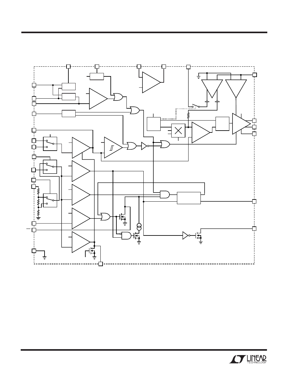
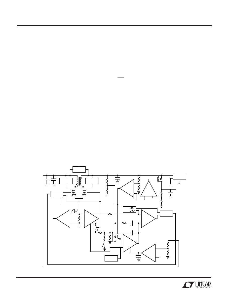
BLOCK DIAGRA
W
–
+
–
+
–
+
–
+
–
+
–
+
–
+
V
MAX
V
DD
REG
MODE
REFERENCE
18
9
13
6
21
22
7
19
16
2
3
4
15
8
20
24
11
14
12
17
1
V
REF
V
REF
–
+
–
+
V
REF
V
REF
V
REF
V
REF
AC
V
REF
V
REF
V
REF
START
SHORT CYCLE
TIMEOUT
TIMER
23
18
10
9
H = BURST MODE OPERATION OFF
OPEN = BURST MODE OPERATION ON
L = DISABLE
L
H
–
+
+
–
+
–
+
–
V
REF
V
REG
V
BAT
V
REF
V
REF
CAOUT
DUMP
XFMR
RAMP
OSC
S
Q
R
AC
V
M
REG
V
BAT
BURST
WAKE
SLEEP
DIS
UVL
REF_UVL
BATT1
V
BAT
V
REG
V
C
MODE
V
BIAS2
5
µ
A
SS
REG
WA
GND
GM
V
CELL
<3.8V
CONDITION BATTERY
EA
TIMER
PROG
1980 BD
PWM
COMP
LDOFB
LDODRV
SR_EN
I = O
COMP
I
SENSE
PGND
RGTDR
BGTDR
PROGT
REGFB
V
BIAS1
GM
BATT2
BATT1
OVP
5
LTC1980
9
1980i
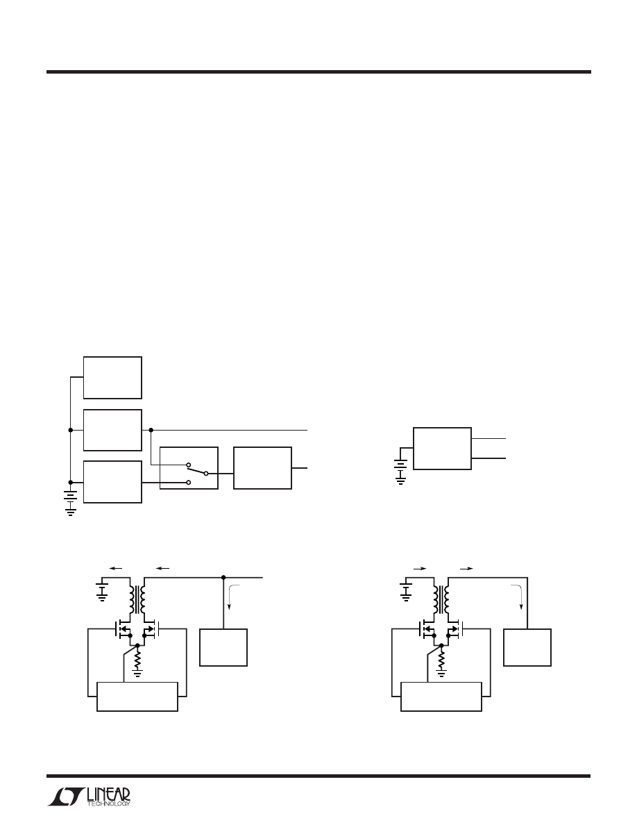
The LTC1980 is an IC designed to provide a regulated
voltage to a system load from an unregulated or regulated
wall adapter, or from a battery and also charge a battery,
thereby providing an uninterruptable power source for the
system. When the wall adapter is present it provides
power to the system load and, if needed, a portion of the
power can be used to simultaneously charge the battery.
If the wall adapter is removed, the LTC1980 uses the
battery as a power source to continue providing a regu-
lated output voltage to power the system.
Combining these two functions into a single IC reduces
circuit area compared to presently available solutions
OPERATIO
U
(Figure 1). The unique bidirectional power converter to-
pology (Figure 2) accounts for much of the area savings.
A transformer based design allows the wall adapter volt-
age to be less than or greater than the battery voltage.
The LTC1980 includes a 300kHz DC/DC PWM converter
that operates in two modes. The first mode is when the wall
adapter is present and the LTC1980 is used to charge the
battery using a constant-current/constant-voltage charge
scheme. The second mode is when the wall adapter is
removed and the battery powers the LTC1980 and the
DC/DC converter generates a regulated output voltage.
POWER ROUTING
Existing Methods
Using the LTC1980
LOW DROPOUT
REGULATOR
TO SYSTEM LOAD
DC/DC CONVERTERS
TO SYSTEM LOAD
DC/DC CONVERTERS
FROM WALL ADAPTER
1980 F01
FROM
WALL ADAPTER
PWM
REGULATOR
BATTERY
CHARGER
CHARGE
TERMINATION
LTC1980-BASED
POWER DESIGN
Figure 1. Portable Power Systems
LTC1980
I
SENSE
•
•
Li-Ion
BATTERY
T1
WALL
ADAPTER
1980 F02a
SYSTEM LOAD
DC/DC
CONVERTERS
BAT-FET
REG-FET
R
S
Figure 2. LTC1980 Bidirectional Power Conversion
(a) Battery Charger Mode
LTC1980
I
SENSE
•
•
Li-Ion
BATTERY
T1
1980 F02a
SYSTEM LOAD
DC/DC
CONVERTERS
BAT-FET
REG-FET
R
S
(b) DC/DC Converter Mode (Wall Adapter Removed)
LTC1980
10
1980i
Lithium-Ion Battery Charger Operation
With the wall adapter power applied, the LTC1980 oper-
ates as a constant-current/constant-voltage PWM battery
charger, with a portion of the adapter current used for
charging and the rest flowing to the system load through
an optional low dropout regulator.
A charge cycle begins when the voltage at V
REG
exceeds
the undervoltage lockout threshold level and the IC is
enabled via the MODE pin. If the battery has been deeply
discharged and the battery voltage is less than 2.7V, the
charger will begin with the programmed trickle charge
current.
When the battery exceeds 2.7V, the charger begins the
constant-current portion of the charge cycle with the
charge current equal to the programmed level. As the
battery accepts charge, the voltage increases. When the
battery voltage reaches 3.8V, the programmable timer
begins. Constant-current charging continues until the
battery approaches the programmed charge voltage of
4.1V or 4.2V/cell at which time the charge current will
begin to drop, signaling the beginning of the constant-
voltage portion of the charge cycle. The charger will
maintain the programmed preset float voltage across the
battery until the timer terminates the charge cycle. During
trickle charging, if the battery voltage remains below 2.7V
for 1/4 of the total programmed charge time, the battery
may be defective and the charge cycle ends. Also, if a
battery open circuit is detected, the charge cycle ends
immediately. The charger can be shut down by pulling the
REG pin low, although the timer will continue until it times
out.
Power Converter Operation from Battery
When the AC adapter is removed, the LTC1980 operates as
a DC/DC PWM converter using the battery for input power
to provide a regulated output voltage for the system load.
The LTC1980 is a current mode switcher. This means that
the switch duty cycle is directly controlled by switch
current rather than by output voltage or current. Battery
charger operation will be described for the simplified
diagram (Figure 3). At the start of the oscillator cycle, latch
U9 is set causing M2 to turn on. When switch current
reaches a predetermined level M2 turns off and M1 turns
on. This level is set by the control voltage at the output of
error amplifier U10.
OPERATIO
U
U4
DRIVERS
BDRIVE
–
+
–
+
–
+
–
+
–
+
–
+
–
+
T1
U1 VOLTAGE
SELECTION
B1
C1
+
RDRIVE
U11
REFERENCE
R1
R7
R2
R5
C2
R12
TO SYSTEM
LOAD
R13
R8
R9
U2
V
REF
V
REF
U5
U6
U8
U10
DIRECTION
TYPICAL
WAVEFORM
CURRENT
AMPLIFIER
SENSE
ZC
SW1
SW3
SW2
EA
C5
U7
OSC
R6
C3
C4
PWM
WALL
ADAPTER
S
R
Q
U9
1980 F03
M1 M2
R4
SN1 SNUBBER
NETWORK
SN2 SNUBBER
NETWORK
–
+
U12
V
REF
R10
R11
C6
V
BAT
V
REG
Figure 3. Simplified Diagram—Power Converter
LTC1980
11
1980i
Transformer current is sensed across R
S
, gained up via U6
and sampled through switch SW1. The current in R7 is a
scaled-down replica of the battery charging current pulses
from the transformer. During battery charging, switch
SW2 is in the down position connecting R7, R8, R9 and C4
to the inverting input of amplifier U10 forming an integra-
tor which closes the outer loop of the converter and
establishes constant current charging. U12 is a g
m
ampli-
fier that clamps U10 as the battery float voltage is reached.
R10 and R11 set the float voltage and C5 compensates this
loop and provides a soft-start function.
OPERATIO
U
DC/DC Converter Operation
When the LTC1980 is operating as a DC/DC converter, M1
turns on at the start of the oscillator cycle. When trans-
former current reaches a predetermined level set by U10’s
output voltage, M1 turns off and M2 turns on. SW2 is in the
up position forming an integrator with zero, which com-
pares the output voltage (via R1 and R2 to reference U11
establishing the output voltage.
APPLICATIO S I FOR ATIO
W
U
U
U
Setting Battery Charge Current
Referring to the simplified schematic in Figure 4, the
average current through R7 must equal the current through
R
TRKL
with switch SW3 open. This leads to the equation
for setting the trickle charge current:
R
V
R
I
R
A
TRKL
REF
TRICKLE
S
V
=
•
•
•
7
Normal charge current is set via the parallel combination
of R
TRKL
and R
CHRG
which leads to the following equation
for R
CHRG
R
V
R
I
I
R
A
CHRG
REF
NORMAL
TRICKLE
S
V
=
(
)
•
–
•
•
7
–
+
21
U6
A
V
= 2.5
–
+
U10
R
S
I
SENSE
22
20
CAOUT
2
1
PROGT
V
REF
1.218V
22
V
C
C4
R7
10k
R
TRKL
SW1
20
GND
I
R
CHRG
PROG
SW3
1980 F04
Figure 4. Battery Charger Current Control Loop
where A
V
= 2.44 and V
REF
= 1.225V. The suggested value
for R7 is 10k.
Setting the Float Voltage
Pin selectable 4.1V, 4.2V, 8.2V, and 8.4V Li-Ion float
voltages are available. Other float voltages may be set via
external resistors. The following combinations of logic
inputs BATT1 and BATT2 determine the float voltage.
BATT2
BATT1
FLOAT VOLTAGE
0
0
4.1V
0
1
4.2V
1
0
8.2V
1
1
8.4V
Don’t Care
Open
Externally Set via OVP
where logic 0 = GND and logic 1 = V
BIAS2
(Pin 19)
LTC1980
12
1980i
APPLICATIO S I FOR ATIO
W
U
U
U
An external resistor divider (Figure 3) can be used to
program other float voltages. Resistor values are found
using the following equation:
R10 = R11 • (V
FLOAT
– V
REF
)/V
REF
where V
REF
= 1.225V. The suggested value for R11 is
100k. Use 1% or better resistors.
Setting DC/DC Converter Output Voltage
From Figure 5, select the following resistors based on
output voltage V
REG
:
R8 = R14 • (V
REG
– V
REF
)/V
REF
where V
REF
= 1.225V, suggested value for R14 is 100k, 1%.
LDO Operation
The LTC1980 provides an uninterrupted power supply for
the system load. When a wall adapter is connected and
operating, power is taken from the wall adapter to charge
the batteries and supply power to the system. In applica-
tions where an unregulated wall adapter is used but a
regulated voltage is needed by the system, an external P-
channel MOSFET pass transistor may be added to the
LTC1980 to create a low dropout linear regulator.
From Figure 5, select the following resistors based on the
output voltage V
LDO
:
R5 = R6 • (V
LDO
– V
REF
)/V
REF
where V
REF
= 1.225V, suggested value for R6 is 100k, 1%.
This is the voltage that will be seen when operating from
a higher voltage wall adapter. When operating from the
batteries (as a regulator), the load will see either this
voltage or the voltage set by the PWM regulator, which-
ever is less, minus any drops in the pass transistor.
Placing a large-valued capacitor from the drain of this
MOSFET to ground creates output compensation.
Wall Adapter Comparator Threshold
From Figure 5, select the following resistors based on the
wall adapter comparator threshold V
WATH
:
R15 = R7(V
WATH
– V
IH1
)/V
IH1
where V
IH1
= 1.222V, suggested value for R7 is 100k. Use
1% resistors.
MODE Pin Operation
The following truth table describes MODE pin operation.
Burst Mode operation is disabled during battery charging
to reduce broadband noise inherent in Burst Mode opera-
tion. (Refer to the LT1307 data sheet for details).
POWER FLOW
MODE PIN
OPERATING MODE
Battery Charger
0
Disabled
Battery Charger
Open
Enabled Continuous
Battery Charger
1
Enabled Continuous
DC/DC converter
0
Disabled
DC/DC converter
Open
Enabled Burst Mode Operation
DC/DC converter
1
Enabled Continuous
Logic 1 = V
BIAS1
(Pin 13) Logic 0 = GND
The MODE pin should be decoupled with 200pF to ground
when left open.
Snubber Design
The values given in the applications schematics have been
found to work quite well for most applications. Care
should be taken in selecting other values for your applica-
tion since efficiency may be impacted by a poor choice. For
a detailed look at snubber design, several very helpful
notes are available in Application Note 19.
Frequency Compensation
Load step testing can be used to empirically determine
compensation. Application Note 25 provides information
on the technique. To adjust the compensation for the DC/
DC converter, adjust C12 and R13 (in Figure 5). Battery
charger current loop compensation is set by C11 and
battery charger float voltage compensation is set by C8.
Component Selection Basics
The application circuits work well for most 1- and 2-cell
Li-Ion, 0.5A to 1A output current designs. The next section
highlights the component selection process. More infor-
mation is available in Application Note 19.
LTC1980
13
1980i
the transformer which can reduce the leakage inductance,
reduce the need for aggressive snubber design and for this
reason improve efficiency.
Avoid transformer saturation under all operating condi-
tions and combinations (usually the biggest problems
occur at high output currents and extreme duty cycles.
Also
check these conditions for battery charging and
regulation modes.
Finally, in low voltage applications, select a transformer
with low winding resistance. This will improve efficiency at
heavier loads.
Capacitors
Check the RMS current rating on your capacitors on both
sides of your circuit. Low ESR and ESL is recommended
for lowest ripple. OS-CON capacitors (from Sanyo) work
very well in this application.
Diodes
In low voltage applications, Schottky diodes should be
placed in parallel with the drain and source of the MOSFETs
in the PWM supply. This prevents body diode turn on and
improves efficiency by eliminating loss from reverse re-
covery in these diodes. It also reduces conduction loss
during the RGTDR/BGTDR break interval.
The LTC1980 can operate to voltages as low as 2.8V.
Suitable Schottky diodes include the ZHCS1000 (V
F
=
420mV at I
F
= 1A) and SL22/23 (V
F
= 440mV at I
F
= 2A) for
most 500mA to 1A output current applications.
Vendor List
VENDOR
COMPONENTS
TELEPHONE
BH Electronics
Transformers
952-894-9590
Coiltronics/Cooper Electronic
Transformers
561-241-7876
Fairchild Semiconductor
MOSFETs
Schottky Rectifiers
800-341-0392
Vishay (General Semiconductor) MOSFETs
Schottky Rectifiers
631-847-3000
Sanyo
OS-CON Capacitors
408-749-9714
Sumida Electric USA
Transformers
847-956-0666
Vishay (Siliconix)
MOSFETs
408-988-8000
APPLICATIO S I FOR ATIO
W
U
U
U
Current Sense Resistor
Voltage drop in the current sense resistor should be
limited to approximately
±
100mV with respect to ground
at max load currents in all modes. This value strikes a
reasonable balance between providing an adequate low
current signal, while keeping the losses from this resistor
low. For applications where the inputs and output voltages
may be low, a somewhat lower drop can be used (in order
to reduce conduction losses slightly).
The LTC1980 has several features, such as leading-edge
blanking, which make application of this part easier to use.
However for best charge current accuracy, the current
sense resistor should be Kelvin sensed.
MOSFETs
The LTC1980 uses low side MOSFET switches. There are
two very important advantages. First, N-channel MOSFETs
are used—this generally means that efficiency will be
higher than a comparable on-resistance P-channel device
(because less gate charge is required). Second, low V
T
(‘logic-level’) MOSFETs with relatively low absolute maxi-
mum V
GS
ratings can be used, even in higher voltage
applications. Refer to Application Note 19 for information
on determining MOSFET voltage and current ratings.
Transformer
Turns ratio affects the duty factor of the power converter
which impacts current and voltage stress on the power
MOSFETs, input and output capacitor RMS currents and
transformer utilization (size vs power). Using a 50% duty
factor under nominal operating conditions usually gives
reasonable results. For a 50% duty factor, the turns ratio
is:
N = V
REG
/V
BAT
N should be calculated for the design operating as a DC/DC
converter and as a battery charger. The final turns ratio
should be chosen so that it is approximately equal to the
average of the two calculated values for N. In addition
choose a turns ratio which can be made from the ratio of
small integers. This allows bifilar windings to be used in
LTC1980
14
1980i
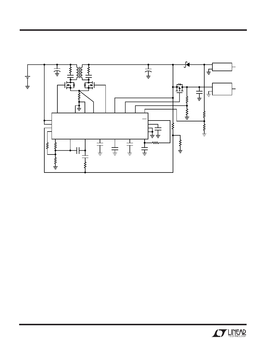
TYPICAL APPLICATIO
U
16
1980 TA02
REG
MODE
BATT1
BATT2
V
BAT
OVP
REGFB
CAOUT
C10
0.33
µ
F
PROG
C9
1
µ
F
C8
0.1
µ
F
C7
0.27
µ
F
R12
100k
R11
1M
R13
806k
PROGT
V
C
TIMER
SS
V
BIAS1
V
BIAS2
BGTDR
PGND
I
SENSE
RGTDR
LTC1980
GND
1/2 FDC6401N
1/2 FDC6401N
C6
470
µ
F
R5
154k
R6
100k
R7
100k
R14
100k
R8
169k
OPTIONAL PASS
TRANSISTOR
FOR LDO FDC636P
WALL
ADAPTER
SYSTEM LOAD
DC/DC
CONVERTERS
R9
10k
R10
110k
C11
1nF
C12
82pF
C1
68
µ
F
+
4.1V
Li-Ion
BATTERY
C4
68
µ
F
D1*
5819
50m
Ω
R
SENSE
+
+
V
REG
LDODRV LDOFB
WA
•
•
V
BAT
V
REG
DC
OUT
V
OUT
AC
IN
5.1
Ω
5.1
Ω
1nF
1nF
*OPTIONAL DIODE FOR
SHORTED WALL ADAPTER
TERMINAL PROTECTION.
R15
300k
18
15
9
10
14
1
2
4
17
24
13
19
12
20
21
11
7
6
5
8
23
3
22
BH511-1014
3.3V
200pF
V
LDO
3.1V
Figure 5. 4.1V/1A Li-Ion Battery Charger and 3.3V DC/DC Converter
LTC1980
15
1980i
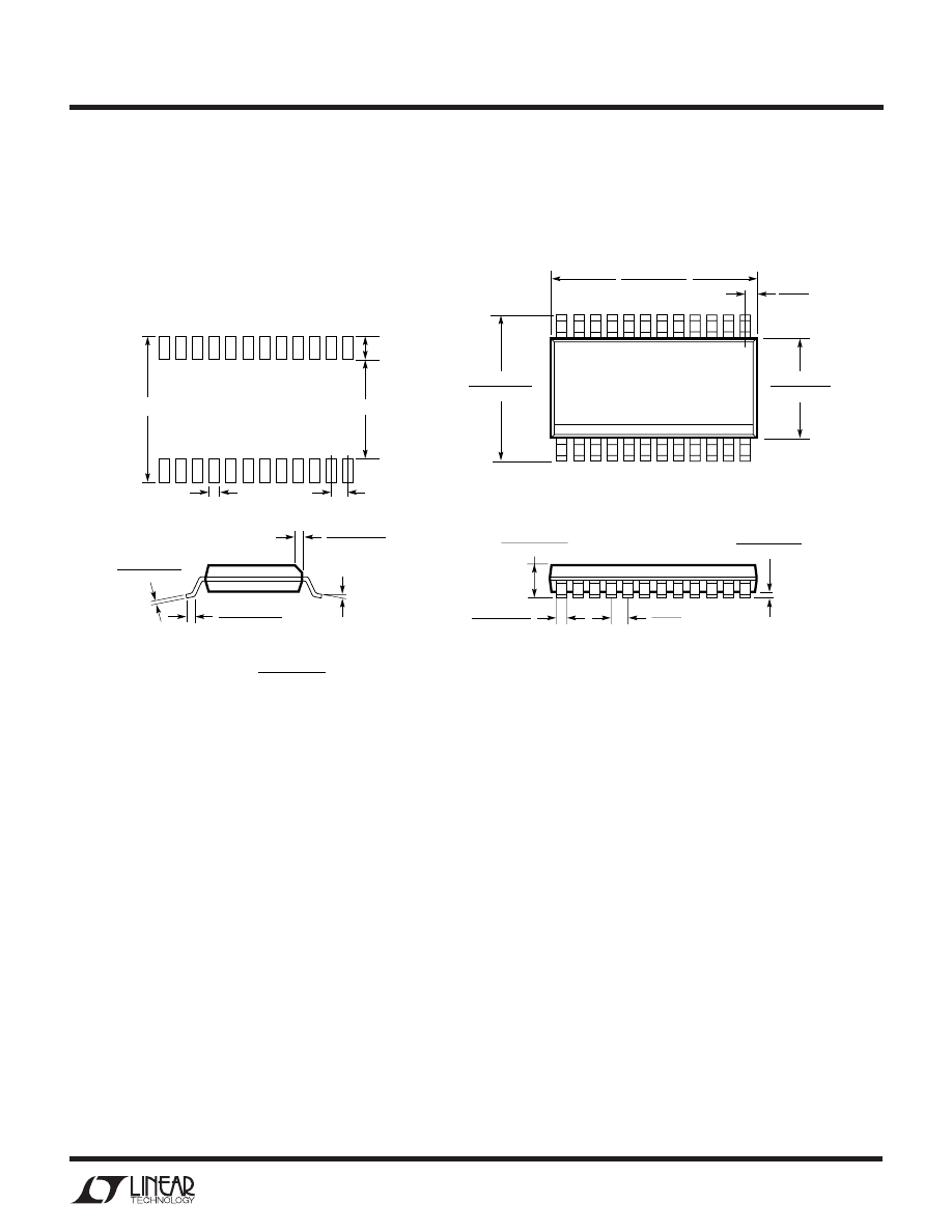
PACKAGE DESCRIPTIO
U
GN Package
24-Lead Plastic SSOP (Narrow .150 Inch)
(Reference LTC DWG # 05-08-1641)
.337 – .344*
(8.560 – 8.738)
GN24 (SSOP) 0502
1
2
3
4
5
6
7
8
9 10 11 12
.229 – .244
(5.817 – 6.198)
.150 – .157**
(3.810 – 3.988)
16
17
18
19
20
21
22
23
24
15 1413
.016 – .050
(0.406 – 1.270)
.015
±
.004
(0.38
±
0.10)
×
45
°
0
°
– 8
°
TYP
.007 – .0098
(0.178 – 0.249)
.053 – .068
(1.351 – 1.727)
.008 – .012
(0.203 – 0.305)
.004 – .0098
(0.102 – 0.249)
.0250
(0.635)
BSC
.033
(0.838)
REF
.254 MIN
RECOMMENDED SOLDER PAD LAYOUT
.150 – .165
.0250 TYP
.0165
±
.0015
.045
±
.005
*DIMENSION DOES NOT INCLUDE MOLD FLASH. MOLD FLASH
SHALL NOT EXCEED 0.006" (0.152mm) PER SIDE
**DIMENSION DOES NOT INCLUDE INTERLEAD FLASH. INTERLEAD
FLASH SHALL NOT EXCEED 0.010" (0.254mm) PER SIDE
INCHES
(MILLIMETERS)
NOTE:
1. CONTROLLING DIMENSION: INCHES
2. DIMENSIONS ARE IN
3. DRAWING NOT TO SCALE
LTC1980
16
1980i
Linear Technology Corporation
1630 McCarthy Blvd., Milpitas, CA 95035-7417
(408) 432-1900
●
FAX: (408) 434-0507
●
www.linear.com
LINEAR TECHNOLOGY CORPORATION 2003
LT/TP 0403 1.5K • PRINTED IN USA
RELATED PARTS
PART NUMBER
DESCRIPTION
COMMENTS
LT1170/LT1171/LT1172 5A/3A/1.25A Flyback Regulators
Isolated Flyback Mode
LT1571
200kHz/500kHz Switching Battery Charger
Up to 1.5A Charge Current; Preset and Adjustable Battery Voltages
LTC1729
Lithium-Ion Battery Charger Termination Controllers Time or Charge Current Termination, Preconditioning 8-Lead MSOP
LTC1730
Lithium-Ion Battery Pulse Charger
No Blocking Diode Required, Current Limit for Maximum Safety
LTC1731
Lithium-Ion Linear Battery Charger Controller
Simple Charger uses External FET, Features Preset Voltages, C/10
Charger Detection and Programmable Timer
LTC1732
Lithium-Ion Linear Battery Charger Controller
Simple Charger uses External FET, Features Preset Voltages, C/10
Charger Detection and Programmable Timer, Input Power Good Indication
LTC1733
Monolithic Lithium-Ion Linear Battery Charger
Standalone Charger with Programmable Timer, Up to 1.5A Charge Current
LTC1734
Lithium-Ion Linear Battery Charger in ThinSOT
TM
Simple ThinSOT Charger, No Blocking Diode, No Sense Resistor Needed
LTC1734L
Lithium-Ion Linear Battery Charger Controller
50mA to 180mA, No Blocking Diode, No Sense Resistor Needed
LTC1960
Dual Battery Charger/Selector with SPI
Complete Dual-Battery Charger/Selector System, Easy Interface with
Microcontroller, Extends Run Time by 10%, reduces Charge Time by 50%
LTC4007
4A Standalone Multiple Cell Li-Ion Battery Charger
6V
≤
V
IN
≤
28V, 3- or 4-Cell, Up to 96% Efficiency
LTC4050
Lithium-Ion Linear Battery Charger Controller
Simple Charger uses External FET, Thermistor Input for
Battery Temperature Sensing
LTC4052
Lithium-Ion Linear Battery Pulse Charger
Fully Integrated, Standalone Pulse Charger, Minimal Heat Dissipation,
Overcurrent Protection
LTC4412
Ideal Diode or PowerPath
TM
Very Low Loss Replacement for Power Supply, ORing Diodes,
3V
≤
V
IN
≤
28V, ThinSOT
Package.
ThinSOT and PowerPath are trademarks of Linear Technology Corporation.
Wyszukiwarka
Podobne podstrony:
AVR450 Battery Charger for SLA NiCd NiMH and Li ion Batterie
AVR Battery Charger for SLA, NiCd, NiMH and Li Ion Batteries
9 CD 4212 2 battery charger
DIY Combination Solar Water and Nieznany
Direct Conversion Receiver, MPSKIQ and Direct Conversion
Ouellette J Science and Art Converge in Concert Hall Acoustics
Batteries & Charge Control in Stand Alone PV Systems
Bedini Radiant Battery Charger (Free Energy)
Battery Charger Voltage Settings
BATTERY CHARGER SPARE PARTS
charged and rotating ADS black holes and their CFT duals
20 Years Bearden Bedini Free Energy Generation Solid State Battery Charger
9 CD 4212 2 battery charger
DIY Combination Solar Water and Nieznany
Synchronous Generator And Frequency Converter In Wind Turbine Applications System Design And Efficie
9 CD 4212 2 battery charger
Metric and imperial conversions
Instrukcja obsługi prostownika Car Battery Charger ULG 3,8 A1
więcej podobnych podstron