Operational Description
Functional Description
Hawaii Refresh cellular phone operates in GSM, DCS, and CEL & PCS bands. It
provides GPRS class 10, EDGE class 10 and Bluetooth class 2 data support. It
consists of RFMD Prime chipsets, Neptune LTE2, Atlas Ultra-Lite, Bluetooth
module, internal system memory of 512Mbit flash, 128Mbit PSRAM and
removable memory storage in the form of microSD memory card up to 2GB. It
also embedded a 2MP CMOS camera, FM radio and MegaSIM capabilities.
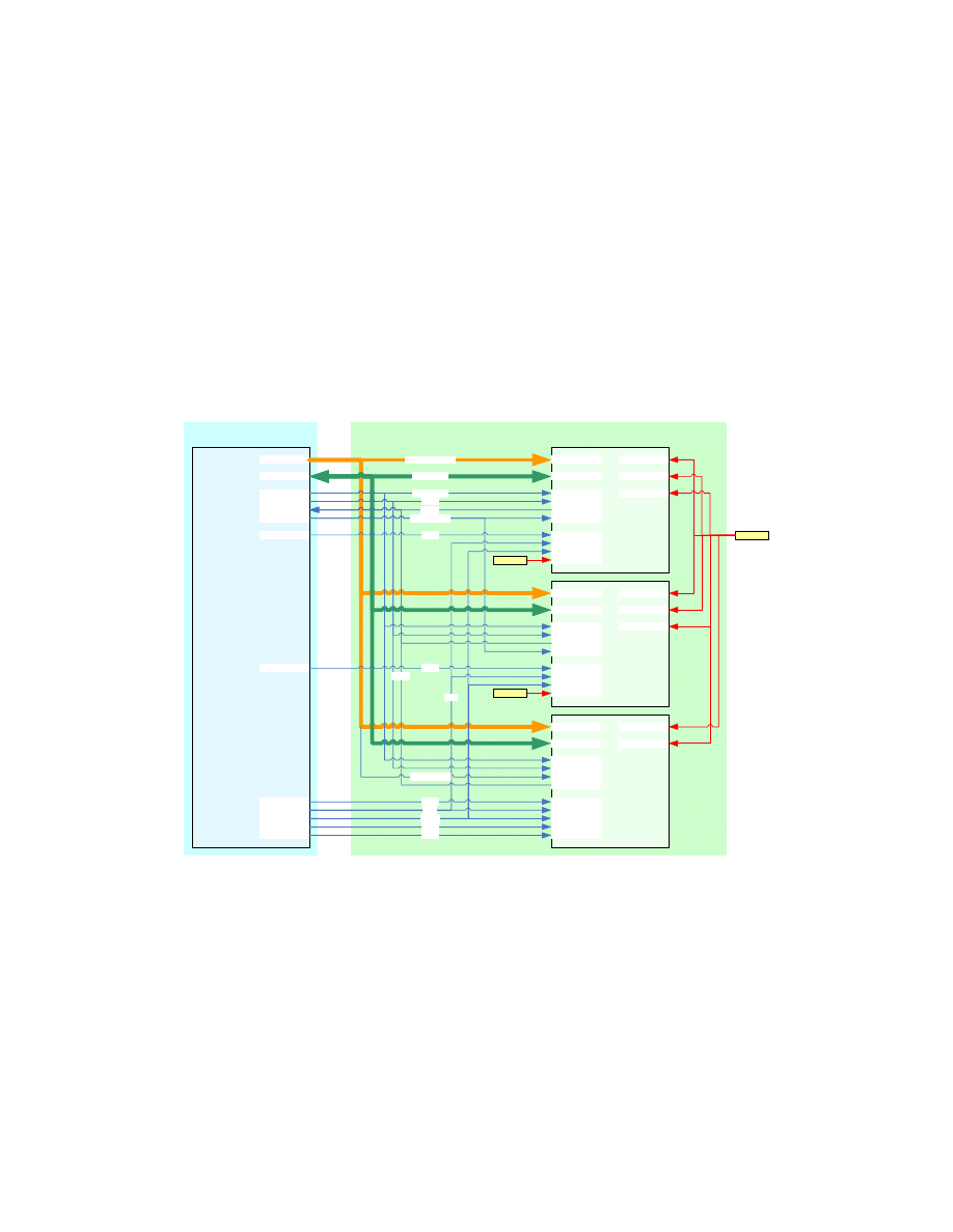
Hardware Interface
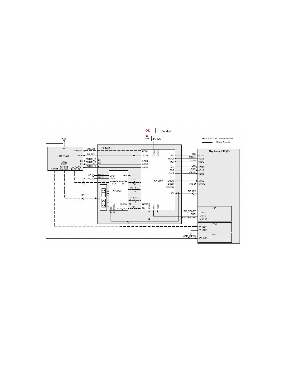
The signaling diagram shows a general view of the interfaces involved between
the chips on the RF portion of the radio. RF6027 and RF3178 formed the RFMD
Prime chipset.
Antenna Switch
An internal antenna switch is employed in this design. The antenna switch
routes the appropriate band transmit or receive signal between the antenna and
respective IC. It is controlled by 3 control lines, B1, B2 and B3, coming from the
RF6027.

RF3178
The RF3178 module is a 50
Ω
input/output, quad-band, dual-mode,
GMSK/8PSK(EDGE) PA module intended for 2.75G radio applications. The
module consists of a dual line-up power amplifier, harmonic filter, and antenna
switch. The antenna switch connects the antenna to any one of four receiver
ports or either low band or high band power amplifier output. The module
contains two RF dies using HBT technology, a silicon die for the power control
and antenna switch controller, and harmonic filters. The module incorporates an
indirect closed loop method for power control. Output power is controlled by
varying the collector voltage. The module does not have a coupler or a power
detector.
RF6027
The RF6027 is a combination Fractional-N synthesizer and signal processing IC,
which also includes RF front end with the VLIF/DC receive IC, constitutes a
quad-band GSM/EDGE transceiver solution. In GSM mode, it offers a fully digital
GMSK modulator for extremely low current consumption. The signal processing
section provides a digital receive filter path. The IF inputs are digitized, filtered
and down converted to base-band I and Q signals. The flexible base-band
interface can be configured for either analog or digital operation. Chip
functionality is controlled through a three-wire SDI bus.
Neptune LTE2
The Neptune LTE2C90 base-band IC is a digital base-band processor for the
2.75G GSM application. The design is derived from HiP7 Neptune LTE with
changes to process, memory configuration, and several module enhancements.
It is a dual-core processor that contains a Synthesizable Onyx DSP core (56600),
an ARM7TDMI-S microcontroller, and custom peripherals. Neptune LTE2C90 is
configured for EDGE applications. Neptune LTE2C90 is available in a 280-pin
MAPBGA package in either a production or development configuration.
The Neptune LTE2 C90 IC is derived from the Neptune LTE IC with the following
key changes:
• CMOS90 (90nm) process technology
• On-chip memory:
– MCU RAM size is 512 KBytes.
– MCU ROM size is 128 KBytes.
– DSP X, Y, and P RAM and ROM sizes (same as LTE)
– 127 K x 24 bits PROM
– 63.75 K x 24 bits PRAM
– 40 K x 16 bits XROM
– 20 K x 16 bits XRAM
– 40 K x 16 bits YROM
– 20 K x 16 bits YRAM
• LEM enhancement for A5/3
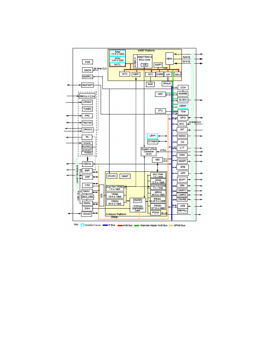
• GEM enhancement for GEA-3
Atlas Ultra-Lite
Atlas Ultra-Lite (referred to herein as AUL) is a power management and user
interface product providing general power, audio, and lighting management
functions. AUL is targeted for the GSM/GPRS/EDGE space for non-applications
processor lineups, but it is protocol independent and may fit other applications
due to its modular functionality.
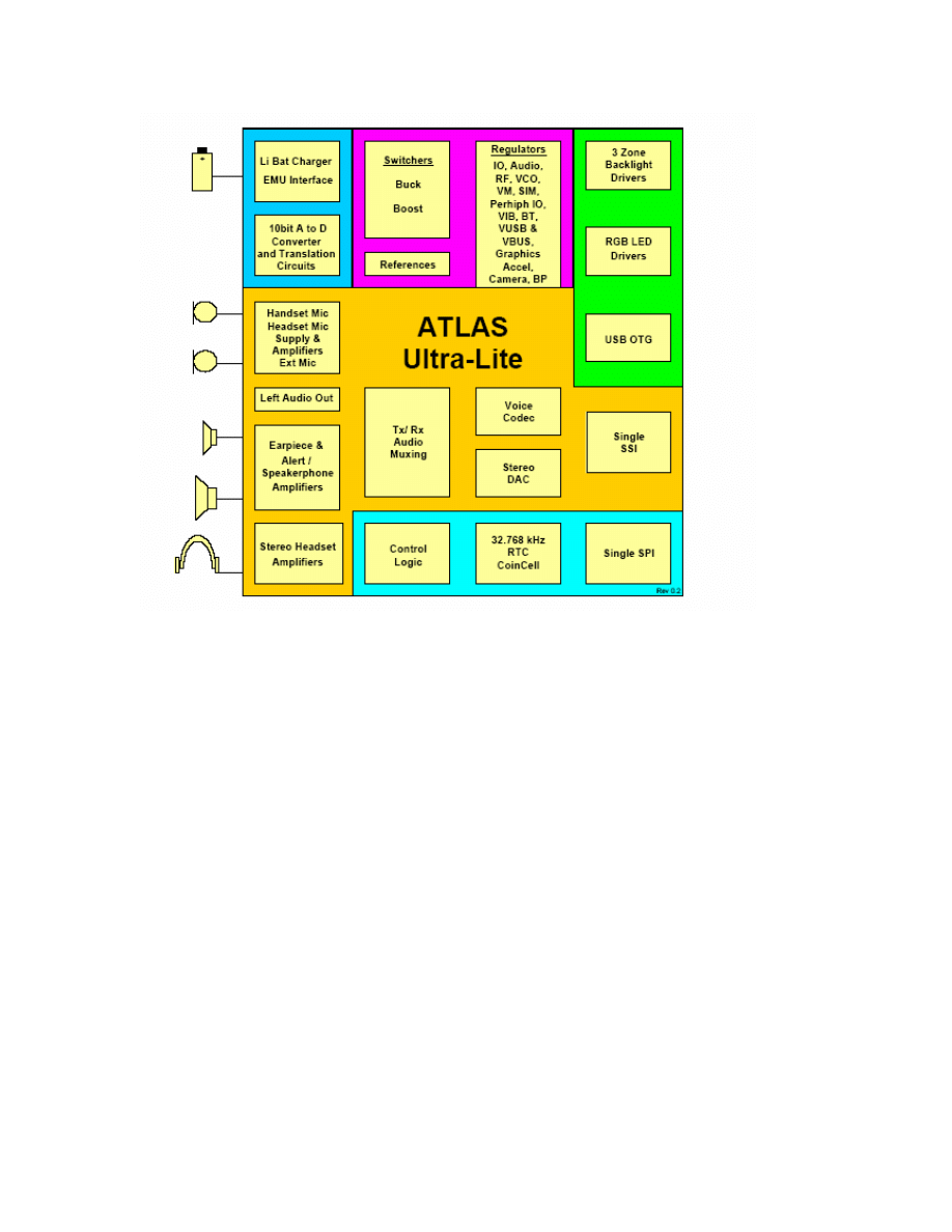
A high level feature list of AUL includes:
- Battery charger with anticipated Enhanced Mini-USB (EMU) charger
capability.
- 10bit ADC for battery monitoring and other readout functions.
- Buck switcher for supply of the processor core, system memory, or other
loading.
- Boost switcher for backlight, fun lights, and USB On-The-Go (OTG) supply.
- LDO regulators with integrated pass devices.
- Transmit amplifiers for handset and headset microphones.
- Receive amplifiers for handset, alert/speaker phone, headset and external
power amps.
- 13bit voice CODEC with both narrow and wide band sampling.
- 16bit stereo DAC supporting multiple sample rates.
- Single SSI audio bus with network mode for connection to multiple devices.
- Power control logic with processor interface and event detection.
- Real time clock and crystal oscillator circuitry.
- Single SPI control bus.
- Three zones of backlight drivers and 3 banks of tri-color driver support with
PWM, ramping, and fun lights control.
- EMU compatible charger path and USB transceiver with CEA936 car kit
support.
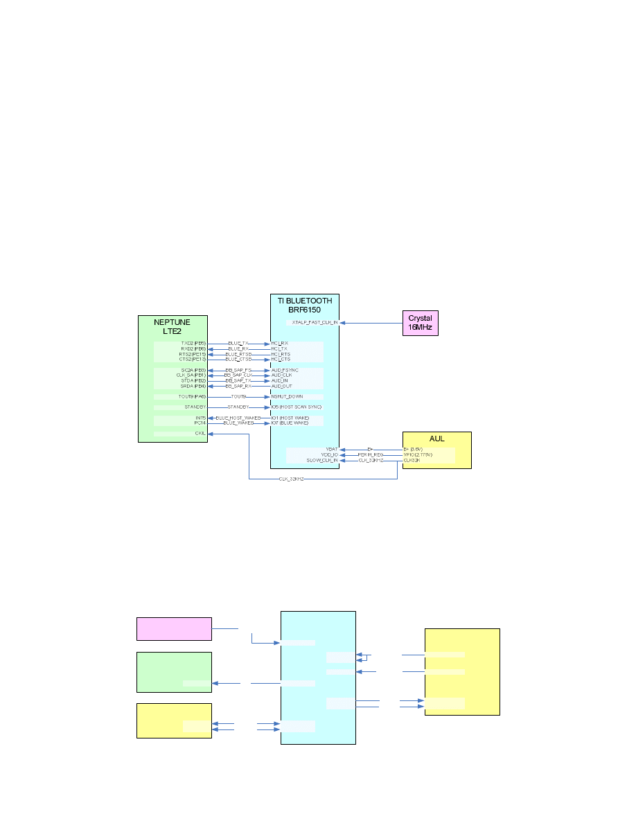
Bluetooth Module
Hawaii Refresh incorporates the TI Bluetooth solution into the overall hardware
design, instead of BCM2035 has been used in many phones design. This design
is based upon a Texas Instruments (TI) BRF6150 single-chip 0.13-µm CMOS
Bluetooth solution. This solution will utilize an embedded ARM7 base-band
microprocessor and an on-chip Digital Radio Processor (DRP) functioning as the
integrated 2.4GHz transceiver. The IC will also comply with Bluetooth core
specification v1.2 and will function as a power class 2 (+4dBm) Bluetooth device.
Hawaii Refresh will be using a dedicated Bluetooth crystal which will provide
16MHz clock signal to the Bluetooth module when the module is enabled.
FM Radio Module
Hawaii Refresh incorporates the SiLabs Si4703 single chip FM radio tuner IC.
This 4x4 mm chip requires only single 2.7~5.5V power supplier, and 32KHz
external clock. The internal frequency synthesizer delivers superior RF
performance, allow to receive FM radio in the range of 76~108MHz.
NEPTUNE
LTE2
PERIPH_REG
INT3
SiLabs
SI4703
FMIP
GPIO2
AUL
VPIO (2.775V)
VA
VD
PERIPH_REG
miniUSB Socket
RCLK
CLK32K
CLK_32KHZ
FM_ANT_IN
CAM_SDA
INT3
PGA_INL
LOUT
ROUT
PGA_INR
PGAINL
PGAINR
ATI W2282
CAM_SCL
CAM_SDA
SCLK
SDIO
CAM_SCL
Memory - Flash/PSRAM
Hawaii Refresh is having external system memory of 512Mbit flash and 128Mbit
PSRAM packaged in a stack part. There are two suppliers for the 512Mb/128Mb
Flash/PSRAM stack part, i.e.:
•
2x256Mb/128Mb STM (M36LLR8870D1ZAQ) stack part. This stack
memory IC two bank of 256 Mbit (16Mx16bit multi-bank multi-level burst)
flash memory and one bank of 128 Mbit (4Mx16bit) pseudo SRAM.
•
2x256Mb/128Mb Intel (PF38F4460) stack part. This stack IC package
contains two monolithic Intel Tyax 256Mb flash part and a 128 Mbit
PSRAM.
Memory MCP
256MbNOR
Tyax
LTE2
AEIM
D[0~15]
EN_WE_F
EN_CE_F1
A[0~23]
EN_OE_F1
F_WP
F_RST
ADV
CLK
WAIT
VCC_F1
VPP_F
VCC_Q
128Mb
PSRAM
D[0~15]
EN_R_DB
EN_R_UB
P1_CS
A[0~22]
EN_R_OE
EN_R_WE
P_CRE
ADV
CLK
WAIT
VCC_P
VCC_Q
256MbNOR
Tyax
D[0~15]
EN_WE_F
EN_OE_F2
A[0~23]
EN_CE_F2
F_WP
F_RST
ADV
CLK
WAIT
VCC_F2
VPP_F
VCC_Q
A[1~24]
D[0~15]
CLK_BURST
LBA
ECB
RESET_OUT
CS0
CS1
CS2
EN_OE
R_W
EN_EB0
EN_EB1
DATA[15:0]
CS0B
CS1B
CS2B
BURSTCLK
LBAB
ECBB
ECBB
ADDRESS24
ADDRESS[24:1]
EB0B
EB1B
RESET_OUT
OEB
R_WB
OEB
VBUCK
VBUCK
VBUCK
Removable Memory Storage
Hawaii Refresh is supporting removable memory storage in the form of microSD
memory card, as well as TransFlash card. The microSD/TransFlash card is
NAND flash based memory card with a form factor of 11mm x 15mm x 1mm.
When used with SD Adapter, the microSD/TransFlash card is compatible with all
existing SD card applications (i.e. PC, digital camera, MP3 player, etc)
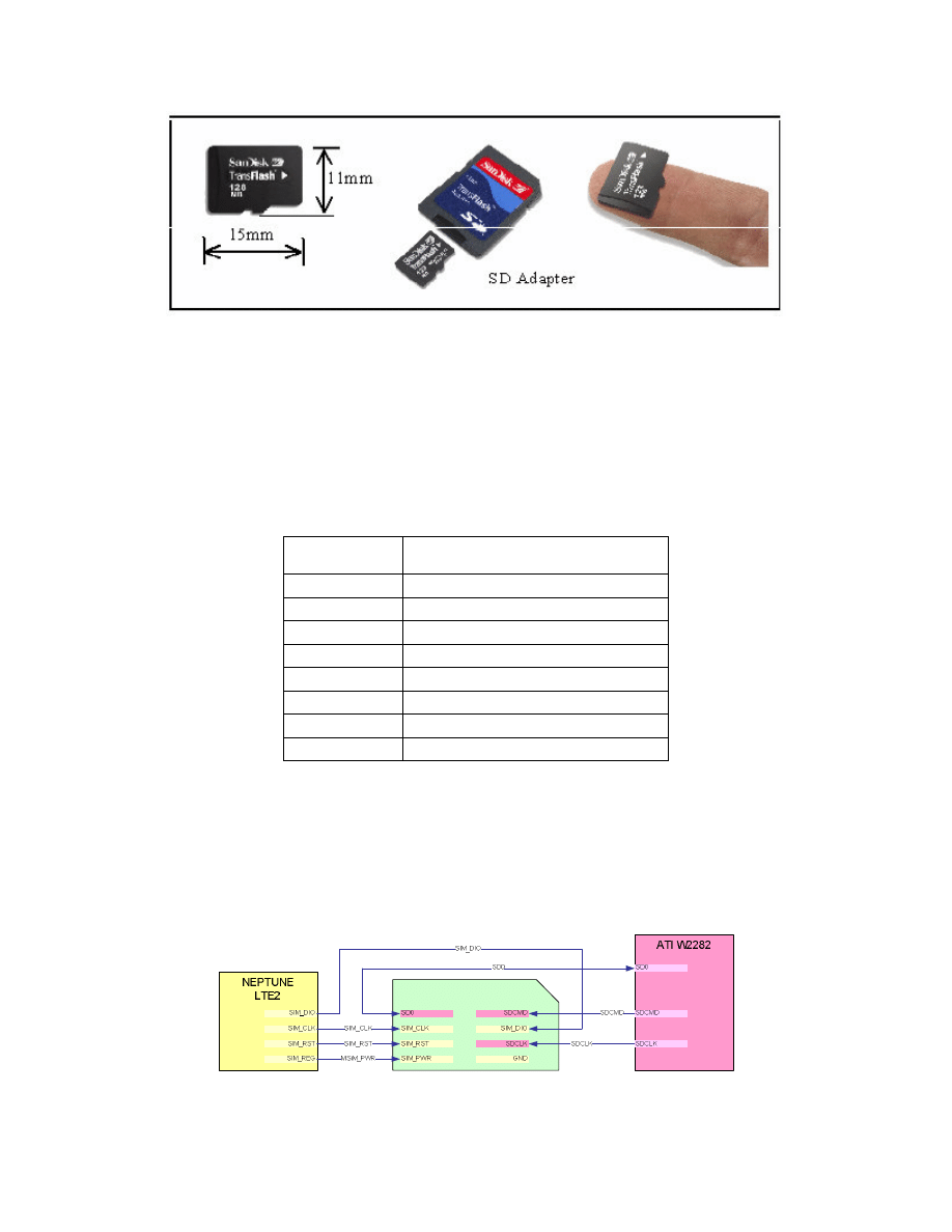
The microSD/TransFlash card communication is based on an 8-pin electrical
interface and it supports Secure Digital (SD) protocol (the same communication
protocol used by SD cards) as well as SPI protocol. The SPI protocol will be
used for communication between LTE2 and microSD/TransFlash card.
Seven different memory capacities are supported, i.e. 16MB, 32MB, 64MB,
128MB, 256MB, 512MB, 1GB and 2GB, with their corresponding Motorola
TransFlash component part number shown below:
Capacity
Motorola Part No.
16MB
8287927W01
32MB
8287928W01
64MB
8287929W01
128MB
8287930W01
256MB
8287931W01
512MB
1GB
2GB
MegaSIM
Hawaii Refresh is supporting 3.0V MegaSIM card with MMC type external
memory storage. Two extra pins SD0, SDCMD are added, and one pin SDCLK
is reused the write protection pin of traditional SIM connector. External memory
interface is shared with TransFlash/microSD interface and controlled by ATI
W2282.
Camera and Display
Hawaii Refresh is supporting 1.9 inch TFT QCIF LCD display, the resolution is
220x176.
Hawaii Refresh is also incorporates a 2MP pixel CMOS camera module. The
camera module sensor and processor is Micron ¼ inch single chip camera
module SOC2020. The resolution is 1600x1200 pixels, and the pixel size is
2.2x2.2 um. The responsivity is 0.53 V/lux-sec, dynamic range 59.5dB and
SNRmax is 37.7dB.
Both LCD and camera module are controlled by ATI GPU W2282.
Camera
Module
ATI W2282
LCD
Module
SS
LCDD[0]~[17]
LS
GS
VIO0CLK
VIO0DATA[0]~[7]
VIP0VSYNC
VIP0HREF
VIP0CLKO
I2C_SCL
I2C_SDA
RGB Data [0]~[17]
GS
OE
LS
DCLK
DCLK
CAM_CLK_OUT
CAM_D[0]~[7]
CAM_VSYNC
CAM_HSYNC
CAM_CLK_IN
CAM_SCL
CAM_SDA
Wyszukiwarka
Podobne podstrony:
Xenon Motherboard theory of operations
(ebook PDF)Shannon A Mathematical Theory Of Communication RXK2WIS2ZEJTDZ75G7VI3OC6ZO2P57GO3E27QNQ
Hawking Theory Of Everything
Maslow (1943) Theory of Human Motivation
Habermas, Jurgen The theory of communicative action Vol 1
Psychology and Cognitive Science A H Maslow A Theory of Human Motivation
Habermas, Jurgen The theory of communicative action Vol 2
Constituents of a theory of media
Luhmann's Systems Theory as a Theory of Modernity
Herrick The History and Theory of Rhetoric (27)
Adeptus Evangelion Base of Operations Record Sheet
Gardner The Theory of Multiple Intelligences
HUME AND?SCARTES ON THE THEORY OF IDEAS
Theory of Varied Consumer Choice?haviour and Its Implicati
Theory of literature MA course 13 dzienni
Krashen's theory of language learning and?quisition
więcej podobnych podstron