
8271GS–AVR–02/2013
Features
•
H
igh Performance, Low Power Atmel
®
AVR
®
8-Bit Microcontroller Family
•
Advanced RISC Architecture
– 131 Powerful Instructions – Most Single Clock Cycle Execution
– 32 x 8 General Purpose Working Registers
– Fully Static Operation
– Up to 20 MIPS Throughput at 20MHz
– On-chip 2-cycle Multiplier
•
High Endurance Non-volatile Memory Segments
– 4/8/16/32KBytes of In-System Self-Programmable Flash program memory
– 256/512/512/1KBytes EEPROM
– 512/1K/1K/2KBytes Internal SRAM
– Write/Erase Cycles: 10,000 Flash/100,000 EEPROM
– Data retention: 20 years at 85
C/100 years at 25C
(1)
– Optional Boot Code Section with Independent Lock Bits
In-System Programming by On-chip Boot Program
True Read-While-Write Operation
– Programming Lock for Software Security
•
Atmel
®
QTouch
®
library support
– Capacitive touch buttons, sliders and wheels
– QTouch and QMatrix
®
acquisition
– Up to 64 sense channels
•
Peripheral Features
– Two 8-bit Timer/Counters with Separate Prescaler and Compare Mode
– One 16-bit Timer/Counter with Separate Prescaler, Compare Mode, and Capture Mode
– Real Time Counter with Separate Oscillator
– Six PWM Channels
– 8-channel 10-bit ADC in TQFP and QFN/MLF package
Temperature Measurement
– 6-channel 10-bit ADC in PDIP Package
Temperature Measurement
– Programmable Serial USART
– Master/Slave SPI Serial Interface
– Byte-oriented 2-wire Serial Interface (Philips I
2
C compatible)
– Programmable Watchdog Timer with Separate On-chip Oscillator
– On-chip Analog Comparator
– Interrupt and Wake-up on Pin Change
•
Special Microcontroller Features
– Power-on Reset and Programmable Brown-out Detection
– Internal Calibrated Oscillator
– External and Internal Interrupt Sources
– Six Sleep Modes: Idle, ADC Noise Reduction, Power-save, Power-down, Standby, and Extended Standby
•
I/O and Packages
– 23 Programmable I/O Lines
– 28-pin PDIP, 32-lead TQFP, 28-pad QFN/MLF and 32-pad QFN/MLF
•
Operating Voltage:
– 1.8 - 5.5V
•
Temperature Range:
– -40
C to 85C
•
Speed Grade:
– 0 - 4MHz@1.8 - 5.5V, 0 - 10MHz@2.7 - 5.5.V, 0 - 20MHz @ 4.5 - 5.5V
•
Power Consumption at 1MHz, 1.8V, 25
C
– Active Mode: 0.2mA
– Power-down Mode: 0.1µA
– Power-save Mode: 0.75µA (Including 32kHz RTC)
Atmel 8-bit Microcontroller with 4/8/16/32KBytes In-
System Programmable Flash
ATmega48A; ATmega48PA; ATmega88A; ATmega88PA;
ATmega168A; ATmega168PA; ATmega328; ATmega328P
SUMMARY
2
ATmega48A/PA/88A/PA/168A/PA/328/P [DATASHEET SUMMARY]
8271GS–AVR–02/2013
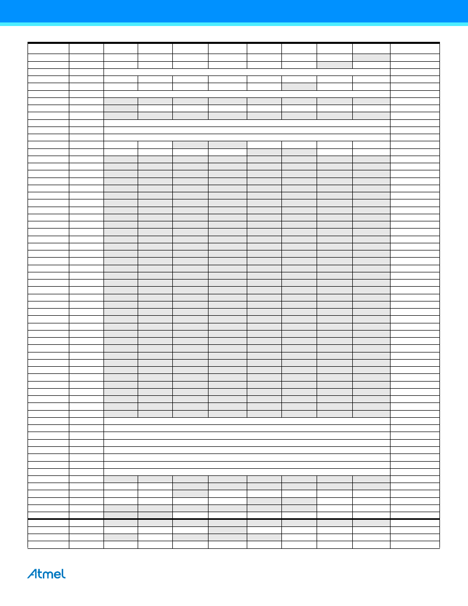
1.
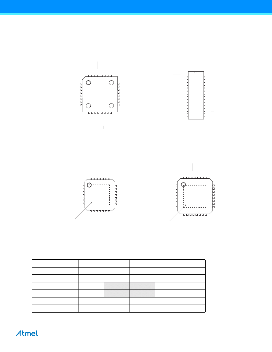
Pin Configurations
Figure 1-1.
Pinout ATmega48A/PA/88A/PA/168A/PA/328/P
1
2
3
4
5
6
7
8
24
23
22
21
20
19
18
17
(PCINT19/OC2B/INT1) PD3
(PCINT20/XCK/T0) PD4
GND
VCC
GND
VCC
(PCINT6/XTAL1/TOSC1) PB6
(PCINT7/XTAL2/TOSC2) PB7
PC1 (ADC1/PCINT9)
PC0 (ADC0/PCINT8)
ADC7
GND
AREF
ADC6
AVCC
PB5 (SCK/PCINT5)
32
31
30
29
28
27
26
25
9
10
11
12
13
14
15
16
(PCINT21/OC0B/T1) PD5
(PCINT22/OC0A/AIN0) PD6
(PCINT23/AIN1) PD7
(PCINT0/CLK
O/ICP1) PB0
(PCINT1/OC1A) PB1
(PCINT2/SS/OC1B) PB2
(PCINT3/OC2A/MOSI) PB3
(PCINT4/MISO) PB4
PD2 (INT0/PCINT18)
PD1 (TXD/PCINT17)
PD0 (RXD/PCINT16)
PC6 (RESET/PCINT14)
PC5 (ADC5/SCL/PCINT13)
PC4 (ADC4/SD
A/PCINT12)
PC3 (ADC3/PCINT11)
PC2 (ADC2/PCINT10)
32 TQFP Top View
1
2
3
4
5
6
7
8
9
10
11
12
13
14
28
27
26
25
24
23
22
21
20
19
18
17
16
15
(PCINT14/RESET) PC6
(PCINT16/RXD) PD0
(PCINT17/TXD) PD1
(PCINT18/INT0) PD2
(PCINT19/OC2B/INT1) PD3
(PCINT20/XCK/T0) PD4
VCC
GND
(PCINT6/XTAL1/TOSC1) PB6
(PCINT7/XTAL2/TOSC2) PB7
(PCINT21/OC0B/T1) PD5
(PCINT22/OC0A/AIN0) PD6
(PCINT23/AIN1) PD7
(PCINT0/CLKO/ICP1) PB0
PC5 (ADC5/SCL/PCINT13)
PC4 (ADC4/SDA/PCINT12)
PC3 (ADC3/PCINT11)
PC2 (ADC2/PCINT10)
PC1 (ADC1/PCINT9)
PC0 (ADC0/PCINT8)
GND
AREF
AVCC
PB5 (SCK/PCINT5)
PB4 (MISO/PCINT4)
PB3 (MOSI/OC2A/PCINT3)
PB2 (SS/OC1B/PCINT2)
PB1 (OC1A/PCINT1)
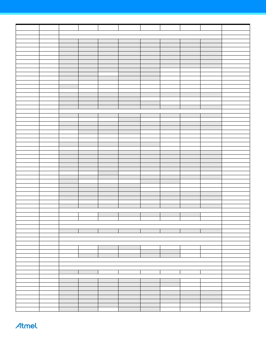
28 PDIP
1
2
3
4
5
6
7
8
24
23
22
21
20
19
18
17
32
31
30
29
28
27
26
25
9
10
11
12
13
14
15
16
32 MLF Top View
(PCINT19/OC2B/INT1) PD3
(PCINT20/XCK/T0) PD4
GND
VCC
GND
VCC
(PCINT6/XTAL1/TOSC1) PB6
(PCINT7/XTAL2/TOSC2) PB7
PC1 (ADC1/PCINT9)
PC0 (ADC0/PCINT8)
ADC7
GND
AREF
ADC6
AVCC
PB5 (SCK/PCINT5)
(PCINT21/OC0B/T1) PD5
(PCINT22/OC0A/AIN0) PD6
(PCINT23/AIN1) PD7
(PCINT0/CLK
O/ICP1) PB0
(PCINT1/OC1A) PB1
(PCINT2/SS/OC1B) PB2
(PCINT3/OC2A/MOSI) PB3
(PCINT4/MISO) PB4
PD2 (INT0/PCINT18)
PD1 (TXD/PCINT17)
PD0 (RXD/PCINT16)
PC6 (RESET/PCINT14)
PC5 (ADC5/SCL/PCINT13)
PC4 (ADC4/SD
A/PCINT12)
PC3 (ADC3/PCINT11)
PC2 (ADC2/PCINT10)
NOTE: Bottom pad should be soldered to ground.
1
2
3
4
5
6
7
21
20
19
18
17
16
15
28
27
26
25
24
23
22
8
9
10
11
12
13
14
28 MLF Top View
(PCINT19/OC2B/INT1) PD3
(PCINT20/XCK/T0) PD4
VCC
GND
(PCINT6/XTAL1/TOSC1) PB6
(PCINT7/XTAL2/TOSC2) PB7
(PCINT21/OC0B/T1) PD5
(PCINT22/OC0A/AIN0) PD6
(PCINT23/AIN1) PD7
(PCINT0/CLK
O/ICP1) PB0
(PCINT1/OC1A) PB1
(PCINT2/SS/OC1B) PB2
(PCINT3/OC2A/MOSI) PB3
(PCINT4/MISO) PB4
PD2 (INT0/PCINT18)
PD1 (TXD/PCINT17)
PD0 (RXD/PCINT16)
PC6 (RESET/PCINT14)
PC5 (ADC5/SCL/PCINT13)
PC4 (ADC4/SD
A/PCINT12)
PC3 (ADC3/PCINT11)
PC2 (ADC2/PCINT10)
PC1 (ADC1/PCINT9)
PC0 (ADC0/PCINT8)
GND
AREF
AVCC
PB5 (SCK/PCINT5)
NOTE: Bottom pad should be soldered to ground.
Table 1-1.
32UFBGA - Pinout ATmega48A/48PA/88A/88PA/168A/168PA
1
2
3
4
5
6
A
PD2
PD1
PC6
PC4
PC2
PC1
B
PD3
PD4
PD0
PC5
PC3
PC0
C
GND
GND
ADC7
GND
D
VDD
VDD
AREF
ADC6
E
PB6
PD6
PB0
PB2
AVDD
PB5
F
PB7
PD5
PD7
PB1
PB3
PB4

3
ATmega48A/PA/88A/PA/168A/PA/328/P [DATASHEET SUMMARY]
8271GS–AVR–02/2013
1.1
Pin Descriptions
1.1.1
VCC
Digital supply voltage.
1.1.2
GND
Ground.
1.1.3
Port B (PB7:0) XTAL1/XTAL2/TOSC1/TOSC2
Port B is an 8-bit bi-directional I/O port with internal pull-up resistors (selected for each bit). The Port B output buf-
fers have symmetrical drive characteristics with both high sink and source capability. As inputs, Port B pins that are
externally pulled low will source current if the pull-up resistors are activated. The Port B pins are tri-stated when a
reset condition becomes active, even if the clock is not running.
Depending on the clock selection fuse settings, PB6 can be used as input to the inverting Oscillator amplifier and
input to the internal clock operating circuit.
Depending on the clock selection fuse settings, PB7 can be used as output from the inverting Oscillator amplifier.
If the Internal Calibrated RC Oscillator is used as chip clock source, PB7...6 is used as TOSC2...1 input for the
Asynchronous Timer/Counter2 if the AS2 bit in ASSR is set.
The various special features of Port B are elaborated in
”Alternate Functions of Port B” on page 83
and
”System
Clock and Clock Options” on page 26
.
1.1.4
Port C (PC5:0)
Port C is a 7-bit bi-directional I/O port with internal pull-up resistors (selected for each bit). The PC5...0 output buf-
fers have symmetrical drive characteristics with both high sink and source capability. As inputs, Port C pins that are
externally pulled low will source current if the pull-up resistors are activated. The Port C pins are tri-stated when a
reset condition becomes active, even if the clock is not running.
1.1.5
PC6/RESET
If the RSTDISBL Fuse is programmed, PC6 is used as an I/O pin. Note that the electrical characteristics of PC6 dif-
fer from those of the other pins of Port C.
If the RSTDISBL Fuse is unprogrammed, PC6 is used as a Reset input. A low level on this pin for longer than the
minimum pulse length will generate a Reset, even if the clock is not running. The minimum pulse length is given in
Table 29-12 on page 310
. Shorter pulses are not guaranteed to generate a Reset.
The various special features of Port C are elaborated in
”Alternate Functions of Port C” on page 86
.
1.1.6
Port D (PD7:0)
Port D is an 8-bit bi-directional I/O port with internal pull-up resistors (selected for each bit). The Port D output buf-
fers have symmetrical drive characteristics with both high sink and source capability. As inputs, Port D pins that are
externally pulled low will source current if the pull-up resistors are activated. The Port D pins are tri-stated when a
reset condition becomes active, even if the clock is not running.
The various special features of Port D are elaborated in
”Alternate Functions of Port D” on page 89
.
1.1.7
AV
CC
AV
CC
is the supply voltage pin for the A/D Converter, PC3:0, and ADC7:6. It should be externally connected to V
CC
,
even if the ADC is not used. If the ADC is used, it should be connected to V
CC
through a low-pass filter. Note that
PC6...4 use digital supply voltage, V
CC
.

4
ATmega48A/PA/88A/PA/168A/PA/328/P [DATASHEET SUMMARY]
8271GS–AVR–02/2013
1.1.8
AREF
AREF is the analog reference pin for the A/D Converter.
1.1.9
ADC7:6 (TQFP and QFN/MLF Package Only)
In the TQFP and QFN/MLF package, ADC7:6 serve as analog inputs to the A/D converter. These pins are powered
from the analog supply and serve as 10-bit ADC channels.
5
ATmega48A/PA/88A/PA/168A/PA/328/P [DATASHEET SUMMARY]
8271GS–AVR–02/2013
2.
Overview
The ATmega48A/PA/88A/PA/168A/PA/328/P is a low-power CMOS 8-bit microcontroller based on the AVR
e n h a n c e d R I S C a r c h i t e c t u r e . B y e x e c u t i n g p o w e r f u l i n s t r u c t i o n s i n a s i n g l e c l o c k c y c l e , t h e
ATmega48A/PA/88A/PA/168A/PA/328/P achieves throughputs approaching 1 MIPS per MHz allowing the system
designer to optimize power consumption versus processing speed.
2.1
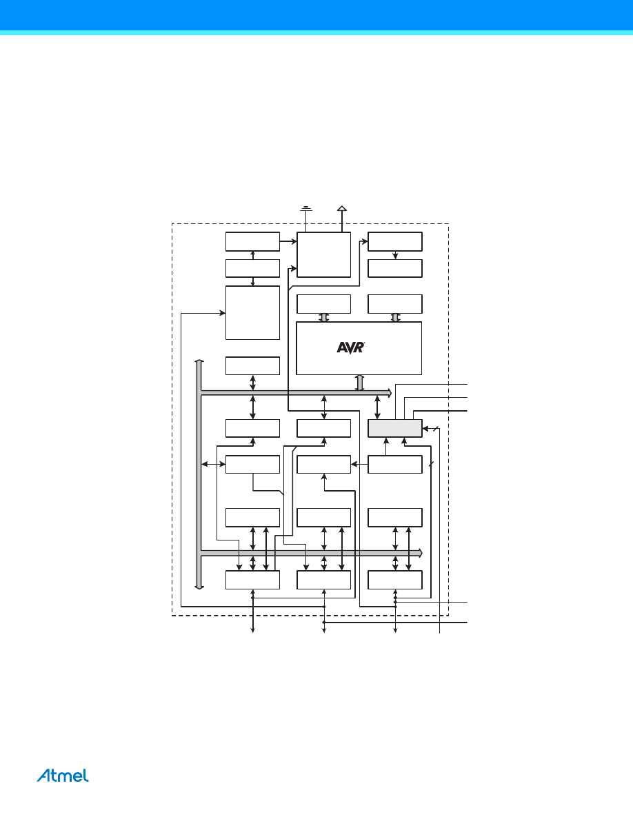
Block Diagram
Figure 2-1.
Block Diagram
The AVR core combines a rich instruction set with 32 general purpose working registers. All the 32 registers are
directly connected to the Arithmetic Logic Unit (ALU), allowing two independent registers to be accessed in one
single instruction executed in one clock cycle. The resulting architecture is more code efficient while achieving
throughputs up to ten times faster than conventional CISC microcontrollers.
PORT C (7)
PORT B (8)
PORT D (8)
USART 0
8bit T/C 2
16bit T/C 1
8bit T/C 0
A/D Conv.
Internal
Bandgap
Analog
Comp.
SPI
TWI
SRAM
Flash
EEPROM
Watchdog
Oscillator
Watchdog
Timer
Oscillator
Circuits /
Clock
Generation
Power
Supervision
POR / BOD &
RESET
VCC
GND
PROGRAM
LOGIC
debugWIRE
2
GND
AREF
AVCC
D
ATA
B
U
S
ADC[6..7]
PC[0..6]
PB[0..7]
PD[0..7]
6
RESET
XTAL[1..2]
CPU
6
ATmega48A/PA/88A/PA/168A/PA/328/P [DATASHEET SUMMARY]
8271GS–AVR–02/2013
The ATmega48A/PA/88A/PA/168A/PA/328/P provides the following features: 4K/8Kbytes of In-System Program-
mable Flash with Read-While-Write capabilities, 256/512/512/1Kbytes EEPROM, 512/1K/1K/2Kbytes SRAM,
23 general purpose I/O lines, 32 general purpose working registers, three flexible Timer/Counters with compare
modes, internal and external interrupts, a serial programmable USART, a byte-oriented 2-wire Serial Interface, an
SPI serial port, a 6-channel 10-bit ADC (8 channels in TQFP and QFN/MLF packages), a programmable Watchdog
Timer with internal Oscillator, and five software selectable power saving modes. The Idle mode stops the CPU
while allowing the SRAM, Timer/Counters, USART, 2-wire Serial Interface, SPI port, and interrupt system to con-
tinue functioning. The Power-down mode saves the register contents but freezes the Oscillator, disabling all other
chip functions until the next interrupt or hardware reset. In Power-save mode, the asynchronous timer continues to
run, allowing the user to maintain a timer base while the rest of the device is sleeping. The ADC Noise Reduction
mode stops the CPU and all I/O modules except asynchronous timer and ADC, to minimize switching noise during
ADC conversions. In Standby mode, the crystal/resonator Oscillator is running while the rest of the device is sleep-
ing. This allows very fast start-up combined with low power consumption.
Atmel
®
offers the QTouch
®
library for embedding capacitive touch buttons, sliders and wheels functionality into
AVR
®
microcontrollers. The patented charge-transfer signal acquisition offers robust sensing and includes fully
debounced reporting of touch keys and includes Adjacent Key Suppression
®
(AKS
™
) technology for unambiguous
detection of key events. The easy-to-use QTouch Suite toolchain allows you to explore, develop and debug your
own touch applications.
The device is manufactured using Atmel’s high density non-volatile memory technology. The On-chip ISP Flash
allows the program memory to be reprogrammed In-System through an SPI serial interface, by a conventional non-
volatile memory programmer, or by an On-chip Boot program running on the AVR core. The Boot program can use
any interface to download the application program in the Application Flash memory. Software in the Boot Flash
section will continue to run while the Application Flash section is updated, providing true Read-While-Write opera-
tion. By combining an 8-bit RISC CPU with In-System Self-Programmable Flash on a monolithic chip, the Atmel
ATmega48A/PA/88A/PA/168A/PA/328/P is a powerful microcontroller that provides a highly flexible and cost effec-
tive solution to many embedded control applications.
The ATmega48A/PA/88A/PA/168A/PA/328/P AVR is supported with a full suite of program and system develop-
ment tools including: C Compilers, Macro Assemblers, Program Debugger/Simulators, In-Circuit Emulators, and
Evaluation kits.
2.2
Comparison Between Processors
The ATmega48A/PA/88A/PA/168A/PA/328/P differ only in memory sizes, boot loader support, and interrupt vector
sizes.
Table 2-1
summarizes the different memory and interrupt vector sizes for the devices.
ATmega48A/PA/88A/PA/168A/PA/328/P support a real Read-While-Write Self-Programming mechanism. There is
a separate Boot Loader Section, and the SPM instruction can only execute from there. In ATmega 48A/48PA there
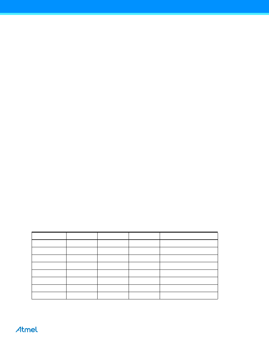
Table 2-1.
Memory Size Summary
Device
Flash
EEPROM
RAM
Interrupt Vector Size
ATmega48A
4KBytes
256Bytes
512Bytes
1 instruction word/vector
ATmega48PA
4KBytes
256Bytes
512Bytes
1 instruction word/vector
ATmega88A
8KBytes
512Bytes
1KBytes
1 instruction word/vector
ATmega88PA
8KBytes
512Bytes
1KBytes
1 instruction word/vector
ATmega168A
16KBytes
512Bytes
1KBytes
2 instruction words/vector
ATmega168PA
16KBytes
512Bytes
1KBytes
2 instruction words/vector
ATmega328
32KBytes
1KBytes
2KBytes
2 instruction words/vector
ATmega328P
32KBytes
1KBytes
2KBytes
2 instruction words/vector

7
ATmega48A/PA/88A/PA/168A/PA/328/P [DATASHEET SUMMARY]
8271GS–AVR–02/2013
is no Read-While-Write support and no separate Boot Loader Section. The SPM instruction can execute from the
entire Flash
3.
Resources
A comprehensive set of development tools, application notes and datasheets are available for download on
http://www.atmel.com/avr.
Note:
1.
4.
Data Retention
Reliability Qualification results show that the projected data retention failure rate is much less than 1 PPM over 20
years at 85°C or 100 years at 25°C.
5.
About Code Examples
This documentation contains simple code examples that briefly show how to use various parts of the device. These
code examples assume that the part specific header file is included before compilation. Be aware that not all C
compiler vendors include bit definitions in the header files and interrupt handling in C is compiler dependent.
Please confirm with the C compiler documentation for more details.
For I/O Registers located in extended I/O map, “IN”, “OUT”, “SBIS”, “SBIC”, “CBI”, and “SBI” instructions must be
replaced with instructions that allow access to extended I/O. Typically “LDS” and “STS” combined with “SBRS”,
“SBRC”, “SBR”, and “CBR”.
6.
Capacitive Touch Sensing
The Atmel
®
QTouch
®
Library provides a simple to use solution to realize touch sensitive interfaces on most Atmel
AVR
®
microcontrollers. The QTouch Library includes support for the Atmel QTouch and Atmel QMatrix
®
acquisition
methods.
Touch sensing can be added to any application by linking the appropriate Atmel QTouch Library for the AVR Micro-
controller. This is done by using a simple set of APIs to define the touch channels and sensors, and then calling the
touch sensing API’s to retrieve the channel information and determine the touch sensor states.
The QTouch Library is FREE and downloadable from the Atmel website at the following location:
. For implementation details and other information, refer to the
Atmel QTouch Library
User Guide
- also available for download from Atmel website.
8
ATmega48A/PA/88A/PA/168A/PA/328/P [DATASHEET SUMMARY]
8271GS–AVR–02/2013
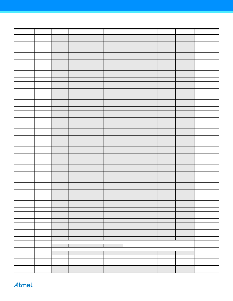
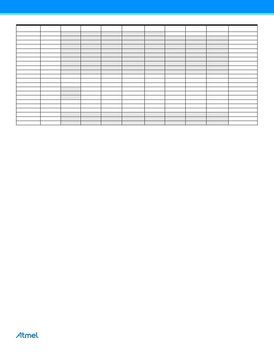
7.
Register Summary
Address
Name
Bit 7
Bit 6
Bit 5
Bit 4
Bit 3
Bit 2
Bit 1
Bit 0
Page
(0xFF)
Reserved
–
–
–
–
–
–
–
–
(0xFE)
Reserved
–
–
–
–
–
–
–
–
(0xFD)
Reserved
–
–
–
–
–
–
–
–
(0xFC)
Reserved
–
–
–
–
–
–
–
–
(0xFB)
Reserved
–
–
–
–
–
–
–
–
(0xFA)
Reserved
–
–
–
–
–
–
–
–
(0xF9)
Reserved
–
–
–
–
–
–
–
–
(0xF8)
Reserved
–
–
–
–
–
–
–
–
(0xF7)
Reserved
–
–
–
–
–
–
–
–
(0xF6)
Reserved
–
–
–
–
–
–
–
–
(0xF5)
Reserved
–
–
–
–
–
–
–
–
(0xF4)
Reserved
–
–
–
–
–
–
–
–
(0xF3)
Reserved
–
–
–
–
–
–
–
–
(0xF2)
Reserved
–
–
–
–
–
–
–
–
(0xF1)
Reserved
–
–
–
–
–
–
–
–
(0xF0)
Reserved
–
–
–
–
–
–
–
–
(0xEF)
Reserved
–
–
–
–
–
–
–
–
(0xEE)
Reserved
–
–
–
–
–
–
–
–
(0xED)
Reserved
–
–
–
–
–
–
–
–
(0xEC)
Reserved
–
–
–
–
–
–
–
–
(0xEB)
Reserved
–
–
–
–
–
–
–
–
(0xEA)
Reserved
–
–
–
–
–
–
–
–
(0xE9)
Reserved
–
–
–
–
–
–
–
–
(0xE8)
Reserved
–
–
–
–
–
–
–
–
(0xE7)
Reserved
–
–
–
–
–
–
–
–
(0xE6)
Reserved
–
–
–
–
–
–
–
–
(0xE5)
Reserved
–
–
–
–
–
–
–
–
(0xE4)
Reserved
–
–
–
–
–
–
–
–
(0xE3)
Reserved
–
–
–
–
–
–
–
–
(0xE2)
Reserved
–
–
–
–
–
–
–
–
(0xE1)
Reserved
–
–
–
–
–
–
–
–
(0xE0)
Reserved
–
–
–
–
–
–
–
–
(0xDF)
Reserved
–
–
–
–
–
–
–
–
(0xDE)
Reserved
–
–
–
–
–
–
–
–
(0xDD)
Reserved
–
–
–
–
–
–
–
–
(0xDC)
Reserved
–
–
–
–
–
–
–
–
(0xDB)
Reserved
–
–
–
–
–
–
–
–
(0xDA)
Reserved
–
–
–
–
–
–
–
–
(0xD9)
Reserved
–
–
–
–
–
–
–
–
(0xD8)
Reserved
–
–
–
–
–
–
–
–
(0xD7)
Reserved
–
–
–
–
–
–
–
–
(0xD6)
Reserved
–
–
–
–
–
–
–
–
(0xD5)
Reserved
–
–
–
–
–
–
–
–
(0xD4)
Reserved
–
–
–
–
–
–
–
–
(0xD3)
Reserved
–
–
–
–
–
–
–
–
(0xD2)
Reserved
–
–
–
–
–
–
–
–
(0xD1)
Reserved
–
–
–
–
–
–
–
–
(0xD0)
Reserved
–
–
–
–
–
–
–
–
(0xCF)
Reserved
–
–
–
–
–
–
–
–
(0xCE)
Reserved
–
–
–
–
–
–
–
–
(0xCD)
Reserved
–
–
–
–
–
–
–
–
(0xCC)
Reserved
–
–
–
–
–
–
–
–
(0xCB)
Reserved
–
–
–
–
–
–
–
–
(0xCA)
Reserved
–
–
–
–
–
–
–
–
(0xC9)
Reserved
–
–
–
–
–
–
–
–
(0xC8)
Reserved
–
–
–
–
–
–
–
–
(0xC7)
Reserved
–
–
–
–
–
–
–
–
(0xC6)
UDR0
USART I/O Data Register
194
(0xC5)
UBRR0H
USART Baud Rate Register High
198
(0xC4)
UBRR0L
USART Baud Rate Register Low
198
(0xC3)
Reserved
–
–
–
–
–
–
–
–
(0xC2)
UCSR0C
UMSEL01
UMSEL00
UPM01
UPM00
USBS0
UCSZ01 /UDORD0
UCSZ00 / UCPHA0
UCPOL0
196/207
(0xC1)
UCSR0B
RXCIE0
TXCIE0
UDRIE0
RXEN0
TXEN0
UCSZ02
RXB80
TXB80
195
(0xC0)
UCSR0A
RXC0
TXC0
UDRE0
FE0
DOR0
UPE0
U2X0
MPCM0
194
(0xBF)
Reserved
–
–
–
–
–
–
–
–
(0xBE)
Reserved
–
–
–
–
–
–
–
–
9
ATmega48A/PA/88A/PA/168A/PA/328/P [DATASHEET SUMMARY]
8271GS–AVR–02/2013
(0xBD)
TWAMR
TWAM6
TWAM5
TWAM4
TWAM3
TWAM2
TWAM1
TWAM0
–
237
(0xBC)
TWCR
TWINT
TWEA
TWSTA
TWSTO
TWWC
TWEN
–
TWIE
235
(0xBB)
TWDR
2-wire Serial Interface Data Register
237
(0xBA)
TWAR
TWA6
TWA5
TWA4
TWA3
TWA2
TWA1
TWA0
TWGCE
237
(0xB9)
TWSR
TWS7
TWS6
TWS5
TWS4
TWS3
–
TWPS1
TWPS0
236
(0xB8)
TWBR
2-wire Serial Interface Bit Rate Register
235
(0xB7)
Reserved
–
–
–
–
–
–
–
(0xB6)
ASSR
–
EXCLK
AS2
TCN2UB
OCR2AUB
OCR2BUB
TCR2AUB
TCR2BUB
160
(0xB5)
Reserved
–
–
–
–
–
–
–
–
(0xB4)
OCR2B
Timer/Counter2 Output Compare Register B
159
(0xB3)
OCR2A
Timer/Counter2 Output Compare Register A
159
(0xB2)
TCNT2
Timer/Counter2 (8-bit)
159
(0xB1)
TCCR2B
FOC2A
FOC2B
–
–
WGM22
CS22
CS21
CS20
158
(0xB0)
TCCR2A
COM2A1
COM2A0
COM2B1
COM2B0
–
–
WGM21
WGM20
155
(0xAF)
Reserved
–
–
–
–
–
–
–
–
(0xAE)
Reserved
–
–
–
–
–
–
–
–
(0xAD)
Reserved
–
–
–
–
–
–
–
–
(0xAC)
Reserved
–
–
–
–
–
–
–
–
(0xAB)
Reserved
–
–
–
–
–
–
–
–
(0xAA)
Reserved
–
–
–
–
–
–
–
–
(0xA9)
Reserved
–
–
–
–
–
–
–
–
(0xA8)
Reserved
–
–
–
–
–
–
–
–
(0xA7)
Reserved
–
–
–
–
–
–
–
–
(0xA6)
Reserved
–
–
–
–
–
–
–
–
(0xA5)
Reserved
–
–
–
–
–
–
–
–
(0xA4)
Reserved
–
–
–
–
–
–
–
–
(0xA3)
Reserved
–
–
–
–
–
–
–
–
(0xA2)
Reserved
–
–
–
–
–
–
–
–
(0xA1)
Reserved
–
–
–
–
–
–
–
–
(0xA0)
Reserved
–
–
–
–
–
–
–
–
(0x9F)
Reserved
–
–
–
–
–
–
–
–
(0x9E)
Reserved
–
–
–
–
–
–
–
–
(0x9D)
Reserved
–
–
–
–
–
–
–
–
(0x9C)
Reserved
–
–
–
–
–
–
–
–
(0x9B)
Reserved
–
–
–
–
–
–
–
–
(0x9A)
Reserved
–
–
–
–
–
–
–
–
(0x99)
Reserved
–
–
–
–
–
–
–
–
(0x98)
Reserved
–
–
–
–
–
–
–
–
(0x97)
Reserved
–
–
–
–
–
–
–
–
(0x96)
Reserved
–
–
–
–
–
–
–
–
(0x95)
Reserved
–
–
–
–
–
–
–
–
(0x94)
Reserved
–
–
–
–
–
–
–
–
(0x93)
Reserved
–
–
–
–
–
–
–
–
(0x92)
Reserved
–
–
–
–
–
–
–
–
(0x91)
Reserved
–
–
–
–
–
–
–
–
(0x90)
Reserved
–
–
–
–
–
–
–
–
(0x8F)
Reserved
–
–
–
–
–
–
–
–
(0x8E)
Reserved
–
–
–
–
–
–
–
–
(0x8D)
Reserved
–
–
–
–
–
–
–
–
(0x8C)
Reserved
–
–
–
–
–
–
–
–
(0x8B)
OCR1BH
Timer/Counter1 - Output Compare Register B High Byte
136
(0x8A)
OCR1BL
Timer/Counter1 - Output Compare Register B Low Byte
136
(0x89)
OCR1AH
Timer/Counter1 - Output Compare Register A High Byte
136
(0x88)
OCR1AL
Timer/Counter1 - Output Compare Register A Low Byte
136
(0x87)
ICR1H
Timer/Counter1 - Input Capture Register High Byte
136
(0x86)
ICR1L
Timer/Counter1 - Input Capture Register Low Byte
136
(0x85)
TCNT1H
Timer/Counter1 - Counter Register High Byte
135
(0x84)
TCNT1L
Timer/Counter1 - Counter Register Low Byte
135
(0x83)
Reserved
–
–
–
–
–
–
–
–
(0x82)
TCCR1C
FOC1A
FOC1B
–
–
–
–
–
–
135
(0x81)
TCCR1B
ICNC1
ICES1
–
WGM13
WGM12
CS12
CS11
CS10
134
(0x80)
TCCR1A
COM1A1
COM1A0
COM1B1
COM1B0
–
–
WGM11
WGM10
132
(0x7F)
DIDR1
–
–
–
–
–
–
AIN1D
AIN0D
241
(0x7E)
DIDR0
–
–
ADC5D
ADC4D
ADC3D
ADC2D
ADC1D
ADC0D
257
(0x7D)
Reserved
–
–
–
–
–
–
–
–
(0x7C)
ADMUX
REFS1
REFS0
ADLAR
–
MUX3
MUX2
MUX1
MUX0
254
(0x7B)
ADCSRB
–
ACME
–
–
–
ADTS2
ADTS1
ADTS0
257
(0x7A)
ADCSRA
ADEN
ADSC
ADATE
ADIF
ADIE
ADPS2
ADPS1
ADPS0
255
Address
Name
Bit 7
Bit 6
Bit 5
Bit 4
Bit 3
Bit 2
Bit 1
Bit 0
Page
10
ATmega48A/PA/88A/PA/168A/PA/328/P [DATASHEET SUMMARY]
8271GS–AVR–02/2013
(0x79)
ADCH
ADC Data Register High byte
256
(0x78)
ADCL
ADC Data Register Low byte
256
(0x77)
Reserved
–
–
–
–
–
–
–
–
(0x76)
Reserved
–
–
–
–
–
–
–
–
(0x75)
Reserved
–
–
–
–
–
–
–
–
(0x74)
Reserved
–
–
–
–
–
–
–
–
(0x73)
Reserved
–
–
–
–
–
–
–
–
(0x72)
Reserved
–
–
–
–
–
–
–
–
(0x71)
Reserved
–
–
–
–
–
–
–
–
(0x70)
TIMSK2
–
–
–
–
–
OCIE2B
OCIE2A
TOIE2
159
(0x6F)
TIMSK1
–
–
ICIE1
–
–
OCIE1B
OCIE1A
TOIE1
136
(0x6E)
TIMSK0
–
–
–
–
–
OCIE0B
OCIE0A
TOIE0
110
(0x6D)
PCMSK2
PCINT23
PCINT22
PCINT21
PCINT20
PCINT19
PCINT18
PCINT17
PCINT16
75
(0x6C)
PCMSK1
–
PCINT14
PCINT13
PCINT12
PCINT11
PCINT10
PCINT9
PCINT8
75
(0x6B)
PCMSK0
PCINT7
PCINT6
PCINT5
PCINT4
PCINT3
PCINT2
PCINT1
PCINT0
75
(0x6A)
Reserved
–
–
–
–
–
–
–
–
(0x69)
EICRA
–
–
–
–
ISC11
ISC10
ISC01
ISC00
72
(0x68)
PCICR
–
–
–
–
–
PCIE2
PCIE1
PCIE0
(0x67)
Reserved
–
–
–
–
–
–
–
–
(0x66)
OSCCAL
Oscillator Calibration Register
36
(0x65)
Reserved
–
–
–
–
–
–
–
–
(0x64)
PRR
PRTWI
PRTIM2
PRTIM0
–
PRTIM1
PRSPI
PRUSART0
PRADC
41
(0x63)
Reserved
–
–
–
–
–
–
–
–
(0x62)
Reserved
–
–
–
–
–
–
–
–
(0x61)
CLKPR
CLKPCE
–
–
–
CLKPS3
CLKPS2
CLKPS1
CLKPS0
36
(0x60)
WDTCSR
WDIF
WDIE
WDP3
WDCE
WDE
WDP2
WDP1
WDP0
54
0x3F (0x5F)
SREG
I
T
H
S
V
N
Z
C
9
0x3E (0x5E)
SPH
–
–
–
–
–
(SP10)
5.
SP9
SP8
12
0x3D (0x5D)
SPL
SP7
SP6
SP5
SP4
SP3
SP2
SP1
SP0
12
0x3C (0x5C)
Reserved
–
–
–
–
–
–
–
–
0x3B (0x5B)
Reserved
–
–
–
–
–
–
–
–
0x3A (0x5A)
Reserved
–
–
–
–
–
–
–
–
0x39 (0x59)
Reserved
–
–
–
–
–
–
–
–
0x38 (0x58)
Reserved
–
–
–
–
–
–
–
–
0x37 (0x57)
SPMCSR
SPMIE
(RWWSB)
5.
SIGRD
(RWWSRE)
5.
BLBSET
PGWRT
PGERS
SPMEN
283
0x36 (0x56)
Reserved
–
–
–
–
–
–
–
–
0x35 (0x55)
MCUCR
–
BODS
(6)
BODSE
(6)
PUD
–
–
IVSEL
IVCE
44/69/92
0x34 (0x54)
MCUSR
–
–
–
–
WDRF
BORF
EXTRF
PORF
54
0x33 (0x53)
SMCR
–
–
–
–
SM2
SM1
SM0
SE
39
0x32 (0x52)
Reserved
–
–
–
–
–
–
–
–
0x31 (0x51)
Reserved
–
–
–
–
–
–
–
–
0x30 (0x50)
ACSR
ACD
ACBG
ACO
ACI
ACIE
ACIC
ACIS1
ACIS0
240
0x2F (0x4F)
Reserved
–
–
–
–
–
–
–
–
0x2E (0x4E)
SPDR
SPI Data Register
171
0x2D (0x4D)
SPSR
SPIF
WCOL
–
–
–
–
–
SPI2X
170
0x2C (0x4C)
SPCR
SPIE
SPE
DORD
MSTR
CPOL
CPHA
SPR1
SPR0
169
0x2B (0x4B)
GPIOR2
General Purpose I/O Register 2
25
0x2A (0x4A)
GPIOR1
General Purpose I/O Register 1
25
0x29 (0x49)
Reserved
–
–
–
–
–
–
–
–
0x28 (0x48)
OCR0B
Timer/Counter0 Output Compare Register B
0x27 (0x47)
OCR0A
Timer/Counter0 Output Compare Register A
0x26 (0x46)
TCNT0
Timer/Counter0 (8-bit)
0x25 (0x45)
TCCR0B
FOC0A
FOC0B
–
–
WGM02
CS02
CS01
CS00
0x24 (0x44)
TCCR0A
COM0A1
COM0A0
COM0B1
COM0B0
–
–
WGM01
WGM00
0x23 (0x43)
GTCCR
TSM
–
–
–
–
–
PSRASY
PSRSYNC
141/161
0x22 (0x42)
EEARH
(EEPROM Address Register High Byte)
5.
21
0x21 (0x41)
EEARL
EEPROM Address Register Low Byte
21
0x20 (0x40)
EEDR
EEPROM Data Register
21
0x1F (0x3F)
EECR
–
–
EEPM1
EEPM0
EERIE
EEMPE
EEPE
EERE
21
0x1E (0x3E)
GPIOR0
General Purpose I/O Register 0
25
0x1D (0x3D)
EIMSK
–
–
–
–
–
–
INT1
INT0
73
0x1C (0x3C)
EIFR
–
–
–
–
–
–
INTF1
INTF0
73
0x1B (0x3B)
PCIFR
–
–
–
–
–
PCIF2
PCIF1
PCIF0
0x1A (0x3A)
Reserved
–
–
–
–
–
–
–
–
0x19 (0x39)
Reserved
–
–
–
–
–
–
–
–
0x18 (0x38)
Reserved
–
–
–
–
–
–
–
–
0x17 (0x37)
TIFR2
–
–
–
–
–
OCF2B
OCF2A
TOV2
160
0x16 (0x36)
TIFR1
–
–
ICF1
–
–
OCF1B
OCF1A
TOV1
137
Address
Name
Bit 7
Bit 6
Bit 5
Bit 4
Bit 3
Bit 2
Bit 1
Bit 0
Page
11
ATmega48A/PA/88A/PA/168A/PA/328/P [DATASHEET SUMMARY]
8271GS–AVR–02/2013
Note:
1. For compatibility with future devices, reserved bits should be written to zero if accessed. Reserved I/O memory addresses
should never be written.
2. I/O Registers within the address range 0x00 - 0x1F are directly bit-accessible using the SBI and CBI instructions. In these
registers, the value of single bits can be checked by using the SBIS and SBIC instructions.
3. Some of the Status Flags are cleared by writing a logical one to them. Note that, unlike most other AVRs, the CBI and SBI
instructions will only operate on the specified bit, and can therefore be used on registers containing such Status Flags. The
CBI and SBI instructions work with registers 0x00 to 0x1F only.
4. When using the I/O specific commands IN and OUT, the I/O addresses 0x00 - 0x3F must be used. When addressing I/O
Registers as data space using LD and ST instructions, 0x20 must be added to these addresses. The
ATmega48A/PA/88A/PA/168A/PA/328/P is a complex microcontroller with more peripheral units than can be supported
within the 64 location reserved in Opcode for the IN and OUT instructions. For the Extended I/O space from 0x60 - 0xFF in
SRAM, only the ST/STS/STD and LD/LDS/LDD instructions can be used.
5. Only valid for ATmega88A/88PA/168A/168PA/328/328P.
6. BODS and BODSE only available for picoPower devices ATmega48PA/88PA/168PA/328P
0x15 (0x35)
TIFR0
–
–
–
–
–
OCF0B
OCF0A
TOV0
0x14 (0x34)
Reserved
–
–
–
–
–
–
–
–
0x13 (0x33)
Reserved
–
–
–
–
–
–
–
–
0x12 (0x32)
Reserved
–
–
–
–
–
–
–
–
0x11 (0x31)
Reserved
–
–
–
–
–
–
–
–
0x10 (0x30)
Reserved
–
–
–
–
–
–
–
–
0x0F (0x2F)
Reserved
–
–
–
–
–
–
–
–
0x0E (0x2E)
Reserved
–
–
–
–
–
–
–
–
0x0D (0x2D)
Reserved
–
–
–
–
–
–
–
–
0x0C (0x2C)
Reserved
–
–
–
–
–
–
–
–
0x0B (0x2B)
PORTD
PORTD7
PORTD6
PORTD5
PORTD4
PORTD3
PORTD2
PORTD1
PORTD0
93
0x0A (0x2A)
DDRD
DDD7
DDD6
DDD5
DDD4
DDD3
DDD2
DDD1
DDD0
93
0x09 (0x29)
PIND
PIND7
PIND6
PIND5
PIND4
PIND3
PIND2
PIND1
PIND0
93
0x08 (0x28)
PORTC
–
PORTC6
PORTC5
PORTC4
PORTC3
PORTC2
PORTC1
PORTC0
92
0x07 (0x27)
DDRC
–
DDC6
DDC5
DDC4
DDC3
DDC2
DDC1
DDC0
92
0x06 (0x26)
PINC
–
PINC6
PINC5
PINC4
PINC3
PINC2
PINC1
PINC0
92
0x05 (0x25)
PORTB
PORTB7
PORTB6
PORTB5
PORTB4
PORTB3
PORTB2
PORTB1
PORTB0
92
0x04 (0x24)
DDRB
DDB7
DDB6
DDB5
DDB4
DDB3
DDB2
DDB1
DDB0
92
0x03 (0x23)
PINB
PINB7
PINB6
PINB5
PINB4
PINB3
PINB2
PINB1
PINB0
92
0x02 (0x22)
Reserved
–
–
–
–
–
–
–
–
0x01 (0x21)
Reserved
–
–
–
–
–
–
–
–
0x0 (0x20)
Reserved
–
–
–
–
–
–
–
–
Address
Name
Bit 7
Bit 6
Bit 5
Bit 4
Bit 3
Bit 2
Bit 1
Bit 0
Page
12
ATmega48A/PA/88A/PA/168A/PA/328/P [DATASHEET SUMMARY]
8271GS–AVR–02/2013
8.
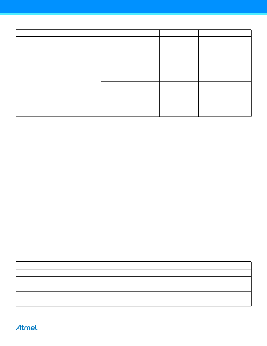
Ordering Information
8.1
ATmega48A
Note:
1. This device can also be supplied in wafer form. Please contact your local Atmel sales office for detailed ordering information
and minimum quantities.
2. Pb-free packaging complies to the European Directive for Restriction of Hazardous Substances (RoHS directive).Also
Halide free and fully Green.
3. See
”Speed Grades” on page 308
.
4. NiPdAu Lead Finish.
5. Tape & Reel.
Speed (MHz)
Power Supply (V)
Ordering Code
(2)
Package
(1)
Operational Range
20
(3)
1.8 - 5.5
ATmega48A-AU
ATmega48A-AUR
(5)
ATmega48A-CCU
ATmega48A-CCUR
(5)
ATmega48A-MMH
(4)
ATmega48A-MMHR
(4)(5)
ATmega48A-MU
ATmega48A-MUR
(5)
ATmega48A-PU
32A
32A
32CC1
32CC1
28M1
28M1
32M1-A
32M1-A
28P3
Industrial
(-40
C to 85
C)
Package Type
32A
32-lead, Thin (1.0 mm) Plastic Quad Flat Package (TQFP)
32CC1
32-ball, 4 x 4 x 0.6 mm package, ball pitch 0.5 mm, Ultra Thin, Fine-Pitch Ball Grill Array (UFBGA)
28M1
28-pad, 4 x 4 x 1.0 body, Lead Pitch 0.45 mm Quad Flat No-Lead/Micro Lead Frame Package (QFN/MLF)
32M1-A
32-pad, 5 x 5 x 1.0 body, Lead Pitch 0.50 mm Quad Flat No-Lead/Micro Lead Frame Package (QFN/MLF)
28P3
28-lead, 0.300” Wide, Plastic Dual Inline Package (PDIP)
13
ATmega48A/PA/88A/PA/168A/PA/328/P [DATASHEET SUMMARY]
8271GS–AVR–02/2013
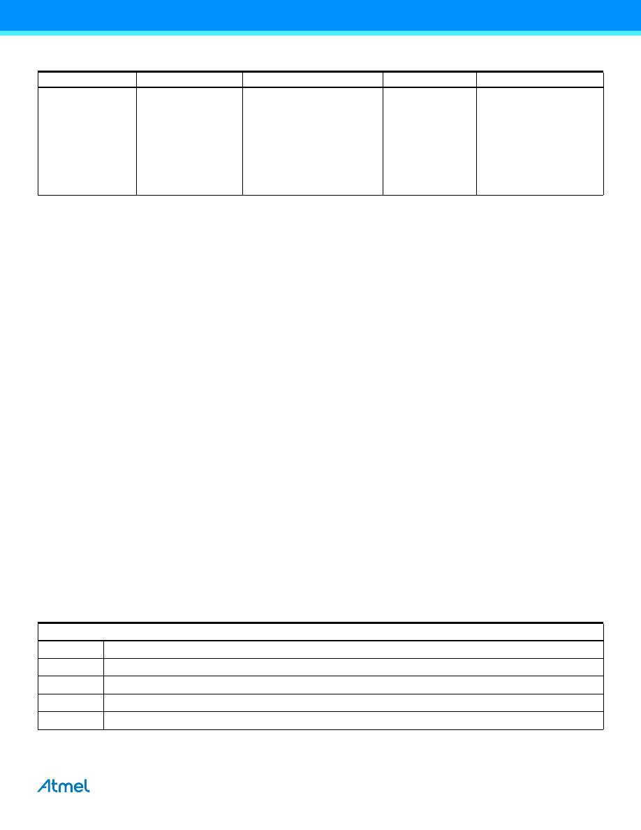
8.2
ATmega48PA
Note:
1. This device can also be supplied in wafer form. Please contact your local Atmel sales office for detailed ordering information
and minimum quantities.
2. Pb-free packaging complies to the European Directive for Restriction of Hazardous Substances (RoHS directive). Also
Halide free and fully Green.
3. See
”Speed Grades” on page 308
.
4. NiPdAu Lead Finish.
5. Tape & Reel.
Speed (MHz)
(3)
Power Supply
Ordering Code
(2)
Package
(1)
Operational Range
20
1.8 - 5.5
ATmega48PA-AU
ATmega48PA-AUR
(5)
ATmega48PA-CCU
ATmega48PA-CCUR
(5)
ATmega48PA-MMH
(4)
ATmega48PA-MMHR
(4)(5)
ATmega48PA-MU
ATmega48PA-MUR
(5)
ATmega48PA-PU
32A
32A
32CC1
32CC1
28M1
28M1
32M1-A
32M1-A
28P3
Industrial
(-40
C to 85
C)
ATmega48PA-AN
ATmega48PA-ANR
(5)
ATmega48PA-MMN
(4)
ATmega48PA-MMNR
(4)(5)
ATmega48PA-MN
ATmega48PA-MNR
(5)
ATmega48PA-PN
32A
32A
28M1
28M1
32M1-A
32M1-A
28P3
Industrial
(-40
C to 105
C)
Package Type
32A
32-lead, Thin (1.0mm) Plastic Quad Flat Package (TQFP)
32CC1
32-ball, 4 x 4 x 0.6mm package, ball pitch 0.5mm, Ultra Thin, Fine-Pitch Ball Grill Array (UFBGA)
28M1
28-pad, 4 x 4 x 1.0 body, Lead Pitch 0.45mm Quad Flat No-Lead/Micro Lead Frame Package (QFN/MLF)
32M1-A
32-pad, 5 x 5 x 1.0 body, Lead Pitch 0.50mm Quad Flat No-Lead/Micro Lead Frame Package (QFN/MLF)
28P3
28-lead, 0.300” Wide, Plastic Dual Inline Package (PDIP)

14
ATmega48A/PA/88A/PA/168A/PA/328/P [DATASHEET SUMMARY]
8271GS–AVR–02/2013
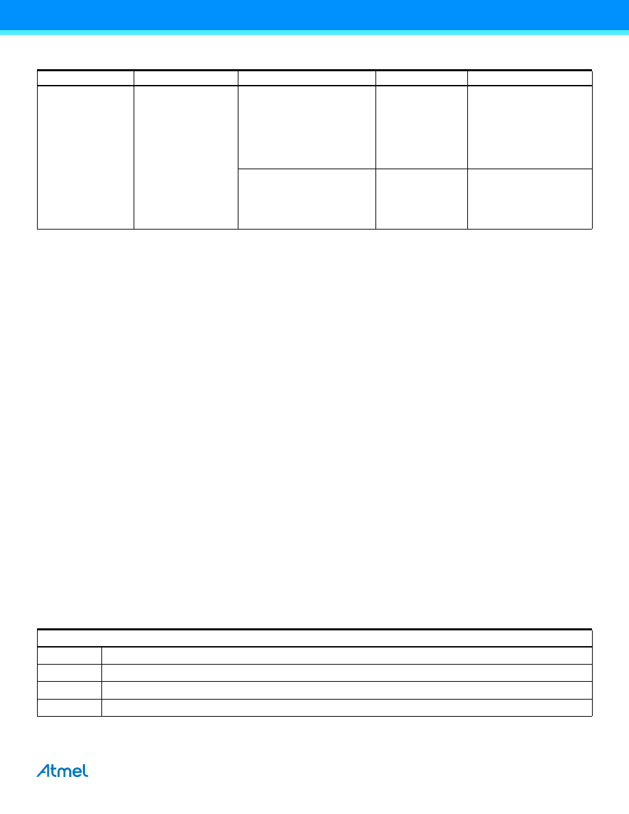
8.3
ATmega88A
Note:
1. This device can also be supplied in wafer form. Please contact your local Atmel sales office for detailed ordering information
and minimum quantities.
2. Pb-free packaging complies to the European Directive for Restriction of Hazardous Substances (RoHS directive).Also
Halide free and fully Green.
3. See
”Speed Grades” on page 308
.
4. NiPdAu Lead Finish.
5. Tape & Reel.
Speed (MHz)
Power Supply (V)
Ordering Code
(2)
Package
(1)
Operational Range
20
(3)
1.8 - 5.5
ATmega88A-AU
ATmega88A-AUR
(5)
ATmega88A-CCU
ATmega88A-CCUR
(5)
ATmega88A-MMH
(4)
ATmega88A-MMHR
(4)(5)
ATmega88A-MU
ATmega88A-MUR
(5)
ATmega88A-PU
32A
32A
32CC1
32CC1
28M1
28M1
32M1-A
32M1-A
28P3
Industrial
(-40
C to 85
C)
Package Type
32A
32-lead, Thin (1.0mm) Plastic Quad Flat Package (TQFP)
32CC1
32-ball, 4 x 4 x 0.6mm package, ball pitch 0.5mm, Ultra Thin, Fine-Pitch Ball Grill Array (UFBGA)
28M1
28-pad, 4 x 4 x 1.0 body, Lead Pitch 0.45mm Quad Flat No-Lead/Micro Lead Frame Package (QFN/MLF)
32M1-A
32-pad, 5 x 5 x 1.0 body, Lead Pitch 0.50mm Quad Flat No-Lead/Micro Lead Frame Package (QFN/MLF)
28P3
28-lead, 0.300” Wide, Plastic Dual Inline Package (PDIP)

15
ATmega48A/PA/88A/PA/168A/PA/328/P [DATASHEET SUMMARY]
8271GS–AVR–02/2013
8.4
ATmega88PA
Note:
1. This device can also be supplied in wafer form. Please contact your local Atmel sales office for detailed ordering information
and minimum quantities.
2. Pb-free packaging complies to the European Directive for Restriction of Hazardous Substances (RoHS directive).Also
Halide free and fully Green.
3. See
”Speed Grades” on page 308
.
4. NiPdAu Lead Finish.
5. Tape & Reel.
Speed (MHz)
(3)
Power Supply (V)
Ordering Code
(2)
Package
(1)
Operational Range
20
1.8 - 5.5
ATmega88PA-AU
ATmega88PA-AUR
(5)
ATmega88PA-CCU
ATmega88PA-CCUR
(5)
ATmega88PA-MMH
(4)
ATmega88PA-MMHR
(4)(5)
ATmega88PA-MU
ATmega88PA-MUR
(5)
ATmega88PA-PU
32A
32A
32CC1
32CC1
28M1
28M1
32M1-A
32M1-A
28P3
Industrial
(-40
C to 85
C)
ATmega88PA-AN
ATmega88PA-ANR
(5)
ATmega88PA-MMN
(4)
ATmega88PA-MMNR
(4)(5)
ATmega88PA-MN
ATmega88PA-MNR
(5)
ATmega88PA-PN
32A
32A
28M1
28M1
32M1-A
32M1-A
28P3
Industrial
(-40
C to 105
C)
Package Type
32A
32-lead, Thin (1.0mm) Plastic Quad Flat Package (TQFP)
32CC1
32-ball, 4 x 4 x 0.6mm package, ball pitch 0.5 mm, Ultra Thin, Fine-Pitch Ball Grill Array (UFBGA)
28M1
28-pad, 4 x 4 x 1.0 body, Lead Pitch 0.45 mm Quad Flat No-Lead/Micro Lead Frame Package (QFN/MLF)
32M1-A
32-pad, 5 x 5 x 1.0 body, Lead Pitch 0.50 mm Quad Flat No-Lead/Micro Lead Frame Package (QFN/MLF)
28P3
28-lead, 0.300” Wide, Plastic Dual Inline Package (PDIP)
16
ATmega48A/PA/88A/PA/168A/PA/328/P [DATASHEET SUMMARY]
8271GS–AVR–02/2013
8.5
ATmega168A
Note:
1. This device can also be supplied in wafer form. Please contact your local Atmel sales office for detailed ordering information
and minimum quantities.
2. Pb-free packaging complies to the European Directive for Restriction of Hazardous Substances (RoHS directive).Also
Halide free and fully Green.
3. See
”Speed Grades” on page 308
4. NiPdAu Lead Finish.
5. Tape & Reel.
Speed (MHz)
(3)
Power Supply (V)
Ordering Code
(2)
Package
(1)
Operational Range
20
1.8 - 5.5
ATmega168A-AU
ATmega168A-AUR
(5)
ATmega168A-CCU
ATmega168A-CCUR
(5)
ATmega168A-MMH
(4)
ATmega168A-MMHR
(4)(5)
ATmega168A-MU
ATmega168A-MUR
(5)
ATmega168A-PU
32A
32A
32CC1
32CC1
28M1
28M1
32M1-A
32M1-A
28P3
Industrial
(-40
C to 85
C)
Package Type
32A
32-lead, Thin (1.0mm) Plastic Quad Flat Package (TQFP)
32CC1
32-ball, 4 x 4 x 0.6 mm package, ball pitch 0.5mm, Ultra Thin, Fine-Pitch Ball Grill Array (UFBGA)
28M1
28-pad, 4 x 4 x 1.0 body, Lead Pitch 0.45mm Quad Flat No-Lead/Micro Lead Frame Package (QFN/MLF)
32M1-A
32-pad, 5 x 5 x 1.0 body, Lead Pitch 0.50mm Quad Flat No-Lead/Micro Lead Frame Package (QFN/MLF)
28P3
28-lead, 0.300” Wide, Plastic Dual Inline Package (PDIP)

17
ATmega48A/PA/88A/PA/168A/PA/328/P [DATASHEET SUMMARY]
8271GS–AVR–02/2013
8.6
ATmega168PA
Note:
1. This device can also be supplied in wafer form. Please contact your local Atmel sales office for detailed ordering information
and minimum quantities.
2. Pb-free packaging complies to the European Directive for Restriction of Hazardous Substances (RoHS directive).Also
Halide free and fully Green.
3. See
”Speed Grades” on page 308
.
4. NiPdAu Lead Finish.
5. Tape & Reel.
Speed (MHz)
(3)
Power Supply (V)
Ordering Code
(2)
Package
(1)
Operational Range
20
1.8 - 5.5
ATmega168PA-AU
ATmega168PA-AUR
(5)
ATmega168PA-CCU
ATmega168PA-CCUR
(5)
ATmega168PA-MMH
(4)
ATmega168PA-MMHR
(4)(5)
ATmega168PA-MU
ATmega168PA-MUR
(5)
ATmega168PA-PU
32A
32A
32CC1
32CC1
28M1
28M1
32M1-A
32M1-A
28P3
Industrial
(-40
C to 85
C)
20
1.8 - 5.5
ATmega168PA-AN
ATmega168PA-ANR
(5)
ATmega168PA-MN
ATmega168PA-MNR
(5)
ATmega168PA-PN
32A
32A
32M1-A
32M1-A
28P3
Industrial
(-40
C to 105
C)
Package Type
32A
32-lead, Thin (1.0mm) Plastic Quad Flat Package (TQFP)
32CC1
32-ball, 4 x 4 x 0.6mm package, ball pitch 0.5mm, Ultra Thin, Fine-Pitch Ball Grill Array (UFBGA)
28M1
28-pad, 4 x 4 x 1.0 body, Lead Pitch 0.45mm Quad Flat No-Lead/Micro Lead Frame Package (QFN/MLF)
32M1-A
32-pad, 5 x 5 x 1.0 body, Lead Pitch 0.50mm Quad Flat No-Lead/Micro Lead Frame Package (QFN/MLF)
28P3
28-lead, 0.300” Wide, Plastic Dual Inline Package (PDIP)

18
ATmega48A/PA/88A/PA/168A/PA/328/P [DATASHEET SUMMARY]
8271GS–AVR–02/2013
8.7
ATmega328
Note:
1. This device can also be supplied in wafer form. Please contact your local Atmel sales office for detailed ordering information
and minimum quantities.
2. Pb-free packaging complies to the European Directive for Restriction of Hazardous Substances (RoHS directive).Also
Halide free and fully Green.
3. See
Figure 29-1 on page 308
.
4. NiPdAu Lead Finish.
5. Tape & Reel
Speed (MHz)
Power Supply (V)
Ordering Code
(2)
Package
(1)
Operational Range
20
(3)
1.8 - 5.5
ATmega328-AU
ATmega328-AUR
(5)
ATmega328-MMH
(4)
ATmega328-MMHR
(4)(5)
ATmega328-MU
ATmega328-MUR
(5)
ATmega328-PU
32A
32A
28M1
28M1
32M1-A
32M1-A
28P3
Industrial
(-40
C to 85
C)
Package Type
32A
32-lead, Thin (1.0mm) Plastic Quad Flat Package (TQFP)
28M1
28-pad, 4 x 4 x 1.0 body, Lead Pitch 0.45mm Quad Flat No-Lead/Micro Lead Frame Package (QFN/MLF)
28P3
28-lead, 0.300” Wide, Plastic Dual Inline Package (PDIP)
32M1-A
32-pad, 5 x 5 x 1.0 body, Lead Pitch 0.50mm Quad Flat No-Lead/Micro Lead Frame Package (QFN/MLF)
19
ATmega48A/PA/88A/PA/168A/PA/328/P [DATASHEET SUMMARY]
8271GS–AVR–02/2013
8.8
ATmega328P
Note:
1. This device can also be supplied in wafer form. Please contact your local Atmel sales office for detailed ordering information
and minimum quantities.
2. Pb-free packaging complies to the European Directive for Restriction of Hazardous Substances (RoHS directive).Also
Halide free and fully Green.
3. See
Figure 29-1 on page 308
.
4. NiPdAu Lead Finish.
5. Tape & Reel.
Speed (MHz)
(3)
Power Supply (V)
Ordering Code
(2)
Package
(1)
Operational Range
20
1.8 - 5.5
ATmega328P-AU
ATmega328P-AUR
(5)
ATmega328P-MMH
(4)
ATmega328P-MMHR
(4)(5)
ATmega328P-MU
ATmega328P-MUR
(5)
ATmega328P-PU
32A
32A
28M1
28M1
32M1-A
32M1-A
28P3
Industrial
(-40
C to 85
C)
ATmega328P-AN
ATmega328P-ANR
(5)
ATmega328P-MN
ATmega328P-MNR
(5)
ATmega328P-PN
32A
32A
32M1-A
32M1-A
28P3
Industrial
(-40
C to 105
C)
Package Type
32A
32-lead, Thin (1.0mm) Plastic Quad Flat Package (TQFP)
28M1
28-pad, 4 x 4 x 1.0 body, Lead Pitch 0.45mm Quad Flat No-Lead/Micro Lead Frame Package (QFN/MLF)
28P3
28-lead, 0.300” Wide, Plastic Dual Inline Package (PDIP)
32M1-A
32-pad, 5 x 5 x 1.0 body, Lead Pitch 0.50mm Quad Flat No-Lead/Micro Lead Frame Package (QFN/MLF)
20
ATmega48A/PA/88A/PA/168A/PA/328/P [DATASHEET SUMMARY]
8271GS–AVR–02/2013
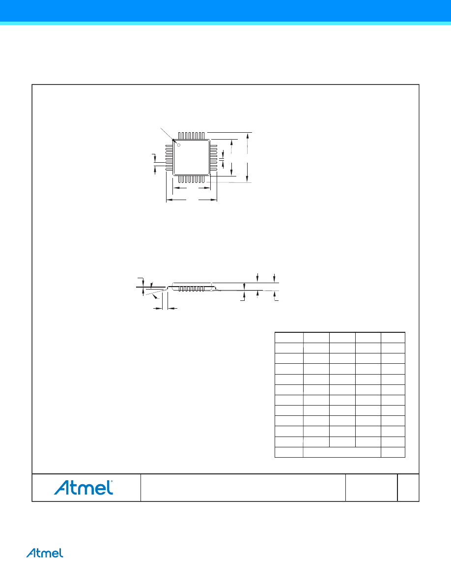
9.
Packaging Information
9.1
32A
TITLE
DRAWING NO.
REV.
32A, 32-lead, 7 x 7mm body size, 1.0mm body thickness,
0.8mm lead pitch, thin profile plastic quad flat package (TQFP)
C
32A
2010-10-20
PIN 1 IDENTIFIER
0°~7°
PIN 1
L
C
A1
A2
A
D1
D
e
E1
E
B
Notes:
1. This package conforms to JEDEC reference MS-026, Variation ABA.
2. Dimensions D1 and E1 do not include mold protrusion.
Allowable
protrusion is 0.25mm per side. Dimensions D1 and E1 are maximum
plastic body size dimensions including mold mismatch.
3. Lead coplanarity is 0.10mm maximum.
A
–
–
1.20
A1
0.05
–
0.15
A2
0.95
1.00
1.05
D
8.75
9.00
9.25
D1
6.90
7.00
7.10
Note 2
E
8.75
9.00
9.25
E1
6.90
7.00
7.10
Note 2
B 0.30
–
0.45
C
0.09
–
0.20
L
0.45
–
0.75
e
0.80 TYP
COMMON DIMENSIONS
(Unit of measure = mm)
SYMBOL
MIN
NOM
MAX
NOTE
21
ATmega48A/PA/88A/PA/168A/PA/328/P [DATASHEET SUMMARY]
8271GS–AVR–02/2013
9.2
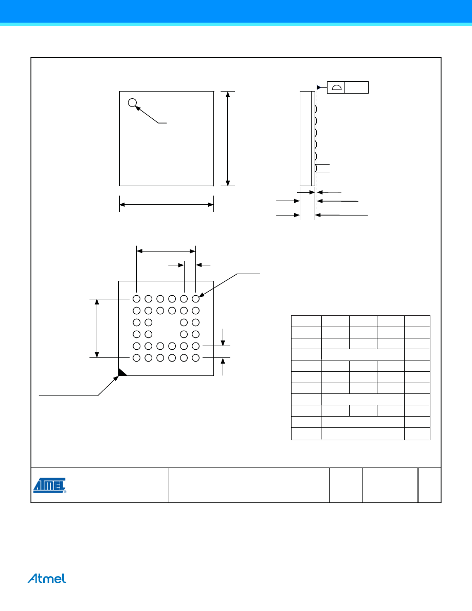
32CC1
TITLE
DRAWING NO.
GPC
REV.
Package Drawing Contact:
packagedrawings@atmel.com
B
CAG
32CC1, 32-ball (6 x 6 Array), 4 x 4 x 0.6 mm
package, ball pitch 0.50 mm, Ultra Thin,
Fine-Pitch Ball Grid Array (UFBGA)
32CC1
A – –
0.60
A1 0.12 – –
A2 0.38 REF
b 0.25
0.30
0.35
1
b1 0.25 – – 2
D 3.90
4.00
4.10
D1
2.50 BSC
E 3.90
4.00
4.10
E1
2.50 BSC
e
0.50 BSC
07/06/10
b1
COMMON DIMENSIONS
(Unit of Measure = mm)
1 2
3
4
5
6
B
A
C
D
E
F
E
D
e
32-Øb
E
D
B
A
Pin#1 ID
0.08
A1
A
D1
E1
A2
A1 BALL CORNER
1 2
3
4
5
6
F
C
SIDE VIEW
BOTTOM VIEW
TOP VIEW
SYMBOL
MIN
NOM
MAX
NOTE
Note1:
Dimension “b” is measured at the maximum ball dia. in a plane parallel
to the seating plane.
Note2:
Dimension “b1” is the solderable surface defined by the opening of the
solder resist layer.
e
22
ATmega48A/PA/88A/PA/168A/PA/328/P [DATASHEET SUMMARY]
8271GS–AVR–02/2013
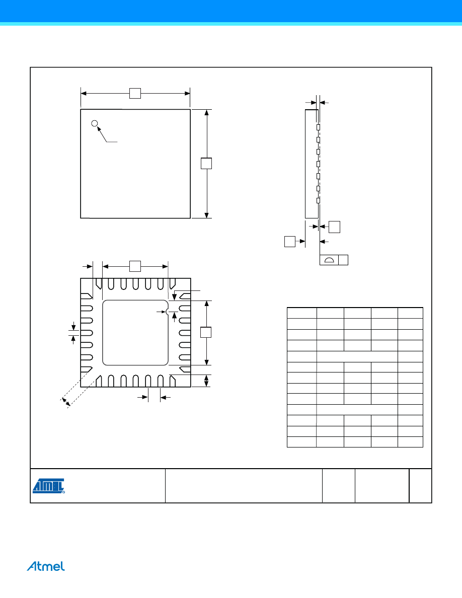
9.3
28M1
TITLE
DRAWING NO.
GPC
REV.
Package Drawing Contact:
packagedrawings@atmel.com
28M1
ZBV
B
28M1, 28-pad, 4 x 4 x 1.0mm Body, Lead Pitch 0.45mm,
2.4 x 2.4mm Exposed Pad, Thermally Enhanced
Plastic Very Thin Quad Flat No Lead Package (VQFN)
10/24/08
SIDE VIEW
Pin 1 ID
BOTTOM VIEW
TOP VIEW
Note: The terminal #1 ID is a Laser-marked Feature.
D
E
e
K
A1
C
A
D2
E2
y
L
1
2
3
b
1
2
3
0.45
COMMON DIMENSIONS
(Unit of Measure = mm)
SYMBOL
MIN
NOM
MAX
NOTE
A
0.80 0.90 1.00
A1
0.00 0.02 0.05
b
0.17
0.22
0.27
C
0.20 REF
D
3.95
4.00
4.05
D2
2.35
2.40
2.45
E
3.95
4.00
4.05
E2
2.35
2.40
2.45
e
0.45
L
0.35
0.40
0.45
y
0.00
–
0.08
K
0.20
– –
R 0.20
0.4 Ref
(4x)
23
ATmega48A/PA/88A/PA/168A/PA/328/P [DATASHEET SUMMARY]
8271GS–AVR–02/2013
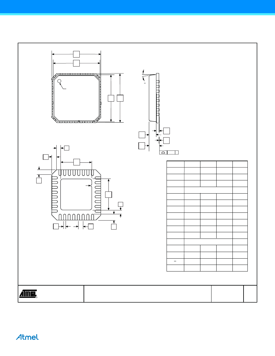
9.4
32M1-A
2325 Orchard Parkway
San Jose, CA 95131
TITLE
DRAWING NO.
R
REV.
32M1-A, 32-pad, 5 x 5 x 1.0mm Body, Lead Pitch 0.50mm,
E
32M1-A
5/25/06
3.10mm Exposed Pad, Micro Lead Frame Package (MLF)
COMMON DIMENSIONS
(Unit of Measure = mm)
SYMBOL
MIN
NOM
MAX
NOTE
D1
D
E1
E
e
b
A3
A2
A1
A
D2
E2
0.08 C
L
1
2
3
P
P
0
1
2
3
A
0.80
0.90
1.00
A1
–
0.02
0.05
A2
–
0.65
1.00
A3
0.20 REF
b
0.18
0.23
0.30
D
D1
D2
2.95
3.10
3.25
4.90
5.00
5.10
4.70
4.75
4.80
4.70
4.75
4.80
4.90
5.00
5.10
E
E1
E2
2.95
3.10
3.25
e
0.50 BSC
L
0.30
0.40
0.50
P
–
–
0.60
–
–
12
o
Note: JEDEC Standard MO-220, Fig. 2 (Anvil Singulation), VHHD-2.
TOP VIEW
SIDE VIEW
BOTTOM VIEW
0
Pin 1 ID
Pin #1 Notch
(0.20 R)
K
0.20
–
–
K
K
24
ATmega48A/PA/88A/PA/168A/PA/328/P [DATASHEET SUMMARY]
8271GS–AVR–02/2013
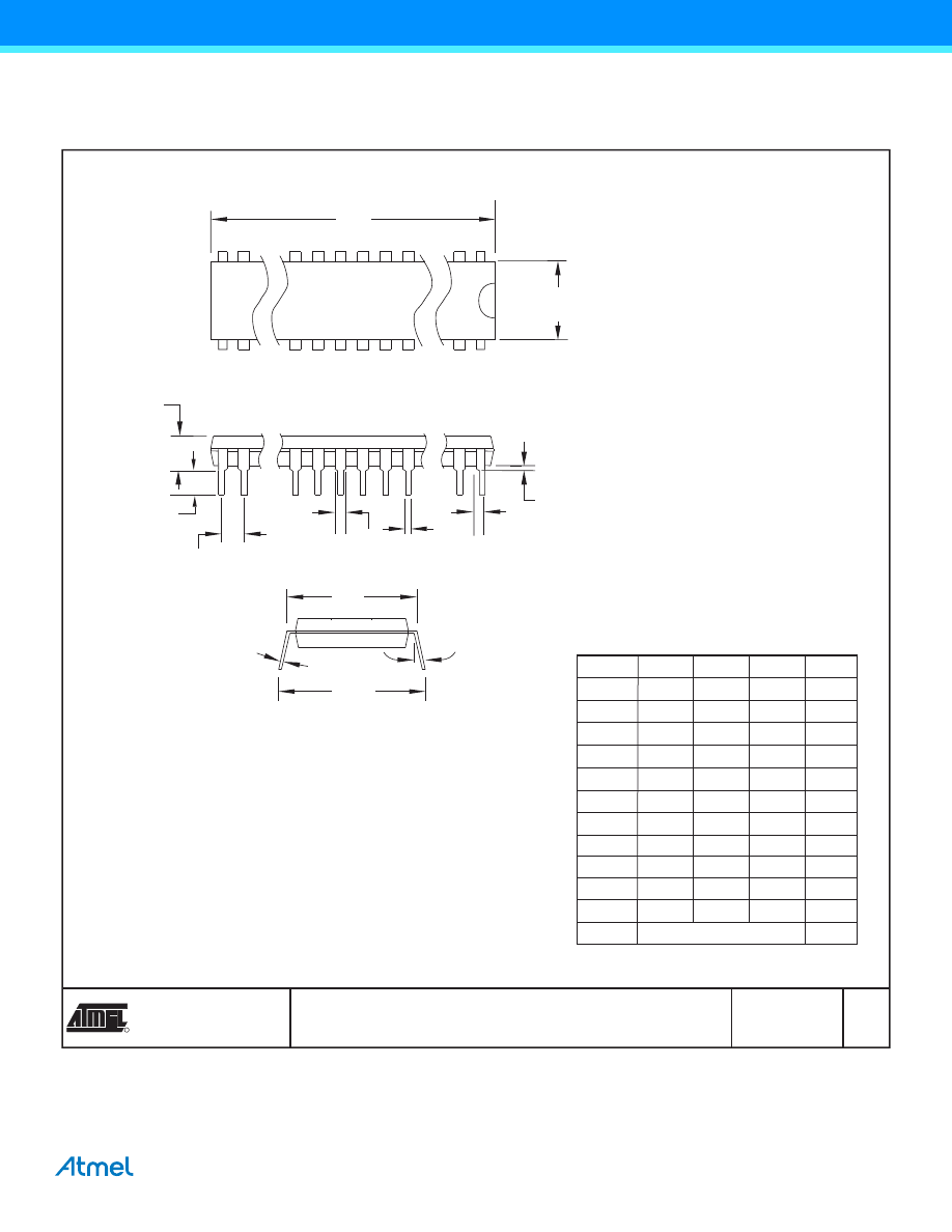
9.5
28P3
2325 Orchard Parkway
San Jose, CA 95131
TITLE
DRAWING NO.
R
REV.
28P3, 28-lead (0.300"/7.62mm Wide) Plastic Dual
Inline Package (PDIP)
B
28P3
09/28/01
PIN
1
E1
A1
B
REF
E
B1
C
L
SEATING PLANE
A
0º ~ 15º
D
e
eB
B2
(4 PLACES)
COMMON DIMENSIONS
(Unit of Measure = mm)
SYMBOL
MIN
NOM
MAX
NOTE
A
–
–
4.5724
A1
0.508
–
–
D
34.544
–
34.798 Note 1
E
7.620
–
8.255
E1
7.112
–
7.493
Note 1
B
0.381
–
0.533
B1
1.143
–
1.397
B2
0.762
–
1.143
L
3.175
–
3.429
C
0.203
–
0.356
eB
–
–
10.160
e 2.540 TYP
Note:
1. Dimensions D and E1 do not include mold Flash or Protrusion.
Mold Flash or Protrusion shall not exceed 0.25mm (0.010").

25
ATmega48A/PA/88A/PA/168A/PA/328/P [DATASHEET SUMMARY]
8271GS–AVR–02/2013
10. Errata
10.1
Errata ATmega48A
The revision letter in this section refers to the revision of the ATmega48A device.
10.1.1
Rev. D
•
Analog MUX can be turned off when setting ACME bit
•
TWI Data setup time can be too short
1.
Analog MUX can be turned off when setting ACME bit
If the ACME (Analog Comparator Multiplexer Enabled) bit in ADCSRB is set while MUX3 in ADMUX is '1'
(ADMUX[3:0]=1xxx), all MUX'es are turned off until the ACME bit is cleared.
Problem Fix/Workaround
Clear the MUX3 bit before setting the ACME bit.
2.
TWI Data setup time can be too short
When running the device as a TWI slave with a system clock above 2MHz, the data setup time for the first bit
after ACK may in some cases be too short. This may cause a false start or stop condition on the TWI line.
Problem Fix/Workaround
Insert a delay between setting TWDR and TWCR.
10.2
Errata ATmega48PA
The revision letter in this section refers to the revision of the ATmega48PA device.
10.2.1
Rev. D
•
Analog MUX can be turned off when setting ACME bit
•
TWI Data setup time can be too short
1.
Analog MUX can be turned off when setting ACME bit
If the ACME (Analog Comparator Multiplexer Enabled) bit in ADCSRB is set while MUX3 in ADMUX is '1'
(ADMUX[3:0]=1xxx), all MUX'es are turned off until the ACME bit is cleared.
Problem Fix/Workaround
Clear the MUX3 bit before setting the ACME bit.
2.
TWI Data setup time can be too short
When running the device as a TWI slave with a system clock above 2MHz, the data setup time for the first bit
after ACK may in some cases be too short. This may cause a false start or stop condition on the TWI line.
Problem Fix/Workaround
Insert a delay between setting TWDR and TWCR.

26
ATmega48A/PA/88A/PA/168A/PA/328/P [DATASHEET SUMMARY]
8271GS–AVR–02/2013
10.3
Errata ATmega88A
The revision letter in this section refers to the revision of the ATmega88A device.
10.3.1
Rev. F
•
Analog MUX can be turned off when setting ACME bit
•
TWI Data setup time can be too short
1.
Analog MUX can be turned off when setting ACME bit
If the ACME (Analog Comparator Multiplexer Enabled) bit in ADCSRB is set while MUX3 in ADMUX is '1'
(ADMUX[3:0]=1xxx), all MUX'es are turned off until the ACME bit is cleared.
Problem Fix/Workaround
Clear the MUX3 bit before setting the ACME bit.
2.
TWI Data setup time can be too short
When running the device as a TWI slave with a system clock above 2MHz, the data setup time for the first bit
after ACK may in some cases be too short. This may cause a false start or stop condition on the TWI line.
Problem Fix/Workaround
Insert a delay between setting TWDR and TWCR.
10.4
Errata ATmega88PA
The revision letter in this section refers to the revision of the ATmega88PA device.
10.4.1
Rev. F
•
Analog MUX can be turned off when setting ACME bit
•
TWI Data setup time can be too short
1.
Analog MUX can be turned off when setting ACME bit
If the ACME (Analog Comparator Multiplexer Enabled) bit in ADCSRB is set while MUX3 in ADMUX is '1'
(ADMUX[3:0]=1xxx), all MUX'es are turned off until the ACME bit is cleared.
Problem Fix/Workaround
Clear the MUX3 bit before setting the ACME bit.
2.
TWI Data setup time can be too short
When running the device as a TWI slave with a system clock above 2MHz, the data setup time for the first bit
after ACK may in some cases be too short. This may cause a false start or stop condition on the TWI line.
Problem Fix/Workaround
Insert a delay between setting TWDR and TWCR.

27
ATmega48A/PA/88A/PA/168A/PA/328/P [DATASHEET SUMMARY]
8271GS–AVR–02/2013
10.5
Errata ATmega168A
The revision letter in this section refers to the revision of the ATmega168A device.
10.5.1
Rev. E
•
Analog MUX can be turned off when setting ACME bit
•
TWI Data setup time can be too short
1.
Analog MUX can be turned off when setting ACME bit
If the ACME (Analog Comparator Multiplexer Enabled) bit in ADCSRB is set while MUX3 in ADMUX is '1'
(ADMUX[3:0]=1xxx), all MUX'es are turned off until the ACME bit is cleared.
Problem Fix/Workaround
Clear the MUX3 bit before setting the ACME bit.
2.
TWI Data setup time can be too short
When running the device as a TWI slave with a system clock above 2MHz, the data setup time for the first bit
after ACK may in some cases be too short. This may cause a false start or stop condition on the TWI line.
Problem Fix/Workaround
Insert a delay between setting TWDR and TWCR.
10.6
Errata ATmega168PA
The revision letter in this section refers to the revision of the ATmega168PA device.
10.6.1
Rev E
•
Analog MUX can be turned off when setting ACME bit
•
TWI Data setup time can be too short
1.
Analog MUX can be turned off when setting ACME bit
If the ACME (Analog Comparator Multiplexer Enabled) bit in ADCSRB is set while MUX3 in ADMUX is '1'
(ADMUX[3:0]=1xxx), all MUX'es are turned off until the ACME bit is cleared.
Problem Fix/Workaround
Clear the MUX3 bit before setting the ACME bit.
2.
TWI Data setup time can be too short
When running the device as a TWI slave with a system clock above 2MHz, the data setup time for the first bit
after ACK may in some cases be too short. This may cause a false start or stop condition on the TWI line.
Problem Fix/Workaround
Insert a delay between setting TWDR and TWCR.

28
ATmega48A/PA/88A/PA/168A/PA/328/P [DATASHEET SUMMARY]
8271GS–AVR–02/2013
10.7
Errata ATmega328
The revision letter in this section refers to the revision of the ATmega328 device.
10.7.1
Rev D
•
Analog MUX can be turned off when setting ACME bit
•
TWI Data setup time can be too short
1.
Analog MUX can be turned off when setting ACME bit
If the ACME (Analog Comparator Multiplexer Enabled) bit in ADCSRB is set while MUX3 in ADMUX is '1'
(ADMUX[3:0]=1xxx), all MUX'es are turned off until the ACME bit is cleared.
Problem Fix/Workaround
Clear the MUX3 bit before setting the ACME bit.
2.
TWI Data setup time can be too short
When running the device as a TWI slave with a system clock above 2MHz, the data setup time for the first bit
after ACK may in some cases be too short. This may cause a false start or stop condition on the TWI line.
Problem Fix/Workaround
Insert a delay between setting TWDR and TWCR.
10.7.2
Rev C
Not sampled.
10.7.3
Rev B
•
Analog MUX can be turned off when setting ACME bit
•
Unstable 32kHz Oscillator
1.
Analog MUX can be turned off when setting ACME bit
If the ACME (Analog Comparator Multiplexer Enabled) bit in ADCSRB is set while MUX3 in ADMUX is '1'
(ADMUX[3:0]=1xxx), all MUX'es are turned off until the ACME bit is cleared.
Problem Fix/Workaround
Clear the MUX3 bit before setting the ACME bit.
2.
Unstable 32kHz Oscillator
The 32kHz oscillator does not work as system clock. The 32kHz oscillator used as asynchronous timer is
inaccurate.
Problem Fix/ Workaround
None.
10.7.4
Rev A
•
Analog MUX can be turned off when setting ACME bit
•
Unstable 32kHz Oscillator
1.
Analog MUX can be turned off when setting ACME bit
If the ACME (Analog Comparator Multiplexer Enabled) bit in ADCSRB is set while MUX3 in ADMUX is '1'
(ADMUX[3:0]=1xxx), all MUX'es are turned off until the ACME bit is cleared.
Problem Fix/Workaround
Clear the MUX3 bit before setting the ACME bit.

29
ATmega48A/PA/88A/PA/168A/PA/328/P [DATASHEET SUMMARY]
8271GS–AVR–02/2013
2.
Unstable 32kHz Oscillator
The 32kHz oscillator does not work as system clock. The 32kHz oscillator used as asynchronous timer is
inaccurate.
Problem Fix/ Workaround
None.
10.8
Errata ATmega328P
The revision letter in this section refers to the revision of the ATmega328P device.
10.8.1
Rev D
•
Analog MUX can be turned off when setting ACME bit
•
TWI Data setup time can be too short
1.
Analog MUX can be turned off when setting ACME bit
If the ACME (Analog Comparator Multiplexer Enabled) bit in ADCSRB is set while MUX3 in ADMUX is '1'
(ADMUX[3:0]=1xxx), all MUX'es are turned off until the ACME bit is cleared.
Problem Fix/Workaround
Clear the MUX3 bit before setting the ACME bit.
2.
TWI Data setup time can be too short
When running the device as a TWI slave with a system clock above 2MHz, the data setup time for the first bit
after ACK may in some cases be too short. This may cause a false start or stop condition on the TWI line.
Problem Fix/Workaround
Insert a delay between setting TWDR and TWCR.
10.8.2
Rev C
Not sampled.
10.8.3
Rev B
•
Analog MUX can be turned off when setting ACME bit
•
Unstable 32kHz Oscillator
1.
Analog MUX can be turned off when setting ACME bit
If the ACME (Analog Comparator Multiplexer Enabled) bit in ADCSRB is set while MUX3 in ADMUX is '1'
(ADMUX[3:0]=1xxx), all MUX'es are turned off until the ACME bit is cleared.
Problem Fix/Workaround
Clear the MUX3 bit before setting the ACME bit.
2.
Unstable 32kHz Oscillator
The 32kHz oscillator does not work as system clock. The 32kHz oscillator used as asynchronous timer is
inaccurate.
Problem Fix/ Workaround
None.

30
ATmega48A/PA/88A/PA/168A/PA/328/P [DATASHEET SUMMARY]
8271GS–AVR–02/2013
10.8.4
Rev A
•
Unstable 32kHz Oscillator
1.
Unstable 32kHz Oscillator
The 32kHz oscillator does not work as system clock. The 32kHz oscillator used as asynchronous timer is
inaccurate.
Problem Fix/ Workaround
None.

Atmel Corporation
1600 Technology Drive
San Jose, CA 95110
USA
Tel: (+1) (408) 441-0311
Fax: (+1) (408) 487-2600
www.atmel.com
Atmel Asia Limited
Unit 01-5 & 16, 19F
BEA Tower, Millennium City 5
418 Kwun Tong Roa
Kwun Tong, Kowloon
HONG KONG
Tel: (+852) 2245-6100
Fax: (+852) 2722-1369
Atmel Munich GmbH
Business Campus
Parkring 4
D-85748 Garching b. Munich
GERMANY
Tel: (+49) 89-31970-0
Fax: (+49) 89-3194621
Atmel Japan G.K.
16F Shin-Osaki Kangyo Bldg
1-6-4 Osaki, Shinagawa-ku
Tokyo 141-0032
JAPAN
Tel: (+81) (3) 6417-0300
Fax: (+81) (3) 6417-0370
© 2013 Atmel Corporation. All rights reserved. / Rev.: 8271GS–AVR–02/2013
Disclaimer: The information in this document is provided in connection with Atmel products. No license, express or implied, by estoppel or otherwise, to any intellectual property right is granted by this
document or in connection with the sale of Atmel products. EXCEPT AS SET FORTH IN THE ATMEL TERMS AND CONDITIONS OF SALES LOCATED ON THE ATMEL WEBSITE, ATMEL ASSUMES
NO LIABILITY WHATSOEVER AND DISCLAIMS ANY EXPRESS, IMPLIED OR STATUTORY WARRANTY RELATING TO ITS PRODUCTS INCLUDING, BUT NOT LIMITED TO, THE IMPLIED
WARRANTY OF MERCHANTABILITY, FITNESS FOR A PARTICULAR PURPOSE, OR NON-INFRINGEMENT. IN NO EVENT SHALL ATMEL BE LIABLE FOR ANY DIRECT, INDIRECT,
CONSEQUENTIAL, PUNITIVE, SPECIAL OR INCIDENTAL DAMAGES (INCLUDING, WITHOUT LIMITATION, DAMAGES FOR LOSS AND PROFITS, BUSINESS INTERRUPTION, OR LOSS OF
INFORMATION) ARISING OUT OF THE USE OR INABILITY TO USE THIS DOCUMENT, EVEN IF ATMEL HAS BEEN ADVISED OF THE POSSIBILITY OF SUCH DAMAGES. Atmel makes no
representations or warranties with respect to the accuracy or completeness of the contents of this document and reserves the right to make changes to specifications and products descriptions at any time
without notice. Atmel does not make any commitment to update the information contained herein. Unless specifically provided otherwise, Atmel products are not suitable for, and shall not be used in,
automotive applications. Atmel products are not intended, authorized, or warranted for use as components in applications intended to support or sustain life.
Atmel
®
, Atmel logo and combinations thereof, Enabling Unlimited Possibilities
®
, and others are registered trademarks or trademarks of Atmel Corporation or its
subsidiaries. Other terms and product names may be trademarks of others.
Document Outline
- Features
- 1. Pin Configurations
- 2. Overview
- 3. Resources
- 4. Data Retention
- 5. About Code Examples
- 6. Capacitive Touch Sensing
- 7. Register Summary
- 8. Ordering Information
- 9. Packaging Information
- 10. Errata
Wyszukiwarka
Podobne podstrony:
Atmel Avr USB Software Library for AT90USBxxx Microcontrollers doc7675
AT89C51 8 bit Microcontroller with 4K Bytes Flash
Atmel Avr USB Firmware Upgrade For AT90USB doc7769
Atmel AVR Assembler id 71678 Nieznany (2)
ATMEGA64L8AU ATMEL id 71661 Nieznany (2)
8 Bit Microcontroller Drives Ba Nieznany (2)
(dsp digitalfilter) atmel digital filters with avr
Atmel Avr Efficient C Coding
Atmel Avr Self Programming
AT89C51 8 bit Microcontroller with 4K Bytes Flash
Atmel Avr USB Firmware Upgrade For AT90USB doc7769
Atmel AVR Assembler id 71678 Nieznany (2)
A digital thermometer or talk I2C to your atmel microcontroller
więcej podobnych podstron