BYW32...BYW36
Vishay Telefunken
www.vishay.de
•
FaxBack +1-408-970-5600
Rev. 2, 24-Jun-98
1 (4)
Document Number 86048
Fast Silicon Mesa Rectifiers
Features
D
Glass passivated junction
D
Hermetically sealed package
D
Low reverse current
D
Soft recovery characteristics
Applications
Fast rectifier and switch for example for TV–line output
circuits and switch mode power supply
94 9539
Absolute Maximum Ratings
T
j
= 25
_
C
Parameter
Test Conditions
Type
Symbol
Value
Unit
Reverse voltage
BYW32
V
R
=V
RRM
200
V
g
=Repetitive peak reverse voltage
BYW33
V
R
=V
RRM
300
V
BYW34
V
R
=V
RRM
400
V
BYW35
V
R
=V
RRM
500
V
BYW36
V
R
=V
RRM
600
V
Peak forward surge current
t
p
=10ms,
half sinewave
I
FSM
50
A
Repetitive peak forward current
I
FRM
12
A
Average forward current
ϕ
=180
°
I
FAV
2
A
Junction and storage temperature range
T
j
=T
stg
–55...+175
°
C
Maximum Thermal Resistance
T
j
= 25
_
C
Parameter
Test Conditions
Symbol
Value
Unit
Junction ambient
l=10mm, T
L
=constant
R
thJA
45
K/W
on PC board with spacing 25mm
R
thJA
100
K/W
Electrical Characteristics
T
j
= 25
_
C
Parameter
Test Conditions
Type
Symbol
Min
Typ
Max
Unit
Forward voltage
I
F
=1A
V
F
0.95
1.1
V
Reverse current
V
R
=V
RRM
I
R
1
5
m
A
V
R
=V
RRM
, T
j
=150
°
C
I
R
60
150
m
A
Reverse recovery time
I
F
=0.5A, I
R
=1A, i
R
=0.25A
t
rr
200
ns
BYW32...BYW36
Vishay Telefunken
www.vishay.de
•
FaxBack +1-408-970-5600
Rev. 2, 24-Jun-98
2 (4)
Document Number 86048
Characteristics (T
j
= 25
_
C unless otherwise specified)
0
0
20
40
60
80
120
R –
Therm. Resist. Junction /
Ambient ( K/W
)
thJA
l – Lead Length ( mm )
94 9552
5
10
15
25
30
20
100
l
l
T
L
=constant
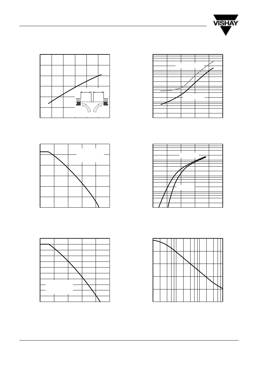
Figure 1. Max. Thermal Resistance vs. Lead Length
0
40
80
120
160
0
0.2
0.4
0.6
0.8
1.2
I –
A
verage
Forward
Current
(
A
)
FA
V
T
amb
– Ambient Temperature (
°
C )
200
94 9558
1.0
R
thJA
=100K/W
f
v20kHz
PC Board
Figure 2. Max. Average Forward Current vs.
Ambient Temperature
0
0
0.4
0.8
1.2
1.6
2.0
I –
A
verage
Forward
Current
(
A
)
FA
V
T
amb
– Ambient Temperature (
°
C )
94 9559
40
80
120
160
200
f
v20kHz
R
thJA
=45K/W
l=10mm
Figure 3. Max. Average Forward Current vs.
Ambient Temperature
0
40
80
120
160
0.1
1
10
100
1000
T
j
– Junction Temperature (
°
C )
200
94 9560
m
I – Reverse Current (
A
)
R
Scattering Limit
V
R
= V
R RM
Figure 4. Reverse Current vs. Junction Temperature
0
0.6
1.2
1.8
2.4
0.01
0.1
1
10
100
I – Forward Current (
A
)
F
V
F
– Forward Voltage ( V )
3.0
94 9555
T
j
= 25
°
C
T
j
= 175
°
C
Figure 5. Max. Forward Current vs. Forward Voltage
0
4
8
12
16
20
0.1
1
10
C – Diode Capacitance ( pF )
D
V
R
– Reverse Voltage ( V )
100
94 9557
Figure 6. Typ. Diode Capacitance vs. Reverse Voltage
BYW32...BYW36
Vishay Telefunken
www.vishay.de
•
FaxBack +1-408-970-5600
Rev. 2, 24-Jun-98
3 (4)
Document Number 86048
1
10
100
1000
Z –
Thermal Resistance for Pulse Cond. (K/W)
thp
t
p
– Pulse Length ( s )
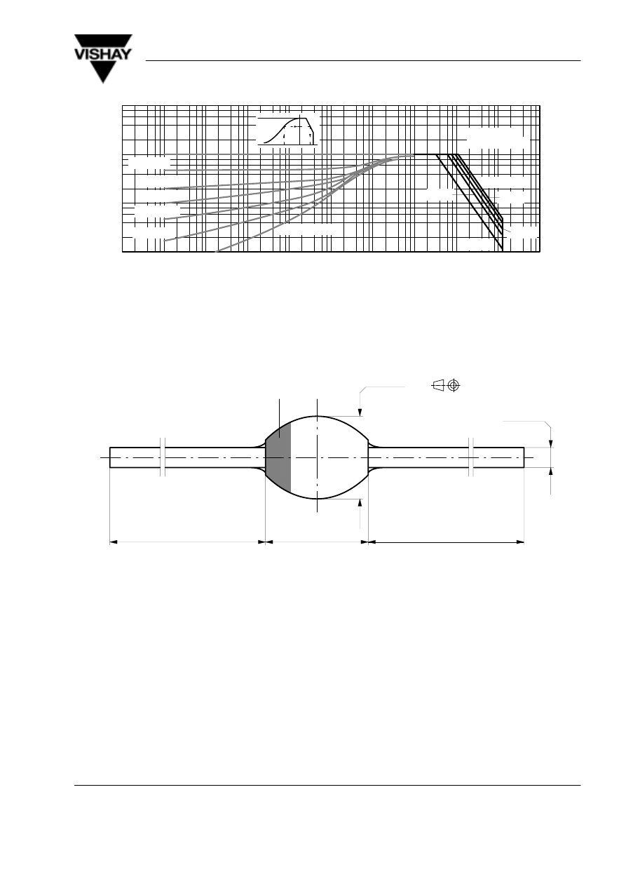
94 9561
10
–5
10
–4
10
–3
10
–2
10
–1
10
0
10
1
I
FRM
– Repetitive Peak
Forward Current ( A )
10
0
10
1
V
R RM
=600V
R
thJA
=100K/W
t
p
/T=0.5
t
p
/T=0.2
t
p
/T=0.1
t
p
/T=0.02
t
p
/T=0.01
T
amb
= 25
°
C
45
°
C
50
°
C
70
°
C
100
°
C
Single pulse
Figure 7. Thermal Response
Dimensions in mm
Cathode Identification
∅
3.6 max.
∅
0.82 max.
4.2 max.
Sintered Glass Case
SOD 57
Weight max. 0.5 g
technical drawings
according to DIN
specifications
94 9538
26 min.
26 min.

BYW32...BYW36
Vishay Telefunken
www.vishay.de
•
FaxBack +1-408-970-5600
Rev. 2, 24-Jun-98
4 (4)
Document Number 86048
Ozone Depleting Substances Policy Statement
It is the policy of Vishay Semiconductor GmbH to
1. Meet all present and future national and international statutory requirements.
2. Regularly and continuously improve the performance of our products, processes, distribution and operating
systems
with respect to their impact on the health and safety of our employees and the public, as well as their impact on
the environment.
It is particular concern to control or eliminate releases of those substances into the atmosphere which are known as
ozone depleting substances ( ODSs ).
The Montreal Protocol ( 1987 ) and its London Amendments ( 1990 ) intend to severely restrict the use of ODSs and
forbid their use within the next ten years. Various national and international initiatives are pressing for an earlier ban
on these substances.
Vishay Semiconductor GmbH has been able to use its policy of continuous improvements to eliminate the use of
ODSs listed in the following documents.
1. Annex A, B and list of transitional substances of the Montreal Protocol and the London Amendments respectively
2 . Class I and II ozone depleting substances in the Clean Air Act Amendments of 1990 by the Environmental
Protection Agency ( EPA ) in the USA
3. Council Decision 88/540/EEC and 91/690/EEC Annex A, B and C ( transitional substances ) respectively.
Vishay Semiconductor GmbH can certify that our semiconductors are not manufactured with ozone depleting
substances and do not contain such substances.
We reserve the right to make changes to improve technical design and may do so without further notice.
Parameters can vary in different applications. All operating parameters must be validated for each customer application
by the customer. Should the buyer use Vishay-Telefunken products for any unintended or unauthorized application, the
buyer shall indemnify Vishay-Telefunken against all claims, costs, damages, and expenses, arising out of, directly or
indirectly, any claim of personal damage, injury or death associated with such unintended or unauthorized use.
Vishay Semiconductor GmbH, P.O.B. 3535, D-74025 Heilbronn, Germany
Telephone: 49 ( 0 ) 7131 67 2831, Fax number: 49 ( 0 ) 7131 67 2423
Wyszukiwarka
Podobne podstrony:
odp na 33 34 35, mgr inż
33, 34, 35 korekcyjna
OBSERWACJA nr3 34 35 36 siatka
34,35,36 id 35887 Nieznany (2)
32 33 34 35 wielki format
20,21,22,23,24,25,26,27,28,29,30,31,32,33,34,35 opracowane pytania egzamin historia wychowania
34, 35, 36
31, 32, 33, 34, 36, 37, 38, 39
33 34
34 35
34 35 id 35922 Nieznany
34 35 Лазеры, квантово механ методы
35,36
35 36
ei 03 2002 s 34 35
33 34
fiszki 01 33 i 34
więcej podobnych podstron