
Analog Integrated Circuits and Signal Processing, 32, 37–46, 2002
C
2002 Kluwer Academic Publishers. Manufactured in The Netherlands.
Simulations Based Design for a Large Displacement Electrostatically
Actuated Microrelay
GOOI BOON CHONG,
1
KAM SEE HOON,
1
IJAZ H. JAFRI
2
∗
AND DANIEL J. KEATING
2
1
Nanyang Polytechnic School of Engineering, 80 Ang Mo Kio Ave 8, Singapore 569830
2
Corning Intellisense, 36 Jonspin Road, Wilmington, MA 01887, USA Tel.: +1 (978)988-8000, Fax: +1 (978)988-8001
E-mail: GOOI Boon Chong@nyp.gov.sg; KAM See Hoon@nyp.gov.sg; JafriIH@corning.com; KeatingDJ@corning.com
Received May 18, 2001; Accepted September 14, 2001
Abstract. An electrostatically actuated microrelay with large displacement, small actuation voltage and limited
plate surface dimensions is designed to meet stringent telecommunication switching requirements. Fabrication
feasibility and performance characteristics of the device are evaluated using a commercial CAD for MEMS tool.
Simulation results of the device performance including pull-in voltages for different suspension stiffness variations,
natural frequencies, stresses and restoring forces are presented.
Key Words: microrelay, microswitch, electrostatic actuation, MEMS, CAD simulation
1.
Introduction
A microelectromechanical system (MEMS) or Mi-
crosystem technology (MST) based relay manifests
the combined attributes of a solid-state relay (i.e., fast
switching time, small size, batch fabrication, low cost,
etc.) and a traditional electromechanical relay (i.e.,
smaller on-state resistance, higher off-state resistance).
Three major types of actuation mechanisms extensively
investigated in the past include electrostatic, magnetic
and thermal.
Electrostatic actuation has been a mechanism of
choice if low displacements are required. Electrostati-
cally actuated microrelays have been reported in liter-
ature in as far back as 1979 [1]. The actuation principle
and theory is well documented [2–4], and is based on
the principle of charge attraction. Various types of elec-
trostatically actuated microrelays have been demon-
strated successfully on complimentary metal-oxide-
semiconductor (CMOS) circuitry [5,6]. These devices
had a carry current of approximately 10 mA. It was
demonstrated that with a constant bias voltage applied
to the microrelay, they devices could be actuated with
a net driving voltage of 1–10 V. The offset voltage was
approximately 32 V. Switching was achieved at op-
eration frequencies of 100 kHz, with contact voltage
∗
Corresponding author.
of 0.15 VAC. Lifetimes of these devices have demon-
strated in excess of 10
9
operations. Other versions of
electrostatic microrelays have also been demonstrated
and have shown lower contact resistance through the
use of metallic contact materials [7–14]. Another de-
vice has been reported with actuation voltages from
30 to 400 V [15], and a switched current of 10 mA.
One electrostatically actuated device has reported life-
times in excess of 10
8
operations [8]. A recent micro-
relay [16] displayed the ability to actuate with less than
24 V and was able to switch currents up to 200 mA.
Various patents have been issued by the United States
Patents and Trademarks Office (USPTO) [17] for elec-
trostatic relays and switching. Electrostatic actuation in
MEMS devices is commonly used because of its sim-
plicity in design, fabrication and operation. However,
for devices having a large gap between the electrostatic
plates, the voltage required for actuation is usually too
large for common applications. The range of travel is
also limited by tilting instability. One of the approaches
to overcome this limited travel is to use a series capac-
itor to provide stabilizing negative feedback [18].
Electromagnetic actuation is best suited when low
voltages and high currents are used in switching.
Applications for electromagnetic actuation are in in-
tegrated circuit test equipment or automotive environ-
ment where low noise is required. Previously manu-
factured electromagnetic microrelays include ones that

38
Chong et al.
do not have fully integrated coils or magnetic compo-
nents [19–21]. These devices used either an external
electromagnet [19,20] to actuate a movable member or
an integrated heating element [21] to demagnetize a
portion of magnetic circuit, thereby changing state to-
wards another magnetized region and pulling the con-
tacting elements apart. However, the use of external
coils in these devices requires additional assembly and
reduces the benefits of batch fabrication as the coils are
wound using standard wiring techniques. This type of
device (based on external coils) has shown to achieve
contact resistances between 100 m
to 150 m [22].
In the case of thermally controlled magnetic actua-
tion, the forces are relatively large, but it does tend to
increase the switching time and induce noise volt-
ages because of thermal voltage generation effects (i.e.,
Seebeck effect). Using LIGA (a MEMS fabrication
technique), a fully integrated device was designed that
was able to switch 1 mA current between the contacts
with an estimated 250 mN of force when applying 1 A
coil current [23]. Other reported work includes the use
of a planar spiral electromagnet as the driving element
of the micro relay [24]. Movements of about 40 mi-
crons at an applied current of 1–2 A were achieved.
Yet another technique uses a spiral electromagnet that
actuates a cantilever beam created by combined bulk
and surface micromachining techniques [25]. This
device was reported to generate up to 200
µN forces at
80 mA coil current. Taylor [26] has designed and fab-
ricated fully integrated magnetically actuated micro-
machined relays. Two different electromagnet designs
were investigated (planar spiral and planar meander
electromagnets). The reported values for planar mean-
der microrelays were a minimum contact resistance of
30 m
, maximum switched current of 1.2 A, minimum
switching power of 33 mW and lifetime in excess of
850 operations. Numerous patents have been issued on
the electromagnetic actuation mechanism [27]. These
patents cover a broad area of magnetic actuation mech-
anisms. However, none of these devices have been com-
mercially viable so far, for various reasons such as fab-
rication costs compared to the mechanically actuated
relays available in the market.
Thermal actuation has been used in a variety of
MEMS applications. Previously reported relays in-
clude a thermally actuated beam that uses a polysilicon
heater on top of a SiO
2
-Si-SiO
2
clamped beam [28].
Deflections above 40
µm were achieved using an in-
put voltage of approximately 45 V. The researchers
indicated that for 15
µm displacement, a temperature
increase of 90 K was required. The other parameters
included an operation time of 5 ms, a force of 19.6 mN
(2 gF) at 25
µm defection, 27 V voltage and 25 mW
power. This indicates that reasonable deflections could
be achieved with a thermal actuation mechanism. A
thermally actuated relay that uses mercury contacts to
reduce contact wear and arcing effects has also been re-
ported [29]. The reported contact resistance is less than
1
with a maximum carry current of 20 mA. Other
reported thermally actuated devices include a temper-
ature sensor [30] that uses the temperature sensitivity
of micromechanical beams and switches. The switches
close when heated, or if they are pre-latched with a
microscope probe, they pull apart with decreased tem-
perature. Tomonari et al. [31] designed a thermally ac-
tuated bimetal relay. This relay uses silicon bimetal ma-
terials to provide Type-A relay contact. The device has
physical dimensions of 2 mm
× 3 mm, control power
of only 100 mW, contact forces of 3.4 mN and can
achieve a breakdown capability of 500 V. The displace-
ments achieved in this device are up to 30 microns,
with switching times of 26–77 milliseconds. TiNi
Alloy company [32] has also reported a shape mem-
ory microribbon based relay that is claimed to provide
low-ohmic contact. This device is still in the develop-
ment stages. Carlen et al. [33] designed a high actua-
tion power, thermally activated paraffin microactuator.
This actuator uses the phase change property of paraffin
wax to generate a volumetric change and corresponding
pressure increase on the silicon diaphragm. This actu-
ation force could be harnessed for use as an actuation
mechanism. The volumetric expansion is feasible when
the device sizes are large so that the small displacement,
large force could be converted to large displacement,
small force. Various patents include Field et al. [34] us-
ing a thermally actuated element to make contact with
another element and Dhuler et al. [35] using arched
microelectromechanical beams, which are actuated by
providing heating from separate heating elements. The
arched beams get radiatively heated to provide the
necessary displacement required for actuation. Ther-
mal actuation can provide large forces and displace-
ments. However, thermal cycling issues, response time
and heat dissipation requirements must be considered
carefully when using this mechanism. Also, for a ther-
mally actuated device, the high temperature required
to achieve high displacements also limits the choice of
materials.
This research study focuses on the design of a rela-
tively low voltage (50 volts) electrostatically actuated

Large Displacement Electrostatically Actuated Microrelay
39
microrelay having a large air gap of 100
µm with
1 mm
× 1 mm plate surface dimensions. In the de-
sign analysis, research is focused on two main con-
siderations. The first is to maintain plate parallelism
during the entire 100
µm travel, as this is critical in
achieving the maximum electrostatic force required
for the displacement. The second is that the stiffness
of the suspension system for the moving electrostatic
plate must be of an optimal value within the con-
fines of a 1 mm
× 1 mm footprint. A quad-supported,
two-dimensional coil-spring suspension design was
investigated and the device performances were char-
acterized using IntelliSuite™ [36]. A detailed CAD
simulation study is conducted for this microrelay us-
ing a simulated environment in the process simulation
modules of IntelliSuite™. Using standard fabrication
techniques, a three dimensional solid model is created
and automatically meshed. A mesh convergence study
was conducted to ensure result accuracy. The results
obtained were compared against theoretical calcula-
tions and were found to be in good agreement. Results
of the device performance including pull-in voltages
for different suspension stiffness variation, natural fre-
quencies, stresses and restoring forces are presented.
This design study demonstrated that with the proper
suspension system, electrostatic actuation is able to
provide the required displacement over a large gap with
low actuation voltages applied to relatively small plate
dimensions.
2.
Device Specifications and Design Challenges
This microrelay application is targeted for the telecom-
munication industry, in which miniaturization is
highly desirable without sacrificing performance while
achieving lower cost. Functioning as a switch in
telecommunication equipment, a large gap of at least
100
µm (operation in vacuum/nitrogen) between the
electrostatic plates is required to prevent arcing dur-
ing a possible high voltage surge on the order of 2000
volts [37]. This safety requirement poses a fundamental
challenge to the electrostatic actuation principle that is
usually applied to gaps in the region of few microns. In
addition, the voltage for electrostatic actuation is lim-
ited to 50 volts. Furthermore, in order to be economi-
cally viable, the design constraint of maximum device
size of 1 mm
× 1 mm is imposed. This size constraint is
based on economics of manufacturing. The combina-
tion of this large gap, relatively low actuation voltage
and small surface area is detrimental to the strength
of the electrostatic force present at its initial position.
High current safety requires that the device withstand
3 Amps current for one second for the contact part
of the relay. The temperature increase due to this cur-
rent flow is targeted not to exceed 200
◦
C. The coupled
requirements of low actuation voltage, large displace-
ment gap for voltage surge protection, current and
heat dissipation, size and cost make this an interesting
design challenge.
3.
Design and Simulation
Considering two parallel plates with an applied voltage
(V ); the capacitance (C) between the plates is given by
(neglecting fringe field effects):
C
= ε
o
ε
r
A
g
(1)
where
ε
o
and
ε
r
are the free-space and relative permit-
tivities respectively, A is the area of the parallel plates
and g is the distance between the plates. When a volt-
age is applied between the two plates, the magnitude
of the potential energy is given by [38]:
W
e
=
1
2
C V
2
=
ε
o
ε
r
AV
2
2g
(2)
Then the force generated between the two plates may
be calculated by taking the derivative of the energy in
the direction of the motion. Hence for z direction:
F
e
=
∂W
e
∂z
=
ε
o
ε
r
AV
2
2g
2
(3)
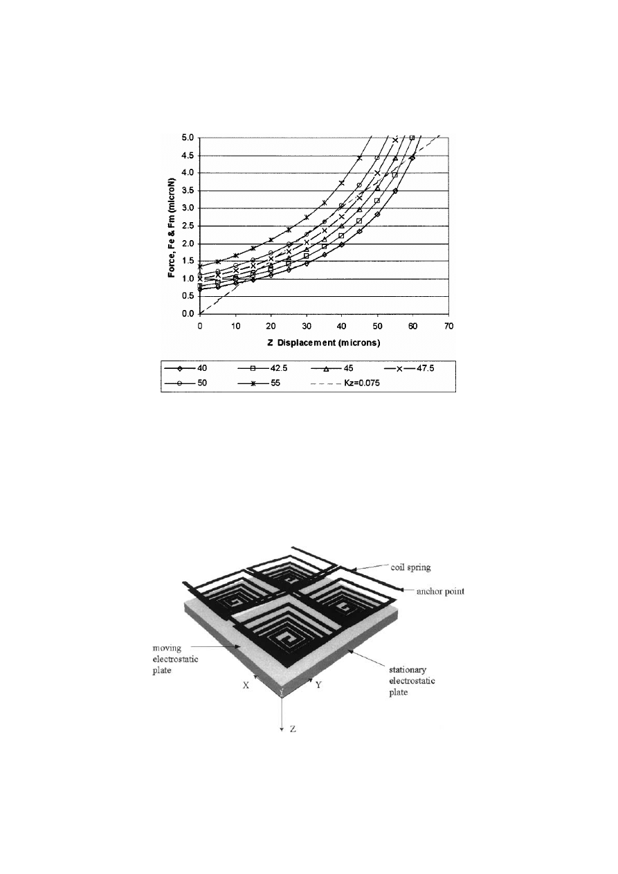
Figure 1 shows the theoretical plot of the above equa-
tion for actuation voltages of 40 volts to 55 volts. The
theoretical electrostatic force existing between the par-
allel plates at an instantaneous displacement from its
initial 100
µm gap position can be determined from the
respective constant voltage lines.
Superimposed in Fig. 1 is a line whose gradient rep-
resents the stiffness, K
z
, of a suspension system for
the moving electrostatic plate. Assuming a linear rela-
tionship, the mechanical restoring force, F
m
, from the
suspension system is related to it displacement
, Z, by
the equation;
F
m
= K
z
Z
(4)
and the instantaneous gap between the two electrostatic
plates is related to the displacement of the suspension
system by;
g
= (100 − Z)
(5)
40
Chong et al.
Fig. 1. Electrostatic and mechanical restoring forces at different displacement of the moving electrostatic plate.
This line shown in Fig. 1 has a gradient of K
z
=
0
.075 µN/µm and is tangent to the constant actuation
voltage line of 50 V. This represents the minimum pull
in voltage required for the electrostatic plates to snap
across the 100
µm gap. If an actuation voltage of 40 V is
applied, this suspension stiffness would result in a me-
chanical restoring force that equals to the electrostatic
force at a displacement of 12
µm or a gap of 88 µm.
Fig. 2. A quad-support, two-dimensional coil spring suspension system.
Using the same analogy, the suspension stiffness
required for different pull in voltages can be deter-
mined. To fulfill these stiffness requirements within a
confined footprint of 1 mm
× 1 mm, a quad-supported,
two-dimensional coil spring concept was implemented.
Figure 2 shows this suspension system in its actuated
mode. Each spring consists of 27 segments, each with
lengths varying from 45
µm to 490 µm and width of
Large Displacement Electrostatically Actuated Microrelay
41
Fig. 3. Process simulation window for device fabrication.
25
µm. The gap between the segments is 10 µm. The
different stiffnesses are achieved through different de-
position thicknesses, thus capitalizing on the advan-
tages associated to using a common mask.
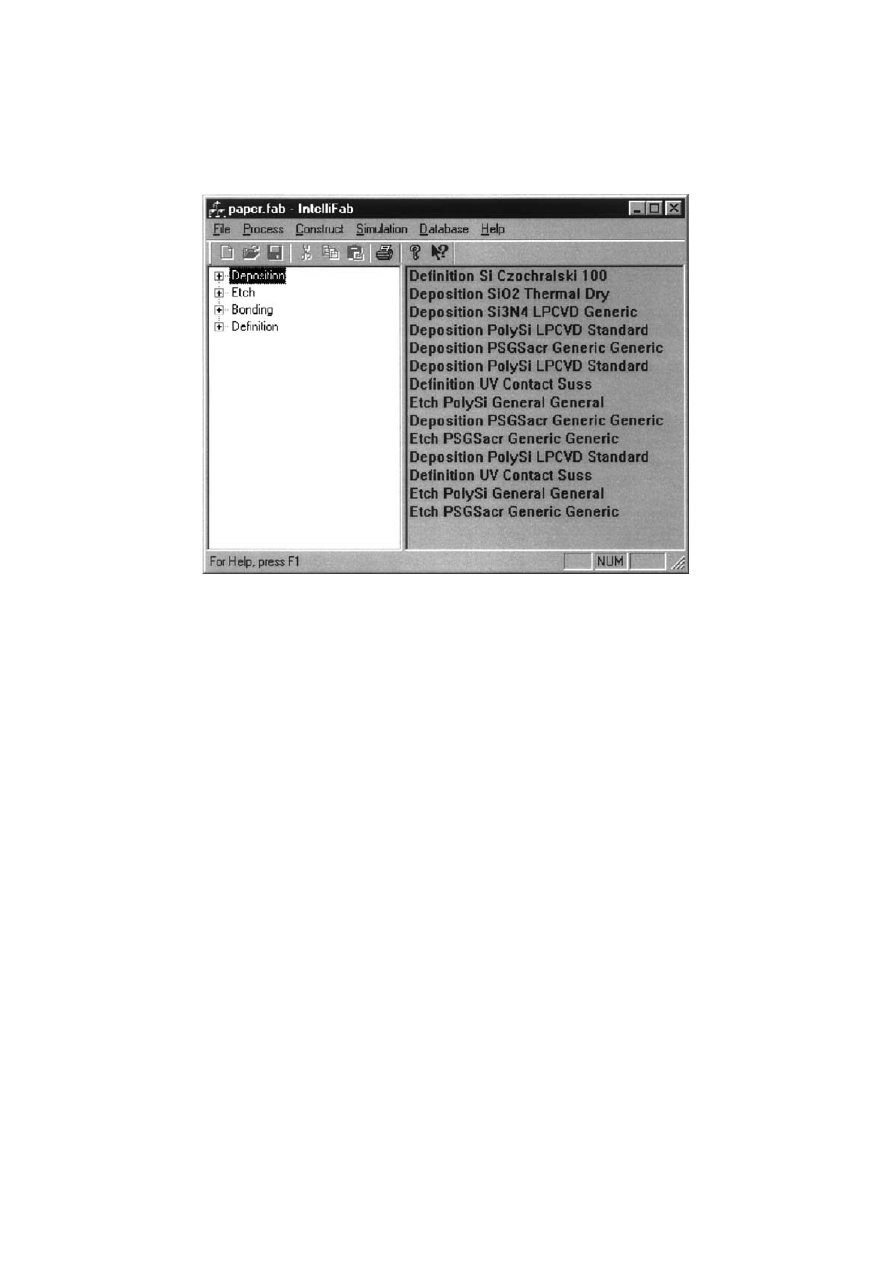
The fabrication feasibility of this design was eval-
uated in a detailed CAD simulation study using the
process simulation modules of IntelliSuite™ [36,39].
Figure 3 shows the key fabrication steps as shown in
IntelliFab™ process window. These key steps include
thermal oxide growth on silicon substrate (a quartz sub-
strate could be used if required, e.g., for various RF
applications) and addition of silicon nitride passiva-
tion layer. Then a doped polysilicon layer is deposited
using LPCVD process for the lower stationary elec-
trostatic plate (polysilicon). This is followed by a low
temperature sacrificial oxide deposition. Next a polysil-
icon layer is used for upper plate, and finally another
polysilicon layer is used for the quad springs. A dif-
ferent conductor layer can be used for top plate if an
etch stop is needed for creation of polysilicon springs.
The electrostatic plates are doped to attain a resistiv-
ity of 0.03 ohm-cm to accommodate the heat dissipa-
tion required during 3 Amps current surge for one sec-
ond. For contact materials, gold or gold contacts can be
used, however, it does restrict the subsequent fabrica-
tion steps (after gold electroplating) to low temperature
processes such as PECVD processes.
Subsequent to the fabrication simulation, a three-
dimensional solid model was created. Figure 4 shows
the device solid model before removal of sacrificial
layers. This model is then automatically meshed with
mechanical and electrical meshes. Coupled electrome-
chanical analysis was carried out using the Electrome-
chanical Analysis module of IntelliSuite™. A mesh
convergence study was also conducted to ensure result
accuracy.
4.
Results and Discussions
Results from detailed CAD simulation studies revealed
that device snapping is possible at different pull-in volt-
ages by varying the suspension stiffness. The quad-
suspension system is able to maintain plate paral-
lelism during the entire 100
µm travel. The electrostatic
pressure on the plate surfaces is uniformly distributed
throughout the entire surfaces and no tilting instability
was manifested.
Figure 5 shows the pull-in voltage of the microre-
lay with different suspension stiffnesses. The results
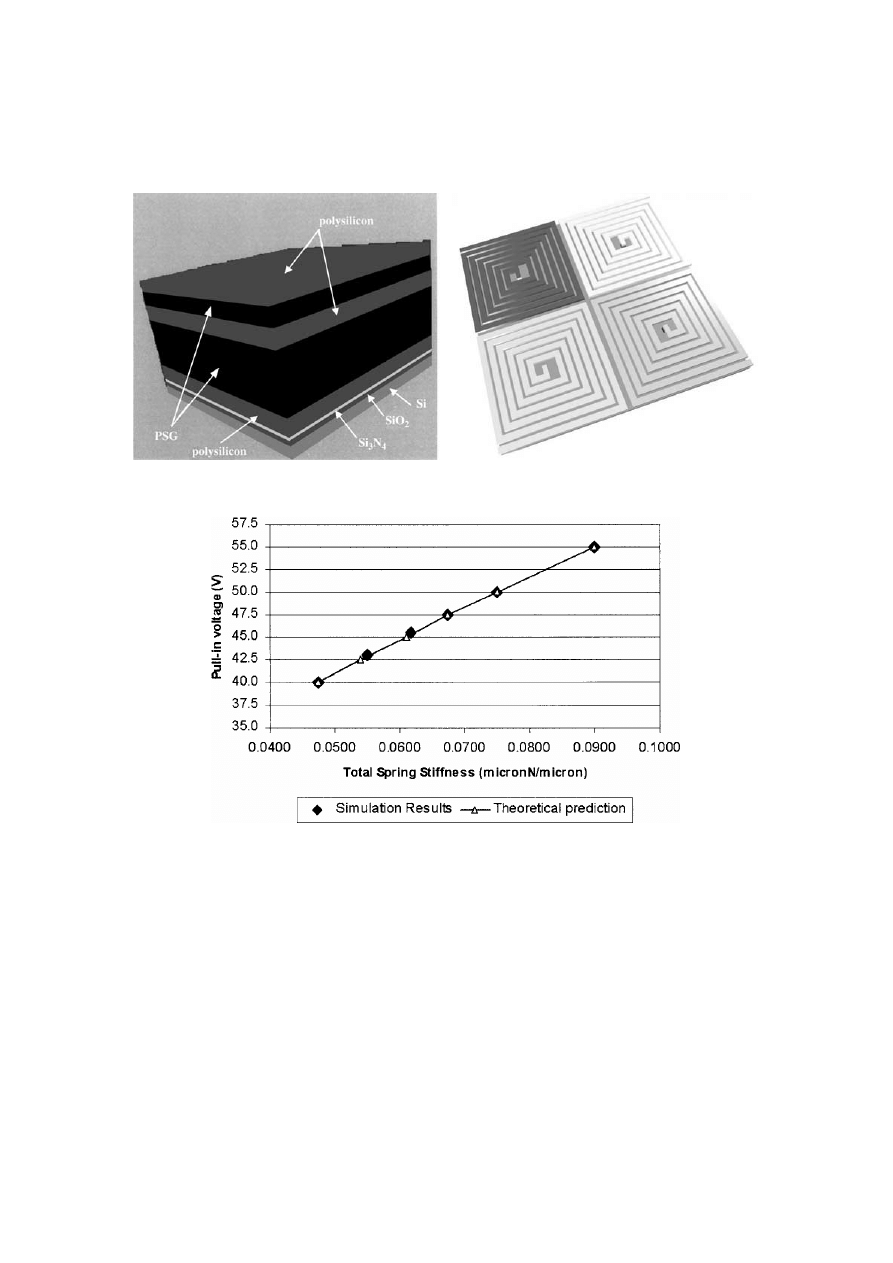
42
Chong et al.
Fig. 4. Solid model showing various fabrication layers (sacrificial layer not removed). Side and top views.
Fig. 5. Simulation results of pull-in voltages for different coil spring stiffnesses.
are in good agreement with theoretical predictions,
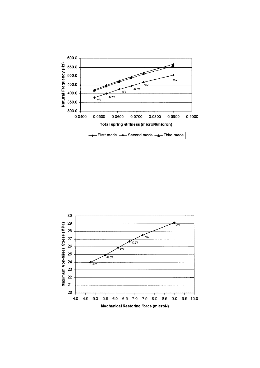
having a deviation of about 1%. The natural frequen-
cies of the device using different suspension stiffnesses
are depicted in Fig. 6. The first three modes of reso-
nance were analyzed. The first mode represents Z -axis
planar displacement of the moving electrostatic plate.
The second and third mode represents the out-of-plane
rotation of the plate about its axes of symmetry.
First mode resonance occurs at about 370 Hz to
500 Hz for suspension stiffnesses ranging from 0.0475
to 0.0900
µN/µm, corresponding to a pull-in voltage
range from 40 volts to 55 volts. Of particular interest,
the 50 volts pull-in voltage stiffness design resulted in a
first mode natural frequency of about 460 Hz. The out-
of-plane frequencies range is from 410 Hz to 570 Hz
for different spring stiffness. The slight difference of
about 2% between the second and third mode frequency
is due to the orientation of the coil spring anchor points.
From the functional aspect of the microrelay, these fre-
quencies are acceptable for its intended application.
However, considerable emphasis must be placed on the
package vibration isolation requirements if the relay is
required to operate in an external environment having
excitation frequency close to this range.
Large Displacement Electrostatically Actuated Microrelay
43
Fig. 6. Natural frequencies for different coil spring stiffnesses.
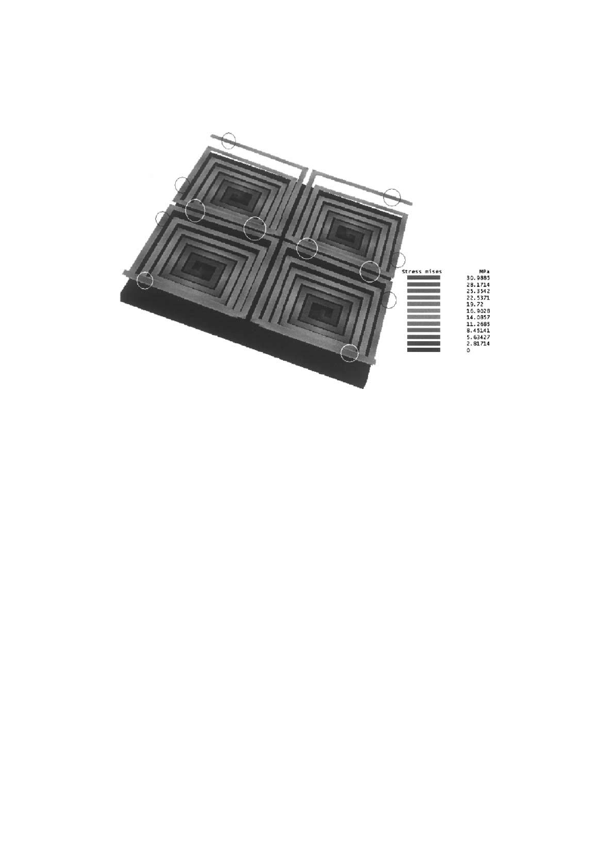
Stress analysis shows that the maximum Von-Mises
stress occurs near the turning point of each spring seg-
ment. These stresses with the corresponding restoring
force of the coil spring suspension system are depicted
in Fig. 7. For the 50 volts pull-in voltage design, the
Von-Mises stress is about 40% of the yield strength of
polysilicon (Fig. 8). These stress values could be fur-
ther reduced by reducing the stress concentration effect
due to the sharp corners of the spring design through
filleting.
Fig. 7. Maximum Von Mises stresses and restoring forces of the coil springs.
It should be noted that in this design, the mechan-
ical restoring force is the only mechanism to retrieve
the moving plate back to its initial position. This type
of relay (Type A-SPST) will work in condition when
low contact force is acceptable. If the environment has
moisture and propagates stiction, it will be difficult to
release the relay due to microweld formation in high
current switching applications. Various analytical mod-
els for stiction/adhesion (depending on type) are avail-
able in literature. However, no numerical solution or
44
Chong et al.
Fig. 8. Von Mises stresses for the device at 50 volts (maxima circled).
model exists that can explain or accurately predict stic-
tion during fabrication/release and stiction during op-
eration. A device operated in a vacuum will have a
lower moisture content and will be less susceptible to
stiction. However, in the interest of limiting the scope
of study, no research was performed on stiction issues.
Transient analyses (including determination of switch-
ing times and squeeze film damping effects) have not
yet been performed on the device. This design process
was dedicated to obtaining solutions to the steady-state
aspects of the design (e.g., spring constants, plate par-
allelism, pull-in voltage, etc.). The design parameters
are limited by the solutions to these problems, and by
varying these parameters (within the usable domain
determined during this process), the designer can opti-
mize the transient results. The settling time for the relay
after it breaks the contact has not been investigated. If
required, a physical breaking mechanism can be used
to avoid the oscillatory motion that may result after the
switch/contact breaks. Alternatively, a third electrode
placed above the spring suspension can be used to at-
tract the plate to its equilibrium position after the first
break occurs. The contact materials (usually gold or
gold-alloys), which significantly affect device opera-
tion and lifetime, require investigations. This study has
focused on a design and its variations and has shown
that through proper design, relatively large displace-
ments can be achieved using electrostatic actuation
mechanism. More research involving other practical
aspects, material issues, and fabrication requirements
can be done in the areas mentioned above.
5.
Conclusions
This simulation based design study has demonstrated
that with a carefully designed suspension system, it is
possible to achieve large displacement via electrostatic
actuation using a relatively small actuation voltage
over small surface dimensions. Its relevance has been
demonstrated on a microrelay with device specifica-
tions meeting stringent telecommunication equipment
requirements. The unique quad-supported, two-
dimensional coil spring suspension system is the key
principle of achieving the low stiffness required for the
device to function over tight footprint size. The device
mechanical characteristics are able to meet the device
functional expectations. Improvement of the mechani-
cal characteristics can be achieved through refining the
surface geometry of the coil spring. A circular spiral
coil spring design instead of a square coil spring would
certainly improve the mechanical characteristics.

Large Displacement Electrostatically Actuated Microrelay
45
References
1. Petersen, K. E., “Membrane switches on silicon.” IBM J. Res.
Develop. 23, pp. 376–385, 1979.
2. Trimmer, W. and Gabriel, K., “Design considerations for a
practical electrostatic micro-motor.” Sensors and Actuators 11,
pp. 189–206, 1987.
3. Brennen, R., Lim, M., Pisano, A. and Chou, A., “Large dis-
placement linear actuation.” Technical Digest IEEE Solid-State
Sensors and Actuators, pp. 135–139, June 1990.
4. Fukuda, T. and Tanaka, T., “Micro electro static actuator with
three degrees of freedom,” in Proc. IEEE Micro Electro Mechan-
ical Systems, NAPA Valley, pp. 153–158, 1990.
5. Gretillat, M., Thieubaud, P., de Rooij, N. and Linder, C., “Elec-
trostatic polysilicon microrelays integrated with MOSFETs,” in
Proc. IEEE Microelectromechanical Systems Conf., Oiso, Japan,
pp. 97–101, 1994.
6. Gretillat, M., Thieubaud, P., Linder, C. and de Rooij, N., “Inte-
grated circuit compatible electrostatic polysilicon microrelays.”
J. Micromech. Microeng. 5, pp. 156–160, 1995.
7. Roy, S. and Mehregany, M., “Fabrication of electrostatic nickel
microrelays by nickel surface micro-machining,” in Proc. IEEE
Microelectromechanical Sys. Conf., Amsterdam, Netherlands,
pp. 353–357, 1995.
8. Drake, J., Jerman, H., Lutze, B. and Stuber, M., in Proc. Trans.
’95, Stockholm, Sweden, 2, pp. 380–383, 1995.
9. Sakata, M., in Proc. IEEE MEMS Workshop, Salt Lake City,
pp. 149–151, 1989.
10. Yao, J. and Chang, M., in Proc. Trans. ’95, Stockholm,
Sweden, 2, pp. 384–387, 1995.
11. Gretillat,
M.,
Yang,
Y.,
Hung,
E.,
Rabinovich,
V.,
Ananthasuresh, G., DeRooij, N. and Senturia, S., “Nonlinear
electromechanical behavior of an electrostatic microrelay,” in
Proc. Int. Conf. Solid State Sensors and Actuators (Transducers
97), Chicago, 2, pp. 1141–1144, June 1997.
12. Maunder, S., McGuire, N., Arrack, P., Adams, G., Morrison, R.,
and Krum, J., “Measurements and modeling of surface micro
machined electrostatically actuated micro switches,” in Proc.
Int. Conf. Solid State Sensors and Actuators (Transducers 97),
Chicago, 2, pp. 1145–1148, June 1997.
13. Shield, I., Hill Erich, B., Kozlowski, F. and Evers, C., “Microme-
chanical relay with electrostatic actuation,” in Proc. Int. Conf.
Solid State Sensors and Actuators (Transducers 97), Chicago, 2,
pp. 1165–1168, June 1997.
14. Schlaak, H., Arndt, F. and Hanke, M., “Silicon microrelay—a
small signal relay with electrostatic actuator,” in Proc. 45th
Annual Int. Relay Conference, Lake Buena, FL, April 21–23,
1997, paper 10.
15. Zavracky, P., Majumder, S. and McGruer, N., “Microelectrome-
chanical switches fabricated using nickel surface micromachn-
ing.” J. Microelectromechanical Sys. 6(1), pp. 3–9, 1997.
16. Schlaak, H., Arndt, F., Schimkat, J. and Hanke, M., “Silicon
microrelay with electrostatic moving wedge actuator,” in Proc.
Fifth Int. Conf. on Microelectrooptomechanical Systems and
Components, Potsdam, pp. 463–468, 1996.
17. US Patents 5,051,643; 5,479,042; 5,627,396; 5,994,796;
5,578,976; 6,074,890; 6,057,520.
18. Chan, E. K. and Dutton, R. W., “Electrostatic micromechanical
actuator with extended range of travel.” J. Microelectromechan-
ical Systems 9(3), pp. 321–328, 2000.
19. Hosaka, H., Kuwano, H. and Yanagisawa, K., “Electro-
magnetic microrelays: Concepts and fundamental characteris-
tics,” in Proc. IEEE Microelectromechanical Sys. Conf., Fort
Lauderdale, pp. 12–17, 1993.
20. Hosaka, H., Kuwano, H. and Yanagisawa, K., “Electromagnetic
microrelays: Concepts and fundamental characteristics.” Sen-
sors and Actuators 40, pp. 41–47, 1994.
21. Hashimoto, E., Tanaka, H., Suzuki, Y., Uenishi, Y. and
Watabe, A., “Thermally controlled magnetization actuator
(TCMA) using thermosensitive magnetic materials,” in Proc.
IEEE Microelectromechanical Systems Conference, Oiso, Japan,
pp. 108–113, 1994.
22. Hosaka, H. and Kuwano, H., “Ultra-small matrix relay for
telecommunications systems.” Oric. IEEE Forum on Micro-
machine and Micromechatronics, Nagoya, Japan, pp. 154–159,
1995.
23. Rogge, B., Schulz, J., Mohr, J., Thommes, A. and Menz, W.,
“Fully batch fabricated magnetic microactuators using a two
layer LIGA process,” in Proc. Transducers 95, Stockholm 1,
pp. 320–323, 1995.
24. Ziad, H., Debruker, D., Chevrier, J.-B., Baert, K., Lowe, H. and
Tilmans, H., “Towards Integrated microrelays using electromag-
netic actuation,” in Proc. Eurosensors X, Belgium, pp. 1193–
1196, 1996.
25. Wright, J., Tai, Y. and Chang, S., “A large force fully integrated
MEMS magnetic actuator,” in Proc. Transducers 97, Chicago, 2,
pp. 793–796, 1997.
26. Taylor, W., “The design and fabrication of fully integrated mag-
netically actuated micromachined relays.” Doctoral dissertation,
Georgia Institute of Technology, November 1997.
27. US patents 6,094,116; 5,847,631; 5,757,255; 5,969,586;
6,043,730;
6,078,233;
5,880,654;
5,790,004;
5,880,653;
5,748,061; 5,986,529; 5,872,496; 5,778,513; 5,398,011.
28. Seki, T., Sakata, M., Nakajima, T. and Matsumoto, M., “Thermal
buckling actuator for micro relays,” in Proc. Transducers 97,
Chicago, 2, pp. 11153–11156, 1997.
29. Simon, J., Saffer, S. and Kim, C., “A micromechanical relay with
thermally driven mercury micro drop,” in Proc. IEEE Microelec-
tromechanical Sys. Conf., San Diego, pp. 515–520, 1996.
30. Goldman, K. and Mehregany, M., “A novel micromechan-
ical temperature memory sensor,” in Proc. Transducers 95,
Stockholm, 2, pp. 132–135, 1995.
31. Tomonari, S., Piccinic, J., Yoshida, H., Ogihara, J., Nagao,
S., Saito, M., Kawahito, K. and Kawada, H., “The microrelay
thermally actuated by the silicon bimetal.” NARM Conference,
2000.
32. http://www.sma-mems.com/microrly.htm.
33. Carlen, E. and Mastrangelo, C., “Simple high actuation power,
thermally activated paraffin microactuator.” Transducers 99,
Sendai, Japan, 2, pp. 1364–1367, June 7–10 1999.
34. US patent 5,467,068.
35. US patent 5,994,816; 5,955,817; 6,023,121.
36. IntelliSuite™ version 5.1–Users Manual.
37. Engineers relay handbook, National association of relay manu-
facturers, Milwaukee, WI, 5th edition, pp. 3–20, 1966.
38. Cheng, D., Field and Wave Electromagnetics, Reading
Edison-Wesley Publishing Company, 1990.
46
Chong et al.
39. He, Y., Marchetti, J. and Maseeh, F., “MEMS computer-aided
design,” in Proc. European Design & Test Conference and
Exhibition on Microfabrication, Paris, France, 1997.
Gooi Boon Chong received the B. Eng (Hons)
degree in mechanical engineering from the National
University of Singapore in 1989 and the M. Eng degree
in fluid mechanics from the Nanyang Technological
University, Singapore in 1992. He is presently an aca-
demic staff with the School of Engineering, Nanyang
Polytechnic, Singapore. His current research interest
is in the design of MEMS devices for bio-medical
applications.
Kam See Hoon received the B. Eng (Hons) degree
in electrical engineering from the National University
of Singapore in 1990. He is presently an academic staff
with the School of Engineering, Nanyang Polytechnic,
Singapore. His current research interest is in the design
of MEMS devices used in photonics applications.
Ijaz H. Jafri received his Bachelor of Science in
mechanical engineering from New York Institute of
Technology (1993). He received his Masters of Science
(1994) and Ph.D. (1999) also in mechanical engineer-
ing from the State University of New York at Stony
Brook. Since 1996, while working at GT Equipment
Technologies, Inc., he conducted research for develop-
ing new systems and technologies for III–V compound
semiconductors, bulk polysilicon growth, purification
of metallurgical grade silicon for photovoltaic indus-
try, critical point drying for MEMS, and supercriti-
cal fluid based photoresist removal for semiconductor
industry. After joining Corning Intellisense in 2000,
he has been conducting applied research, design and
development in MEMS technology. He holds various
patents in MEMS and semiconductor technologies. His
publications and research interests in MEMS design
and process include thermally and electrostatically ac-
tuated devices, micro hot plate sensors, microrelays,
microswitches, micromirrors, stiction in MEMS, and
microfluidics applications.
Daniel J. Keating received a Master of Science
degree in mechanical engineering from M.I.T. While
taking classes in Product Design and Development,
Inventions and Patents, Finite Element Analysis, and
Engineering Mathematics, he performed research in
the field of numerical model accuracy and verification
for the Engineering Analysis group (ESA-EA) at the
Los Alamos National Laboratory in New Mexico. He
also did his undergraduate studies at M.I.T., receiving a
Bachelor of Science degree in mechanical engineering.
He is presently Senior applications engineer at Corning
Intellisense.
Wyszukiwarka
Podobne podstrony:
10 Large Displacement Electrostatically Actuated Microrelay
16 Electrostatic actuators with P silicon diaphragms
16 Electrostatic actuators with P silicon diaphragms
PP MEMS 03 Electrostatic Actuation
13 IMPROVING ELECTROSTATIC ACTUATORS for micro mirrors
14 MOEMS Switch Device with Electrostatic Actuator
Samsung GT P5210 Galaxy Tab 3 10 1 05 Main electrical parts list
Elektor Electronics No 10 10 2011
electraplan cennik 10 10 09
Electrostatic micro actuator for HD
electraplan cennik 10 10 09
Everyday Practical Electronics 2001 10
Electrolysis (10)
Elektor Electronics No 10 10 2011
01 Capacitance based model for electrostatic micro actuators
10 Vintage Christmas Display Patterns Woodworking Yard Art
Everyday Practical Electronics 2001 10
więcej podobnych podstron