TDA7297
15+15W DUAL BRIDGE AMPLIFIER
WIDE SUPPLY VOLTAGE RANGE (6V -18V)
MINIMUM EXTERNAL COMPONENTS
– NO SVR CAPACITOR
– NO BOOTSTRAP
– NO BOUCHEROT CELLS
– INTERNALLY FIXED GAIN
STAND-BY & MUTE FUNCTIONS
SHORT CIRCUIT PROTECTION
THERMAL OVERLOAD PROTECTION
DESCRIPTION
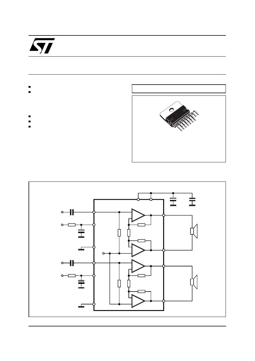
The TDA7297 is a dual bridge amplifier specially
designed for TV and Portable Radio applications.
September 2003
®
1
2
4
Vref
ST-BY
7
IN1
0.22
µ
F
VCC
13
3
D94AU175B
+
-
-
+
OUT1+
OUT1-
15
14
12
MUTE
6
IN2
0.22
µ
F
+
-
-
+
OUT2+
OUT2-
8
9
S-GND
PW-GND
470
µ
F
100nF
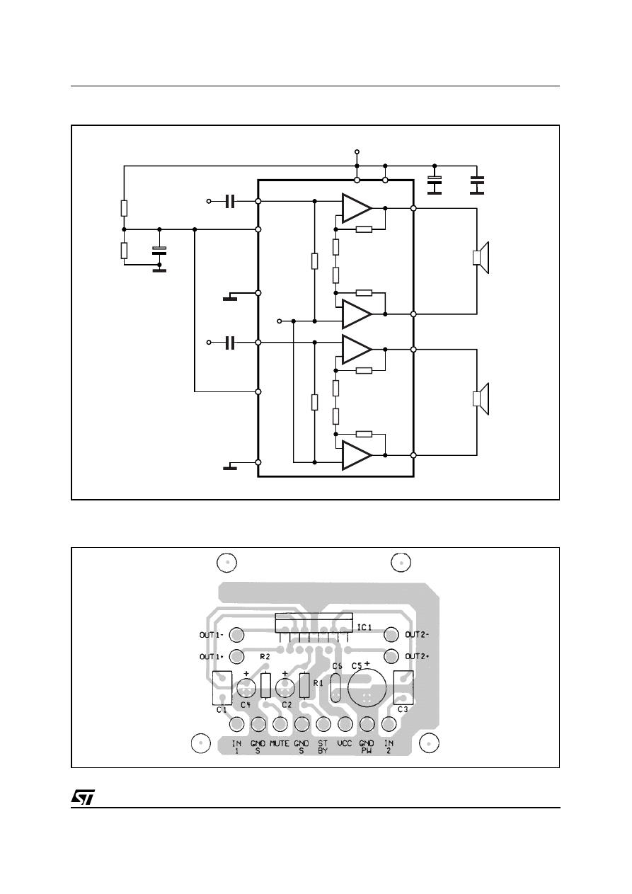
BLOCK AND APPLICATION DIAGRAM
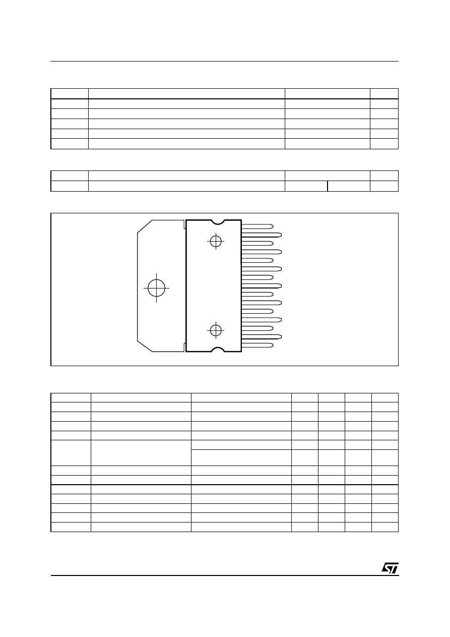
Multiwatt 15
ORDERING NUMBER: TDA7297
TECHNOLOGY BI20II
1/9
1
2
3
4
5
6
7
9
10
11
8
N.C.
N.C.
S-GND
PW-GND
ST-BY
MUTE
N.C.
IN1
V
CC
OUT1-
OUT1+
13
14
15
12
OUT2+
OUT2-
VCC
IN2
D95AU261
PIN CONNECTION (Top view)
ABSOLUTE MAXIMUM RATINGS
Symbol
Parameter
Value
Unit
V
S
Supply Voltage
20
V
I
O
Output Peak Current (internally limited)
2
A
P
tot
Total Power Dissipation (T
case
= 70
°
C)
33
W
T
op
Operating Temperature
0 to 70
°
C
T
stg
, T
j
Storage and Junction Temperature
-40 to +150
°
C
THERMAL DATA
Symbol
Description
Value
Unit
R
th j-case
Thermal Resistance Junction to case
Typ. 1.4
Max. 2
°
C/W
ELECTRICAL CHARACTERISTICS (V
CC
= 16.5V, R
L
= 8
Ω
, f = 1kHz, T
amb
= 25
°
C unless otherwise
specified.)
Symbol
Parameter
Test Condition
Min.
Typ.
Max.
Unit
V
CC
Supply Range
6.5
18
V
I
q
Total Quiescent Current
R
L
=
∞
50
65
mA
V
OS
Output Offset Voltage
120
mV
P
O
Output Power
THD = 10%
13
15
W
THD
Total Harmonic Distortion
P
O
= 1W
0.1
0.3
%
P
O
= 0.1W to 5W
f = 100Hz to 15kHz
1
%
SVR
Supply Voltage Rejection
f = 100Hz V
R
= 0.5V
40
56
dB
CT
Crosstalk
46
60
dB
A
MUTE
Mute Attenuation
60
80
dB
T
W
Thermal Threshold
150
°
C
G
V
Closed Loop Voltage Gain
31
32
33
dB
∆
Gv
Voltage Gain Matching
0.5
dB
R
i
Input Resistance
25
30
K
Ω
TDA7297
2/9
1
2
4
Vref
ST-BY
7
IN1
C1 0.22
µ
F
VCC
13
3
D95AU258A
+
-
-
+
OUT1+
OUT1-
15
14
12
MUTE
6
IN2
C3 0.22
µ
F
+
-
-
+
OUT2+
OUT2-
8
9
S-GND
PW-GND
C5
470
µ
F
C6
100nF
R1 10K
C2
10
µ
F
µ
P
R2 10K
C4
1
µ
F
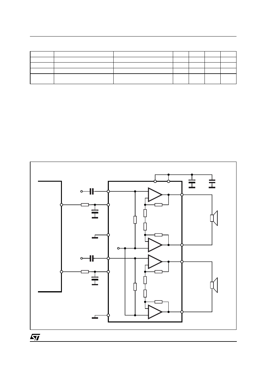
Figure 1: Microprocessor Application
ELECTRICAL CHARACTERISTICS (Continued)
Symbol
Parameter
Test Condition
Min.
Typ.
Max.
Unit
VT
MUTE
Mute Threshold
V
O
= -30dB
2.3
2.9
4.1
V
VT
ST-BY
St-by Threshold
0.8
1.3
1.8
V
I
ST-BY
ST-BY current V6 = GND
100
µ
A
e
N
Total Output Noise Voltage
A curve
f = 20Hz to 20kHz
150
220
500
µ
V
µ
V
APPLICATION SUGGESTION
STAND-BY AND MUTE FUNCTIONS
(A) Microprocessor Application
In order to avoid annoying "Pop-Noise" during
Turn-On/Off transients, it is necessary to guaran-
tee the right St-by and mute signals sequence.
It is quite simple to obtain this function using a mi-
croprocessor (Fig. 1 and 2).
At first St-by signal (from mP) goes high and the
voltage across the St-by terminal (Pin 7) starts to
increase exponentially. The external RC network
is intended to turn-on slowly the biasing circuits of
the amplifier, this to avoid "POP" and "CLICK" on
the outputs.
When this voltage reaches the St-by threshold
level, the amplifier is switched-on and the external
capacitors in series to the input terminals (C3,
C5) start to charge.
It’s necessary to mantain the mute signal low until
the capacitors are fully charged, this to avoid that
the device goes in play mode causing a loud "Pop
Noise" on the speakers.
A delay of 100-200ms between St-by and mute
signals is suitable for a proper operation.
TDA7297
3/9
+V
S
(V)
V
IN
(mV)
V
ST-BY
pin 7
I
q
(mA)
ST-BY
MUTE
PLAY
MUTE
ST-BY
+18
1.8
0.8
V
MUTE
pin 6
4.1
2.3
OFF
OFF
D96AU259
V
OUT
(V)
2.9
1.3
Figure 2: Microprocessor Driving Signals.
(B) Low Cost Application
In low cost applications where the mP is not pre-
sent, the suggested circuit is shown in fig.3.
The St-by and mute terminals are tied together
and they are connected to the supply line via an
external voltage divider.
The device is switched-on/off from the supply line
and the external capacitor C4 is intended to delay
the St-by and mute threshold exceeding, avoiding
"Popping" problems.
TDA7297
4/9
1
2
4
Vref
ST-BY
7
IN1
C3 0.22
µ
F
VCC
13
3
D95AU260A
+
-
-
+
OUT1+
OUT1-
15
14
12
MUTE
6
IN2
C5 0.22
µ
F
+
-
-
+
OUT2+
OUT2-
8
9
S-GND
PW-GND
C1
470
µ
F
C2
100nF
R1
47K
C4
10
µ
F
R2
47K
Figure 3: Stand-alone Low-cost Application.
Figure 3b: PCB and Component Layout of the Application Circuit (Fig. 1).
TDA7297
5/9
0.01 0
0 .1
1
1 0
0 .1
1
1 0
2 0
TH D(%)
Vc c = 1 6.5V
R l = 8 ohm
f = 15 KH z
f = 5K H z
f = 1K H z
P out (W )
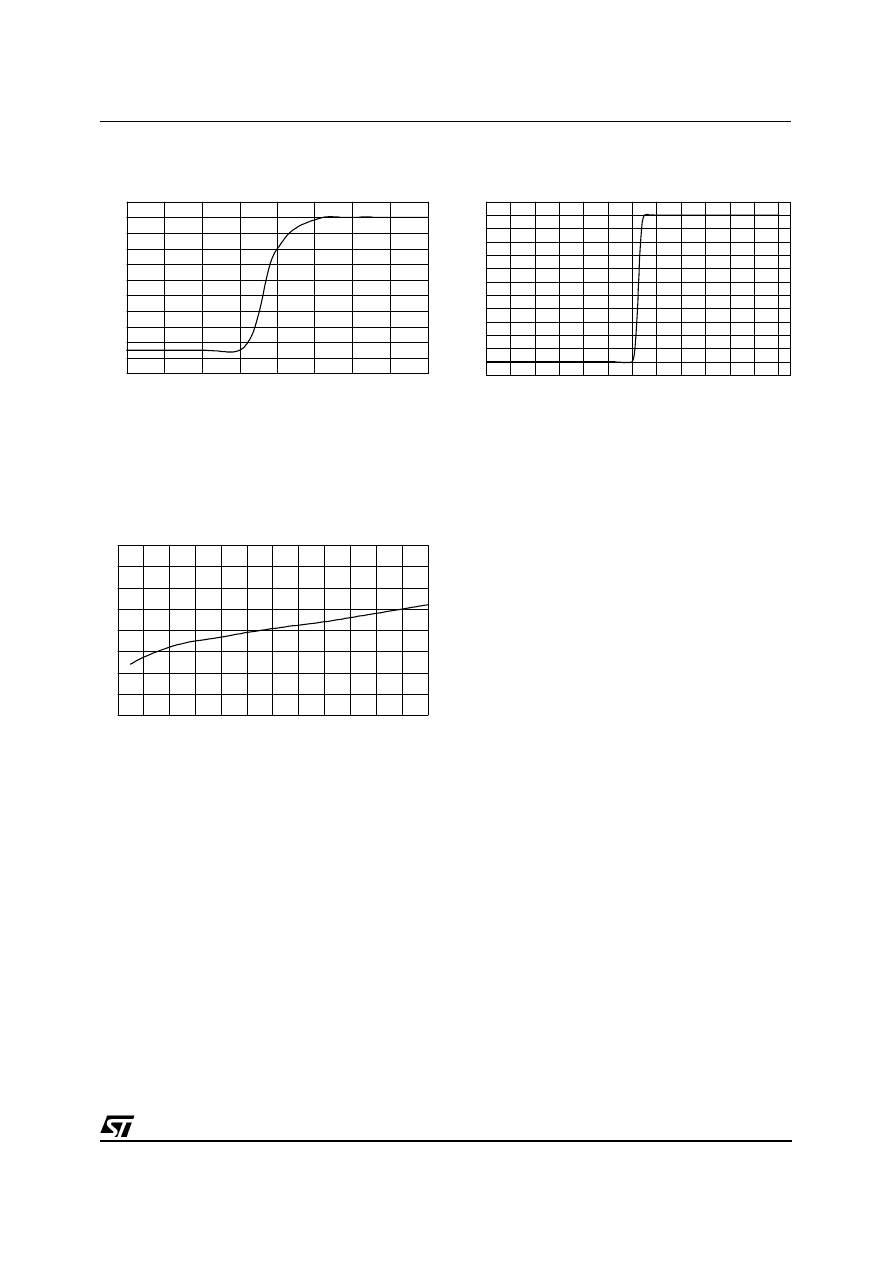
Figure 4: Distortion vs Output Power
0.0 1 0
0.1
1
10
0.1
1
10
TH D (% )
Vc c = 12 V
R l = 8 o hm
f = 1 5 K H z
f = 5 K H z
f = 1 K H z
P ou t (W )
Figure 5: Distortion vs Output Power
0 .0 10
0 .1
1
1 0
1 0 0
1 k
1 0 k
2 0 k
T H D (% )
V c c = 1 6.5 V
R l = 8 o hm
P o ut = 1 0 0 m W
P o ut = 5 W
fre q ue n c y (H z)
Figure 6: Distortion vs Frequency
-5.00 0
-4.00 0
-3.00 0
-2.00 0
-1.00 0
0.0
1.00 0 0
2.00 0 0
3.00 0 0
4.00 0 0
5.00 0 0
10
10 0
1k
10 k
10 0 k
Le ve l(d B r)
fre q ue nc y (Hz )
V c c = 1 6 .5 V
R l = 8 o h m
P o u t = 1 W
Figure 7: Frequency Respone
0.0
2.00 00
4.00 00
6.00 00
8.00 00
10 .0 00
12 .0 00
14 .0 00
16 .0 00
18 .0 00
20 .0 00
6.0 00 7.0 00 8.0 00 9.0 00 10.00 11 .00 12.00 13.00 14.00 15 .00 16.00 17 .00 18.00
P o(W
)
V s(V )
R l = 8 o h m
f = 1K H z
d = 10 %
d = 1%
Figure 8: Output Power vs Supply Voltage
0
1
2
3
4
5
6
7
8
9
10 11 12 13 14 15 16
0
2
4
6
8
10
12
14
16
0
5
10
15
20
25
30
35
40
45
50
55
60
65
70
75
80
Ptot(W)
µ(%)
2XPout(W)
Vcc = 16.5V
Rl = 8ohm (both channels)
f = 1KHz
P tot
µ
Figure 9: Total Power Dissipation & Efficiency vs
Output Power
TDA7297
6/9
6
7
8
9
10
11
12
13
14
15
16
17
18
30
35
40
45
50
55
60
65
70
Iq (mA)
Vsupply(V)
Figure 12: Quiscent Current vs. Supply Voltage
1
1.5
2
2.5
3
3.5
4
4.5
5
0
10
-10
-20
-30
-40
-50
-60
-70
-80
-90
-100
Attenuation (dB)
Vpin.6(V)
Figure 10: Mute Attenuation vs. V pin.6
0
0.2
0.4
0.6
0.8
1
1.2
1.4
1.6
1.8
2
2.2
2.4
0
10
-10
-20
-30
-40
-50
-60
-70
-80
-90
-100
-110
-120
Attenuation (dB)
Vpin.7 (V)
Figure 11: Stand-By Attenuation vs Vpin.7
TDA7297
7/9
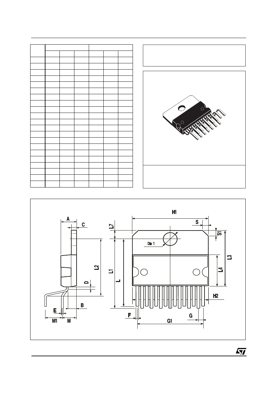
Multiwatt15 V
DIM.
mm
inch
MIN.
TYP.
MAX.
MIN.
TYP.
MAX.
A
5
0.197
B
2.65
0.104
C
1.6
0.063
D
1
0.039
E
0.49
0.55
0.019
0.022
F
0.66
0.75
0.026
0.030
G
1.02
1.27
1.52
0.040
0.050
0.060
G1
17.53
17.78
18.03
0.690
0.700
0.710
H1
19.6
0.772
H2
20.2
0.795
L
21.9
22.2
22.5
0.862
0.874
0.886
L1
21.7
22.1
22.5
0.854
0.870
0.886
L2
17.65
18.1
0.695
0.713
L3
17.25
17.5
17.75
0.679
0.689
0.699
L4
10.3
10.7
10.9
0.406
0.421
0.429
L7
2.65
2.9
0.104
0.114
M
4.25
4.55
4.85
0.167
0.179
0.191
M1
4.63
5.08
5.53
0.182
0.200
0.218
S
1.9
2.6
0.075
0.102
S1
1.9
2.6
0.075
0.102
Dia1
3.65
3.85
0.144
0.152
OUTLINE AND
MECHANICAL DATA
TDA7297
8/9

Information furnished is believed to be accurate and reliable. However, STMicroelectronics assumes no responsibility for the consequences
of use of such information nor for any infringement of patents or other rights of third parties which may result from its use. No license is
granted by implication or otherwise under any patent or patent rights of STMicroelectronics. Specifications mentioned in this publication are
subject to change without notice. This publication supersedes and replaces all information previously supplied. STMicroelectronics products
are not authorized for use as critical components in life support devices or systems without express written approval of STMicroelectronics.
The ST logo is a registered trademark of STMicroelectronics.
All other names are the property of their respective owners
© 2003 STMicroelectronics - All rights reserved
STMicroelectronics GROUP OF COMPANIES
Australia – Belgium - Brazil - Canada - China – Czech Republic - Finland - France - Germany - Hong Kong - India - Israel - Italy - Japan -
Malaysia - Malta - Morocco - Singapore - Spain - Sweden - Switzerland - United Kingdom - United States
www.st.com
TDA7297
9/9
Wyszukiwarka
Podobne podstrony:
Schemat wzmacniacza Mullard
Schemat wzmacniacza PW 3015
Schemat wzmacniacz
NE013 WZMACNIACZ MONO TDA7294 1x100W
NE013 WZMACNIACZ MONO TDA7294, 1x100W
Schemat połączeniowy wideodomofonu (Urmet-MR-2) bez-wzmacniacza
Przedwzmacnipreamp lampowy do LM3875, opis i schemat, Na stronie Wzmacniacz na LM 3875 opisałem budo
2003 07 Uniwersalny Moduł TDA7294, czyli prosta droga do wzmacniacza multimedialnego 6x100W
Schemat stanowiska pomiarowego do?dania wzmacniacza operacyjnego przedstawiono na rysunku poniżej
Jak zbudować wzmacniacz na TDA7294, ELEKTRONIKA, Wzmacniacze
NE013 WZMACNIACZ MONO TDA7294 1x100W
STA 700 wzmacniacz estradowy schemat końcówki mocy
Wzmacniacz 300W Schemat 300W
Wzmacniacz schemat
więcej podobnych podstron