.
LARGE VOLTAGE GAIN : 100dB
.
VERY LOW SUPPLY CURRENT/AMPLI :
375
µ
A
.
LOW INPUT BIAS CURRENT : 20nA
.
LOW INPUT OFFSET CURRENT : 2nA
.
WIDE POWER SUPPLY RANGE :
SINGLE SUPPLY : +3V TO +30V
DUAL SUPPLIES :
±
1.5V TO
±
15V
DESCRIPTION
This circuit consists of four independent, high gain,
internally frequency compensated operational am-
plifiers which were designed specifically for automo-
tive and industrial control systems. It operates from
a single power supply over a wide range of
volt-
ages. Operation from split power supplies is also
possible and the low power supply current drain is
independent of the magnitude of the power supply
voltage.
In ve rtin g In p u t 2
Non-inv ert ing In pu t 2
N o n -i nv e r ti n g In p u t 1
CC
V
-
CC
V
1
2
3
4
8
5
6
7
9
1 0
1 1
1 2
1 3
1 4
+
O utput 3
Ou tp u t 4
N o n - in ve r tin g In p u t 4
Inverti ng Input 4
Non-inve rt ing In pu t 3
In ve rtin g In p u t 3
-
+
-
+
-
+
-
+
Ou tp u t 1
Inv erti ng Input 1
O utput 2
2902-01.EPS
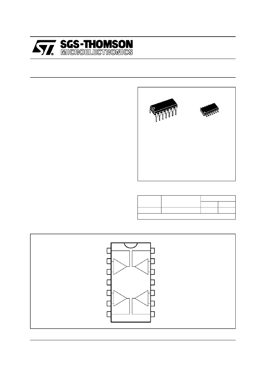
PIN CONNECTIONS (top view)
ORDER CODES
Part
Number
Temperature
Range
Package
N
D
LM2902
-40
o
C, +125
o
C
•
•
Example : LM2902D
2902-01.TBL
N
DIP14
(Plastic Package)
D
SO14
(Plastic Micropackage)
LOW POWER QUAD OPERATIONAL AMPLIFIERS
LM2902
November 1995
1/11
ABSOLUTE MAXIMUM RATINGS
Symbol
Parameter
Value
Unit
V
cc
Supply Voltage
±
16 or 32
V
V
i
Input Voltage
-0.3 to +32
V
V
id
Differential Input Voltage
+32
V
P
tot
Power Dissipation
N Suffix
D Suffix
500
400
mW
mW
-
Output Short-circuit Duration - (note 1)
Infinite
I
in
Input Current – (note 6)
50
mA
T
oper
Operating Free Air Temperature Range
-40 to +125
o
C
T
stg
Storage Temperature Range
-65 to +150
o
C
2902-02.TBL
6
µ
A
4
µ
A
100
µ
A
Q2
Q3
Q4
Q1
Inverting
input
Non-inverting
input
Q8
Q9
Q10
Q11
Q12
50
µ
A
Q13
Output
Q7
Q6
Q5
R
SC
V
CC
C
C
GND
2902-02.EPS
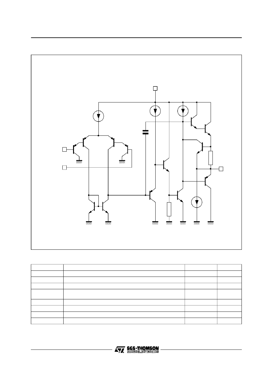
SCHEMATIC DIAGRAM (1/4 LM2902)
LM2902
2/11
ELECTRICAL CHARACTERISTICS
V
CC
+
= +5V, V
CC
–
= Ground, V
O
= 1.4V, T
amb
= +25
o
C
(unless otherwise specified)
Symbol
Parameter
Min.
Typ.
Max.
Unit
V
io
Input Offset Voltage (note 3)
T
amb
= +25
o
C
T
min.
≤
T
amb
≤
T
max
.
2
7
9
mV
I
io
Input Offset Current
T
amb
= +25
o
C
T
min.
≤
T
amb
≤
T
max
.
2
30
40
nA
I
ib
Input Bias Current (note 2)
T
amb
= +25
o
C
T
min.
≤
T
amb
≤
T
max
.
20
150
200
nA
A
vd
Large Signal Voltage Gain
(V
CC
+
= +15V, R
L
= 2k
Ω
, V
O
= 1.4V to 11.4V)
T
amb
= +25
o
C
T
min.
≤
T
amb
≤
T
max
.
50
25
100
V/mV
SVR
Supply Voltage Rejection Ratio (R
S
≤
10k
Ω
)
(V
CC
+
= 5V to 30V)
T
amb
= +25
o
C
T
min.
≤
T
amb
≤
T
max
.
65
65
110
dB
I
CC
Supply Current, all Amp, no load
T
amb
= +25
o
C
V
CC
= +5V
V
CC
= +30V
T
min.
≤
T
amb
≤
T
max
.
V
CC
= +5V
V
CC
= +30V
0.7
1.5
0.8
1.5
1.2
3
1.2
3
mA
V
icm
Input Common Mode Voltage Range
(V
CC
= +30V) - (note 4)
T
amb
= +25
o
C
T
min.
≤
T
amb
≤
T
max.
0
0
V
CC
-1.5
V
CC
-2
V
CMR
Common-mode Rejection Ratio (R
S
≤
10k
Ω
)
T
amb
= +25
o
C
T
min.
≤
T
amb
≤
T
max
70
60
80
dB
I
o
Output Short-circuit Current (V
id
= +1V)
V
CC
= +15V, V
o
= +2V
20
40
60
mA
I
sink
Output Sink Current (V
id
= -1V)
V
CC
= +15V, V
o
= +2V
V
CC
= +15V, V
o
= +0.2V
10
12
20
50
mA
µ
A
2902-03.TBL
LM2902
3/11
ELECTRICAL CHARACTERISTICS (continued)
Symbol
Parameter
Min.
Typ.
Max.
Unit
V
OH
High Level Output Voltage
(V
CC
= +30V)
T
amb
= +25
o
C
R
L
= 2k
Ω
T
min
.
≤
T
amb
≤
T
max
.
T
amb
= +25
o
C
R
L
= 10k
Ω
T
min
.
≤
T
amb
≤
T
max
.
(V
CC
= +5V, R
L
= 2k
Ω)
T
amb
= +25
o
C
T
min
.
≤
T
amb
≤
T
max
.
26
26
27
27
3.5
3
27
28
V
V
OL
Low Level Output Voltage (R
L
= 10k
Ω
)
T
amb
= +25
o
C
T
min
.
≤
T
amb
≤
T
max
.
5
20
20
mV
SR
Slew Rate (V
CC
= 15V, V
I
= 0.5 to 3V,
R
L
= 2k
Ω
, C
L
= 100pF, T
amb
= +25
o
C,
unity gain)
0.4
V/
µ
s
GBP
Gain Bandwidth Product (V
CC
= 30V
f = 100kHz, T
amb
= +25
o
C, V
in
= 10mV
R
L
= 2k
Ω
, C
L
= 100pF)
1.3
MHz
THD
Total Harmonic Distortion
(f = 1kHz, A
V
= 20dB, R
L
= 2k
Ω
, V
O
= 2V
pp
C
L
= 100pF, T
amb
= +25
o
C, V
CC
= 30V)
0.015
%
e
n
Equivalent Input Noise Voltage
(f = 1kHz, R
s
= 100
Ω
, V
CC
= 30V)
40
nV
√
Hz
DV
io
Input Offset Voltage Drift
7
30
µ
V/
o
C
DI
IO
Input Offset Current Drift
10
200
pA/
o
C
V
O
1/V
O
2
Channel Separation (note 5)
1kHz
≤
f
≤
20kHz
120
dB
2902-04.TBL
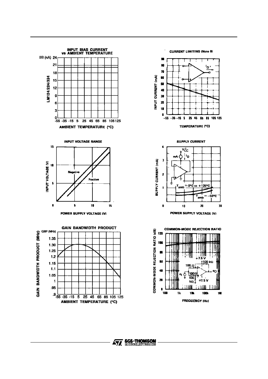
Not es :
1. Shor t - ci rcui t s f rom t he out put t o V
C C
can cause excessive heati ng if V
C C
> 15V. The maximum out put cur rent
i s approximatel y 40mA i ndependent of t he magni tude of V
C C
. Destr uct ive di ssipat i on can resul t f r om si mul t a-
neous short - ci rcuit on all ampl i fi ers.
2. The di r ect ion of t he i nput curr ent i s out of the IC. T his cur r ent i s essent iall y constant, independent of the stat e
of t he out put so no l oadi ng change exi st s on t he input l i nes.
3. V
o
= 1. 4V , R
s
= 0
Ω,
5V < V
C C
+
< 30V , 0 < V
ic
< V
C C
+
- 1.5V
4. The i nput common-mode volt age of ei ther i nput si gnal volt age should not be all owed to go negati ve by more
t han 0.3V. T he upper end of t he comm on-mode vol tage r ange i s V
C C
+
- 1. 5V, but ei ther or bot h i nputs can go
t o + 32V w i thout damage.
5. D ue t o t he pr oxi mi ty of exter nal component s insure t hat coupling i s not ori gi nat ing vi a st ray capacit ance be-
t w een these ext ernal par ts. T hi s t ypi call y can be detect ed as this type of capaci t ance i ncreases at hi gher f re-
quences.
6. Thi s input curr ent onl y exi sts when the volt age at any of the i nput leads i s dri ven negat iv e. I t is due t o t he
coll ect or -base junct i on of the input PN P t ransi st or becom ing forw ar d bi ased and thereby acti ng as input di-
odes clamps. I n addi t i on to thi s di ode acti on, there i s al so N PN parasi ti c act ion on t he I C chi p. t hi s t ransi st or
acti on can cause t he output vol t ages of the Op- amps to go t o the V
CC
vol tage l evel (or t o ground for a l arge
over dr i ve) f or t he t i me durati on t han an i nput i s dri ven negat ive.
T hi s i s not dest r ucti ve and nor mal out put w i ll set up agai n f or input vol t age higher than - 0. 3V.
LM2902
4/11
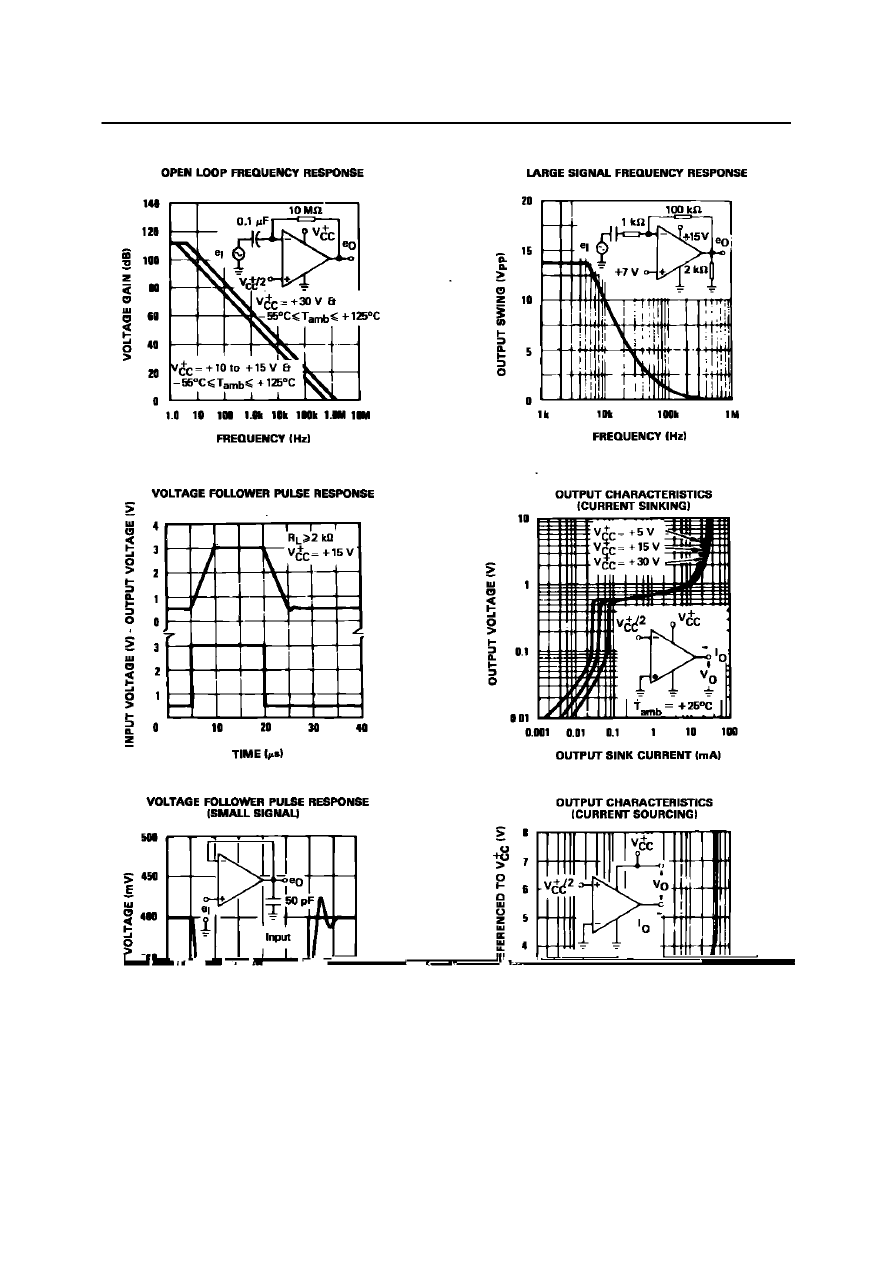
2902-03.EPS
2902-04.EPS
2902-05.EPS
2902-06.EPS
2902-07.EPS
2902-08.EPS
LM2902
5/11
2902-09.EPS
LM2902
6/11
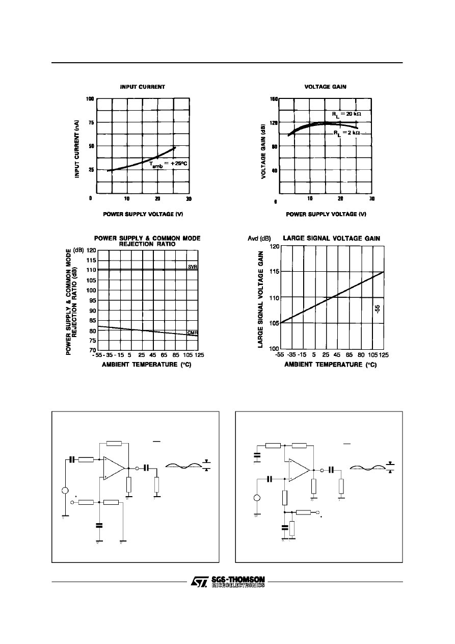
2902-10.EPS
2902-11.EPS
2902-12.EPS
2902-13.EPS
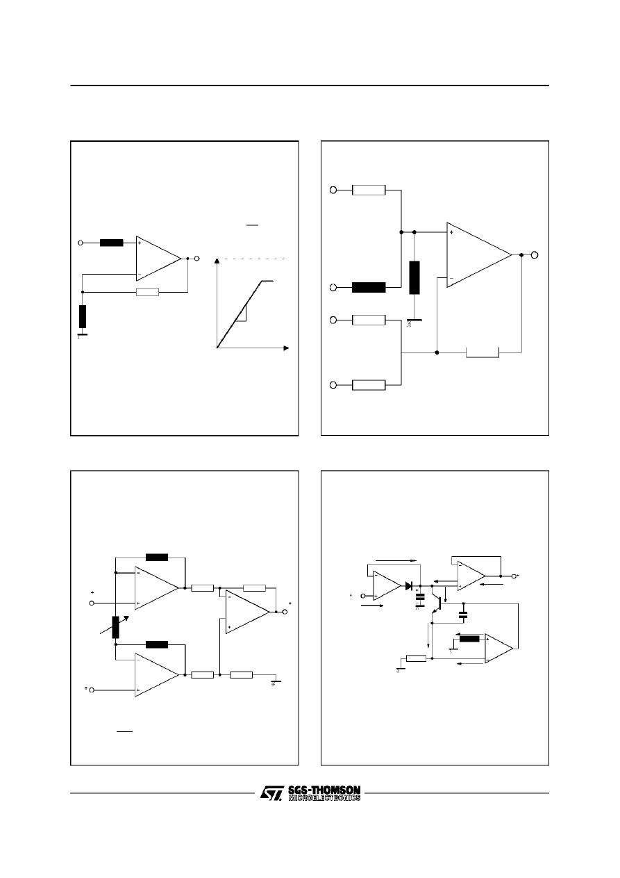
TYPICAL SINGLE - SUPPLY APPLICATIONS
1/4
LM2902
~
0
2V
PP
R
10k
Ω
L
C
o
e
o
R
6.2k
Ω
B
R
100k
Ω
f
R1
10k
Ω
C
I
e
I
V
CC
R2
100k
Ω
C1
10
µ
F
R3
100k
Ω
A =-
R
R1
V
f
(as shown A =-10)
V
2902-14.EPS
AC COUPLED INVERTING AMPLIFIER
~
0
2V
PP
R
10k
Ω
L
C
o
e
o
R
6.2k
Ω
B
C1
0.1
µ
F
e
I
V
CC
(asshown A =11)
V
A =1 +R2
R1
V
R1
100k
Ω
R2
1M
Ω
C
I
R3
1M
Ω
R4
100k
Ω
R5
100k
Ω
C2
10
µ
F
1/4
LM2902
2902-15.EPS
AC COUPLED NON-INVERTING AMPLIFIER
LM2902
7/11
R1
10k
Ω
R2
1M
Ω
1/4
LM2902
10k
Ω
e
I
e
O
+5V
e
O
(V)
(mV)
0
A
V
=1 + R2
R1
(Asshown
= 101)
A
V
2902-16.EPS
NON-INVERTING DC GAIN
1/4
LM2902
e
O
e
4
e
3
e
2
e
1
100k
Ω
100k
Ω
100k
Ω
100k
Ω
100k
Ω
100k
Ω
2902-17.EPS
e
o
= e
1
+ e
2
- e
3
- e
4
where (e
1
+ e
2
)
≥
(e
3
+ e
4
)
to keep e
o
≥
0V
DC SUMMING AMPLIFIER
1/4
LM2902
R3
100k
Ω
e
O
1/4
LM2902
R1
100k
Ω
e
1
1/4
LM2902
R7
100k
Ω
R6
100k
Ω
R5
100k
Ω
e
2
R2
2k
Ω
Gainadjust
R4
100k
Ω
2902-18.EPS
if R
1
= R
5
and R
3
= R
4
= R
6
= R
7
e
o
=
[ 1
+
2R
1
R
2
]
(
e
2
−
e
1
)
As shown e
o
= 101 (e
2
- e
1
).
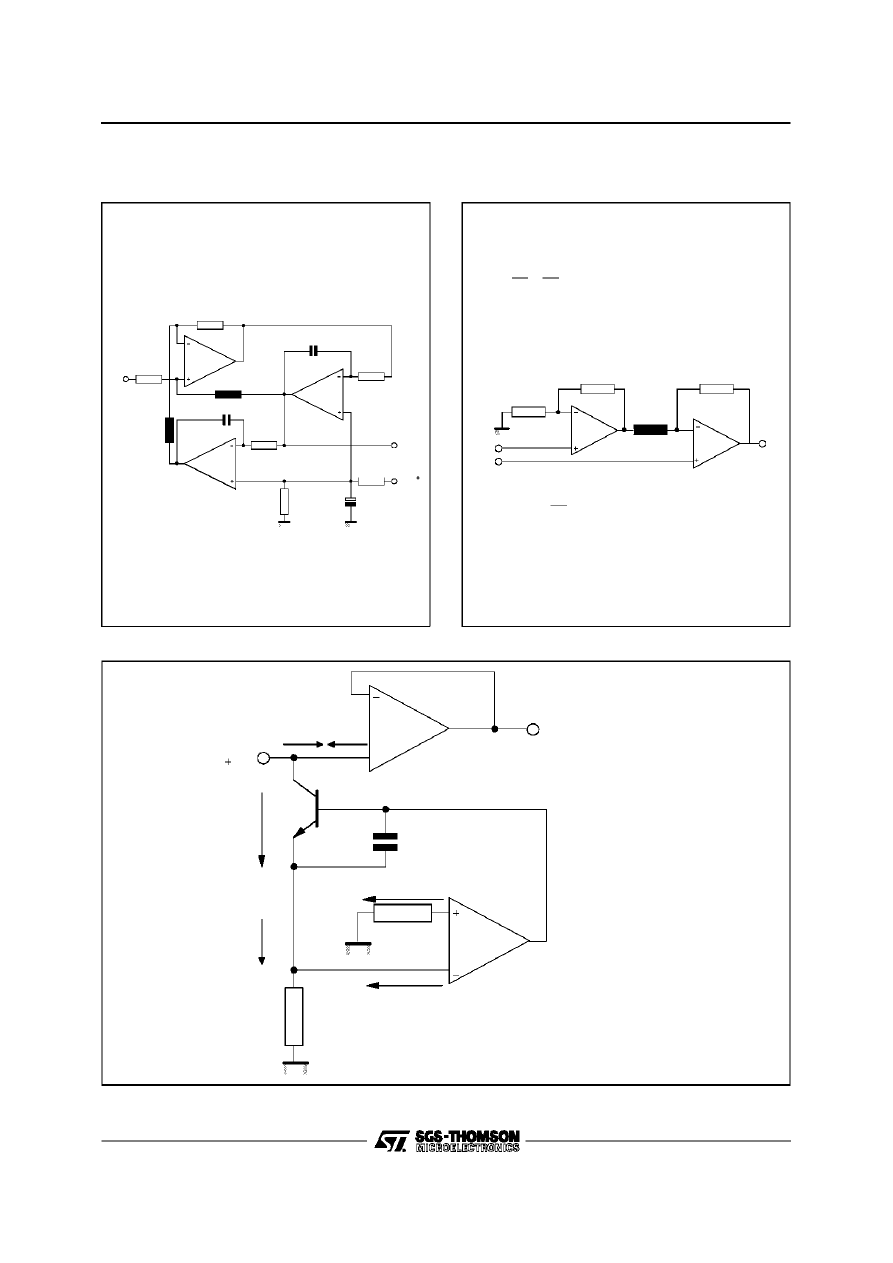
HIGH INPUT Z ADJUSTABLE GAIN DC
INSTRUMENTATION AMPLIFIER
TYPICAL SINGLE - SUPPLY APPLICATIONS
1/4
LM2902
I
B
2N929
0.001
µ
F
I
B
3R
3M
Ω
I
B
Input current
compensation
e
o
I
B
e
I
Z
o
Z
I
C
1
µ
F
2I
B
R
1M
Ω
2I
B
* Polycarbonate or polyethylene
*
1/4
LM2902
1/4
LM2902
2902-19.EPS
LOW DRIFT PEAK DETECTOR
LM2902
8/11
1/4
LM2902
1/4
LM2902
R3
10k
Ω
1/4
LM2902
e
1
e
O
R8
100k
Ω
R7
100k
Ω
C3
10
µ
F
V
CC
R5
470k
Ω
C2
330pF
R4
10M
Ω
R6
470k
Ω
R1
100k
Ω
C1
330pF
2902-20.EPS
F
O
= 1kHz
Q = 50
A
V
= 100 (40dB)
ACTIVER BANDPASS FILTER
1/4
LM2902
R1
100k
Ω
R2
100k
Ω
R4
100k
Ω
R3
100k
Ω
+V2
+V1
V
o
1/4
LM2902
2902-21.EPS
e
o
(
1
+
R
4
R
3
) (
e
2
−
e
1
)
As shown e
o
= (e
2
- e
1
)
For
R
1
R
2
=
R
4
R
3
(CMRR depends on this resistor ratio match)
HIGH INPUT Z, DC DIFFERENTIAL AMPLIFIER
1/4
LM2902
I
B
2N929
0.001
µ
F
I
B
3M
Ω
I
B
e
o
I
I
e
I
I
B
I
B
Aux. amplifier for input
current compensation
1.5M
Ω
1/4
LM2902
2902-22.EPS
USING SYMMETRICAL AMPLIFIERS TO REDUCE INPUT CURRENT (GENERAL CONCEPT)
TYPICAL SINGLE - SUPPLY APPLICATIONS
LM2902
9/11
PM-DIP14.EPS
PACKAGE MECHANICAL DATA
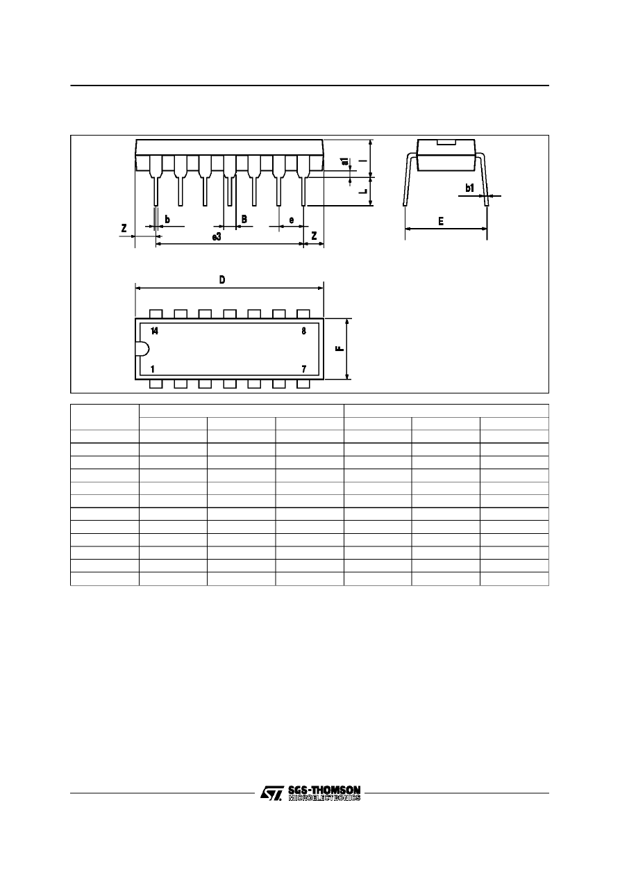
14 PINS - PL ASTIC DIP OR CERDIP
Dimensions
Millimeters
Inches
Min.
Typ.
Max.
Min.
Typ.
Max.
a1
0.51
0.020
B
1.39
1.65
0.055
0.065
b
0.5
0.020
b1
0.25
0.010
D
20
0.787
E
8.5
0.335
e
2.54
0.100
e3
15.24
0.600
F
7.1
0.280
i
5.1
0.201
L
3.3
0.130
Z
1.27
2.54
0.050
0.100
DIP14.TBL
LM2902
10/11
PM-SO14.EPS
PACKAGE MECHANICAL DATA
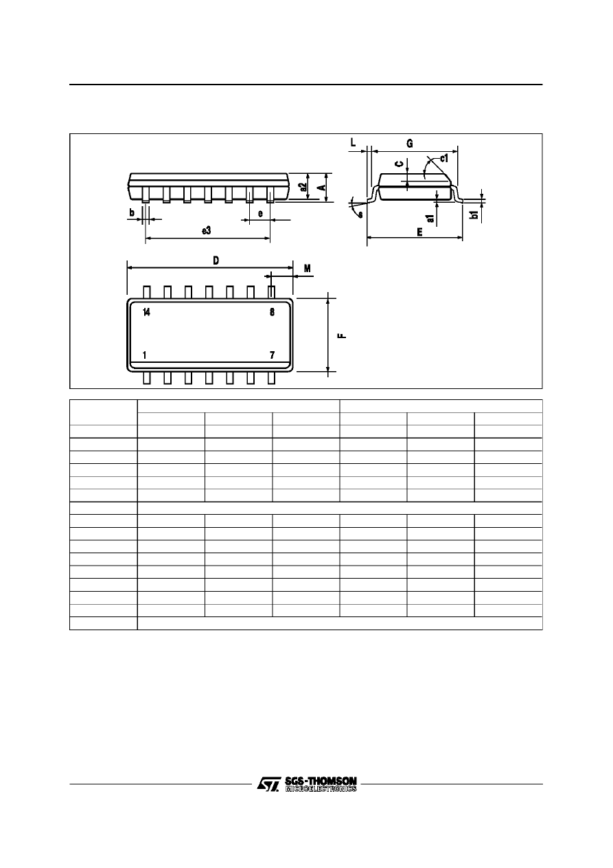
14 PINS - PL ASTIC MICROPACKAGE (SO)
Dimensions
Millimeters
Inches
Min.
Typ.
Max.
Min.
Typ.
Max.
A
1.75
0.069
a1
0.1
0.2
0.004
0.008
a2
1.6
0.063
b
0.35
0.46
0.014
0.018
b1
0.19
0.25
0.007
0.010
C
0.5
0.020
c1
45
o
(typ.)
D
8.55
8.75
0.336
0.334
E
5.8
6.2
0.228
0.244
e
1.27
0.050
e3
7.62
0.300
F
3.8
4.0
0.150
0.157
G
4.6
5.3
0.181
0.208
L
0.5
1.27
0.020
0.050
M
0.68
0.027
S
8
o
(max.)
SO14.TBL
Information furnished is believed to be accurate and reliable. However, SGS-THOMSON Microelectronics assumes no responsi-
bility for the consequences of use of such information nor for any infringement of patents or other rights of third parties which
may result from its use. No licence is granted by implication or otherwise under any patent or patent rights of SGS-THOMSON
Microelectronics. Specifications mentioned in this publication are subject to change without noti ce. This publ ication supersedes
and replaces all information previously supplied. SGS-THOMSON Microelectronics products are not authorized for use as critical
componen ts in life support devices or systems without express written approval of SGS-THOMSON Microelectronics.
1995 SGS-THOMSON Microelectronics - All Rights Reserved
SGS-THOMSON Microelectronics GROUP OF COMPANIES
Australia - Brazil - France - Germany - Hong Kong - Italy - Japan - Korea - Malaysia - Malta - Morocco - The Netherlands
Singapore - Spain - Sweden - Switzerland - Taiwan - Thailand - United Kingdom - U.S.A.
ORDER
CODE
:
LM2902
11/11
Wyszukiwarka
Podobne podstrony:
LM224 LM324 LM2902
LM2902
więcej podobnych podstron