1
LT1117/LT1117-2.85
LT1117-3.3/LT1117-5
800mA Low Dropout
Positive Regulators
Adjustable and Fixed 2.85V,
3.3V, 5V
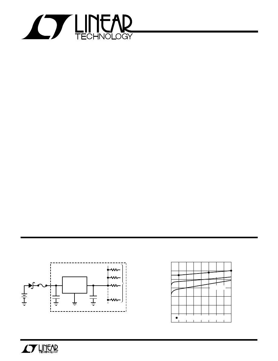
Active Terminator for SCSI-2 Bus
Dropout Voltage (V
IN
– V
OUT
)
U
A
O
PPLICATI
TYPICAL
D
U
ESCRIPTIO
S
FEATURE
■
Space Saving SOT-223 Surface Mount Package
■
Three-Terminal Adjustable or Fixed 2.85V, 3.3V, 5V
■
Output Current of 800mA
■
Operates Down to 1V Dropout
■
Guaranteed Dropout Voltage at Multiple Current Levels
■
0.2% Line Regulation Max
■
0.4% Load Regulation Max
The LT1117 is a positive low dropout regulator designed
to provide up to 800mA of output current. The device is
available in an adjustable version and fixed output voltages
of 2.85V, 3.3V and 5V. The 2.85V version is designed
specifically to be used in Active Terminators for the SCSI
bus. All internal circuitry is designed to operate down to 1V
input to output differential. Dropout voltage is guaranteed
at a maximum of 1.2V at 800mA, decreasing at lower load
currents. On chip trimming adjusts the reference/output
voltage to within
±
1%. Current limit is also trimmed in
order to minimize the stress on both the regulator and the
power source circuitry under overload conditions.
The low profile surface mount SOT-223 package allows
the device to be used in applications where space is
limited. The LT1117 requires a minimum of 10
µ
F of output
capacitance for stability. Output capacitors of this size or
larger are normally included in most regulator designs.
Unlike PNP type regulators where up to 10% of the output
current is wasted as quiescent current, the quiescent
current of the LT1117 flows into the load, increasing
efficiency.
U
S
A
O
PPLICATI
■
Active SCSI Terminators
■
High Efficiency Linear Regulators
■
Post Regulators for Switching Supplies
■
Battery Chargers
■
5V to 3.3V Linear Regulators
18 TO 27
LINES
LT1117 • TA01
+
+
10
µ
F
110
Ω
110
Ω
110
Ω
110
Ω
4.75V TO
5.25V
22
µ
F
LT1117-2.85
IN
GND
OUT
OUTPUT CURRENT (mA)
0
0
DROPOUT VOLTAGE (V)
0.2
0.4
0.6
0.8
1.0
1.4
100
400
600
800
LT1117 • TPC01
1.2
200 300
500
700
T
J
= 25
°
C
T
J
= 125
°
C
INDICATES GUARANTEED TEST POINT
2
LT1117/LT1117-2.85
LT1117-3.3/LT1117-5
A
U
G
W
A
W
U
W
A
R
BSOLUTE
XI
TI
S
Input Voltage
Operating Voltage
LT1117, LT1117-3.3, LT1117-5 ...................... 15V
LT1117-2.85 ................................................... 10V
Surge Voltage
LT1117, LT1117-3.3, LT1117-5 ...................... 20V
W
U
U
PACKAGE/ORDER I FOR ATIO
ORDER PART
NUMBER
LT1117CST
LT1117CST-2.85
LT1117CST-3.3
LT1117CST-5
PART MARKING
ORDER PART
NUMBER
LT1117CM
LT1117CM-2.85
LT1117CM-3.3
LT1117CM-5
PART MARKING
PARAMETER
CONDITIONS
MIN
TYP
MAX
UNITS
Reference Voltage
LT1117
I
OUT
= 10mA, (V
IN
– V
OUT
) = 2V, T
J
= 25
°
C
1.238
1.250
1.262
V
10
≤
I
OUT
≤
800mA, 1.4V
≤
(V
IN
- V
OUT
)
≤
10V
●
1.225
1.250
1.270
V
Output Voltage
LT1117-2.85
I
OUT
= 10mA, V
IN
= 4.85V, T
J
= 25
°
C
2.820
2.850
2.880
V
0
≤
I
OUT
≤
800mA, 4.25V
≤
V
IN
≤
10V
●
2.790
2.850
2.910
V
0
≤
I
OUT
≤
500mA, V
IN
= 3.95V
●
2.790
2.850
2.910
V
LT1117-3.3
I
OUT
= 10mA, V
IN
= 5V, T
J
= 25
°
C
3.267
3.300
3.333
V
0
≤
I
OUT
≤
800mA, 4.75V
≤
V
IN
≤
10V
●
3.235
3.300
3.365
V
LT1117-5
I
OUT
= 10mA, V
IN
= 7V, T
J
= 25
°
C
4.950
5.000
5.050
V
0
≤
I
OUT
≤
800mA, 6.50V
≤
V
IN
≤
12V
●
4.900
5.000
5.100
V
Line Regulation
LT1117
I
OUT
= 10mA, 1.5V
≤
V
IN
– V
OUT
≤
15V (Note 1)
●
0.035
0.2
%
LT1117-2.85
I
OUT
= 0mA, 4.25V
≤
V
IN
≤
10V (Note 1)
●
1
6
mV
LT1117-3.3
I
OUT
= 0mA, 4.75V
≤
V
IN
≤
15V (Note 1)
●
1
6
mV
LT1117-5
I
OUT
= 0mA, 6.5V
≤
V
IN
≤
15V (Note 1)
●
1
10
mV
Load Regulation
LT1117
(V
IN
– V
OUT
) = 3V, 10mA
≤
I
OUT
≤
800mA (Note 1)
●
0.1
0.4
%
LT1117-2.85
V
IN
= 4.25V, 0
≤
I
OUT
≤
800mA (Note 1)
●
1
10
mV
LT1117-3.3
V
IN
= 4.75V, 0
≤
I
OUT
≤
800mA (Note 1)
●
1
10
mV
LT1117-5
V
IN
= 6.5V, 0
≤
I
OUT
≤
800mA (Note 1)
●
1
15
mV
Dropout Voltage
I
OUT
= 100mA (Note 2)
●
1.00
1.10
V
I
OUT
= 500mA (Note 2)
●
1.05
1.15
V
I
OUT
= 800mA (Note 2)
●
1.10
1.20
V
Current Limit
(V
IN
– V
OUT
) = 5V, T
J
= 25
°
C,
800
950
1200
mA
Minimum Load Current
LT1117
(V
IN
– V
OUT
) = 15V (Note 3)
●
1.7
5
mA
ELECTRICAL C
C
HARA TERISTICS
Operating JunctionTemperature Range ..... 0
°
C to 125
°
C
Storage Temperature Range ................. – 65
°
C to 150
°
C
Lead Temperature ................... (See Soldering Methods)
T
J MAX
= 125
°
C,
θ
JC
= 15
°
C/W
FRONT VIEW
TAB IS
V
OUT
IN
OUT
ADJ/GND
ST PACKAGE
3-LEAD PLASTIC SOT-223
3
2
1
M PACKAGE
3-LEAD PLASTIC DD
FRONT VIEW
3
2
1
IN
OUT
ADJ/GND
TAB IS
V
OUT
T
J MAX
= 125
°
C,
θ
JC
= 10
°
C/W
11173
11175
1117
11172
11173
11175
1117
11172
Consult factory for Industrial and Military grade parts.
3
LT1117/LT1117-2.85
LT1117-3.3/LT1117-5
PARAMETER
CONDITIONS
MIN
TYP
MAX
UNITS
Quiescent Current
LT1117-2.85
V
IN
≤
10V
●
5
10
mA
LT1117-3.3
V
IN
≤
15V
●
5
10
mA
LT1117-5
V
IN
≤
15V
●
5
10
mA
Thermal Regulation
T
A
= 25
°
C, 30ms Pulse
0.01
0.1
%/W
Ripple Rejection
f
RIPPLE
= 120Hz, (V
IN
– V
OUT
) = 3V,
V
RIPPLE
= 1Vp-p
●
60
75
dB
Adjust Pin Current
●
55
120
µ
A
Adjust Pin Current Change
10mA
≤
I
OUT
≤
800mA, 1.4V
≤
(V
IN
– V
OUT
)
≤
10V
●
0.2
5
µ
A
Temperature Stability
0.5
%
Long Term Stability
T
A
= 125
°
C, 1000Hrs
0.3
%
RMS Output Noise
(% of V
OUT
), 10Hz
≤
f
≤
10kHz
0.003
%
Thermal Resistance
(Junction-to-Case, at Tab)
15
°
C/W
ELECTRICAL C
C
HARA TERISTICS
The
●
denotes specifications which apply over the full operating
temperature range.
Note 1: See thermal regulation specification for changes in output voltage
due to heating effects. Load regulation and line regulation are measured at
a constant junction temperature by low duty cycle pulse testing.
Note 2: Dropout voltage is specified over the full output current range of
the device. Dropout voltage is defined as the minimum input/output
differential measured at the specified output current. Test points and limits
are also shown on the Dropout Voltage curve.
Note 3: Minimum load current is defined as the minimum output current
required to maintain regulation.
C
C
HARA TERISTICS
U
W
A
TYPICAL PERFOR
CE
Minimum Operating Current
(Adjustable Device)
Short-Circuit Current
Load Regulation
INPUT/OUTPUT DIFFERENTIAL (V)
0
0
MINIMUM OPERATING CURRENT (mA)
1
3
4
10
15
20
LT1117 • TPC02
5
T
J
= 25
°
C
T
J
= 125
°
C
T
J
= –55
°
C
2
INPUT/OUTPUT DIFFERENTIAL (V)
0
0
SHORT CIRCUIT CURRENT (A) 0.25
0.50
0.75
1.25
10
15
LT1117 • TPC03
5
1.00
T
J
= 25
°
C
T
J
= 125
°
C
TEMPERATURE (
°
C)
–50
– 0.20
OUTPUT VOLTAGE DEVIATION (%) – 0.15
– 0.10
– 0.05
0.10
50
75
125
LT1117 • TPC04
0
0.05
0
–25
25
100
∆
I
LOAD
= 800mA
4
LT1117/LT1117-2.85
LT1117-3.3/LT1117-5
C
C
HARA TERISTICS
U
W
A
TYPICAL PERFOR
CE
LT1117-5
Line Transient Response
LT1117-2.8
Line Transient Response
LT1117 Ripple Rejection
LT1117 Ripple Rejection vs Current
Temperature Stability
LT1117-2.85
LT1117-5
Adjust Pin Current
Load Transient Response
Load Transient Response
TEMPERATURE (
°
C)
–50
–2.0
OUTPUT VOLTAGE CHANGE (%)
–1.0
0
2.0
0
50
100
150
LT1117 • TPC07
1.0
–25
25
75
125
TEMPERATURE (
°
C)
–50
0
AJUST PIN CURRENT (
µ
A)
20
50
100
0
50
100
150
LT1117 • TPC08
80
–25
25
75
125
10
30
40
60
70
90
FREQUENCY (Hz)
20
RIPPLE REJECTION (dB)
40
60
80
100
10
1k
10k
100k
LT1117 • TPC05
0
100
90
70
50
30
10
C
ADJ
= 200
µ
F AT f < 60Hz
C
ADJ
= 25
µ
F AT f > 60Hz
I
OUT
= 0.5A
(V
IN
– V
OUT)
≥
V
DROPOUT
V
RIPPLE
≤
3V
P-P
V
RIPPLE
≤
0.5V
P-P
(V
IN
– V
OUT)
≥
3V
TIME (
µ
s)
0
– 0.5
LOAD CURRENT
(A)
0.3
20
50
70
100
LT1117 • TPC09
0.1
10
30
60
80
0
0.5
– 0.2
0
0.2
– 0.1
40
90
OUPUT VOLTAGE
DEVIATION (V)
C
IN
= 10
µ
F
C
OUT
= 10
µ
F TANTALUM
V
IN
= 4.25V
PRELOAD = 0.1A
TIME (
µ
s)
0
– 0.5
LOAD CURRENT
(A)
0.3
20
50
70
100
LT1117 • TPC10
0.1
10
30
60
80
0
0.5
– 0.2
0
0.2
– 0.1
40
90
OUPUT VOLTAGE
DEVIATION (V)
C
IN
= 10
µ
F
C
OUT
= 10
µ
F TANTALUM
V
IN
= 6.5V
PRELOAD = 0.1A
TIME (
µ
s)
0
3.25
INPUT VOLTAGE
(V)
60
40
100
140
200
LT1117 • TPC11
20
20
60
120
160
4.25
5.25
–40
0
40
–20
80
180
OUPUT VOLTAGE
DEVIATION (mV)
C
IN
= 1
µ
F
C
OUT
= 10
µ
F TANTALUM
I
OUT
= 0.1A
TIME (
µ
s)
0
5.50
INPUT VOLTAGE
(V)
60
40
100
140
200
LT1117 • TPC12
20
20
60
120
160
6.50
7.50
–40
0
40
–20
80
180
OUPUT VOLTAGE
DEVIATION (mV)
C
IN
= 1
µ
F
C
OUT
= 10
µ
F TANTALUM
I
OUT
= 0.1A
OUTPUT CURRENT (A)
0
0
RIPPLE REJECTION (dB)
20
30
50
80
100
0.2
0.4
0.6
0.8
LT1117 • TPC06
10
40
60
70
90
V
OUT
= 5V
C
ADJ
= 25
µ
F
C
OUT
= 25
µ
F
V
RIPPLE
≤
3V
P-P
f
RIPPLE
=
120Hz
f
RIPPLE
=
20kHz
V
RIPPLE
≤
0.5V
P-P
5
LT1117/LT1117-2.85
LT1117-3.3/LT1117-5
W
I
D AGRA
BLOCK
U
A
O
PPLICATI
HI
U
TS
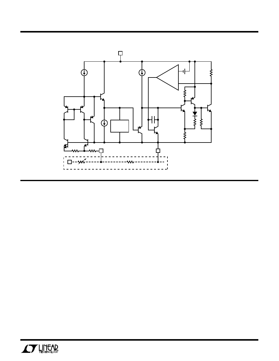
The LT1117 family of three-terminal regulators are easy to
use. They are protected against short circuit and thermal
overloads. Thermal protection circuitry will shutdown the
regulator should the junction temperature exceed 165
°
C
at the sense point. These regulators are pin compatible
with older three-terminal adjustable regulators, offer
lower dropout voltage and more precise reference toler-
ance. Reference stability over temperature is improved
over older types of regulators.
Stability
The LT1117 family of regulators requires an output ca-
pacitor as part of the device frequency compensation. A
minimum of 10
µ
F of tantalum or 50
µ
F of aluminum
electrolytic is required. The ESR of the output capacitor
should be less than 0.5
Ω
. Surface mount tantalum capaci-
tors, which have very low ESR, are available from several
manufacturers.
When using the LT1117 adjustable device the adjust
terminal can be bypassed to improve ripple rejection.
When the adjust terminal is bypassed the required value
of the output capacitor increases. The device will require
an output capacitor of 22
µ
F tantalum or 150
µ
F aluminum
electrolytic when the adjust pin is bypassed.
Normally, capacitor values on the order of 100
µ
F are used
in the output of many regulators to ensure good load
transient response with large load current changes. Out-
put capacitance can be increased without limit and larger
values of output capacitance further improve stability and
transient response.
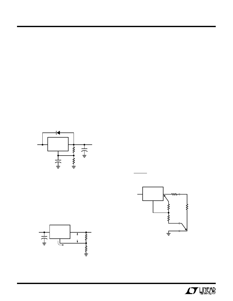
Protection Diodes
In normal operation, the LT1117 family does not need any
protection diodes. Older adjustable regulators required
protection diodes between the adjust pin and the output
and between the output and input to prevent over stress-
ing the die. The internal current paths on the LT1117 adjust
pin are limited by internal resistors. Therefore, even with
capacitors on the adjust pin, no protection diode is needed
to ensure device safety under short circuit conditions. The
LT1117 • BD01
–
+
THERMAL
LIMIT
OUT
IN
ADJ
GND
FOR FIXED VOLTAGE DEVICE
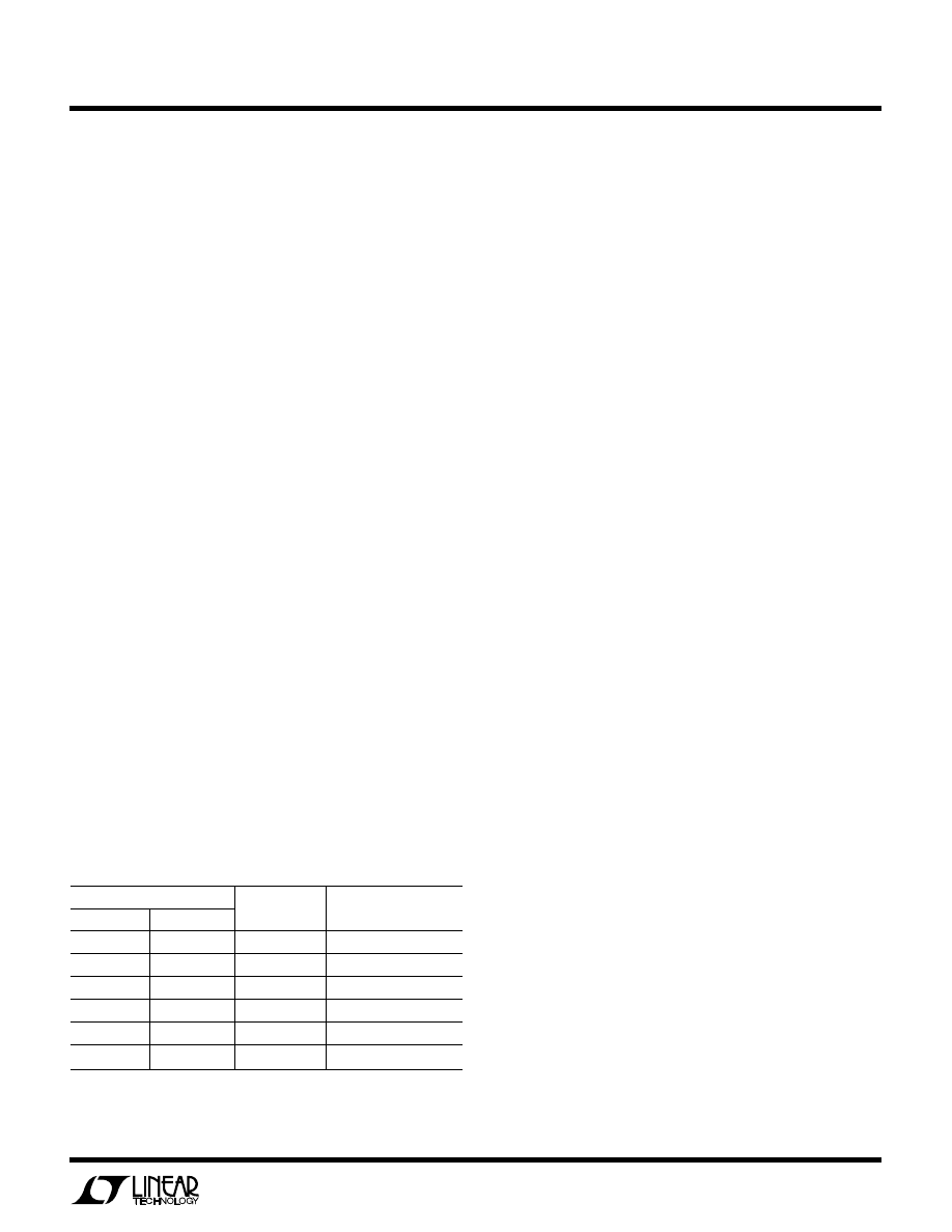
6
LT1117/LT1117-2.85
LT1117-3.3/LT1117-5
U
A
O
PPLICATI
HI
U
TS
adjust pin can be driven, on a transient basis,
±
25V with
respect to the output without any device degradation.
Diodes between input and output are not usually needed.
The internal diode between the output and input pins of the
device can withstand microsecond surge currents of 10A
to 20A. Normal power supply cycling can not generate
currents of this magnitude. Only with extremely large
output capacitors, such as 1000
µ
F and larger, and with the
input pin instantaneously shorted to ground can damage
occur. A crowbar circuit at the input of the LT1117 in
combination with a large output capacitor could generate
currents large enough to cause damage. In this case a
diode from output to input is recommended, as shown in
Figure 1.
to set the overall output voltage. Normally this current is
chosen to be the specified minimum load current of 10mA.
Because I
ADJ
is very small and constant when compared
to the current through R1, it represents a small error and
can usually be ignored. For fixed voltage devices R1 and
R2 are included in the device.
Load Regulation
Because the LT1117 is a three-terminal device, it is not
possible to provide true remote load sensing. Load regu-
lation will be limited by the resistance of the wire connect-
ing the regulator to the load. The data sheet specification
for load regulation is measured at the output pin of the
device. Negative side sensing is a true Kelvin connection,
with the bottom of the output divider returned to the
negative side of the load. Although it may not be immedi-
ately obvious, best load regulation is obtained when the
top of the resistor divider (R1) is returned directly to the
output pin of the device, not to the load. This is illustrated
in Figure 3. Connected as shown, R
P
is not multiplied by
the divider ratio. If R1 were connected to the load, the
effective resistance between the regulator and the load
would be:
Figure 3. Connections for Best Load Regulation
For fixed voltage devices the top of R1 is internally Kelvin
connected, and the ground pin can be used for negative
side sensing.
R
R
R
R
R
P
P
×
+
=
2
1
1
,
Parasitic Line Resistance
LT1117 • TA02
+
+
D1
1N4002
(OPTIONAL)
C
ADJ
10
µ
F
R2
R1
C
OUT
150
µ
F
V
OUT
V
IN
LT1117
IN
ADJ
OUT
LT1117 • TA04
R2
R1
V
IN
R
P
PARASITIC
LINE RESISTANCE
R
L
CONNECT
R1 TO CASE
CONNECT
R2 TO LOAD
LT1117
IN
ADJ
OUT
Figure 2. Basic Adjustable Regulator
LT1117 • TA03
R2
R1
V
OUT
V
IN
V
REF
I
ADJ
50
µ
A
LT1117
IN
ADJ
OUT
V
OUT
= V
REF
1 + + I
ADJ
R2
R2
—
R1
( )
Output Voltage
The LT1117 develops a 1.25V reference voltage between
the output and the adjust terminal (see Figure 2). By
placing a resistor between these two terminals, a constant
current is caused to flow through R1 and down through R2
Figure 1.
7
LT1117/LT1117-2.85
LT1117-3.3/LT1117-5
Thermal Considerations
LT1117 series regulators have internal thermal limiting
circuitry designed to protect the device during overload
conditions. For continuous normal load conditions how-
ever, the maximum junction temperature rating of 125
°
C
must not be exceeded.
It is important to give careful consideration to all sources
of thermal resistance from junction to ambient. For the
SOT-223 package, which is designed to be surface
mounted, additional heat sources mounted near the de-
vice must also be considered. Heat sinking is accom-
plished using the heat spreading capability of the PC board
and its copper traces. The thermal resistance of the
LT1117 is 15
°
C/W from the junction to the tab. Thermal
resistances from tab to ambient can be as low as 30
°
C/W.
The total thermal resistance from junction to ambient can
be as low as 45
°
C/W. This requires a reasonable sized PC
board with at least one layer of copper to spread the heat
across the board and couple it into the surrounding air.
Experiments have shown that the heat spreading copper
layer does not need to be electrically connected to the tab
of the device. The PC material can be very effective at
transmitting heat between the pad area, attached to the tab
of the device, and a ground plane layer either inside or on
the opposite side of the board. Although the actual thermal
resistance of the PC material is high, the Length/Area ratio
of the thermal resistor between layers is small. The data in
Table 1 was taken using 1/16" FR-4 board with 1oz. copper
foil. It can be used as a rough guideline in estimating
thermal resistance.
Table 1.
COPPER AREA
THERMAL RESISTANCE
TOPSIDE*
BACKSIDE
BOARD AREA
(JUNCTION-TO-AMBIENT)
2500 Sq. mm
2500 Sq. mm
2500 Sq. mm
45
°
C/W
1000 Sq. mm
2500 Sq. mm
2500 Sq. mm
45
°
C/W
225 Sq. mm
2500 Sq. mm
2500 Sq. mm
53
°
C/W
100 Sq. mm
2500 Sq. mm
2500 Sq. mm
59
°
C/W
1000 Sq. mm
1000 Sq. mm
1000 Sq. mm
52
°
C/W
1000 Sq. mm
0
1000 Sq. mm
55
°
C/W
* Tab of device attached to topside copper
U
A
O
PPLICATI
HI
U
TS
The thermal resistance for each application will be affected
by thermal interactions with other components on the
board. Some experimentation will be necessary to deter-
mine the actual value.
The power dissipation of the LT1117 is equal to:
P
D
= ( V
IN
– V
OUT
)( I
OUT
)
Maximum junction temperature will be equal to:
T
J
= T
A(MAX)
+ P
D
(Thermal Resistance (junction-to-
ambient))
Maximum junction temperature must not exceed 125
°
C.
Ripple Rejection
The curves for Ripple Rejection were generated using an
adjustable device with the adjust pin bypassed. These
curves will hold true for all values of output voltage. For
proper bypassing, and ripple rejection approaching the
values shown, the impedance of the adjust pin capacitor,
at the ripple frequency, should be < R1. R1 is normally in
the range of 100
Ω
-200
Ω
. The size of the required adjust
pin capacitor is a function of the input ripple frequency. At
120Hz, with R1=100
Ω
, the adjust pin capacitor should be
> 13
µ
F. At 10kHz only 0.16
µ
F is needed.
For fixed voltage devices, and adjustable devices without
an adjust pin capacitor, the output ripple will increase as
the ratio of the output voltage to the reference voltage
(V
OUT
/ V
REF
). For example, with the output voltage equal to
5V, the output ripple will be increased by the ratio of 5V/
1.25V. It will increase by a factor of four. Ripple rejection
will be degraded by 12dB from the value shown
on the curve.
8
LT1117/LT1117-2.85
LT1117-3.3/LT1117-5
U
S
A
O
PPLICATI
TYPICAL
1.2V to 10V Adjustable Regulator
5V Regulator with Shutdown
Remote Sensing
Adjusting Output Voltage of Fixed Regulators
Regulator with Reference
LT1117 • TA05
+
R1
121
Ω
C2
100
µ
F
V
OUT
†
V
IN
V
OUT
= 1.25V 1 +
R2
—
R1
+
C1*
10
µ
F
R2
1k
NEEDED IF DEVICE IS FAR FROM FILTER CAPACITORS
*
†
LT1117
IN
ADJ
OUT
( )
121
Ω
1%
100
µ
F
5V
V
IN
10
µ
F
365
Ω
1%
1k
1k
+
TTL
+
LT1117 • TA06
LT1117
IN
ADJ
OUT
2N3904
LT1117 • TA07
121
Ω
V
IN
R
P
(MAX. DROP 300mV)
+
+
10
µ
F
+
+
–
100
µ
F
365
Ω
100pF
5
µ
F
25
Ω
1k
25
Ω
V
IN
R
L
7
2
3
4
8
1
6
LM301A
OUTPUT
5V
RETURN
RETURN
LT1117
IN
ADJ
OUT
100
µ
F
5V TO 10V
V
IN
> 12V
10
µ
F
LT1117 • TA08
+
10
µ
F*
+
1k
+
* OPTIONAL IMPROVES RIPPLE REJECTION
LT1117-5
IN
GND
OUT
100
µ
F
10V
V
IN
> 11.5V
10
µ
F
LT1117 • TA09
+
5V
OUT
+
LT1029
LT1117-5
IN
GND
OUT
9
LT1117/LT1117-2.85
LT1117-3.3/LT1117-5
U
S
A
O
PPLICATI
TYPICAL
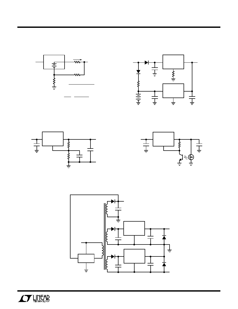
Battery Charger
Battery Backed Up Regulated Supply
Improving Ripple Rejection
Automatic Light Control
1.2k
10
µ
F
+
100
µ
F
LT1117 • TA16
LT1117
IN
ADJ
OUT
R1
121
Ω
1%
V
IN
≥
16.5V
V
IN
10
µ
F
C1
10
µ
F
150
µ
F
R2
365
Ω
1%
* C1 IMPROVES RIPPLE
REJECTION. X
C
SHOULD BE
≈
R1 AT RIPPLE FREQUENCY
LT1117 • TA14
+
+
LT1117
IN
ADJ
OUT
100
µ
F
5.2V LINE
5.0V BATTERY
V
IN
10
µ
F
LT1117 • TA13
+
50
Ω
+
+
SELECT FOR
CHARGE RATE
6.5V
10
µ
F
LT1117-5
IN
GND
OUT
LT1117-5
IN
GND
OUT
High Efficiency Dual Supply
+5V
0.5A
+V
IN
10
µ
F
LT1117 • TA12
1N4002
470
µ
F
10
µ
F
1N4002
470
µ
F
MUR410
MUR410
MUR410
SWITCHING
REGULATOR
470
µ
F
3.3V OUTPUT (TYPICAL)
–5V
0.5A
+
+
+
+
+
FEEDBACK PATH
LT1117-5
IN
GND
OUT
LT1117-5
IN
GND
OUT
LT1117 • TA10
V
OUT
V
IN
R1
IF
R
S
1.25V
ADJ
LT1117
IN
OUT
V
OUT
– 1.25V
1 +
R2
—
R1
IF =
–R
S
1 +
R2
—
R1
1
=
–R
S
1 +
R2
—
R1
( )
∆IF
∆V
OUT
( )
( )
10
LT1117/LT1117-2.85
LT1117-3.3/LT1117-5
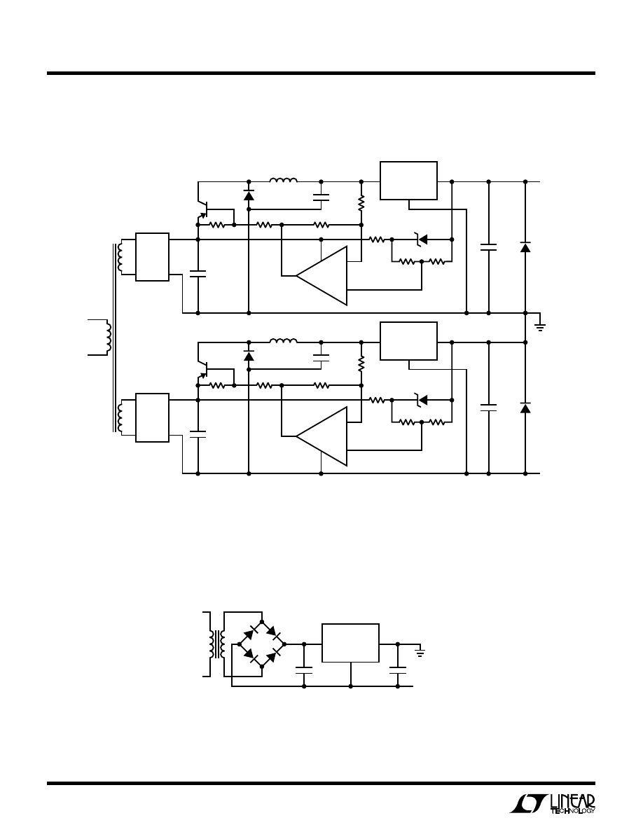
High Efficiency Dual Linear Supply
Low Dropout Negative Supply
U
S
A
O
PPLICATI
TYPICAL
100
µ
F
LT1117 • TA11
D2
1N4002
1000
µ
F
MBR360
–5V
0.5A
–
+
2.4k
510k
1k
30k
20k*
30.1k*
LT1004-2.5
10k
4700
µ
F
+
+
+
MDA201
+
–
(HEAT SINK)
2N6667
(DARLINGTON)
L1
285
µ
H
1/2
LT1018
100
µ
F
1000
µ
F
MBR360
–
+
2.4k
510k
1k
30k
20k*
30.1k*
LT1004-2.5
10k
4700
µ
F
+
+
+
MDA201
+
–
(HEAT SINK)
2N6667
(DARLINGTON)
L1
285
µ
H
1/2
LT1018
D11
1N4002
+5V
0.5A
STANCOR
P-8685
130VAC-
90VAC
*
MDA
L1
= 1 % FILM RESISTORS
= MOTOROLA
= PULSE ENGINEERING, INC. #PE-92106
V+
V–
LT1117-5
IN
GND
OUT
LT1117-5
IN
GND
OUT
Q1
100
µ
F
V
IN
LT1117 • TA17
+
V
OUT
= –5V
+
10
µ
F
FLOATING INPUT
LT1117-5
IN
GND
OUT
11
LT1117/LT1117-2.85
LT1117-3.3/LT1117-5
Information furnished by Linear Technology Corporation is believed to be accurate and reliable.
However, no responsibility is assumed for its use. Linear Technology Corporation makes no represen-
tation that the interconnection of its circuits as described herein will not infringe on existing patent rights.
U
S
A
O
PPLICATI
TYPICAL
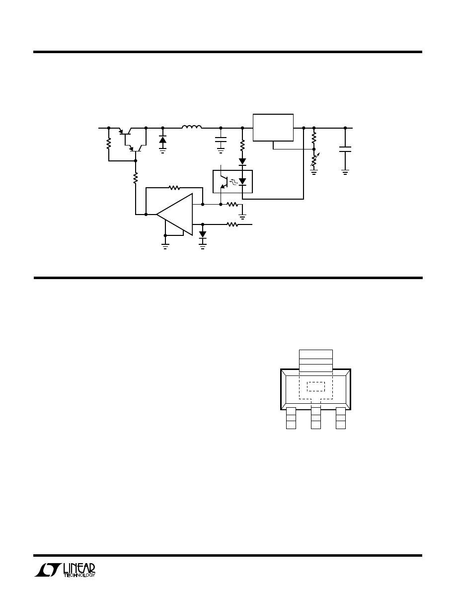
High Efficiency Regulator
LT1117 • TA18
U
W
ETHODS
SOLDERI G
The SOT-223 is manufactured with gull wing leadform for
surface mount applications. The leads and heatsink are
solder plated and allow easy soldering using non-active or
mildly active fluxes. The package is constructed with three
leads exiting one side of the package and one heatsink
exiting the other side, and the die attached to the heatsink
internally.
The recommended methods of soldering SOT-223 are:
vapor phase reflow and infrared reflow with preheat of
component to within 65
°
C of the solder temperature.
Hand soldering and wave soldering are not recom-
mended since these methods can easily damage the
part with excessive thermal gradients across the pack-
age.
Care must be exercised during surface mount to minimize
large (> 30
°
C per second) thermal shock to the package.
2k
OUTPUT
ADJUST
240
Ω
100
µ
F
+
470
Ω
1N914
4N28
–
+
1N914
1k
+
MR1122
10k
28V INPUT
1mH
10,000
µ
F
1M
10k
10k
LT1011
LT1117 • TA15
28V
OUTPUT
28V
LT1117
IN
ADJ
OUT
12
LT1117/LT1117-2.85
LT1117-3.3/LT1117-5
Linear Technology Corporation
1630 McCarthy Blvd., Milpitas, CA 95035-7487
(408) 432-1900
●
FAX
: (408) 434-0507
●
TELEX
: 499-3977
LINEAR TECHNOLOGY CORPORATION 1993
LT/GP 0993 5K REV B
U
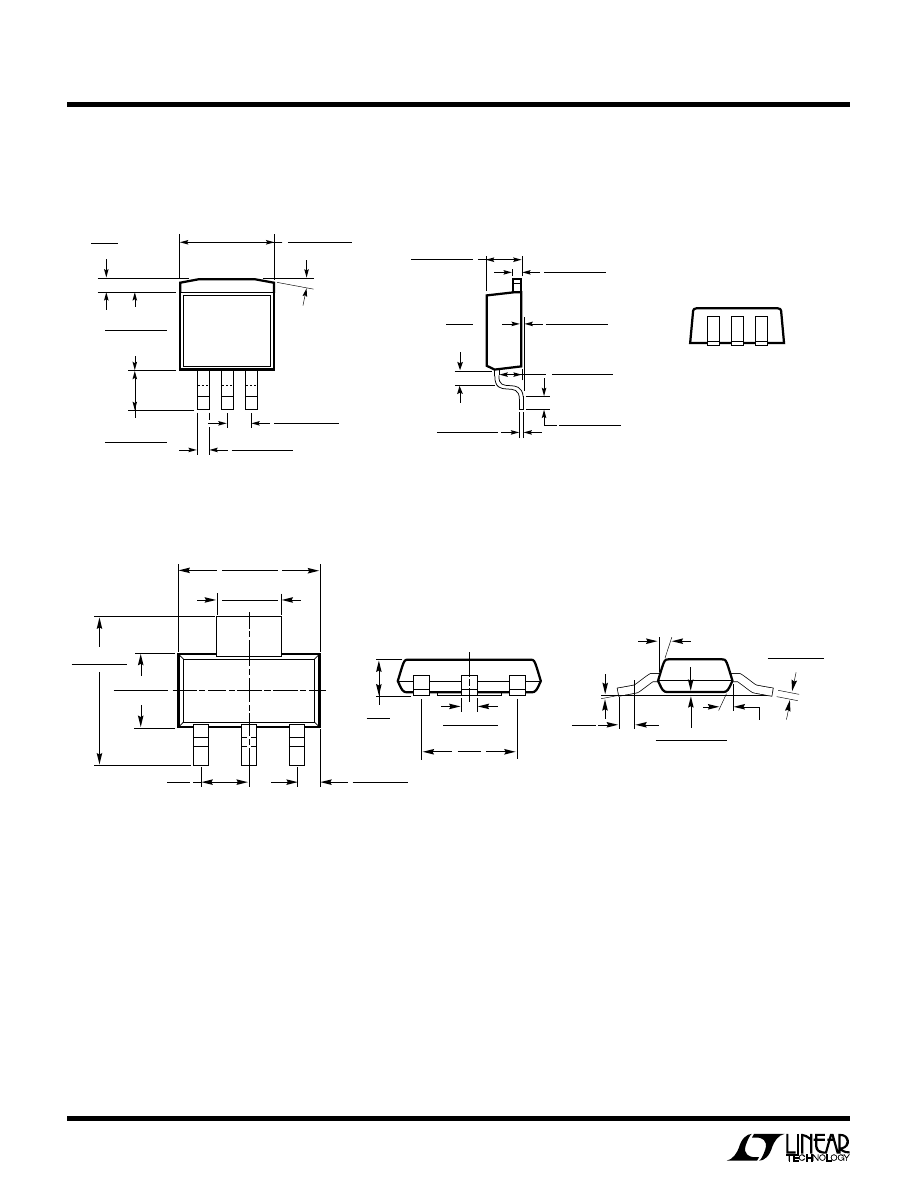
PACKAGE DESCRIPTIO
Dimensions in inches (millimeters) unless otherwise noted.
M Package
3-Lead Plastic DD
SOT233 0793
0.116 – 0.124
(2.95 – 3.15)
0.248 – 0.264
(6.30 – 6.71)
0.130 – 0.146
(3.30 – 3.71)
0.264 – 0.287
(6.71 – 7.29)
0.090
(2.29)
NOM
0.033 – 0.041
(0.84 – 1.04)
0.181
(4.60)
NOM
0.025 – 0.033
(0.64 – 0.84)
0.071
(1.80)
MAX
10°
MAX
0.012
(0.31)
MIN
0.0008 – 0.0040
(0.0203 – 0.1016)
10° – 16°
0.010 – 0.014
(0.25 – 0.36)
10° – 16°
DD3 0693
0.022 ± 0.005
(0.559 ± 0.127)
0.105 ± 0.008
(2.667 ± 0.203)
0.004
+0.008
–0.004
(
)
0.102
+0.203
–0.102
0.050 ± 0.012
(1.270 ± 0.305)
0.059
(1.499)
TYP
0.050 ± 0.008
(1.270 ± 0.203)
0.175 ± 0.008
(4.445 ± 0.203)
0.060
(1.524)
0.401 ± 0.015
(10.185 ± 0.381)
15° TYP
0.050 ± 0.008
(1.270 ± 0.203)
0.331
+0.012
–0.020
(
)
8.407
+0.305
–0.508
0.143
+0.012
–0.020
(
)
3.632
+0.305
–0.508
0.100 ± 0.010
(2.5402 ± 0.254)
ST Package
3-Lead Plastic SOT-223
Wyszukiwarka
Podobne podstrony:
Datasheet SL4 100
Datasheet QS10 241 C1
Datasheet YR2 DIODE
pdf datasheet 5 id 352824 Nieznany
Citroen C4 Picasso Datasheet
datasheet
Datasheet SL5 300
LBB441850 DataSheet plPL E3338100491
Datasheet ML15 051
Datasheet SL10 305
Datasheet SL20 303
PLN 1P1000 DataSheet plPL E3242294027
Datasheet QT20 241 C1
Datasheet SLR2 100
LBC308001 DataSheet plPL E2141295243
1830 switch datasheet
Datasheet SL30 100
Datasheet SL20 100
więcej podobnych podstron