Low-Voltage/Low-Power
Copyright © 2008 by Silicon Laboratories
1.14.2008
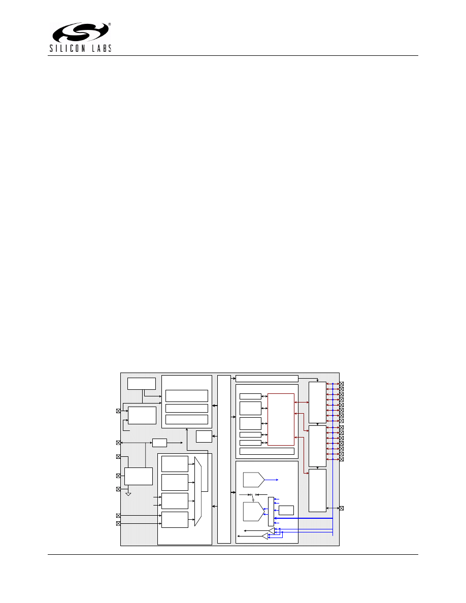
Port 0
Drivers
Digital Peripherals
UART
Timers 0,
1, 2, 3
PCA/
WDT
SMBus
Priority
Crossbar
Decoder
P0.0/VREF
P0.1/AGND
P0.2/XTAL1
P0.3/XTAL2
P0.4/TX
P0.5/RX
P0.6/CNVSTR
P0.7/IREF0
Crossbar Control
Port I/O Configuration
CIP-51 8051
Controller Core
64k Byte ISP Flash
Program Memory
256 Byte SRAM
SFR
Bus
4096 Byte XRAM
Port 1
Drivers
P1.0/AD0
P1.1/AD1
P1.2/AD2
P1.3/AD3
P1.4/AD4
P1.5/AD5
Port 2
Drivers
SPI 0,1
Analog Peripherals
Comparators
+
-
Power Net
VDD/DC+
GND/DC-
XTAL1
SYSCLK
System Clock
Configuration
External
Oscillator
Circuit
Precision
24.5 MHz
Oscillator
Debug /
Programming
Hardware
Power On
Reset/PMU
Reset
C2D
C2CK/RST
Wake
10-bit
300ksps
ADC
A
M
U
X
Temp
Sensor
External
VREF
Internal
VREF
VDD
XTAL2
Low Power
20 MHz
Oscillator
6-bit
IREF
VREF
GND
P1.6/AD6
IREF0
CP0, CP0A
P2.7/C2D
+
-
CP1, CP1A
smaRTClock
Oscillator
XTAL3
XTAL4
DC/DC
Converter
VBAT
GND
VREG
Digital
Power
Analog
Power
CRC
Engine
C8051F931
Single/Dual Battery, 0.9-3.6 V, 64 kB, smaRTClock, 10-Bit ADC MCU
Supply Voltage: 0.9 to 3.6 V
-
One-cell mode supports 0.9–1.8 V operation
-
Two-cell mode supports 1.8–3.6 V operation
-
Built-in dc-dc converter with 1.8 –3.3 V output (65 mW max) for
use in one-cell mode; can supply external devices
-
Typical sleep mode current < 0.1 µA; retains state and RAM-
contents over full supply range; fast wakeup
-
2 built-in brown-out detectors cover sleep and active modes
10-Bit Analog to Digital Converter
-
Up to 300 ksps
-
Up to 15 external inputs
-
External pin or internal VREF (no external capacitor required)
-
Built-in temperature sensor
-
External conversion start input option
-
Autonomous Burst Mode with 16-bit automatic averaging
accumulator
Two Comparators
-
Programmable hysteresis and response time
-
Configurable as interrupt or reset source
-
Low current (< 0.5 µA)
-
Up to 15 Capacitive Touch Sense inputs
Memory
-
4352 bytes internal data RAM (256 + 4K)
-
64 kB bytes Flash; In-system programmable in 1024-byte
sectors; Full read/write/erase functionality over the entire
supply range
On-Chip Debug
-
On-chip debug circuitry facilitates full speed, non-intrusive in-
system debug (no emulator required)
High-Speed 8051 µC Core
-
Pipe-lined instruction architecture; executes 70% of instructions
in 1 or 2 system clocks
-
25 MIPS peak throughput with 25 MHz clock
-
Expanded interrupt handler
Digital Peripherals
-
16 port I/O; All 5 V tolerant with programmable drive strength
-
Hardware enhanced UART, SPI and SMBus™ serial ports
available concurrently
-
Low power 32-bit smaRTClock (0.5 uA) operates down to 0.9V
-
Four general purpose 16-bit counter/timers
-
16-bit programmable counter array (PCA) with six capture/com-
pare modules and watchdog timer:
•
8, 9, 10, 11, or 16-bit PWM
•
Rising/falling edge capture
•
Frequency output
•
Software timer
Clock Sources
-
Precision internal oscillators: 24.5 MHz with ±2% accuracy sup-
ports UART operation; spread-spectrum mode for reduced EMI
-
Low power internal oscillator: 20 MHz
-
External oscillator: Crystal, RC, C, CMOS clock
-
smaRTClock oscillator: 32.768 kHz crystal or self-oscillate
-
Can switch between clock sources on-the-fly; useful in power
saving modes
Ultra-Small Package
-
24-pin QFN (4x4 mm)
Temperature Range: –40 to +85 °C
Low-Voltage/Low-Power
Copyright © 2008 by Silicon Laboratories
1.14.2008
Silicon Laboratories and Silicon Labs are trademarks of Silicon Laboratories Inc.
Other products or brandnames mentioned herein are trademarks or registered trademarks of their respective holders
C8051F931
Single/Dual Battery, 0.9-3.6 V, 64 kB, smaRTClock, 10-Bit ADC MCU
Selected Electrical Specifications
(At 25 C°)
Parameter
Conditions
Min
Typ
Max
Units
Supply Input Voltage
two-cell mode
one-cell mode
DC-DC converter disabled
1.8
—
3.6
V
DC-DC converter enabled
0.9
—
1.8
V
DC-DC Boost Converter Output
Power (V
OUT
= 1.8–3.3 V)
Includes on and off-chip current
—
—
65
mW
Supply Current with CPU Active
VDD = 1.8–3.6 V
Clock = 24.5 MHz
(±2% internal precision oscillator)
—
4.1
—
mA
Supply Current (shutdown)
(V
BAT
= 1.8 V)
Sleep mode; smaRTClock off
—
50
—
nA
Sleep mode; smaRTClock running
—
0.6
—
µA
Clock Frequency Range
DC
—
25
MHz
Wakeup Time
two-cell mode
—
2
—
µs
one-cell mode
—
10
—
µs
Internal Oscillator
Frequency
Precision oscillator
24
24.5
25
MHz
Low power oscillator
18
20
22
MHz
A/D Converter
Resolution
10
bits
Throughput Rate
—
—
300
ksps
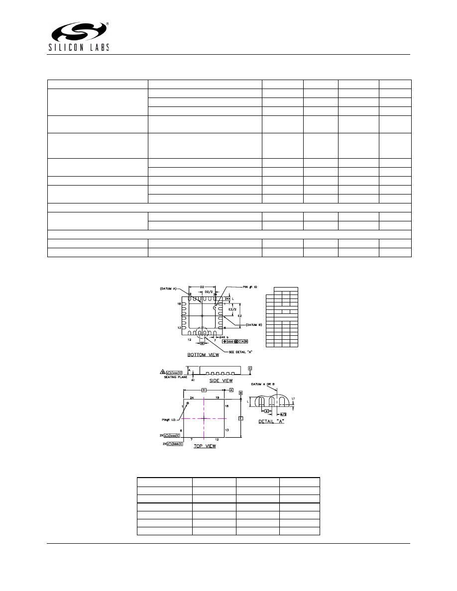
Package Information: 24-Pin QFN
MM
Min Typ Max
A
A1
b
D
D2
e
E
E2
L
L1
aaa
bbb
ccc
ddd
0.70 0.75 0.80
0.00 0.02 0.05
0.18 0.25 0.30
4.00 BSC
2.50 2.60 2.70
0.50 BSC
4.00 BSC
2.50 2.60 2.70
0.35 0.40 0.45
—
— 0.15
—
— 0.10
—
— 0.10
—
— 0.05
—
— 0.10
C8051F9xx Product Family
Device Part #
Package
Flash Size RAM Size
C8051F930-GQ
32-pin LQFP
64 kB
4 kB
C8051F930-GM
32-pin QFN
64 kB
4 kB
C8051F931-GM
24-pin QFN
64 kB
4 kB
C8051F920-GQ
32-pin LQFP
32 kB
4 kB
C8051F920-GM
32-pin QFN
32 kB
4 kB
C8051F921-GM
24-pin QFN
32 kB
4 kB
Wyszukiwarka
Podobne podstrony:
C8051F930 short
scripps short
pn2refresher short
L 5590 Short Sleeved Dress With Zipper Closure
MaturaSolutionsAdvanced Unit 10 short test 1 and 2
Koncepcja bezpieczeństwa USA SHORT VERSION, Dokumenty(2)
SHORT TEST IV
SHORT TEST V(1)
SHORT TEST I PODRÓŻOWANIE I TURYSTYKA (part I), ZAIMKI I PRZYMIOTNIKI DZIERŻAWCZE
SHORT TEST XIII
M 5532 Short dress
więcej podobnych podstron