Micrel’s Guide to
Designing With
Low-Dropout
Voltage
Regulators
Bob Wolbert
Applications Engineering Manager
Micrel Semiconductor
1849 Fortune Drive
San Jose, CA 95131
Phone:
+ 1 (408) 944-0800
Fax:
+ 1 (408) 944-0970
Revised Edition, December 1998
Micrel Semiconductor
Designing With LDO Regulators
Designing With LDO Regulators
2
Micrel, The High Performance Analog Power IC Company
Micrel Semiconductor designs, develops, manu-
factures, and markets high performance analog power
integrated circuits on a worldwide basis. These cir-
cuits are used in a wide variety of electronic prod-
ucts, including those in cellular communications, por-
table and desktop computers, and in industrial elec-
tronics.
Micrel History
Since its founding in 1978 as an independent
test facility of integrated circuits, Micrel has maintained
a reputation for excellence, quality and customer re-
sponsiveness that is second to none.
In 1981 Micrel acquired its first independent
semiconductor processing facility. Initially focusing
on custom and specialty fabrication for other IC manu-
facturers, Micrel eventually expanded to develop its
own line of semicustom and standard product Intelli-
gent Power integrated circuits. In 1993, with the con-
tinued success of these ventures, Micrel acquired a
new 57,000 sq. ft. facility and in 1995 expanded the
campus into a 120,000 sq. ft. facility. The new Class
10 facility has allowed Micrel to extend its process
and foundry capabilities with a full complement of
CMOS/DMOS/Bipolar/NMOS/PMOS processes. In-
corporating metal gate, silicon gate, dual metal, dual
poly and feature sizes down to 1.5 micron, Micrel is
able to offer its customers unique design and fabrica-
tion tools.
Micrel Today and Beyond
Building on its strength as an innovator in pro-
cess and test technology, Micrel has expanded and
diversified its business by becoming a recognized
leader in the high performance analog power control
and management markets.
The company’s initial public offering in Decem-
ber of 1994 and recent ISO9001 compliance are just
two more steps in Micrel’s long range strategy to be-
come the preeminent supplier of high performance
analog power management and control ICs. By stay-
ing close to the customer and the markets they serve,
Micrel will continue to remain focused on cost effec-
tive standard product solutions for an ever changing
world.
The niche Micrel has carved for itself involves:
• High Performance.....precision voltages, high tech-
nology (Super
β
eta PNP™ process, patented circuit
techniques, etc.) combined with the new safety
features of overcurrent, overvoltage, and overtem-
perature protection
• Analog.....we control continuously varying outputs of
voltage or current as opposed to digital ones and
zeros (although we often throw in “mixed signal” i.e.
analog with digital controls to bring out the best of
both worlds)
• Power ICs.....our products involve high voltage, high
current, or both
We use this expertise to address the following
growing market segments:
1. Power supplies
2. Battery powered computer, cellular phone,
and handheld instruments
3. Industrial & display systems
4. Desktop computers
5. Aftermarket automotive
6. Avionics
7. Plus many others
Copyright © 1998 Micrel, Inc.
All rights reserved. No part of this publication may be reproduced or used in any form or by any means
without written permission of Micrel, Incorporated.
Some products in this book are protected by one or more of the following patents: 4,914,546; 4,951,101;
4,979,001; 5,034,346; 5,045,966; 5,047,820; 5,254,486; and 5,355,008. Additional patents are pending.

3
Designing With LDO Regulators
Micrel Semiconductor
Designing With LDO Regulators
Contents
Low-Dropout␣ Linear␣ Regulators .................................................. 8
What is a Linear Regulator? ............................................................................... 8
Why Use Regulators? ........................................................................................... 8
Basic Design Issues .............................................................................................. 9
What is a “Low-Dropout” Linear␣ Regulator?................................................ 10
Linear Regulators vs. Switching␣ Regulators ................................................. 11
Who Prefers Linear Low Dropout Regulators? .................................................. 11
Section 2. Low-Dropout Regulator
Design Charts ................................................................................ 12
Regulator Selection Charts ............................................................................... 12
Regulator Selection Table ................................................................................. 14
Maximum Power Dissipation by Package Type ........................................... 16
Typical Thermal Characteristics ..................................................................... 17
Output Current vs. Junction Temperature and Voltage Differential ....... 18
Junction Temperature Rise vs. Available Output Current
Section 3. Using LDO Linear Regulators ..................................... 24
General Layout and Construction␣ Considerations ...................................... 24
Bypass Capacitors ................................................................................................... 24
Output Capacitor ..................................................................................................... 24
Circuit Board Layout ............................................................................................... 25
Adjustable Regulator Accuracy Analysis ............................................................ 27
Improving Regulator Accuracy ............................................................................. 28
Regulator & Reference Circuit Performance ....................................................... 29
Design Issues and General␣ Applications ...................................................... 31
Reference Generates a “Virtual VOUT” ............................................................... 31
Op-Amp Drives Ground Reference ...................................................................... 32
Click Any Item to
Jump to Page

Micrel Semiconductor
Designing With LDO Regulators
Designing With LDO Regulators
4
The Simplest Approach .......................................................................................... 34
Improving the Simple Approach........................................................................... 34
Eliminating Initial Start-Up Pedestal .................................................................... 35
Dropout Requirements ............................................................................................ 38
5V to 3.xV Conversion Circuits.............................................................................. 39
Method 1: Use a Monolithic LDO ......................................................................... 39
Method 2: The MIC5156 “Super LDO” ................................................................ 39
Method 3: The MIC5158 “Super LDO” ................................................................ 40
Method 4: Current Boost a MIC2951 .................................................................... 40
Adjust Resistor Values ............................................................................................ 40
3.3V to 2.xV Conversion .......................................................................................... 41
Improving Transient Response .............................................................................. 41
Accuracy Requirements .......................................................................................... 42
Multiple Output Voltages ...................................................................................... 43
Multiple Supply Sequencing .................................................................................. 44
Thermal Design ........................................................................................................ 44
Small Package Needed ........................................................................................... 45
Self Contained Power ............................................................................................. 45
Low Current (And Low Voltage) .......................................................................... 45
Low Output Noise Requirement ........................................................................... 45
Dropout and Battery Life ....................................................................................... 46
Ground Current and Battery Life .......................................................................... 46
Calculating Maximum Allowable Thermal␣ Resistance ..................................... 49
Why A Maximum Junction Temperature? ............................................................ 49
Heat Sink Charts for High Current Regulators................................................... 50
Thermal Examples ................................................................................................... 51
Heat Sink Selection ................................................................................................. 52
Reading Heat Sink Graphs ..................................................................................... 52
Power Sharing Resistor .......................................................................................... 53

5
Designing With LDO Regulators
Micrel Semiconductor
Designing With LDO Regulators
Determining Heat Sink Dimensions ..................................................................... 56
SO-8 Calculations: ................................................................................................... 57
Comments................................................................................................................. 58
Linear Regulator Troubleshooting Guide ..................................................... 59
Section 4. Linear Regulator Solutions .......................................... 60
eta PNP™ Regulators........................................................................... 60
Super beta PNP Circuitry ....................................................................................... 61
Dropout Voltage ....................................................................................................... 61
Ground Current ........................................................................................................ 62
Fully Protected ......................................................................................................... 62
Current Limiting ...................................................................................................... 62
Overtemperature Shutdown .................................................................................. 62
Reversed Input Polarity .......................................................................................... 62
Overvoltage Shutdown .......................................................................................... 63
Variety of Packages ................................................................................................. 63
Why Choose Five Terminal Regulators? .............................................................. 63
Compatible Pinouts ................................................................................................ 63
Stability Issues ........................................................................................................ 64
Paralleling Bipolar Regulators ............................................................................. 64
Micrel’s Unique “Super LDO™”..................................................................... 66
Micrel’s Super LDO Family ................................................................................... 66
The MIC5156 ............................................................................................................. 66
The MIC5157 and MIC5158 .................................................................................... 66
3.3V, 10A Regulator Application ........................................................................... 66
Comparison With Monolithics.............................................................................. 67
Super High-Current Regulator .............................................................................. 67
Selecting the Current Limit Threshold ................................................................. 69
Sense Resistor Power Dissipation ......................................................................... 69
Kelvin Sensing ......................................................................................................... 69
Resistor Design Method ......................................................................................... 70
Design Example ....................................................................................................... 70
Calculate Sheet Resistance ..................................................................................... 71
Calculate Minimum Trace Width .......................................................................... 71
Calculate Required Trace Length .......................................................................... 71
Resistor Layout ........................................................................................................ 71
Thermal Considerations ......................................................................................... 71

Micrel Semiconductor
Designing With LDO Regulators
Designing With LDO Regulators
6
Section 5. Omitted ............................................................................ 74
Section 6. Package Information...................................................... 75
Packaging for Automatic Handling ................................................................ 76
Package Orientation ........................................................................................... 77
Linear Regulator Packages ............................................................................... 78
8-Pin Plastic DIP (N) ............................................................................................... 78
14-Pin Plastic DIP (N) ............................................................................................. 78
8-Pin SOIC (M) ......................................................................................................... 79
14-Pin SOIC (M) ....................................................................................................... 79
TO-92 (Z) ................................................................................................................... 80
SOT-223 (S) ............................................................................................................... 80
SOT-143 (M4) ............................................................................................................ 81
SOT-23 (M3) .............................................................................................................. 81
SOT-23-5 (M5) .......................................................................................................... 82
MSOP-8 [MM8™] (MM) ......................................................................................... 82
3-Lead TO-220 (T) .................................................................................................... 83
5-Lead TO-220 (T) .................................................................................................... 83
5-Lead TO-220 Vertical Lead Bend Option (-LB03) ............................................ 84
5-Lead TO-220 Horizontal Lead Bend Option (-LB02) ...................................... 84
3-Lead TO-263 (U) ................................................................................................... 85
5-Lead TO-263 (U) ................................................................................................... 85
Typical 3-Lead TO-263 PCB Layout ...................................................................... 86
Typical 5-Lead TO-263 PCB Layout ...................................................................... 86
3-Lead TO-247 (WT) ................................................................................................ 87
5-Lead TO-247 (WT) ................................................................................................ 88
Section 7. Appendices ...................................................................... 89
Appendix A. Table of Standard 1% Resistor Values.................................... 90
Appendix B. Table of Standard
10% Resistor Values .............. 91
Appendix C. LDO SINK for the HP 48 Calculator....................................... 92
Section 8. Low-Dropout Voltage Regulator Glossary ................ 95
Section 9. References ........................................................................ 97
Section 10. Index ............................................................................... 98
Section 11. Worldwide
Representatives and Distributors ............................................ 100
Micrel Sales Offices ......................................................................................... 100
U.S. Sales Representatives .............................................................................. 101
U.S. Distributors ............................................................................................... 103
International Sales Representatives and Distributors .............................. 107

7
Designing With LDO Regulators
Micrel Semiconductor
Designing With LDO Regulators
Contributors:
Jerry Kmetz
Mike Mottola
Jim Cecil
Brian Huffman
Marvin Vander Kooi
Claude Smithson
Micrel Semiconductor
1849 Fortune Drive
San Jose, CA 95131
Phone:
+ 1 (408) 944-0800
Fax:
+ 1 (408) 944-0970
http://www.micrel.com
Micrel Semiconductor
Designing With LDO Regulators
Section 1: Introduction
8
Designing With LDO Regulators
Section 1. Introduction:
Low-Dropout␣ Linear␣ Regulators
op-amp increases drive to the pass element, which
increases output voltage. Conversely, if the output
rises above the desired set point, the op amp reduces
drive. These corrections are performed continuously
with the reaction time limited only by the speed of the
op amp and output transistor loop.
Real linear regulators have a number of other
features, including protection from short circuited
loads and overtemperature shutdown. Advanced
regulators offer extra features such as overvoltage
shutdown, reversed-insertion and reversed polarity
protection, and digital error indicators that signal when
the output is not correct.
Why Use Regulators?
Their most basic function, voltage regulation,
provides clean, constant, accurate voltage to a cir-
cuit. Voltage regulators are a fundamental block in
the power supplies of most all electronic equipment.
Key regulator benefits and applications include:
•
Accurate supply voltage
•
Active noise filtering
•
Protection from overcurrent faults
•
Inter-stage isolation (decoupling)
•
Generation of multiple output voltages from a
single source
•
Useful in constant current sources
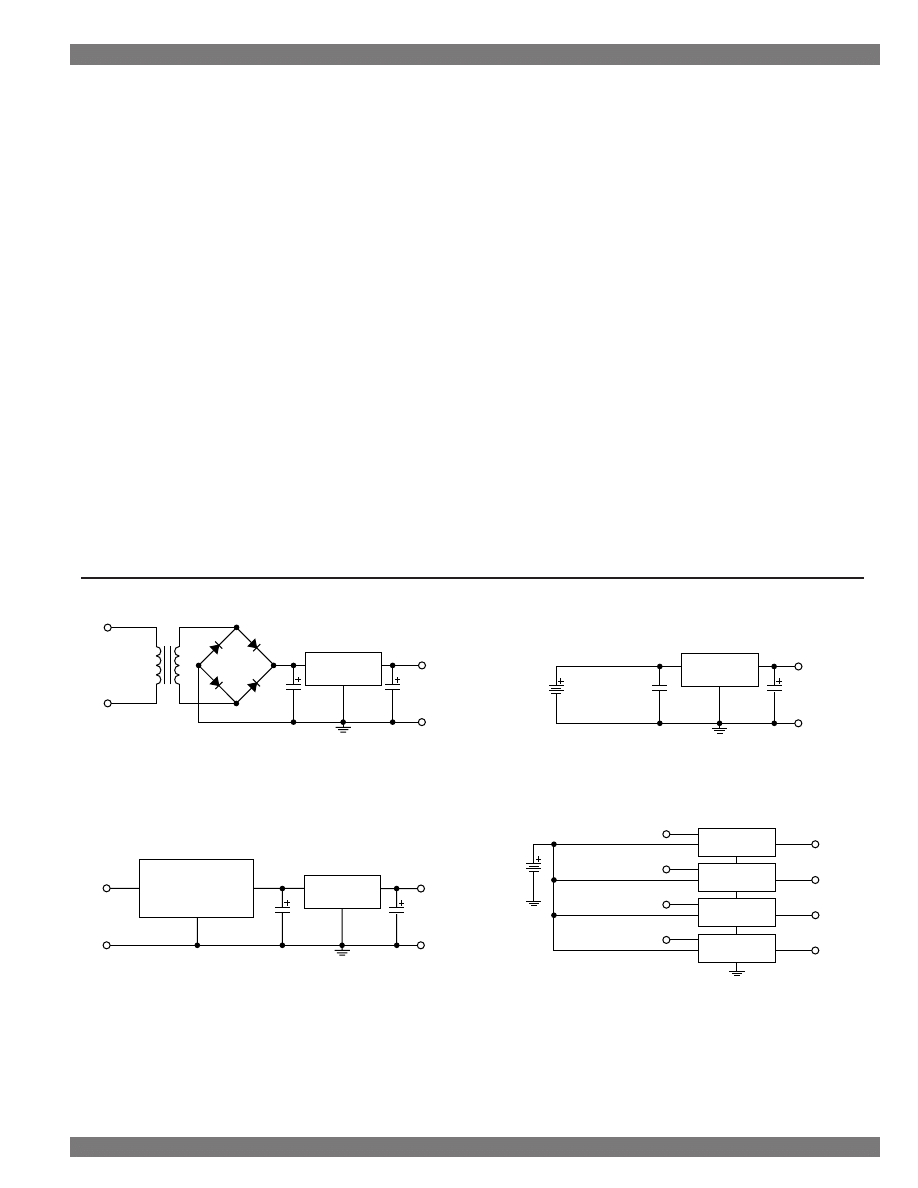
Figure 1-2 shows several typical applications for
linear voltage regulators. A traditional AC to DC power
supply appears in Figure 1-2(A). Here, the linear regu-
lator performs ripple rejection, eliminating AC hum,
and output voltage regulation. The power supply out-
put voltage will be clean and constant, independent
of AC line voltage variations. Figure 1-2(B) uses a
low-dropout linear regulator to provide a constant
output voltage from a battery, as the battery dis-
charges. Low dropout regulators are excellent for this
application since they allow more usable life from a
given battery. Figure 1-2(C) shows a linear regulator
configured as a “post regulator” for a switching power
What is a Linear Regulator?
IC linear voltage regulators have been around
for decades. These simple-to-use devices appear in
nearly every type of electronic equipment, where they
produce a clean, accurate output voltage used by
sensitive components.
Historically, linear regulators with PNP outputs
have been expensive and limited to low current ap-
plications. However, Micrel Semiconductor’s unique
“Super
β
eta PNP™” line of low dropout regulators
provides up to 7.5 amperes of current with dropout
voltages less than 0.6V, guaranteed. A lower cost
product line outputs the same currents with only 1V
of dropout. These low dropout voltages guarantee the
microprocessor gets a clean, well regulated supply
that quickly reacts to processor-induced load changes
as well as input supply variations.
The low dropout linear voltage regulator is a
easy-to-use, low cost, yet high performance means
of powering your systems.
Input
Ground
Output
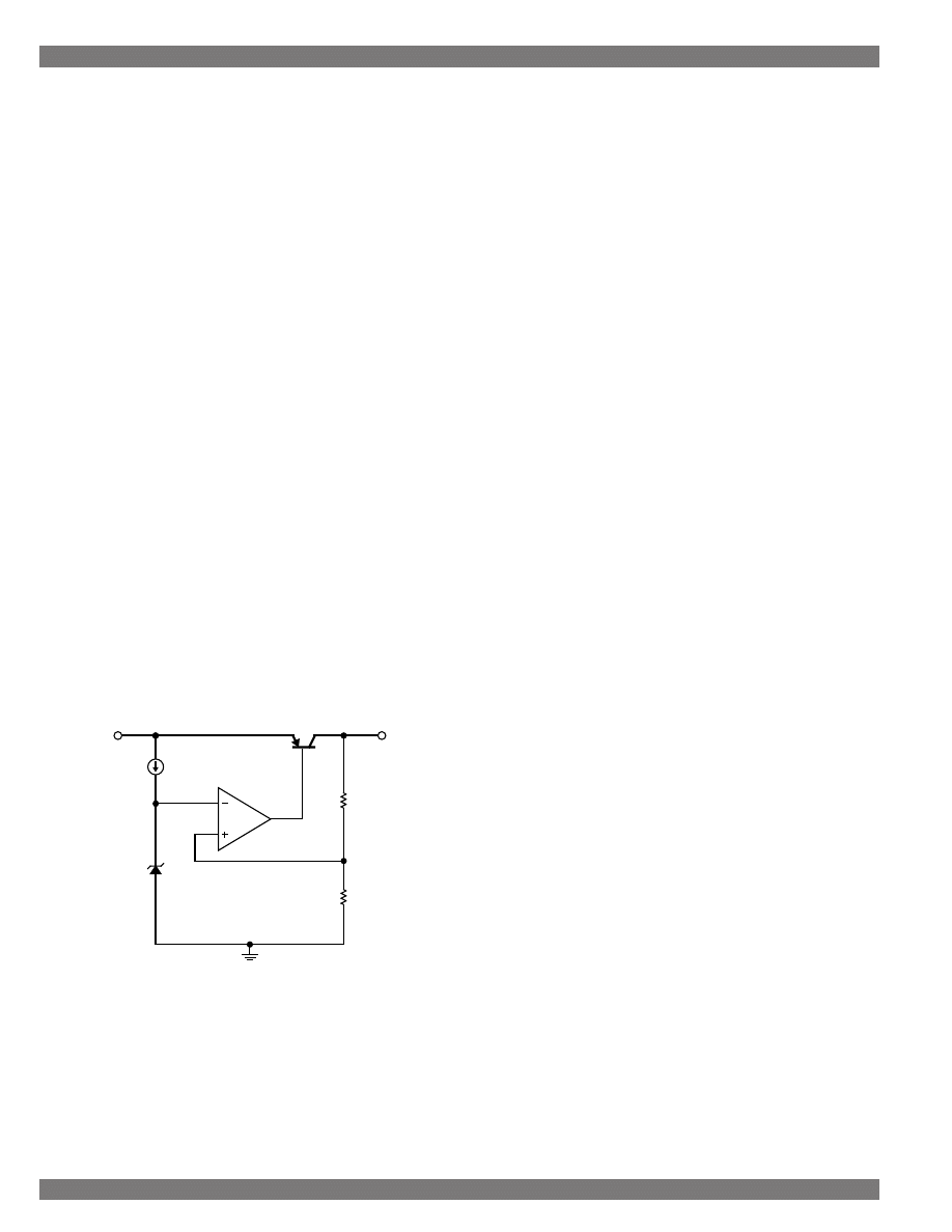
Figure 1-1. A basic linear regulator schematic.
A typical linear regulator diagram is shown in
Figure 1-1. A pass transistor is controlled by an op-
erational amplifier which compares the output volt-
age to a reference. As the output voltage drops, the
Designing With LDO Regulators
9
Section 1: Introduction
Micrel Semiconductor
Designing With LDO Regulators
supply. Switching supplies are known for excellent ef-
ficiency, but their output is noisy; ripple degrades
regulation and performance, especially when power-
ing analog circuits. The linear regulator following the
switching regulator provides active filtering and greatly
improves the output accuracy of the composite sup-
ply. As Figure 1-2(D) demonstrates, some linear regu-
lators serve a double duty as both regulator and power
ON/OFF control. In some applications, especially ra-
dio systems, different system blocks are often pow-
ered from different regulators—even if they use the
same supply voltage—because of the isolation (de-
coupling) the high gain regulator provides.
Basic Design Issues
Let’s review the most important parameters of
voltage regulators:
•
Output voltage is an important parameter, as this
is the reason most designers purchase a regula-
tor. Linear regulators are available in both fixed
output voltage and adjustable configurations.
Fixed voltage regulators offer enhanced ease-of-
use, with their output voltages accurately trimmed
at the factory—but only if your application uses
an available voltage. Adjustables allow using a
voltage custom-tailored for your circuit.
•
Maximum output current is the parameter gener-
ally used to group regulators. Larger maximum
output currents require larger, more expensive
regulators.
•
Dropout voltage is the next major parameter. This
is the minimum additional voltage on the input that
still produces a regulated output. For example, a
Micrel 5.0V Super
β
eta PNP regulator will pro-
vide regulated output with an input voltage of 5.3V
or above. The 300mV term is the dropout volt-
age. In the linear regulator world, the lower the
dropout voltage, the better.
•
Ground current is the supply current used by the
regulator that does not pass into the load. An ideal
regulator will minimize its ground current. This
parameter is sometimes called quiescent current,
but this usage is incorrect for PNP-pass element
regulators.
Figure 1-2. Typical Linear Regulator Applications
(D) “Sleep-mode” and Inter Stage Isolation or De-
coupling
(C) Post-Regulator for Switching Supplies
AC or DC
Input
Clean
DC Output
Low-Dropout
Linear Regulator
Switching Regulator
(High efficiency,
but noisy output)
Output 1
Low-Dropout
Linear Regulator
Battery
Low-Dropout
Linear Regulator
Low-Dropout
Linear Regulator
Low-Dropout
Linear Regulator
Output 2
Output 3
Output 4
Enable 1
Enable 2
Enable 3
Enable 4
(A) Standard Power Supplies
(B) Battery Powered Applications
AC Input
DC Output
Low-Dropout
Linear Regulator
DC Output
Low-Dropout
Linear Regulator
Battery
Micrel Semiconductor
Designing With LDO Regulators
Section 1: Introduction
10
Designing With LDO Regulators
•
Efficiency is the amount of usable (output) power
achieved from a given input power. With linear
regulators, the efficiency is approximately the
output voltage divided by the input voltage.
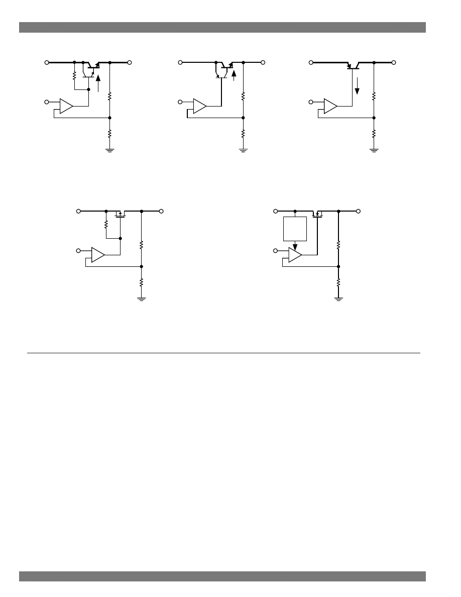
What is a “Low-Dropout”
Linear␣ Regulator?
A low dropout regulator is a class of linear regu-
lator that is designed to minimize the saturation of
the output pass transistor and its drive requirements.
A low-dropout linear regulator will operate with input
voltages only slightly higher than the desired output
voltage. For example, “classic” linear regulators, such
as the 7805 or LM317 need about 2.5 to 3V higher
input voltage for a given output voltage. For a 5V out-
put, these older devices need a 8V input. By com-
parison, Micrel’s Super beta PNP low dropout regu-
Input
Output
VREF
VDO (MIN) = VBE (Q1) + VBE (Q2)
+ VSAT current source (if used)
+
–
Drive
Current
Q1
Q2
current source
or resistor
Input
Output
VREF
VDO (MIN) = VSAT (Q2) +VBE (Q1)
+
–
Drive
Current
Q1
Q2
Input
Output
VREF
VDO (MIN) = VSAT
+
–
Drive
Current
Input
Output
VREF
VDO (MIN) = RDS (ON)(Q1)
×
IOUT
+
–
Q1
charge
pump
voltage
multiplier
Input
Output
VREF
VDO (MIN) = RDS (ON)(Q1)
×
IOUT
+
–
Q1
current source
or resistor
(D) P-Channel MOSFET-pass transistor regulator
(E) N-Channel MOSFET-pass transistor regulator
Figure 1-3. The Five Major Types of Linear Regulators
(A) Standard NPN-pass transistor
regulator
(C) Low-Dropout PNP-pass tran-
sistor regulator
(B) NPN-pass regulator with
reduced dropout
lators require only 0.3V of headroom, and would pro-
vide regulated output with only 5.3V of input.
Figure 1-3 shows the five major types of linear
regulators:
A. “Classic” NPN-based regulators that require 2.5
to 3V of excess input voltage to function.
B. “Low Dropout NPN” regulators, with a NPN out-
put but a PNP base drive circuit. These devices
reduce the dropout requirement to 1.2 to 1.5V.
C. True low dropout PNP-based regulators that need
0.3V to 0.6V extra for operation.
D. P-channel CMOS output regulators. These de-
vices have very low dropout voltages at low cur-
rents but require large die area (hence higher
costly than bipolar versions) and have high inter-
nal drive current requirements when working with
noisy inputs or widely varying output currents.
Designing With LDO Regulators
11
Section 1: Introduction
Micrel Semiconductor
Designing With LDO Regulators
E. Regulator controllers. These are integrated cir-
cuits that provide the reference and control func-
tions of a linear regulator, but do not have the
pass element on board. They provide the advan-
tage of optimizing die area and cost for higher
current applications but suffer the disadvantage
of being a multiple package solution.
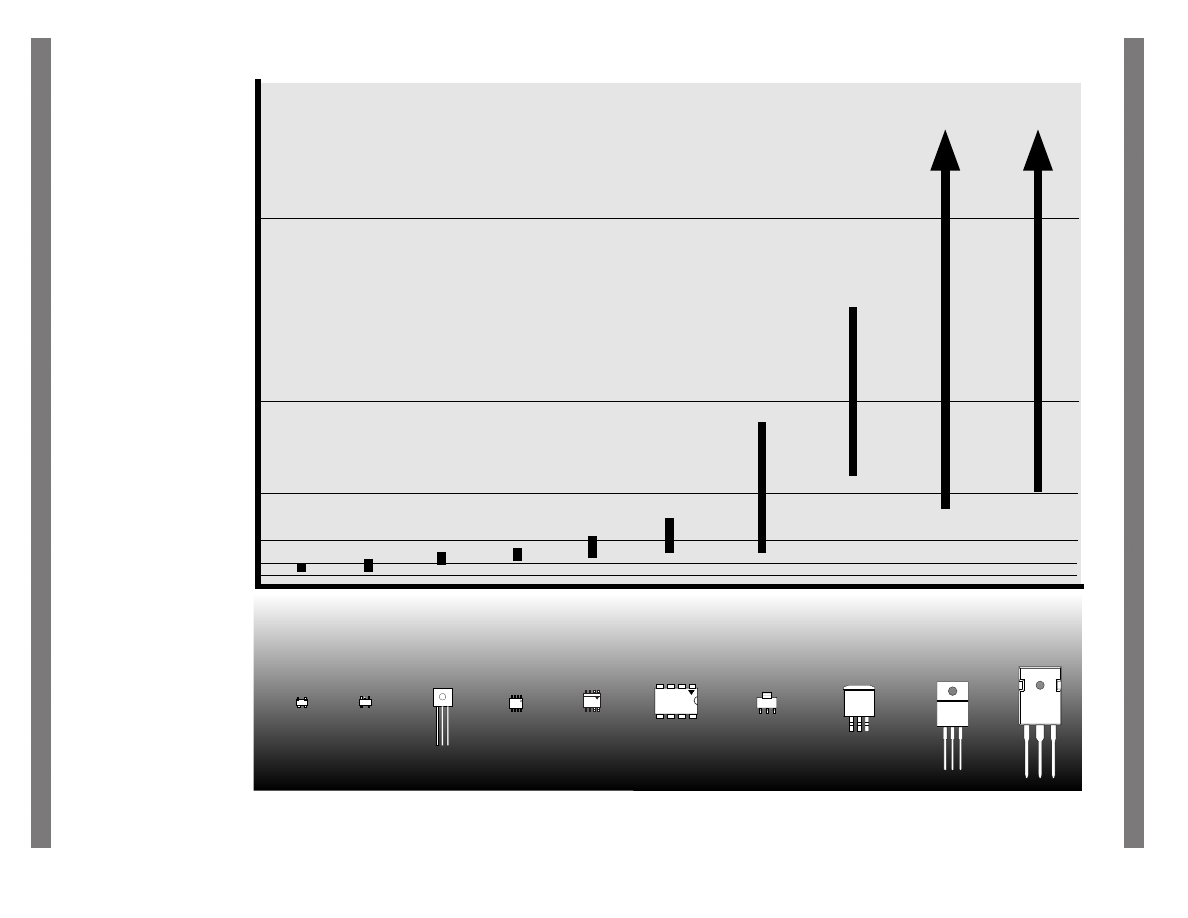
If we graph the efficiency of the different classes
of linear regulators we see very significant differences
at low input and output voltages (see Figure 1-4). At
higher voltages, however, these differences dimin-
ish. A 3.3V high current linear regulator controller such
as the Micrel MIC5156 can approach 100% efficiency
as the input voltage approaches dropout. But an
LM317 set to 3.3V at 1A will have a miserable effi-
ciency of only about 50% at its dropout threshold.
Linear Regulators vs.
Switching␣ Regulators
Linear regulators are less energy efficient than
switching regulators. Why do we continue using
them? Depending upon the application, linear regu-
lators have several redeeming features:
•
lower output noise is important for radios and other
communications equipment
•
faster response to input and output transients
•
easier to use because they require only filter ca-
pacitors for operation
•
generally smaller in size (no magnetics required)
•
less expensive (simpler internal circuitry and no
magnetics required)
Figure 1-4. Linear Regulator Efficiency at Dropout
Furthermore, in applications using low input-to-
output voltage differentials, the efficiency is not all
that bad! For example, in a 5V to 3.3V microproces-
sor application, linear regulator efficiency approaches
66%. And applications with low current subcircuits
may not care that regulator efficiency is less than
optimum as the power lost may be negligible overall.
Who Prefers Linear Low Dropout
Regulators?
We see that price sensitive applications prefer
linear regulators over their sampled-time counterparts.
The design decision is especially clear cut for mak-
ers of:
•
communications equipment
•
small devices
•
battery operated systems
•
low current devices
•
high performance microprocessors with sleep
mode (fast transient recovery required)
As you proceed through this book, you will find
numerous other applications where the linear regu-
lator is the best power supply solution.
100
50
80
60
8
1
OUTPUT CURRENT (A)
LM340
LM317 LM350
LM396
LT1083
LT1086
LT1085
LT1084
MIC5156/7/8
MIC5203
MIC5200
MIC29750
MIC29300 MIC29500
MIC29150
MIC2920
MIC5201
100
0.4
0.2
0.1
4
6
78L05
2
EFFICIENCY AT DROPOUT (%)
Micrel Semiconductor
Designing With LDO Regulators
Section 2: Design Charts
12
Designing With LDO Regulators
Section 2. Low-Dropout Regulator
Design Charts
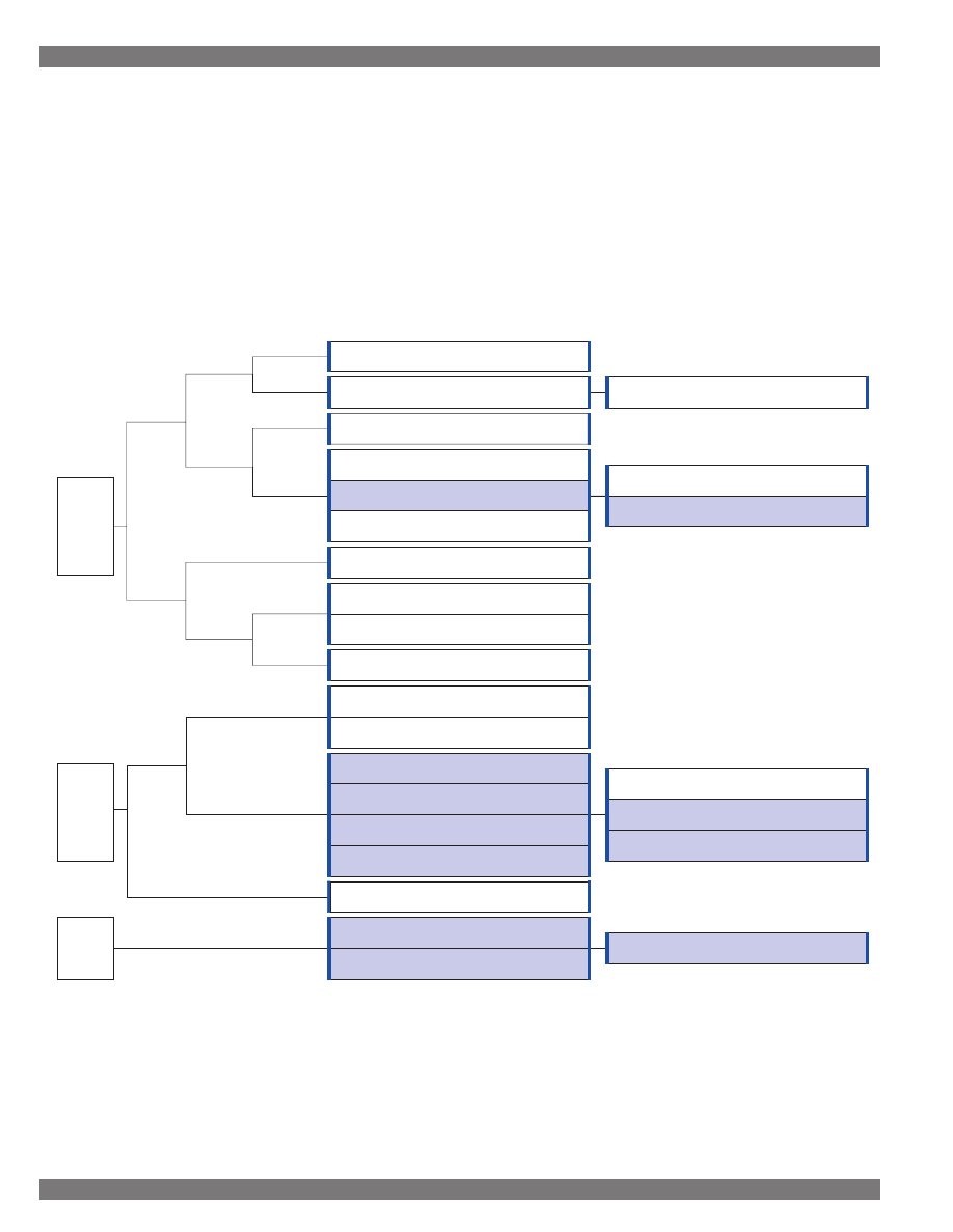
Regulator Selection Charts
Output
Current
Accuracy
Low
Noise
Single
or Dual
0 –180mA
200mA –
500mA
Without Error Flag
With Error Flag
MIC5210
Dual 150mA LDO w/ Noise Bypass
MSOP-8
3.0, 3.3, 3.6, 4.0, 5.0V
MIC5205
150mA LDOw/ Noise Bypass
SOT23-5
2.8, 3.0, 3.3, 3.6, 3.8, 4.0, 5.0V, Adj
MIC5202
Dual 100mA LDO
SO-8
3.0, 3.3, 4.5, 4.85, 5.0V
LP2950
100mA LDO Second Source to '2950
TO-92
5.0V
MIC2950
150mA LDO Upgrade to '2950
TO-92
5.0V
MIC5200 100mA
LDO
SO-8, SOT-223, MSOP-8
3.0, 3.3, 4.85, 5.0V
MIC5207 180mA
LDO
SOT23-5, TO-92
1.8, 2.5, 3.0, 3.3, 3.6, 3.8, 5.0V, Adj
MIC5211 Dual
50mA
µ
Cap LDO
SOT23-6
2.5, 3.0, 3.3, 3.6, 5.0, Mixed 3.3/5.0V
MIC5208 Dual
50mA
µ
Cap LDO
MSOP-8
3.0, 3.3, 3.6, 4.0, 5.0V
MIC5203 80mA
µ
Cap LDO
SOT-143, SOT23-5
2.8, 3.0, 3.3, 3.6, 3.8, 4.0, 5.0V
MIC5206
150mA LDOs w Noise Bypass
SOT23-5, MSOP-8
2.5, 3.0, 3.3, 3.6, 4.0, 5.0V, Adj
LP2951
100mA LDO Second Source to '2951
SO-8, PDIP-8
4.85, 5.0V, Adj
MIC2951
150mA LDO Upgrade to '2951
SO-8, PDIP-8, MSOP-8
3.3, 4.85, 5.0V, Adj
MIC5219
500mA Peak LDO
SOT23-5, MSOP-8
3.0, 3.3, 3.6, 5.0V, Adj
MIC5209 500mA
LDO
SOT223, SO-8, TO263-5
1.8, 2.5, 3.0, 3.3, 5.0V, Adj
MIC5201
200mA LDO
SOT223, SO-8
3.0, 3.3, 4.85, 5.0V, Adj
MIC2954
250mA LDO
TO220, SOT223, SO-8, TO92
5.0V, Adj
MIC2920 400mA
LDO
TO220, SOT223
3.3, 4.85, 5.0V
MIC29202 400mA
LDO
TO220, TO263
Adj
MIC5237 500mA
LDO
TO220, TO263
2.5, 3.3, 5.0V
MIC29371
750mA LDO
TO220, TO263
3.3, 5.0V
MIC2937A 750mA
LDO
TO220, TO263
3.3, 5.0, 12.0V
MIC29372
750mA LDO
TO220, TO263
Adj
750mA
MIC5216
500mA Peak LDO
SOT23-5, MSOP-8
3.0, 3.3, 3.6, 5.0V
MIC29201
400mA LDO
TO220, TO263, SO-8
3.3, 4.85, 5.0V
MIC29204
400mA LDO
SO-8
Adj
Yes
No
Yes
No
±
1.0%
±
3.0%
Dual
Single
Dual
Single
Dual
Single
±
1.0%
±
3.0%
Yes
No
±
1.0%
Single
Single
Single
Single
No
No
Figure 2-1a. 0 to 750mA LDO Regulator Selection Guide
Shaded boxes denote automotive load dump protected devices
Designing With LDO Regulators
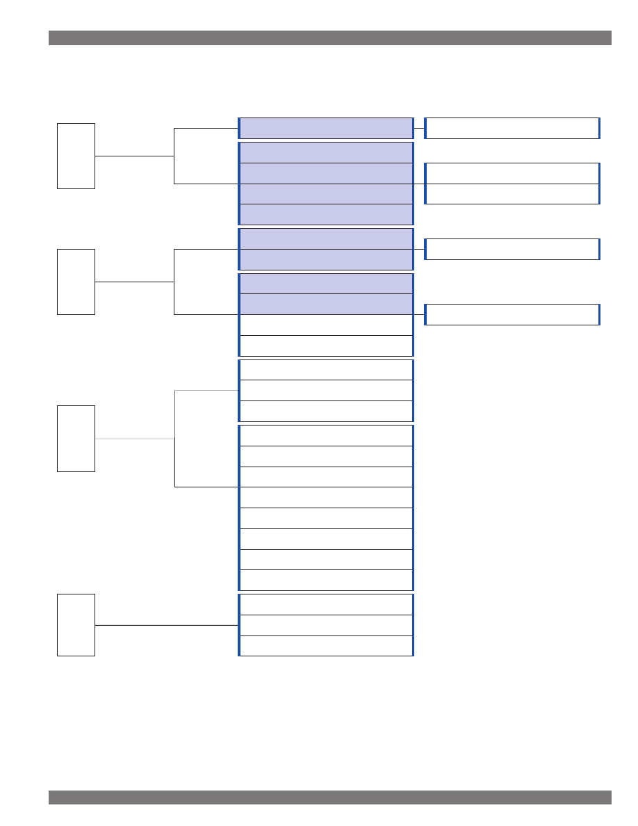
13
Section 2: Design Charts
Micrel Semiconductor
Designing With LDO Regulators
Output
Current
Accuracy
Error Flag
1A –
1.5A
3.0A
Low-Dropout Devices
Ultra-Low-Dropout Devices
MIC29151
1.5A LDO
TO220, TO263
3.3, 5.0, 12V
MIC2940A 1.25A
LDO
TO220, TO263
3.3, 5.0, 12V
MIC2941A 1.25A
LDO
TO220, TO263
Adj
MIC29150
1.5A LDO
TO220, TO263
3.3, 5.0, 12.0V
MIC29152
1.5A LDO
TO220, TO263
Adj
MIC29301
3.0A LDO
TO220, TO263
3.3, 5.0, 12V
MIC29303
3.0A LDO
TO220, TO263
Adj
MIC39151
1.5A LDO
TO263
1.8, 2.5V
MIC39150
1.5A LDO
TO220, TO263
1.8, 2.5V
MIC29300 3.0A
LDO
TO220, TO263
3.3, 5.0, 12.0V
MIC29302 3.0A
LDO
TO220, TO263
Adj
MIC29310
3.0A Low Cost LDO
TO220, TO263
3.3, 5.0V
MIC29312
3.0A Low Cost LDO
TO220, TO263
Adj
MIC29501 5.0A
LDO
TO220, TO263
3.3, 5.0V
MIC29503 5.0A
LDO
TO220, TO263
Adj
MIC29751 7.5A
LDO
TO247
3.3, 5.0V
MIC39300
3.0A LDO
TO220, TO263
1.8, 2.5V
MIC29500 5.0A
LDO
TO220, TO263
3.3, 5.0V
MIC29502 5.0A
LDO
TO220, TO263
Adj
MIC29510
5.0A Low Cost LDO
TO220
3.3, 5.0V
MIC29512
5.0A Low Cost LDO
TO220
Adj
MIC29750 7.5A
LDO
TO247
3.3, 5.0V
MIC29752
7.5A Low Cost LDO
TO247
Adj
MIC29710 7.5A
LDO
TO220
3.3, 5.0V
MIC29712
7.5A Low Cost LDO
TO220
Adj
MIC39301
3.0A LDO
TO263, TO220
1.8, 2.5V
MIC39100
1.0A LDO
SOT223
1.8, 2.5, 3.3V
MIC5156 LDO
Controller
SO-8, PDIP-8
3.3, 5.0V, Adj
MIC5157
LDO Controller (w/Charge Pump)
SO-14, PDIP-14
3.3, 5.0, 12V
MIC5158
LDO Controller (w/Charge Pump)
SO-14, PDIP-14
5.0V, Adj
±
1.0%
±
1.0%
5.0A –-
7.5A
±
1.0%
Yes
No
Yes
No
Yes
No
>7.5A
±
1.0%
Yes
Figure 2-1b. 1A to >7.5A LDO Regulator Selection Guide
Shaded boxes denote automotive load dump protected devices
Micrel Semiconductor
Designing
With LDO Regulator
s
Section 2:
Design Char
ts
14
Designing
With LDO Regulator
s
Output
Standard Output Voltage
Adj.
Dropout
Current Error
Enable/
Thermal
Rev. Input
Load
Device
Current
1.8 2.5 2.8 3.0 3.3 3.6 3.8 4.0 4.75 4.85 5.0 12
(max.)
Accuracy
(I
MAX
, 25
°
C) Limit
Flag Shutdown Shutdown
Protection
Dump
Packages
MIC5208
50mA
×
2
•
•
•
•
•
3%
250mV
•
•
•
•
MSOP-8
MIC5211
50mA
×
2
•
•
•
•
•
3%
250mV
•
•
•
•
SOT-23-6
MIC5203
80mA
•
•
•
•
•
•
•
•
3%
300mV
•
•
•
•
SOT-143, SOT-23-5
MIC5200
100mA
•
•
•
•
1%
230mV
•
•
•
•
SOP-8, SOT-223, MSOP-8
MIC5202
100mA
×
2
•
•
•
•
1%
225mV
•
•
•
•
SOP-8
LP2950
100mA
•
1
⁄
2
%,1% 380mV
•
•
TO-92
LP2951
100mA
•
•
29V
1
⁄
2
%,1% 380mV
•
•
•
•
DIP-8, SOP-8
MIC2950
150mA
•
1
⁄
2
%,1% 300mV
•
•
•
•
TO-92
MIC2951
150mA
•
•
•
29V
1
⁄
2
%,1% 300mV
•
•
•
•
•
•
DIP-8, SOP-8, MSOP-8
MIC5205
150mA
•
•
•
•
•
•
•
16V
1%
165mV
•
•
•
•
SOT-23-5
MIC5206
150mA
•
•
•
•
•
•
16V
1%
165mV
•
•
•
•
•
SOT-23-5, MSOP-8
MIC5210
150mA
×
2
•
•
•
•
•
1%
165mV
•
•
•
•
MSOP-8
MIC5207
180mV
•
•
•
•
•
•
•
•
16V
3%
165mA
•
•
•
•
SOT-23-5, TO-92
SP
MIC5201
200mA
•
•
•
16V
1%
270mV
•
•
•
•
SOP-8, SOT-223
MIC2954
250mA
•
29V
1
⁄
2
%
375mV
•
•
•
•
•
•
TO-92,TO-220,SOT-223
MIC2920A
400mA
•
•
•
•
1%
450mV
•
•
•
•
TO-220, SOT-223
MIC29201
400mA
•
•
•
SP
1%
450mV
•
•
•
•
•
•
TO-220-5, TO-263-5
MIC29202
400mA
26V
1%
450mV
•
•
•
•
•
TO-220-5, TO-263-5
MIC29204
400mA
•
26V
1%
450mV
•
•
•
•
•
•
SOP-8, DIP-8
MIC5216
500mA
(1)
•
•
•
•
12V
1%
300mV
•
•
•
•
•
SOT-23-5, MSOP-8
MIC5219
500mA
(1)
•
•
•
•
12V
1%
300mV
•
•
•
•
SOT-23-5, MSOP-8
MIC5209
500mA
•
•
•
•
•
•
16V
1%
300mV
•
•
•
•
SOP-8, SOT-223, TO-263-5
MIC5237
500mA
•
•
•
16V
3%
300mV
•
•
•
TO-220, TO-263
MIC2937A
750mA
•
•
•
1%
370mV
•
•
•
•
TO-220, TO-263
MIC29371
750mA
•
•
SP
1%
370mV
•
•
•
•
•
•
TO-220-5, TO-263-5
MIC29372
750mA
26V
1%
370mV
•
•
•
•
•
TO-220-5, TO-263-5
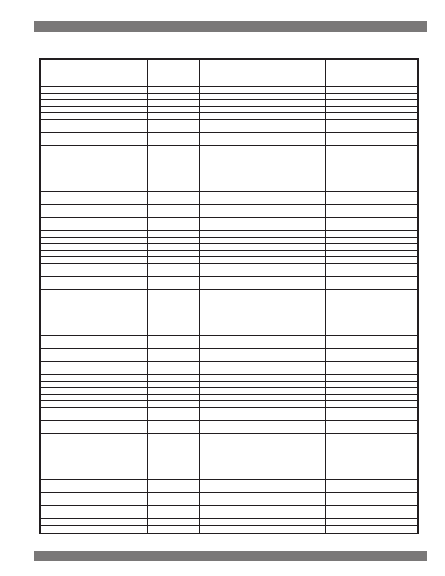
Regulator Selection Table
(Sorted by Output Current Rating)
Designing
With LDO Regulator
s
1
5
Section 2:
Design Char
ts
Micrel Semiconductor
Designing
With LDO Regulator
s
Output
Standard Output Voltage
Adj.
Dropout
Current Error
Enable/
Thermal
Rev. Input
Load
Device
Current 1.8 2.5 2.8 3.0 3.3 3.6 3.8 4.0 4.75 4.85 5.0 12
(max.)
Accuracy
(I
MAX
, 25
°
C) Limit
Flag Shutdown Shutdown
Protection
Dump
Packages
MIC2940A
1.25A
•
•
•
1%
400mV
•
•
•
•
TO-220, TO-263
MIC2941A
1.25A
26V
1%
400mV
•
•
•
•
•
TO-220-5, TO-263-5
MIC29150
1.5A
•
•
•
1%
350mV
•
•
•
•
TO-220, TO-263
MIC29151
1.5A
•
•
•
1%
350mV
•
•
•
•
•
•
TO-220-5, TO-263-5
MIC29152
1.5A
26V
1%
350mV
•
•
•
•
•
TO-220-5, TO-263-5
MIC29153
1.5A
26V
SP
1%
350mV
•
•
•
•
•
TO-220-5, TO-263-5
MIC39150
1.5A
•
1%
350mV
•
•
•
TO-220, TO-263
MIC39151
1.5A
•
1%
350mV
•
•
•
•
•
TO-220-5, TO-263-5
MIC29300
3A
•
•
•
1%
370mV
•
•
•
•
TO-220, TO-263
MIC29301
3A
•
•
•
1%
370mV
•
•
•
•
•
•
TO-220-5, TO-263-5
MIC29302
3A
26V
1%
370mV
•
•
•
•
•
TO-220-5, TO-263-5
MIC29303
3A
26V
1%
370mV
•
•
•
•
•
TO-220-5, TO-263-5
MIC29310
3A
•
•
2%
600mV
•
•
TO-220, TO-263
MIC29312
3A
16V
2%
600mV
•
•
•
TO-220-5, TO-263-5
MIC39300
3A
•
1%
400mV
•
•
•
TO-220, TO-263
MIC39301
3A
•
1%
400mV
•
•
•
•
•
TO-220-5, TO-263-5
MIC29500
5A
•
•
1%
370mV
•
•
•
•
TO-220
MIC29501
5A
•
•
1%
370mV
•
•
•
•
•
•
TO-220-5, TO-263-5
MIC29502
5A
26V
1%
370mV
•
•
•
•
•
TO-220-5, TO-263-5
MIC29503
5A
26V
1%
370mV
•
•
•
•
•
TO-220-5, TO-263-5
MIC29510
5A
•
•
2%
700mV
•
•
TO-220, TO-263
MIC29512
5A
16V
2%
700mV
•
•
•
TO-220-5
MIC29710
7.5A
•
•
2%
700mV
•
•
TO-220
MIC29712
7.5A
16V
2%
700mV
•
•
•
TO-220-5
MIC29750
7.5A
•
•
1%
425mV
•
•
•
•
TO-247
MIC29751
7.5A
•
•
1%
425mV
•
•
•
•
•
•
TO-247-5
MIC29752
7.5A
26V
1%
425mV
•
•
•
•
•
TO-247-5
MIC5156
(2)
•
•
36V
1%
(2)
•
•
•
•
SOP-8, DIP-8
MIC5157
(2)
(3)
(3)
(3)
1%
(2)
•
•
•
SOP-14, DIP-14
MIC5158
(2)
(4)
(4)
1%
(2)
•
•
•
SOP-14, DIP-14
SP
Special order. Contact factory.
1
Output current limited by package and layout.
2
Maximum output current and dropout voltage are determined by the choice of external MOSFET.
3
3.3V, 5V, or 12V selectable operation.
4
5V or Adjustable operation.
Micrel Semiconductor
Designing
With LDO Regulator
s
Section 2:
Design Char
ts
16
Designing
With LDO Regulator
s
The minimum point on each line of Figure 2-3 shows package power dissipation capability using “worst
case”
mounting techniques
. The maxim
um point sho
ws po
wer capability with a v
e
ry
good (not infinite
, though)
heat sink.
F
or e
xample
, through-hole
T
O-220 pac
kages can dissipate a bit less than 2W without a heat sink,
and o
v
er 30W with a good sink.
The char
t is appro
ximate
, and assumes an ambient temper
ature of 25
°
C.
Packages are
not
shown in their approximate relative size.
Maximum Power Dissipation by Package Type
> 30W
> 50W
5W
1W
0
2W
3W
4W
6W
7W
8W
9W
10W
SOT-143
SOT-23-5
SOT-223
Figure 2-3
Designing With LDO Regulators
17
Section 2: Design Charts
Micrel Semiconductor
Designing With LDO Regulators
Device
θ
JC
θ
CS
“Typical” heat
Equivalent Thermal
sink
θ
JA
Graph
(Figures 2-6, 2-7)
MIC5203BM4
—
—
250
A
MIC5200BM
—
—
160
B
MIC5200BS
15
—
50
E
MIC5202BM
—
—
160
B
LP2950BZ
—
—
160 – 180
B
LP2951BM
—
—
160
B
MIC2950BZ
—
—
160 – 180
D
MIC2951BM
—
—
160
D
MIC2951BN
—
—
105
MIC5205BM5
—
—
220
C
MIC5206BM5
—
—
220
C
MIC5206BMM
—
—
200
C
MIC5207BM5
—
—
220
C
MIC5201BM
—
—
160
D
MIC5201BS
15
—
50
E
MIC2954BM
—
—
160
MIC2954BS
15
—
50
MIC2954BT
3
1
15 – 30
MIC2954BZ
—
—
160 – 180
MIC2920ABS
15
—
50
MIC2920ABT
3
1
15 – 30
F
MIC29202BU
3
—
30 – 50
F
MIC29203BU
3
—
30 – 50
F
MIC29204BM
—
—
160
MIC2937ABT
3
1
15 – 30
G
MIC2937ABU
3
—
30 – 50
G
MIC29371BT
3
1
15 – 30
G
MIC29371BU
3
—
30 – 50
G
MIC29372BT
3
1
15 – 30
G
MIC29372BU
3
—
30 – 50
G
MIC29373BT
3
1
15 – 30
G
MIC29373BU
3
—
30 – 50
G
MIC2940ABT
3
1
15 – 30
H
MIC2940ABU
3
—
30 – 50
MIC2941BT
2
1
15 – 30
H
MIC2941BU
2
—
30 – 50
MIC29150BT
2
1
10 – 30
H
MIC29150BU
2
—
30 – 40
MIC29151BT
2
1
10 – 30
H
MIC29151BU
2
—
30 – 40
MIC29152BT
2
1
10 – 30
H
MIC29152BU
2
—
30 – 40
MIC29153BT
2
1
10 – 30
H
MIC29153BU
2
—
30 – 40
MIC29300BT
2
1
10 – 30
I
MIC29300BU
2
—
30 – 40
MIC29301BT
2
1
10 – 30
I
MIC29301BU
2
—
30 – 40
MIC29302BT
2
1
10 – 30
I
MIC29302BU
2
—
30 – 40
MIC29303BT
2
1
10 – 30
I
MIC29303BU
2
—
30 – 40
MIC29310BT
2
1
10 – 30
I
MIC29312BT
2
1
10 – 30
I
MIC29500BT
2
1
5 – 15
J
MIC29500BU
2
—
20 – 30
MIC29501BT
2
1
5 – 15
J
MIC29501BU
2
—
20 – 30
MIC29502BT
2
1
5 – 15
J
MIC29502BU
2
—
20 – 30
MIC29503BT
2
1
5 – 15
J
MIC29503BU
2
—
20 – 30
MIC29510BT
2
1
5 – 15
J
MIC29512BT
2
1
5 – 15
J
MIC29710BT
2
1
5 – 15
K
MIC29712BT
2
1
5 – 15
K
MIC29750BWT
1.5
0.5
3 – 9
L
MIC29751BWT
1.5
0.5
3 – 9
L
MIC29752BWT
1.5
0.5
3 – 9
L
Table 2-2. Typical Thermal Characteristics
Micrel Semiconductor
Designing With LDO Regulators
Section 2: Design Charts
18
Designing With LDO Regulators
25
35
45
55
65
75
85
95
105
115
125
0
0.02
0.04
0.06
0.08
JUNCTION TEMPERATURE (
°
C)
OUTPUT CURRENT (A)
MIC5203BM4
4V
5V
6V
7V
8V
9V
10V
3V
2V
1V
0.3V
25
35
45
55
65
75
85
95
105
115
125
0
0.01
0.02
0.03
0.04
0.05
0.06
0.07
0.08
0.09
0.1
JUNCTION TEMPERATURE (
°
C)
OUTPUT CURRENT (A)
MIC5200
4V
5V
6V
7V
8V
9V
10V
3V
2V
1V
0.3V
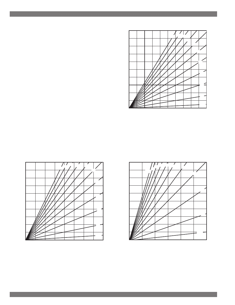
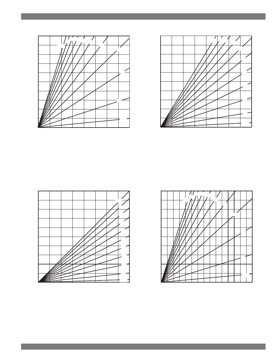
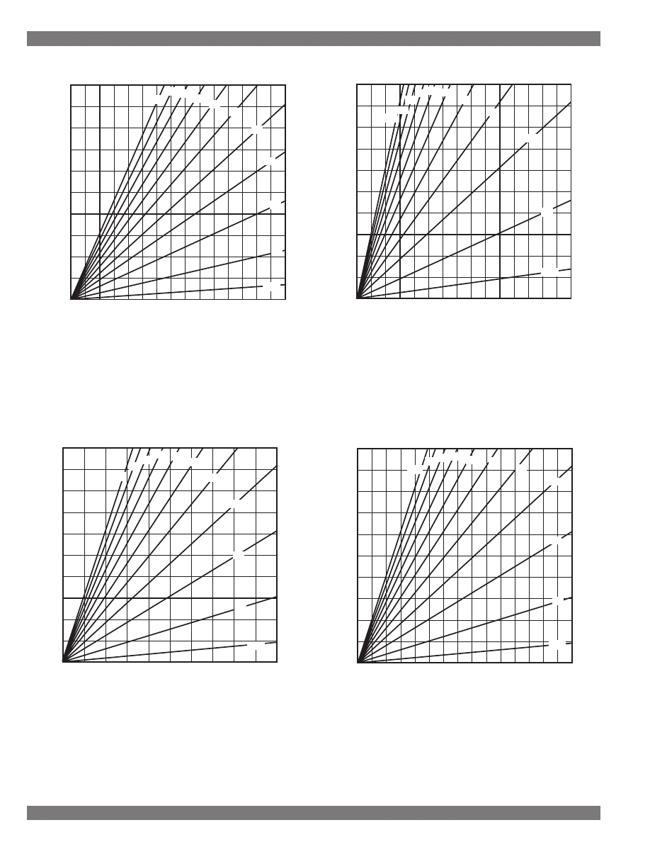
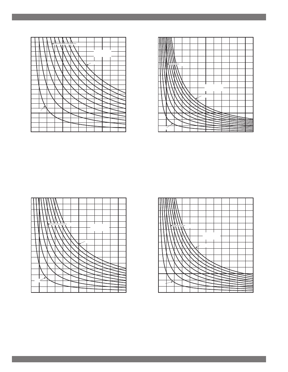
Output Current vs. Junction
Temperature and Voltage
Differential
(Figure 2-6)
These graphs show the junction temperature
with a given output current and input-output voltage
differential. Ambient temperature is 25
°
C. The ther-
mal resistance used for the calculations is shown
under each graph. This resistance assumes that a
heat sink of suitable size for the particular regulator
is employed; higher current regulator circuits gener-
ally require larger heat sinks. Refer to
Thermal Man-
agement, in Section 3, for definitions and details.
For example, a MIC5203-3.3BM4, supplying
50mA and with 6.3V on its input (V
IN
– V
OUT
= 3V), will
have a junction temperature of approximately 63
°
(Figure 2-6 (A)).
Figure 2-6 (A). SOT-143 with
θ
JA
= 250
°
C/W
Figure 2-6 (C). SOT-23-5 with
θ
JA
= 220
°
C/W
Figure 2-6 (B). SO-8 with
θ
JA
= 160
°
C/W
25
35
45
55
65
75
85
95
105
115
125
0
0.05
0.1
0.15
JUNCTION TEMPERATURE (
°
C)
OUTPUT CURRENT (A)
MIC5205
4V
5V
6V
7V
8V
9V
10V
3V
2V
1V
0.3V
Designing With LDO Regulators
19
Section 2: Design Charts
Micrel Semiconductor
Designing With LDO Regulators
25
35
45
55
65
75
85
95
105
115
125
0
0.05
0.1
0.15
0.2
JUNCTION TEMPERATURE (
°
C)
OUTPUT CURRENT (A)
MIC5201BM
4V
5V
6V
7V
8V
9V
10V
3V
2V
1V
0.3V
25
35
45
55
65
75
85
95
105
115
125
0
0.05
0.1
0.15
0.2
JUNCTION TEMPERATURE (
°
C)
OUTPUT CURRENT (A)
MIC5201BS
4V
5V
6V
7V
8V
9V
10V
3V
2V
1V
0.3V
25
35
45
55
65
75
85
95
105
115
125
0
0.05
0.10
0.15
0.20
0.25
0.30
0.35
0.40
JUNCTION TEMPERATURE (
°
C)
OUTPUT CURRENT (A)
MIC2920
4V
5V
6V
7V
8V
9V
10V
3V
2V
1V
0.3V
25
35
45
55
65
75
85
95
105
115
125
0
0.05
0.10
0.15
0.20
0.25
0.30
0.35
0.40
0.45
0.50
0.55
0.60
0.650.70
0.75
JUNCTION TEMPERATURE (
°
C)
OUTPUT CURRENT (A)
MIC2937ABU
4V
5V
6V
7V
8V
9V
10V
3V
2V
1V
0.3V
Figure 2-6 (D). High Current SO-8
with
θ
JA
= 160
°
C/W
Figure 2-6 (F). TO-263 with
θ
JA
= 40
°
C/W
Figure 2-6 (G). TO-263 with
θ
JA
= 40
°
C/W
Figure 2-6 (E). SOT-223 with
θ
JA
= 50
°
C/W
Micrel Semiconductor
Designing With LDO Regulators
Section 2: Design Charts
20
Designing With LDO Regulators
25
35
45
55
65
75
85
95
105
115
125
0
0.5
1.0
1.5
2.0
2.5
3.0
3.5
4.0
4.5
5.0
JUNCTION TEMPERATURE (
°
C)
OUTPUT CURRENT (A)
MIC29500
1V
0.3V
2V
3V
4V
5V
6V
7V
8V
9V
10V
25
35
45
55
65
75
85
95
105
115
125
0
0.1 0.2 0.3 0.4 0.5 0.6 0.7 0.8 0.9
1
1.1 1.2 1.3 1.4 1.5
JUNCTION TEMPERATURE (
°
C)
OUTPUT CURRENT (A)
MIC29150
4V
5V
6V
7V
8V
9V
10V
3V
2V
1V
0.3V
25
35
45
55
65
75
85
95
105
115
125
0
0.5 1.0 1.5 2.0 2.5 3.0 3.5 4.0 4.5 5.0 5.5 6.0 6.5 7.0 7.5
JUNCTION TEMPERATURE (
°
C)
OUTPUT CURRENT (A)
MIC29710
1V
0.3V
2V
3V
4V
5V
6V
7V
8V
9V
10V
25
35
45
55
65
75
85
95
105
115
125
0
0.5 1.0 1.5 2.0 2.5 3.0 3.5 4.0 4.5 5.0 5.5 6.0 6.5 7.0 7.5
JUNCTION TEMPERATURE (
°
C)
OUTPUT CURRENT (V)
MIC29750
4V
5V
6V
7V
8V
9V
10V
3V
2V
1V
0.3V
Figure 2-6 (H). TO-220 with
θ
JA
= 15
°
C/W
Figure 2-6 (K). TO-220 with
θ
JA
= 6
°
C/W
Figure 2-6 (L). TO-247 with
θ
JA
= 4
°
C/W
Figure 2-6 (J). TO-220 with
θ
JA
= 6
°
C/W
Designing With LDO Regulators
21
Section 2: Design Charts
Micrel Semiconductor
Designing With LDO Regulators
0
0.01
0.02
0.03
0.04
0.05
0.06
0.07
0.08
0
1
2
3
4
5
6
7
8
9
10
11
12
13
14
OUTPUT CURRENT (A)
V
IN
– V
OUT
MIC5203BM4
10
°
100
°
10
°
steps,
units in
°
C.
50
°
0
0.01
0.02
0.03
0.04
0.05
0.06
0.07
0.08
0.09
0.10
0.11
0.12
0.13
0.14
0.15
0
1
2
3
4
5
6
7
8
9
10
11
12
13
14
OUTPUT CURRENT (A)
V
IN
– V
OUT
MIC5205BM5
50
°
10
°
100
°
10
°
steps,
units in
°
C.
0
0.02
0.04
0.06
0.08
0.10
0.12
0.14
0.16
0.18
0.20
0
2
4
6
8
10
12
14
16
18
20
22
24
OUTPUT CURRENT (A)
V
IN
– V
OUT
MIC5201BM
100
°
10
°
steps,
units in
°
C.
50
°
10
°
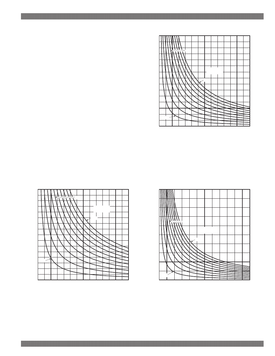
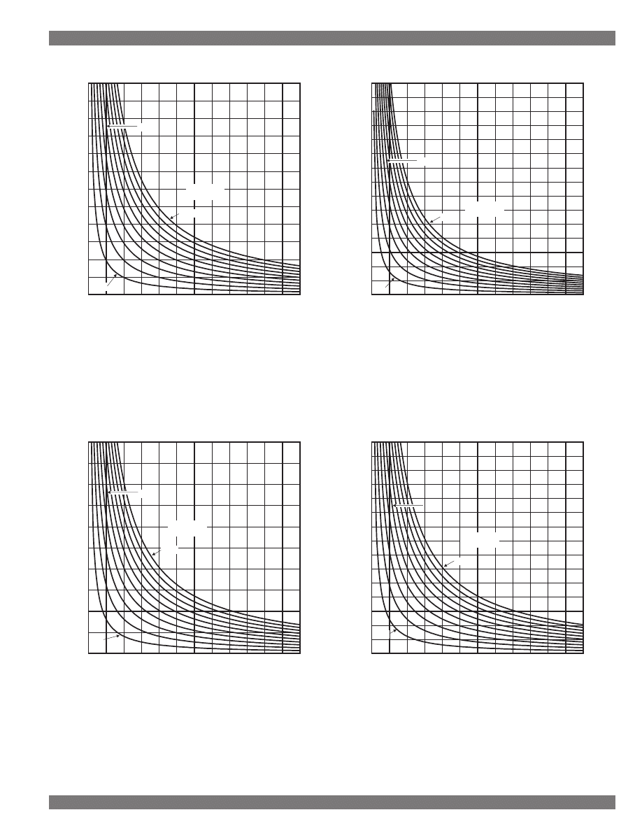
Junction Temperature Rise vs.
Available Output Current
and Differential Voltage
(Figure 2-7)
These graphs show the available thermally-lim-
ited steady-state output current with a given thermal
resistance and input—output voltage differential. The
assumed
θ
JA
(thermal resistance from junction to
ambient) is shown below each graph. Refer to
Ther-
mal Management in Section 3 for definitions and
details.
For example, Figure 2-7 (C) shows that the
MIC5205BM5, with 3V across it (V
IN
= V
OUT
+ 3V) and
supplying 120mA, will have a temperature rise of 80
°
C
(when mounted normally).
Figure 2-7 (C). SOT-23-5 with
θ
JA
= 220
°
C/W
Figure 2-7 (A). SOT-143 with
θ
JA
= 250
°
C/W
Figure 2-7 (D). SO-8 with
θ
JA
= 140
°
C/W
Micrel Semiconductor
Designing With LDO Regulators
Section 2: Design Charts
22
Designing With LDO Regulators
0
0.05
0.10
0.15
0.20
0.25
0.30
0.35
0.40
0
2
4
6
8
10
12
14
16
18
20
22
24
OUTPUT CURRENT (A)
V
IN
– V
OUT
MIC2920A
10
°
steps,
units in
°
C.
100
°
50
°
10
°
0
0.1
0.2
0.3
0.4
0.5
0.6
0.7
0.8
0.9
1.0
1.1
1.2
1.3
1.4
1.5
0
2
4
6
8
10
12
14
16
18
20
22
24
OUTPUT CURRENT (A)
V
IN
– V
OUT
MIC29150
100
°
10
°
steps,
units in
°
C.
10
°
50
°
0
0.05
0.10
0.15
0.20
0.25
0.30
0.35
0.40
0.45
0.50
0.55
0.60
0.65
0.70
0.75
0
2
4
6
8
10
12
14
16
18
20
22
24
OUTPUT CURRENT (A)
V
IN
– V
OUT
MIC2937A
10
°
steps,
units in
°
C.
100
°
50
°
10
°
0
0.02
0.04
0.06
0.08
0.10
0.12
0.14
0.16
0.18
0.20
0
2
4
6
8
10
12
14
16
18
20
22
24
OUTPUT CURRENT (A)
V
IN
– V
OUT
MIC5201BS
100
°
10
°
steps,
units in
°
C.
50
°
10
°
Figure 2-7 (E). SOT-223 with
θ
JA
= 50
°
C/W
Figure 2-7 (G). TO-263 with
θ
JA
= 40
°
C/W
Figure 2-7 (F). TO-263 with
θ
JA
= 40
°
C/W
Figure 2-7 (H). TO-220 with
θ
JA
= 15
°
C/W
Designing With LDO Regulators
23
Section 2: Design Charts
Micrel Semiconductor
Designing With LDO Regulators
0.0
0.5
1.0
1.5
2.0
2.5
3.0
3.5
4.0
4.5
5.0
5.5
6.0
6.5
7.0
7.5
0
2
4
6
8
10
12
14
16
18
20
22
24
OUTPUT CURRENT (A)
V
IN
– V
OUT
MIC29710
10
°
steps,
units in
°
C.
50
°
100
°
10
°
0.0
0.5
1.0
1.5
2.0
2.5
3.0
3.5
4.0
4.5
5.0
5.5
6.0
6.5
7.0
7.5
0
2
4
6
8
10
12
14
16
18
20
22
24
OUTPUT CURRENT (A)
V
IN
– V
OUT
MIC29750
10
°
100
°
10
°
steps,
units in
°
C.
50
°
0
0.5
1.0
1.5
2.0
2.5
3.0
3.5
4.0
4.5
5.0
0
2
4
6
8
10
12
14
16
18
20
22
24
OUTPUT CURRENT (A)
V
IN
– V
OUT
MIC29500
50
°
100
°
10
°
steps,
units in
°
C.
10
°
0
0.5
1.0
1.5
2.0
2.5
3.0
0
2
4
6
8
10
12
14
16
18
20
22
24
OUTPUT CURRENT (A)
V
IN
– V
OUT
MIC29300
100
°
10
°
steps,
units in
°
C.
50
°
10
°
Figure 2-7 (I). TO-220 with
θ
JA
= 10
°
C/W
Figure 2-7 (K). TO-220 with
θ
JA
= 6
°
C/W
Figure 2-7 (L). TO-247 with
θ
JA
= 4
°
C/W
Figure 2-7 (J). TO-220 with
θ
JA
= 6
°
C/W

Micrel Semiconductor
Designing With LDO Regulators
Section 3: Using LDO Linear Regulators
24
Designing With Linear Regulators
Section 3. Using LDO Linear Regulators
Output Capacitor
The Super
β
eta PNP regulators require a cer-
tain minimum value of output capacitance for opera-
tion—below this minimum value, the output may ex-
hibit oscillation. The output capacitor is inside the
voltage control loop and is necessary for loop stabili-
zation. Minimum recommended values are listed on
each device data sheet. There is
no maximum value—
the output capacitor may be increased without limit.1
Excellent response to high frequency load
changes (load current transient recovery) demands
low inductance, low ESR, high frequency filter ca-
pacitors. Stringent requirements are solved by paral-
leling multiple medium sized capacitors. Capacitors
should be chosen by comparing their lead inductance,
ESR, and dissipation factor. Multiple small or medium
sized capacitors provide better high frequency char-
acteristics than a single capacitor of the same total
capacity since the lead inductance and ESR of the
multiple capacitors is reduced by paralleling.
Although the capacitance value of the filter may
be increased without limit, if the ESR of the paral-
leled capacitors drops below a certain (device family
dependent) threshold, a zero in the transfer plot ap-
pears, lowering phase margin and decreasing stabil-
ity. With some devices, especially the MIC5157 and
MIC5158 Super LDO, this problem is solved by us-
ing a low ESR input decoupling capacitor. Worst-case
situations may require changes to higher ESR out-
put capacitors—perhaps increasing both the ESR and
the capacitance by using a different chemistry—or,
as a last resort, by adding a small series resistance
( < 1
Ω
) between the regulator and the capacitor(s).
General Layout and
Construction␣ Considerations
Layout
Although often considered “just a D.C. Circuit”,
low-dropout linear regulators are actually built with
moderately high frequency transistors because rapid
response to input voltage or output current changes
demand excellent high frequency performance. These
characteristics place some requirements on bypass
capacitors and board layout.
Bypass Capacitors
Low-dropout linear regulators need capacitors
on both their input and output. The input capacitor
provides bypassing of the internal op amp used in
the voltage regulation loop. The output capacitor im-
proves regulator response to sudden load changes,
and in the case of the Super
β
eta PNP™ devices,
provides loop compensation that allows stable op-
eration.
The input capacitor for monolithic regulators
should feature low inductance and generally good
high frequency performance. Capacitance is not too
critical except for systems where excessive input
ripple voltage is present. The capacitor must, as a
minimum, maintain the input voltage minimum value
above the dropout point. Otherwise, the regulator
ceases regulation and becomes merely a saturated
switch. In an AC-line powered system, where the regu-
lator is mounted within a few centimeters from the
main filter capacitor, additional capacitors are often
unnecessary. A 0.1
µ
F ceramic directly adjacent to the
regulator is always a good choice, however. If the
regulator is farther away from the filter capacitor, lo-
cal bypassing is mandatory.
With the high current MIC5157 and MIC5158
Super LDO™ regulator controllers, the input capaci-
tor should be a medium sized (10
µ
F or larger) low
ESR (effective series resistance) type.
NOTE 1: Truly huge output capacitors will extend the start-up
time, since the regulator must charge them. This time is
determined by capacitor value and the current limit value
of the regulator.
Designing With LDO Regulators
25
Section 3: Using LDO Linear Regulators
Micrel Semiconductor
Designing With LDO Regulators
Circuit Board Layout
Stray capacitance and inductance may upset
loop compensation and promote instability. Exces-
sive input lead resistance increases the dropout volt-
age, and excessive output lead resistance reduces
output load regulation. Ground loops also cause both
problems. Careful layout is the solution.
Reduce stray capacitance and inductance by
placing bypass and filter capacitors close to the regu-
lator. Swamp parasitic reactances by using a 0.1
µ
F
ceramic capacitor (or equivalent) in parallel with the
regulator input filter capacitor. Designers of battery-
powered circuits often overlook the finite high-fre-
quency impedance of their cells. The ceramic capaci-
tor solves many unexpected problems.
Excessive lead resistance, causing unwanted
voltage drops and ruining load regulation, is solved
by merely increasing conductor size. Regulators with
remote sensing capability—like all Micrel
adjustables—may utilize a Kelvin-sense connection
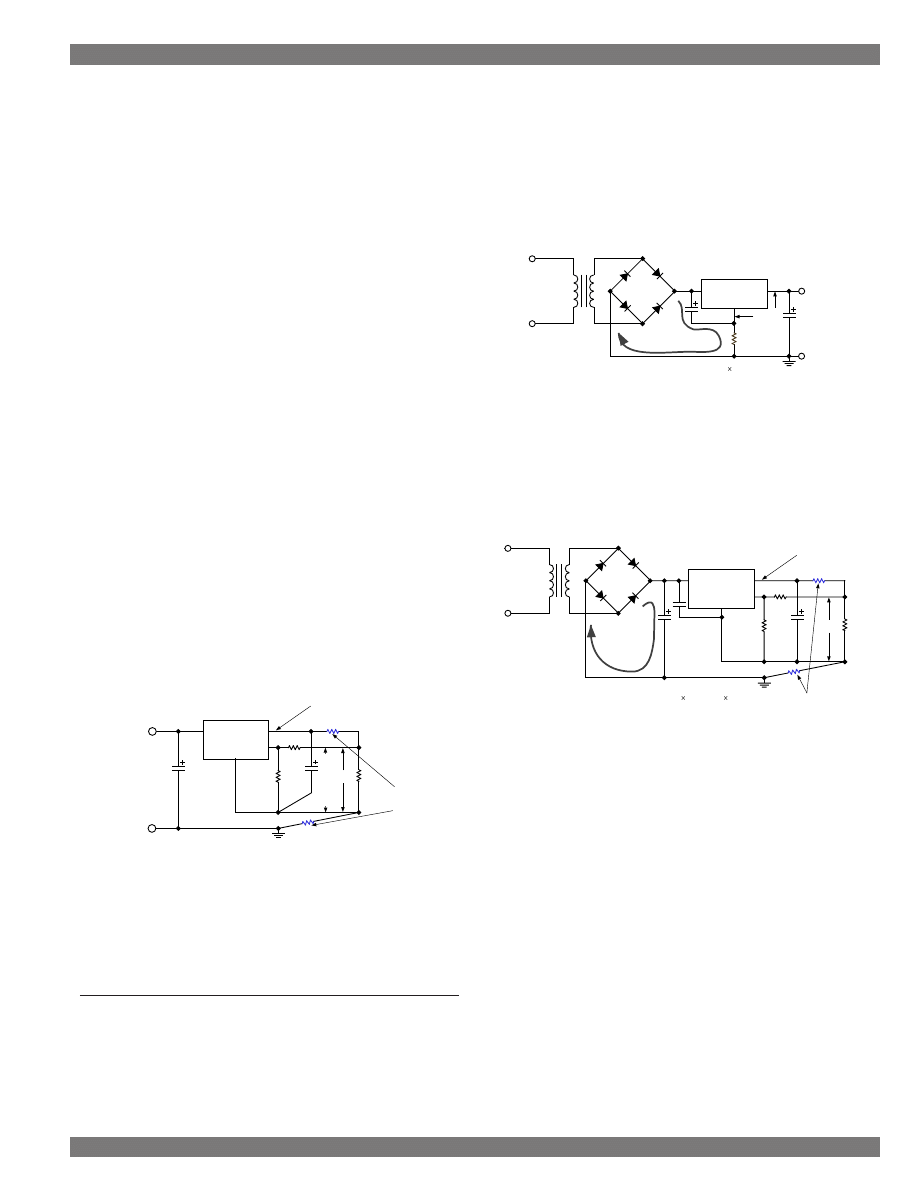
directly to the load. As Figure 3-1 shows, an addi-
tional pair of wires feeds back the load voltage to the
regulator sense input.2 This lets the regulator com-
pensate for line drop. As the Kelvin sense leads carry
only the small voltage-programming resistor current,
they may be very narrow traces or small diameter
wire. A judicious layout is especially important in re-
mote-sensed designs, since these long, high imped-
ance leads are susceptible to noise pickup.
VOUT
@
IDC OUT
Trace
Resistance
RL
R1
R2
ADJ
VREG
IN
OUT
GND
Remote Sense
VIN
GND
Figure 3-1. Remote Voltage Sense (Kelvin)
Connections
A common ground loop problem occurs when
rectifier ripple current flows through the regulator’s
ground lead on its way to the filter capacitor (see Fig-
ure 3-2). The ripple current, which is several times
larger than the average DC current, may create a
voltage drop in the ground line, raising its voltage rela-
tive to the load. As the regulator attempts to compen-
sate, load regulation suffers. Solve the problem by
ensuring rectifier current flows directly into the filter
capacitor.
AC Input
VOUT
@
IDC OUT
Low-Dropout
Linear Regulator
Ripple Current
Trace
Resistance
+
–
VOUT = VREG + (IRIPPLE RTRACE)
Where IRIPPLE >> IDC OUT
V REG
Figure 3-2. Ground Loop and Ripple Currents
Degrade Output Accuracy
Figure 3-3 shows an ideal layout for remote-
sensed loads. If a single point ground is not practical,
load regulation is improved by employing a large
ground plane.
AC Input
VOUT
@
IDC OUT
MIC29302
Ripple Current
Trace
Resistance
VOUT = VREG + (2 IDC OUT RTRACE)
RL
R1
R2
ADJ
0.1µF
VREG
Figure 3-3. Regulator Layout With Remote Voltage
Sensing
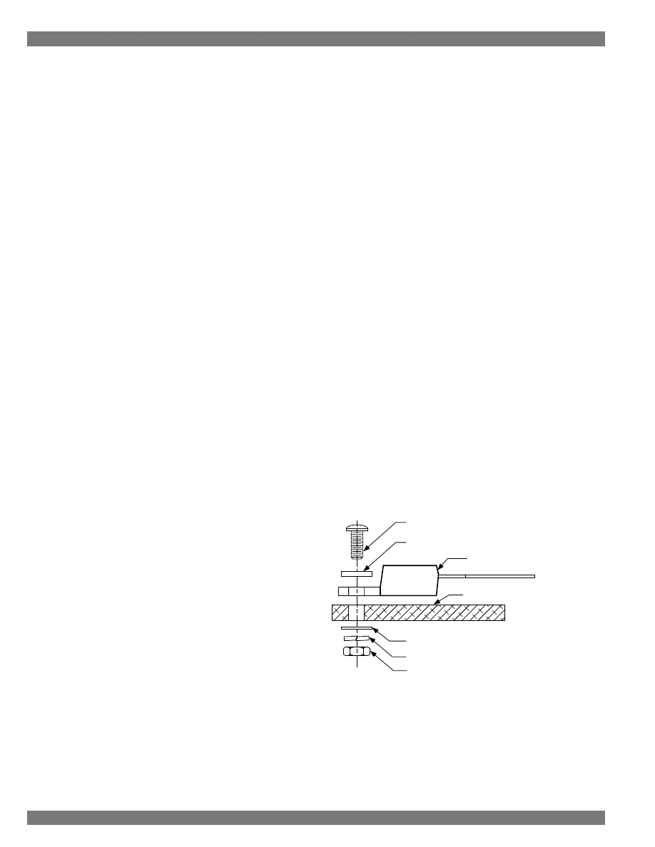
Assembly
Low power regulator circuits are built like any
other analog system. Surface mounted systems are
assembled using normal reflow (or similar), tech-
niques. Larger leaded packages may require special
lead bending before installation; specific lead bend
options are available from Micrel, or the assembler
may bend them. When power demands force the use
of a heat sink, extra care must be applied during as-
sembly and soldering. Our assembly discussion will
focus on the popular TO-220 package but it is gener-
ally applicable to other package types.
NOTE 2: The internal reference in most Micrel regulators is
positioned between the adjust pin and ground, unlike the
older “classic” NPN regulator designs. This technique,
while providing excellent performance with Micrel regu-
lators, does not work with the older voltage regulators; in
fact, it reduces their output voltage accuracy.
Micrel Semiconductor
Designing With LDO Regulators
Section 3: Using LDO Linear Regulators
26
Designing With Linear Regulators
Lead Bending
If lead bending is necessary, use the standard
bend options offered by Micrel whenever possible.
These bending operations are performed on tooling
developed specifically for this purpose and with the
safety of the package, die, and internal wire bonds in
mind. Custom lead bending is also available for a
nominal charge.
For prototyping or other low quantity custom lead
bending requirements, clamp the leads at the junc-
tion of the case with long nosed pliers. Using your
fingers or another pair of pliers, bend the outer lead
as desired. Please observe the following cautions:
•
Do not spread or compress the leads
•
Do not bend or twist the leads at the body junc-
tion: start the bend at least 3mm from the body
•
Maintain a lead bend radius of approximately
1mm
•
Do not re-bend leads multiple times
Micrel TO-220 packages are made from nickel-
plated or tinned copper for best electrical and ther-
mal performance. While rugged electrically, they are
susceptible to mechanical stress and fatigue. Please
handle them with care!
Heat Sink Attachment
TO-220 package applications at moderate
(room) temperatures may not require heat sinking if
the power dissipation is less than 2 watts. Otherwise,
heat sinks are necessary. Use the minimum practical
lead length so heat may travel more directly to the
board, and use the board itself as a heat sink.
Attachment techniques vary depending upon the
heat sink type, which in turn depends upon the power
dissipated. The first consideration is whether or not
electrical isolation is required. Micrel’s Super ßeta
PNP regulators all have a grounded tab, which usu-
ally means no insulation is necessary. This helps by
reducing or eliminating one of the thermal resistances.
Next, we determine heat sink size. See the
Thermal
Management chapter for details. If a standard com-
mercial heat sink is chosen, we may generally as-
sume minimal surface roughness or burrs.
Otherwise, machining the mounting pad may be
necessary to achieve a flatness (peak-to-valley) of 4
mils per inch with a surface finish of
±
1.5
µ
m or bet-
ter for minimum thermal resistance.
Holes for the mounting screw should be drilled
and deburred. Slightly oversized holes allow for slip-
page during temperature cycling and is generally rec-
ommended.
Heat sinks of bare aluminum or copper are not
optimum heat radiators. Anodizing or painting im-
proves heat radiation capability. For more details on
heat sinks, see the
References.
Thermal grease, thermal pads, or other thermally
conductive interface between the package and the
heat sink compensates for surface flatness errors,
mounting torque reduction over time, air gaps, and
other sins, and is recommended. Heat sink manu-
facturers offer a variety of solutions with widely vary-
ing prices, installation ease, and effectiveness.
Many heat sinks are available with mounting
clips. These allow fast assembly and, when the clip
also presses against the plastic body instead of only
the metal tab, provide excellent heat contact area and
low thermal resistance.
Machine screws are often used for heat sink at-
tachment (see Figure 3-4). Proper torque is impera-
tive; too loose and the thermal interface resistance is
excessive; too tight and the semiconductor die will
crack. The 0.68N-m specification applies to clean
threads; ensure that the thermal grease does not in-
terfere with the threads.
6-32 Hex Nut
#6 Lock Washer
#6 Flat Washer (Optional)
6-32 Phillips Pan Head Machine Screw
TO-220 Package
Maximum Torque: 0.68 N-m (6 in-lbs)
(Caution: Excessive torque may crack semiconductor)
Apply Heat-Transfer Compound
Between Surfaces
#6 Nylon Flat Washer
Figure 3-4. Mounting TO-220 Packages
to Heat Sinks
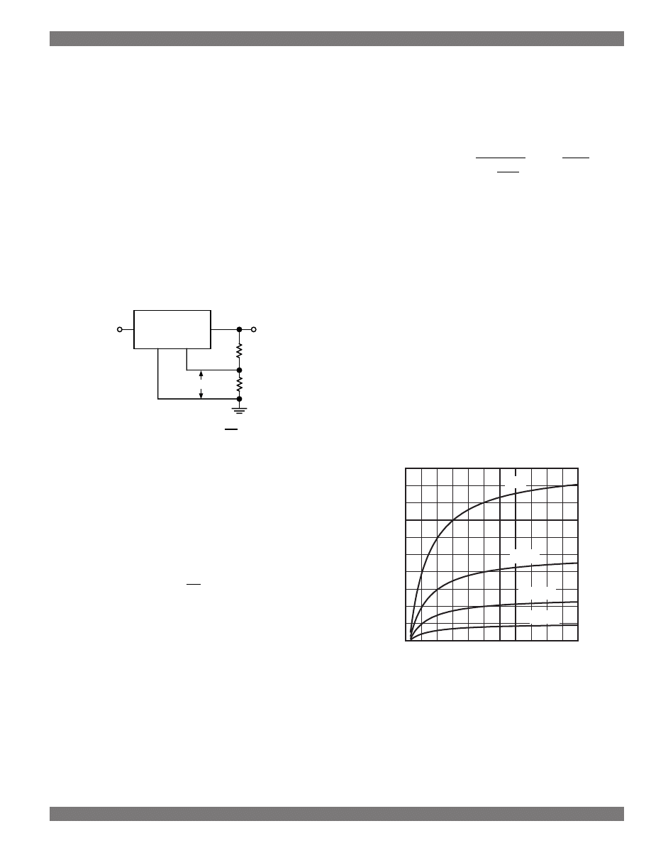
Designing With LDO Regulators
27
Section 3: Using LDO Linear Regulators
Micrel Semiconductor
Designing With LDO Regulators
Output Voltage Accuracy
Adjustable Regulator Accuracy Analysis
Micrel LDO Regulators are high accuracy de-
vices with output voltages factory-trimmed to much
better than 1% accuracy. Across the operating tem-
perature, input voltage, and load current ranges, their
worst-case accuracies are still better than
±
2%. For
adjustable regulators, the output also depends upon
the accuracy of two programming resistors. Some
systems require supply voltage accuracies better than
±
2.5%—including noise and transients. While noise
is generally not a major contributor to output inaccu-
racy, load transients caused by rapidly varying loads
(such as high-speed microprocessors), are significant,
even when using fast transient-response LDO regu-
lators and high-quality filter capacitors.
Micrel Adjustable
Regulator
1.24V
V
OUT
V
IN
ADJ
GND
R1
R2
VOUT = 1.240
×
(1+ )
R1
R2
Figure 3-5. An adjustable linear regulator uses the
ratio of two resistors to determine its output voltage.
Adjustable regulators use the ratio of two resis-
tors to multiply the reference voltage to produce the
desired output voltage (see Figure 3-5). The formula
for output voltage from two resistors is presented as
Equation 3-1.
(3-1)
V
= V
1
R1
R2
OUT
REF
+
The basic MIC29512 has a production-trimmed
reference (VREF) with better than
±
1% accuracy at a
fixed temperature of 25
°
C. It is guaranteed better than
±
2% over the full operating temperature range, input
voltage variations, and load current changes. Since
practical circuits experience large temperature swings
we should use the
±
2% specification as our theoreti-
cal worst-case. This value assumes no error contri-
bution from the programming resistors.
Referring to Figure 3-5 and Equation 3-1, we
see that resistor tolerance (tol) must be added to the
reference tolerance to determine the total regulator
inaccuracy. A sensitivity analysis of this equation
shows that the error contribution of the adjust resis-
tors is:
(3-2)
Error
Contribution
% =
2
tol%
1
tol%
100
1
V
V
REF
OUT
×
−
×
−
Since the output voltage is proportional to the
product of the reference voltage and the ratio of the
programming resistors, at high output voltage, the
error contribution of the programming resistors is the
sum of each resistor’s tolerance. Two standard
±
1%
resistors contribute as much as 2% to output voltage
error. At lower voltages, the error is less significant.
Figure 3-6 shows the effects of resistor tolerance on
regulator accuracy from the minimum output voltage
(VREF) to 12V. At the minimum VOUT, theoretical
resistor tolerance has no effect on output accuracy.
Resistor error increases proportionally with output
voltage: at an output of 2.5V, the sensitivity factor is
0.5; at 5V it is about 0.75; and at 12V it is over 0.9.
This means that with 5V of output, the error contribu-
tion of 1% resistors is 0.75 times the sum of the toler-
ances, or 0.75
×
2% = 1.5%. As expected, more pre-
cise resistors offer more accurate performance.
0
0.2
0.4
0.6
0.8
1.0
1.2
1.4
1.6
1.8
2.0
1 2 3 4 5 6 7 8 9 10 11 12
ERROR PERCENTAGE
OUTPUT VOLTAGE
1%
0.5%
0.25%
0.1%
Figure 3-6. Resistor Tolerance Effects on
Adjustable Regulator Accuracy
The output voltage error of the entire regulator
system is the sum of reference tolerance and the re-
sistor error contribution. Figure 3-7 shows this worst-
case tolerance for the MIC29512 as the output volt-
Micrel Semiconductor
Designing With LDO Regulators
Section 3: Using LDO Linear Regulators
28
Designing With Linear Regulators
age varies from minimum to 12V using
±
1%,
±
0.5%,
±
0.25%, and
±
0.1% resistors. The more expensive,
tighter accuracy resistors provide improved tolerance,
but it is still limited by the adjustable regulator’s
±
2%
internal reference.
0
0.2
0.4
0.6
0.8
1.0
1.2
1.4
1.6
1.8
2.0
1 2 3 4 5 6 7 8 9 10 11 12
ERROR PERCENTAGE
OUTPUT VOLTAGE
1%
0.5%
0.25%
0.1%
Figure 3-7. Worst-Case Output Tolerance
A better method is possible: increase the overall
accuracy of the regulator by employing a precision
reference in the feedback loop.
Improving Regulator Accuracy
Achieving a worst-case error of
±
2.5%, includ-
ing all D/C and A/C error terms, is possible by in-
creasing the basic accuracy of the regulator itself, but
this is expensive since high current regulators have
significant self-heating. Its internal reference must
maintain accuracy across a wide temperature range.
Testing for this level of performance is time consum-
ing and raises the cost of the regulator, which is un-
acceptable for extremely price-sensitive marketplaces.
Some systems require better than
±
2% accuracy. This
high degree of accuracy is possible using Micrel's
LM4041 voltage reference instead of one of the pro-
gramming resistors (refer to Figure 3-8). The regula-
tor output voltage is the sum of the internal reference
and the LM4041’s programmed voltage (Equation
3-3).
(3-3)
VOUT = VREF Regulator + VLM4041
= 1.240 + VLM4041
The benefit of this circuit is the increased accu-
racy possible by eliminating the multiplicative effect
of the regulator’s internal reference. In normal con-
figurations, the reference error is multiplied up by the
resistor ratio, keeping the error percentage constant.
With this circuit, the error voltage is within 25mV, ab-
solute. Another benefit of this arrangement is that the
LM4041 is not a dissipative device: there is only a
small internal temperature rise to degrade accuracy.
Additionally, both references are operating in their low-
sensitivity range so we get less error contribution from
the resistors. A drawback of this configuration is that
the minimum output voltage is now the sum of both
references, or about 2.5V. The adjustable LM4041 is
available in accuracies of
±
0.5% and
±
1%, which al-
lows better overall system output voltage accuracy.
Equation 3-4 presents the formula for the
LM4041-ADJ output voltage. Note the output voltage
has a slight effect on the reference. Refer to the
LM4040 data sheet for full details regarding this sec-
ond-order coefficient.
(3-4)
V
V
V
V
1.233
R1b
R1a
1
LM4041
OUT
REF
OUT
=
×
+
×
+
∆
∆
Actually, the voltage drop across R1b is slightly
higher than that calculated from Equation 3-4. Ap-
proximately 60nA of current flows out of the LM4041
FB terminal. With large values of R1b, this current
creates millivolts of higher output voltage; for best
accuracy, compensate R1b by reducing its size ac-
cordingly. This error is +1mV with R1b = 16.5k
Ω
.
Equation 3-5 shows the nominal output voltage for
the composite regulator of Figure 4.
(3-5)
V
1.233
R1b
R1a
1
1.0013
0.0013R1b
R1a
60nA R1b
1.240
OUT
=
+
+
×
(
)
+
Note that the tolerance of R2 has no effect on
output voltage accuracy. It sets the diode reverse (op-
erating) current and also allows the divider current
from R1a and R1b to pass. With R2 = 1.2k
Ω
, 1mA of
bias flows. If R2 is too small (less than about 105
Ω
,
the maximum reverse current of the LM4041-ADJ is
exceeded. If it is too large with respect to R1a and
R1b then the circuit will not regulate. The recom-
mended range for R2 is from 121
Ω
to
R1a
⁄
10
.
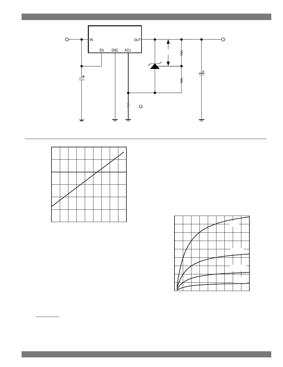
Designing With LDO Regulators
29
Section 3: Using LDO Linear Regulators
Micrel Semiconductor
Designing With LDO Regulators
Figure 3-10 shows the resistor error contribu-
tion to the LM4041C reference output voltage toler-
ance. Figure 3-11 shows the worst-case output volt-
age error of the composite regulator circuit using vari-
ous resistor tolerances, when a 0.5% LM4041C ref-
erence is employed. The top four traces reflect use
of 1%, 0.5%, 0.25%, and 0.1% resistors. Table 3-1
lists the production accuracy obtained with the low-
cost LM4041C and standard 1% resistors as well as
the improvement possible with 0.1% resistors.
0
0.7
0.9
1.1
1.3
1.5
1.7
1.9
2.1
2.3
1
2
3
4
5
6
7
8
9 10
ERROR PERCENTAGE
OUTPUT VOLTAGE
1%
0.25%
0.1%
0.5%
Figure 3-10. Resistor Tolerance Effects on LM4041
Voltage Reference Accuracy
Figure 3-8. Improved Accuracy Composite Regulator Circuit
0
2
4
6
8
10
12
0
100
200
300
400
500
600
700
800
900
OUTPUT VOLTAGE (V)
RESISTOR R1b (k
Ω
)
Figure 3-9. Output Voltage vs. R1b
(See Figure 3-8)
Regulator & Reference Circuit
Performance
With this circuit we achieve much improved ac-
curacies. Our error terms are:
25mV
(constant) from the MIC29512
0.5%
from the LM4041C
+ 0 to 2%
from R1a and R1b
0.5% + 25mV to
Total Error Budget
2.5% + 25mV
MIC29512BT
MIC29712BT
R2
330
(tolerance not critical)
R1a
120k
Ω
R1b
LM4041-ADJ
VIN
VOUT
1.233V
Micrel Semiconductor
Designing With LDO Regulators
Section 3: Using LDO Linear Regulators
30
Designing With Linear Regulators
Composite
Standard
VOUT
Circuit
Circuit
2.50V
±
1.6%
±
3.0%
3.00V
±
1.9%
±
3.2%
3.30V
±
2.1%
±
3.3%
3.50V
±
2.1%
±
3.2%
5.00V
±
2.4%
±
3.5%
6.00V
±
2.4%
±
3.6%
8.00V
±
2.5%
±
3.7%
10.00V
±
2.5%
±
3.8%
11.00V
±
2.5%
±
3.8%
Table 3-2. Comparing the Worst-Case Output
Voltage Error for the Two Topologies With
Typical Output Voltages
0
0.7
0.9
1.1
1.3
1.5
1.7
1.9
2.1
2.3
2.5
2.5
3.5
4.5
5.5
6.5
7.5
8.5
9.5
10.5
11.5
ERROR PERCENTAGE
OUTPUT VOLTAGE
1%
0.1%
0.25%
0.5%
Figure 3-11. Composite Regulator Accuracy
What does the extra complexity of the compos-
ite regulator circuit of Figure 3-8 buy us in terms of
extra accuracy? With precision components, we may
achieve tolerances better than
±
1% with the compos-
ite regulator, as compared to a theoretical best case
of somewhat worse than 2% with the standard regu-
lator and resistor configuration. Figure 3-12 and Table
VOUT
1% Resistors
0.1% Resistors
2.50V
±
1.54%
±
1.50%
2.90V
±
1.88%
±
1.41%
3.00V
±
1.94%
±
1.39%
3.30V
±
2.07%
±
1.34%
3.45V
±
2.12%
±
1.31%
3.525V
±
2.14%
±
1.30%
3.60V
±
2.16%
±
1.29%
5.00V
±
2.36%
±
1.13%
6.00V
±
2.41%
±
1.07%
8.00V
±
2.46%
±
0.98%
10.00V
±
2.49%
±
0.92%
11.00V
±
2.49%
±
0.90%
Table 3-1. Worst-Case Output Voltage Error for
Typical Operating Voltages Using the LM4040C
(
±
0.5% Accuracy Version)
3-2 show the accuracy difference between the cir-
cuits as the output voltage changes. The accuracy
difference is the tolerance of the two-resistor circuit
minus the tolerance of the composite circuit. Both tol-
erances are the calculated worst-case value, using
1% resistors. This figure shows the composite circuit
is always at least 1% better than the standard con-
figuration. Both the figure and the table assume stan-
dard
±
1% resistors and the LM4041C-ADJ (0.5%) ref-
erence.
0
0.2
0.4
0.6
0.8
1.0
1.2
1.4
1.6
1.8
2.0
2
3
4
5
6
7
8
9 10 11 12
Accuracy Difference (%)
OUTPUT VOLTAGE (V)
y
Figure 3-12. Accuracy difference between the
Standard Two-Resistor Circuit and the Composite
Circuit of Figure 3-8
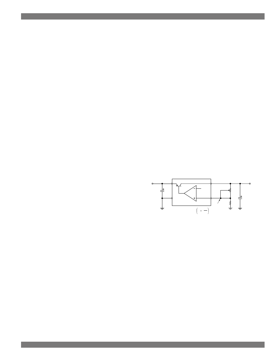
Designing With LDO Regulators
31
Section 3: Using LDO Linear Regulators
Micrel Semiconductor
Designing With LDO Regulators
Design Issues and
General␣ Applications
Noise and Noise Reduction
Most of the output noise caused by a LDO regu-
lator emanates from the voltage reference. While
some of this noise may be shunted to ground by the
output filter capacitor, bypassing the reference at a
high impedance node provides more attenuation for
a given capacitor value. The MIC5205 and MIC5206
use a lower noise bandgap reference and also pro-
vide external access to this reference. A small value
(470pF or so) external capacitor attenuates output
noise by about 10dB for a 5 volt output.
All of Micrel’s adjustable regulators allow a simi-
lar technique. By shunting one of the voltage program-
ming resistors with a small-value capacitor, the high
frequency gain of the regulator is reduced which
serves to reduce high frequency noise. The capaci-
tor should be placed across the resistor connecting
between the feedback pin and the output (R1 on data
sheet schematics).
Stability
Low dropout linear regulators with a PNP out-
put require an output capacitor for stable operation.
See
Stability Issues in Section 4, Linear Regulator
Solutions for a discussion on stability with Super
β
eta
PNP regulators.
The Super LDO is more stable than the mono-
lithic devices and rarely needs much attention to guar-
antee stability.
Micrel’s Unique “Super LDO”, also in
Section 4, discusses the few parameters requiring
vigilance.
LDO Efficiency
The electrical efficiency of all electronic devices
is defined as POUT
÷
PIN. A close efficiency approxi-
mation for linear regulators is
VOUT
Eff =
———
VIN
This approximation neglects regulator operating
current, but is very accurate (usually within 1%) for
Super
β
eta PNP and Super LDO regulators with their
very low housekeeping power draw. The full formula
is:
VIN
×
(IGND) + (VIN – VOUT)
×
IOUT
Eff = —————————————————
VOUT
×
IOUT
Building an Adjustable Regulator
Allowing 0V Output
Some power supplies, especially laboratory
power supplies and power systems demanding well-
controlled surge-free start-up characteristics, require
a zero-volt output capability. In other words, an ad-
justable laboratory power supply should provide a
range than includes 0V. However, as shown in Fig-
ure 3-13, a typical adjustable regulator does not fa-
cilitate adjustment to voltages lower than VREF (the
internal bandgap voltage). Adjustable regulator ICs
are designed for output voltages ranging from their
reference voltage to their maximum input voltage
(minus dropout); the reference voltage is generally
about 1.2V. The lowest output voltage available from
this circuit is provided when R1 = 0
Ω.
For the
MIC29152 LDO regulator, VREF = 1.240V, so
VOUT(min) = VREF(1+R1/R2), or 1.240V.
Typical LDO Regulator
V
REF
V
OUT
R1
2M
Ω
1%
R2
102k
Ω
1%
V
ADJ
OUT
IN
GND
C
IN
22µF
ADJ
MIC29152
V
IN
C
OUT
22µF
(1.24 – 25V)
(26V)
V
OUT (max)
= V
REF
1
R1
R2
Figure 3-13. Typical Adjustable Regulator
Two designs work around the minimum output
voltage limitation. The first uses a low-cost reference
diode to create a “virtual” VOUT that cancels the ref-
erence. The second uses op-amps to convince the
regulator adjust pin that zero volts is a proper output
level. In both cases, the feedback-loop summing junc-
tion must be biased at VREF to provide linear opera-
tion.
Reference Generates a “Virtual VOUT”
Figure 3-14 shows a simple method of achiev-
ing a variable output laboratory supply or a less-than-
1.2V fixed-output supply. The circuit uses a second
bandgap reference to translate the regulator’s output
up to a “virtual VOUT” and then uses that virtual VOUT
as the top of a feedback divider. The output voltage
adjusts from 0V to about 20V.
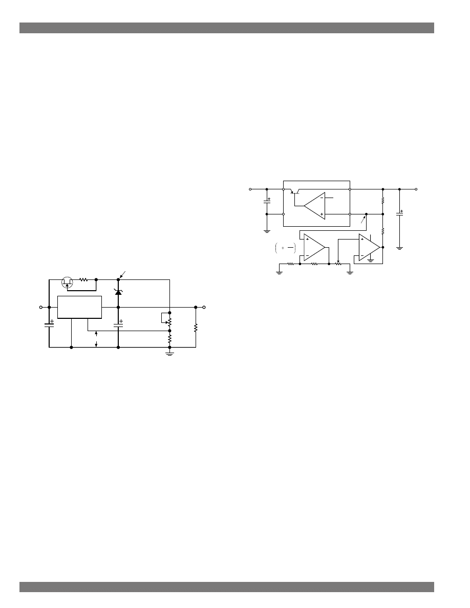
Micrel Semiconductor
Designing With LDO Regulators
Section 3: Using LDO Linear Regulators
32
Designing With Linear Regulators
When R1 goes to 0
Ω
, the output is about 0V,
the virtual VOUT is one bandgap voltage above
ground, and the adjust input is also one bandgap
voltage above ground. The regulator’s error amplifier
loop is satisfied that both of its inputs are at one
bandgap voltage and it keeps the output voltage con-
stant at 0V. The virtual VOUT tracks any increases in
R1, remaining one bandgap voltage above the ac-
tual VOUT, as the output rises from ground. The maxi-
mum possible VOUT equals the regulator’s maximum
input voltage minus the approximately 2V housekeep-
ing voltage required by the current-source FET and
the external bandgap reference.
The current source, composed of a 2N3687
JFET and R3, is designed for about 77
µ
A. Seven
microamperes for the resistor string (about 100 times
the nominal 60nA input current of the regulator’s ad-
just input) and 70
µ
A for the bandgap. R2 is optional,
and is needed only if no load is present. It bleeds off
the 70
µ
A of reference current and satisfies the mini-
mum load current requirement of the regulator.
MIC29152BT
1.24V
V
OUT
0V to 20V
V
IN
ADJUST
LM4041DIM3-1.2
BANDGAP
REFERENCE
R1
3M
180k
R2
620
2N3697 R3
8k
VIRTUAL V
OUT
Figure 3-14. Adjust to Zero Volt Circuit Using
a Reference Diode
A drawback of this simple design is that the volt-
age of the internal reference in the regulator must
match the external (LM4041) voltage for the output
to actually reach zero volts. In practice, the minimum
output voltage from this simple circuit is a few milli-
volts.
Op-Amp Drives Ground Reference
The circuit of Figure 3-15 provides adjustability
down to 0V by controlling the ground reference of the
feedback divider. It uses the regulator’s internal
bandgap reference to provide both accuracy and
economy. Non-inverting amplifier A2 senses VREF
(via VADJ) and provides a gain of just slightly more
than unity. When R5 is adjusted to supply ground to
voltage follower A1 then ground is also applied to the
bottom of feedback voltage divider R1 and R2, and
operation is identical to the standard adjustable regu-
lator configuration, shown in Figure 3-13 (when ad-
justed to provide maximum output voltage). Con-
versely, when R5 is adjusted so the input to voltage
follower A1 is taken directly from the output of ampli-
fier A2 the bottom of voltage divider R1 and R2 is
biased such that VADJ will equal VREF when VOUT
is 0V. Rotation of R5 results in a smooth variation of
output voltage from 0V to the upper design value,
which is determined by R1 and R2.
Typical LDO Regulator
V
REF
V
OUT
R1
2M
Ω
1%
R2
102k
Ω
1%
V
ADJ
OUT
IN
GND
C
IN
22µF
ADJ
MIC29152
V
IN
C
OUT
22µF
(0V–25V)
(26V)
5
6
4
V
IN
8
3
2
R5
100K
Ω
R4
102k
Ω
1%
R3
2M
Ω
1%
A2
1/2 LM358
A1
1/2 LM358
7
R3 = R1 and R4 = R2
V
OUT (max)
= V
REF
1
R1
R2
Figure 3-15. 0V-to-25V Adjustable Regulator
The gain of amplifier A2 is 1 + R4 / R3 = 1.05, in
this example. Note that the portion of gain above unity
is the reciprocal of the attenuation ratio afforded by
feedback divider R1 and R2; i.e., R4 / R3 = 1 / (R1 /
R2) To provide optimal ratio matching, resistors R3
and R4 have been chosen to be the same values
and types as their counterparts R1 and R2, respec-
tively.
Systems With Negative Supplies
A common start-up difficulty occurs if a regula-
tor output is pulled below ground. This is possible in
systems with negative power supplies. An easy fix is
shown in Figure 3-16: adding a power diode, such as
a 1N4001, from the regulator output to ground (with
its anode to ground). This clamps the worst-case regu-
lator output pin voltage to 0.6V or 0.7V and prevents
start-up problems.
Designing With LDO Regulators
33
Section 3: Using LDO Linear Regulators
Micrel Semiconductor
Designing With LDO Regulators
Split Supply
Load
MIC29xxx
+V
GND
–V
–V
+VIN
Figure 3-16. Diode Clamp Allows Start-Up
in Split-Supply System
High Input Voltages
If the input voltage ranges above the maximum
allowed by the regulator, a simple preregulator circuit
may be employed, as shown in Figure 3-17. A pre-
regulator is a crude regulator which drops extra volt-
age from the source to a value somewhat lower than
the maximum input allowed by the regulator. It also
helps thermal design by distributing the power dissi-
pation between elements. The preregulator need not
have good accuracy or transient response, since
these parameters will be “cleaned up” by the final
regulator.
MIC29150-12
VIN
Rz
Rd
10µF
Dz
26V
200mW
Q
0.1µF
+12V
1A
22µF
Figure 3-17. Preregulator Allows High Input Supply
Figure 3-17 shows the generic circuit. Table 3-3
provides component values for a typical application:
+12V output at 1A. With up to 40V of input, no Rd is
required. Above 40V, heat sinking is eased by power
sharing with Rd. Note that a minimum input voltage
is also listed; the composite regulator enters dropout
below this minimum value. Assumptions made include
a Q1 beta of 1000 and zener diode dissipation of
200mW. The MIC29150 dissipates a maximum of
13W; Q1 generates less than 15W of heat.
VMAX
VMIN
Rz
Rd
30V
15V
1.1k
Ω
0
40V
17.5V
3.6k
Ω
0
50V
23V
6.2k
Ω
10
Ω
60V
34V
8.87k
Ω
20
Ω
Table 3-3. Component Values for Figure 3-17
Controlling Voltage Regulator Turn-
On␣ Surges
When a power supply is initially activated, in-
rush current flows into the filter capacitors. The size
of this inrush surge is dependent upon the size of the
capacitors and the slew rate of the initial power-on
ramp. Since this ramp plays havoc with the upstream
power source, it should be minimized. Employing the
minimum amount of capacitance is one method, but
this technique does not solve the general problem.
Slew rate limiting the power supply is a good solution
to the general problem.
The turn-on time interval of a voltage regulator
is essentially determined by the bandwidth of the regu-
lator, its maximum output current (in current limit),
and the load capacitance. To some extent, the rise
time of the applied input voltage (which is normally
quite short, tens of milliseconds, or less) also affects
the turn-on time. However, the regulator output volt-
age typically steps abruptly at turn-on. Increasing the
turn-on interval via some form of slew-limiting de-
creases the surge current seen by both the regulator
and the system. These applications describe circuitry
that changes the step-function to a smoother RC
charge waveform.
Various performance differences exist between
the three circuits that are presented. These are:
(1) whether stability is impacted
(2) whether start-up output voltage is 0V
(3) whether the circuit quickly recovers from a mo-
mentarily interrupted input voltage or a shorted
output.
Table 3-4 summarizes each circuit’s features.
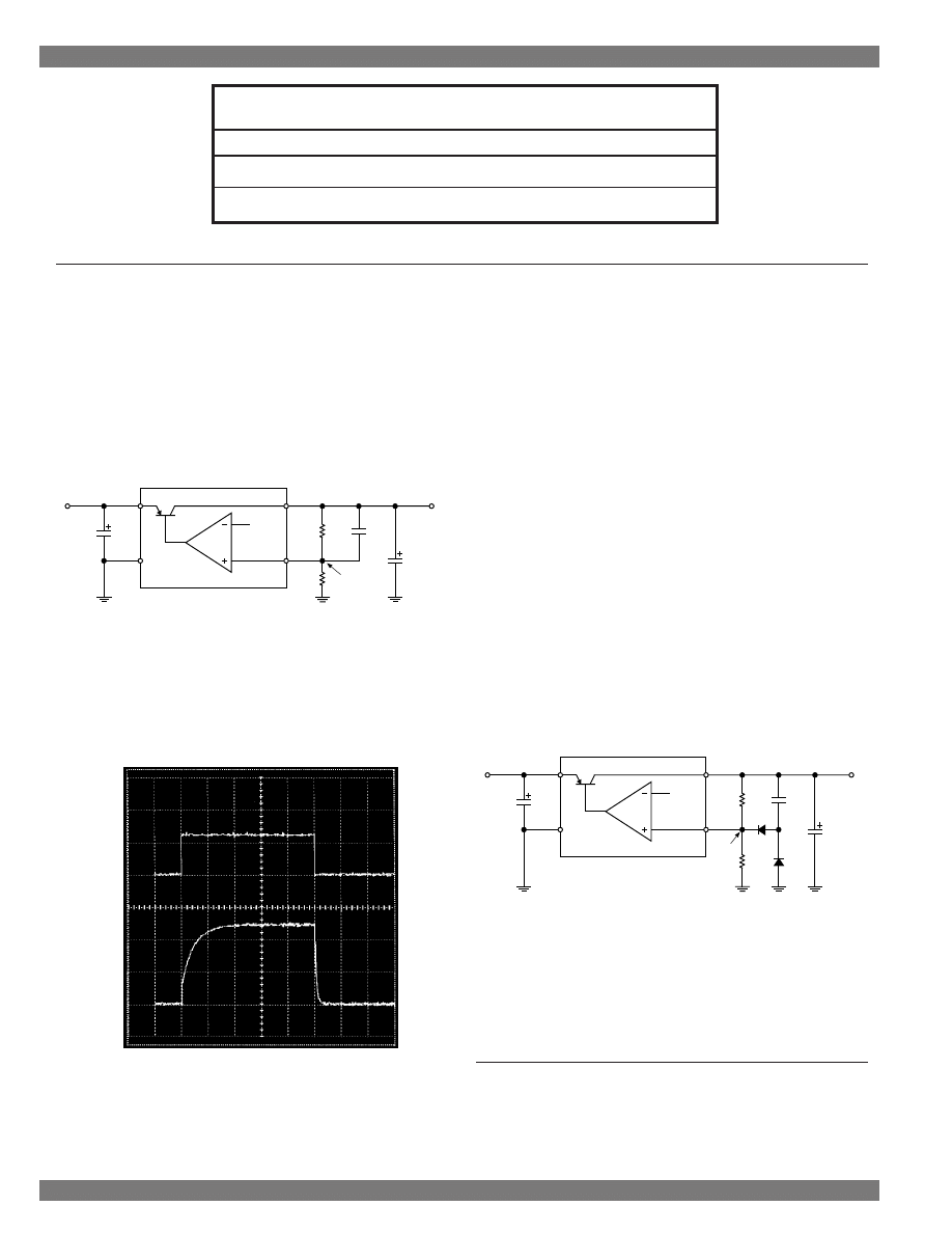
Micrel Semiconductor
Designing With LDO Regulators
Section 3: Using LDO Linear Regulators
34
Designing With Linear Regulators
The Simplest Approach
Figure 3-18 illustrates a typical LDO voltage
regulator, the MIC29152, with an additional capaci-
tor (CT) in parallel with the series leg (R1) of the feed-
back voltage divider. Since the voltage (VADJ) will
be maintained at VREF by the regulator loop, the
output of this circuit will still rapidly step to VREF (and
then rise slowly). Since VREF is usually only about
1.2V, this eliminates a large part of the surge current.
Typical LDO Regulator
V
REF
V
OUT
C
T
0.33µF
R1
300k
R2
100k
V
ADJ
OUT
IN
GND
C
IN
22µF
ADJ
MIC29152
V
IN
C
OUT
22µF
Figure 3-18. Simplest Slow Turn-On Circuit
As CT charges, the regulator output (VOUT) as-
ymptotically approaches the desired value. If a turn-
on time of 300 milliseconds is desired then about three
time constants should be allowed for charge time:
3t = 0.3s, or t = 0.1s = R1
×
CT = 300k
Ω
×
0.33
µ
F.
0
0
2
0.2
4
0.4
0.6
0.8
10
5
1.0
0
OUTPUT VOLTAGE (V) INPUT VOLTAGE (V)
TIME (s)
Figure 3-19. Turn-On Behavior for
Circuit of Figure 3-18
Figure 3-19 shows the waveforms of the circuit
of Figure 3-18. This circuit has three shortcomings:
(1) the approximately 1.2V step at turn-on, (2) the
addition of capacitor CT places a zero in the closed-
loop transfer function (which affects frequency and
transient responses and can potentially cause stabil-
ity problems) and (3) the recovery time associated
with a momentarily short-circuited output may be un-
acceptably long3.
Improving the Simple Approach
Figure 3-20 addresses the problems of poten-
tial instability and recovery time. Diode D1 is added
to the circuit to decouple the (charged) capacitor from
the feedback network, thereby eliminating the effect
of CT on the closed-loop transfer function. Because
of the non-linear effect of D1 being in series with CT,
there is a slightly longer “tail” associated with ap-
proaching the final output voltage at turn-on. In the
event of a momentarily shorted output, diode D2 pro-
vides a low-impedance discharge path for CT and
thus assures the desired turn-on behavior.
Typical LDO Regulator
V
REF
V
OUT
C
T
0.33µF
R1
300k
R2
100k
V
ADJ
OUT
IN
GND
C
IN
22µF
ADJ
MIC29152
V
IN
C
OUT
22µF
D1, D2 = 1N4148
D2
D1
Figure 3-20. Improved Slow Turn-On Circuit
Figure 3-21 shows the waveforms of the circuit
of Figure 3-20. Note that the initial step-function out-
put is now 0.6V higher than with the circuit of Figure
3-18. This (approximately) 1.8V turn-on pedestal may
Circuit
Stability
Start-Up VIN Interrupt VOUT Short
Figure
Impacted?
Pedestal?
Recovery?
Recovery?
3-18
yes
1.2V
no
no
3-20
no
1.8V
no
yes
3-22
no
0V
yes
no
NOTE 3: This is because when the output is shorted, C
T
is
discharged only by R2; if the short is removed before C
T
is fully discharged the regulator output will not exhibit the
desired turn-on behavior.
Table 3-4. Slow Turn-On Circuit Performance Features
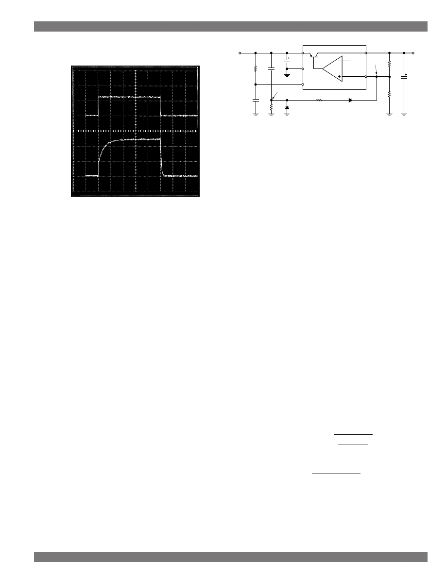
Designing With LDO Regulators
35
Section 3: Using LDO Linear Regulators
Micrel Semiconductor
Designing With LDO Regulators
be objectionable, especially in applications where the
desired final output voltage is relatively low.
0
0
2
0.2
4
0.4
0.6
0.8
10
5
1.0
0
OUTPUT VOLTAGE (V) INPUT VOLTAGE (V)
TIME (s)
Figure 3-21. Turn-On Behavior of Figure 3-20
Eliminating Initial Start-Up Pedestal
The circuits of Figures 3-18 and 3-19 depend
upon the existence of an output voltage (to create
VADJ) and, therefore, produce the initial step-func-
tion voltage pedestals of about 1.2V and 1.8V, as can
be seen in Figures 3-19 and 3-21, respectively. The
approach of Figure 3-22 facilitates placing the output
voltage origin at zero volts because VCONTROL is
derived from the input voltage. No reactive compo-
nent is added to the feedback circuit. The value of
RT should be considerably smaller than R3 to as-
sure that the junction of RT and CT acts like a volt-
age source driving R3 and so RT is the primary tim-
ing control. If sufficient current is introduced into the
loop summing junction (via R3) to generate VADJ
≥
VREF, then VOUT will be zero volts. As RT charges
CT, VCONTROL decays, which would eventually re-
sult in VADJ < VREF. In normal operation, VADJ =
VREF, so VOUT becomes greater than zero volts.
The process continues until VCONTROL decays to
VREF + 0.6V and VOUT reaches the desired value.
This circuit requires a regulator with an enable func-
tion, (such as the MIC29152) because a small (< 2V)
spike is generated coincident with application of a
step-function input voltage. Capacitor C1 and resis-
tor R4 provide a short hold-off timing function that
eliminates this spike.
Typical LDO Regulator
V
REF
V
OUT
R1
300k
R2
100k
V
ADJ
OUT
IN
GND
C
IN
22µF
ADJ
MIC29152
V
IN
C
OUT
22µF
D1
C1
0.1µF
R
T
33k
C
T
10µF
R4
240k
EN
D2
1N4001
R3
240k
V
CONTROL
1N4148
Figure 3-22. Slow Turn-On Without Pedestal
Voltage
Figure 3-23 illustrates the timing of this opera-
tion. The small initial delay (about 40 milliseconds) is
the time interval during which VADJ > VREF. Since
VIN is usually fairly consistent in value R3 may be
chosen to minimize this delay. Note that if R3 is cal-
culated based on the minimum foreseen VIN (as de-
scribed below), then higher values of VIN will pro-
duce additional delay before the turn-on ramp begins.
Conversely, if VIN(max) is used for the calculation of
R3, then lower values of VIN will not produce the de-
sired turn-on characteristic; instead, there will be a
small initial step-function prior to the desired turn-on
ramp. Recovery from a momentarily shorted output
is not addressed by this circuit, but interrupted input
voltage is handled properly. Notice that the buildup
of regulator output voltage differs from the waveforms
of Figures 3-19 and 3-21 in that it is more ramp-like
(less logarithmic). This is because only an initial por-
tion of the RC charge waveform is used; i.e., while
VCONTROL > VREF + 0.6V. The actual time con-
stant used for Figure 3-22 is 0.33 second, so 3t is
one second. As shown by Figure 3-23, this provides
about 600 milliseconds of ramp time, which corre-
sponds to the first 60% of the capacitor RC charge
curve. R3 is calculated as follows:
at turn-on time force VADJ = 1.5V
(
just slightly higher than VREF)
then
I
=
V
R1
R2
R1
R2
CONTROL
1 5
.
×
+
and
R3 =
V
0.6V
I
IN min
CONTROL
−
Since the MIC29152 is a low-dropout regulator,
6V was chosen for VIN(min). This corresponds to the
small (approximately 40msec) delay before the out-
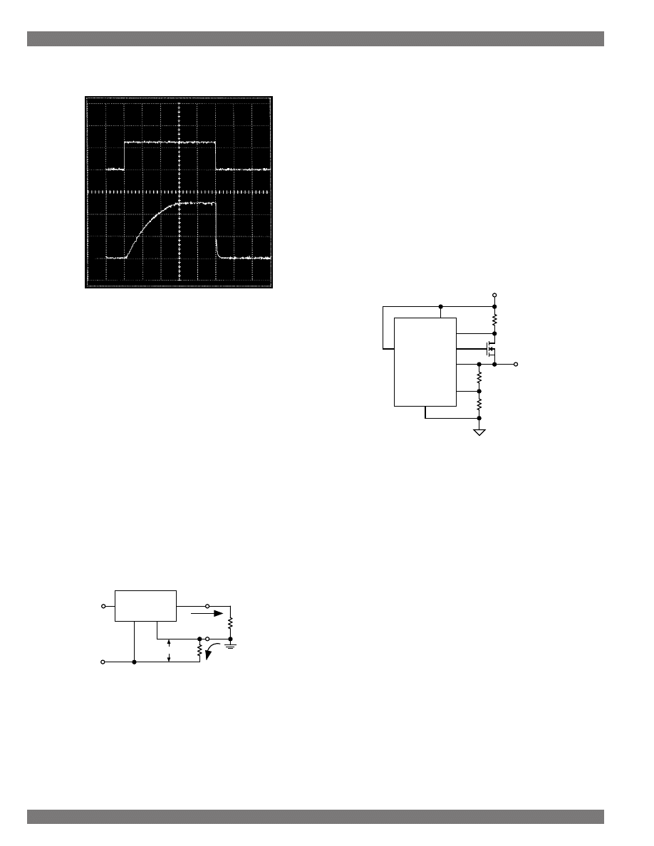
Micrel Semiconductor
Designing With LDO Regulators
Section 3: Using LDO Linear Regulators
36
Designing With Linear Regulators
put begins to rise. With 7V input the initial delay is
considerably more noticeable.
0
0
2
0.2
4
0.4
0.6
0.8
10
5
1.0
0
OUTPUT VOLTAGE (V) INPUT VOLTAGE (V)
TIME (s)
Figure 3-23. Turn-On Behavior of Figure 3-22
Current Sources
Another major application for voltage regulators
is current sources. Among other uses, most recharge-
able batteries need some type of constant current
chargers.
Simple Current Source
Several techniques for generating accurate out-
put currents exist. The simplest uses a single resis-
tor in the ground return lead (Figure 3-24). This tech-
nique works with all Micrel adjustable regulators ex-
cept for the MIC5205 or the MIC5206. The output
current is VREF
÷
R. A drawback of this simple circuit
is that power supply ground and load ground are not
common. Also, compliance ranges from 0V to only
VOUT – (VDO + VREF).
Micrel Adjustable
Regulator
1.240V
I
OUT
V
IN
ADJ
GND
R
IOUT = 1.240 / R
Load
+
–
Figure 3-24. Simple Current Source Uses
Reference Resistor in –V Return
The Super LDO Current Source
The adjustable Super LDOs, MIC5156 and
MIC5158, feature linear current limiting. This is refer-
enced to an internal 35mV source. A simple, high ef-
ficiency, high output current source may be built (Fig-
ure 3-25). Current source compliance is excellent,
ranging from zero volts to VIN – dropout, which is
only IOUT
×
RDS (ON) + 35mV (generally only a few
hundred millivolts even at 10A). Output current is
IOUT = 35mV
÷
Rs
This circuit suffers from relatively poor accuracy,
however, since the 35mV threshold is not production
trimmed. R1 and R2 allow clamping the output volt-
age to a maximum value, if desired.
GND
S
EA
MIC5158
G
EN
V
IN
R1
R2
D
Rs
V
DD
IOUT
Figure 3-25. Simple Current Source Using the
Super LDO
Accurate Current Source Using Op Amps
High accuracy and maintaining a common
ground are both possible with an alternative circuit
using two op amps and a low current MOSFET (Fig-
ure 3-26). This technique works with all Micrel ad-
justable regulators except for the MIC52xx series.
Compliance is from 0V to VIN – VDO.
A Low-Cost 12V & 5V Power Supply
Taking advantage of the low-dropout voltage
capability of Micrel’s regulators, we may build a dual
output 12V & 5V linear power supply with excellent
efficiency using a low cost 12.6V center-tapped “fila-
ment” transformer.
Figure 3-27 shows the schematic for the simple
power supply. Using a single center-tapped trans-
former and one bridge rectifier, both 12V and 5V out-
puts are available. Efficiency is high because the
transformer’s RMS output voltage is only slightly
above our desired outputs. The 12.6V center tapped
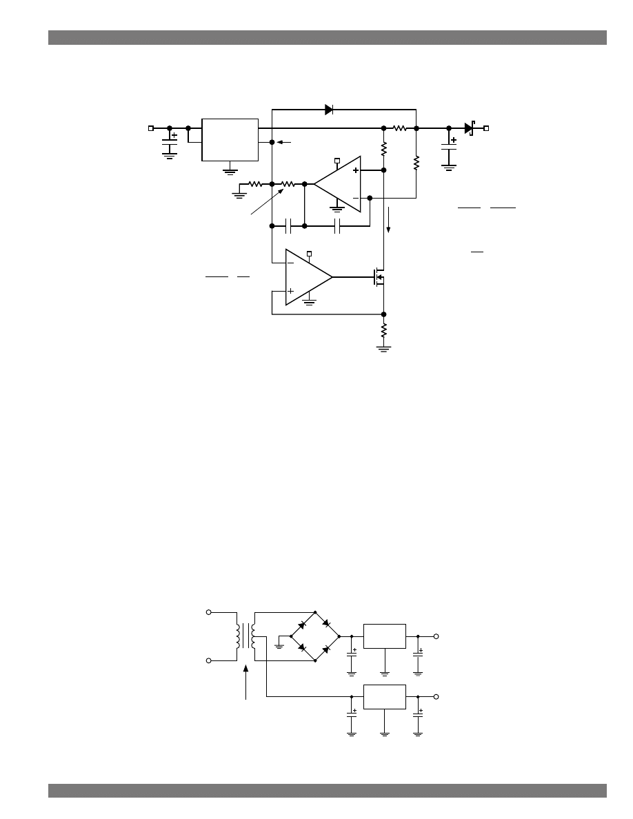
Designing With LDO Regulators
37
Section 3: Using LDO Linear Regulators
Micrel Semiconductor
Designing With LDO Regulators
IN
OUT
EN
ADJ
GND
1k
3k
R3
100k
1000pF
0.01µF
MIC6211
MIC6211
+V
IN
4
3
1
1
5
2
3
4
+V
IN
5
2
1.24V
V
2
V
2
I
1
R1
1.24k
VN2222
1N4148
10k
R2 100m
Ω
330µF
I
OUT
1A
68µF
4V to 6V
MIC29152
I
R1
R3
R2
OUT
=
×
1 240
.
I
R1
V
V
R3
1
2
=
×
−
1 240
.
I
V
R2
OUT
=
Reduce to 2k
if V
IN
< 5V
Figure 3-26. Current Source Using a Pair of Op-Amps
filament transformer is a decades-old design origi-
nally used for powering vacuum tube heaters. It is
perhaps the most common transformer made. The
outside windings feed the bridge rectifier and filter
capacitor for the 12V output. A MIC29150-12 pro-
duces the regulated 12V output. The transformer cen-
ter tap feeds the 5V filter capacitor and the MIC29150-
5.0 directly—
no rectifier diode is needed.
This circuit may be scaled to other output cur-
rents as desired. Overall efficiency is extremely high
due to the low input voltage, so heat sinking require-
ments are minimal. A final benefit: since the power
tabs of the TO-220 packages are at ground potential,
a single non-isolated, non-insulated heat sink may
be used for both regulators.
AC Input
12.6V CT
Filament
Transformer
MIC29150-12
MIC29150-5.0
12.0V
5.0V
Figure 3-27. A Dual-Output Power Supply From a Single Transformer and Bridge Rectifier

Micrel Semiconductor
Designing With LDO Regulators
Section 3: Using LDO Linear Regulators
38
Designing With Linear Regulators
jumper-selected resistors. They are fast starting, and
may optionally provide ON/OFF control and an error
flag that indicates power system trouble.
Dropout Requirements
While linear regulators are extremely easy to
use, one design factor must be considered: dropout
voltage. For example, a regulator with 2 volts of drop-
out producing a 3.3V output requires over 5.3 volts
on its input. Furthermore, reliable circuit operation
requires operating a linear regulator above its drop-
out region—in other words, with a higher than mini-
mum input voltage. In dropout, the regulator is not
regulating and it responds sluggishly to load changes.
What is the required dropout voltage perfor-
mance? Let’s assume we have a 5V supply and need
to provide 3.525V to our microprocessor. The worst
case occurs when the input voltage from the 5V sup-
ply is at its minimum and the output is at its maxi-
mum. An example will illustrate.
VIN =
5V – 5% =
4.75V
VOUT = 3.525V + 2% = 3.60V
Maximum Allowable
Dropout Voltage:
1.15V
This simplified example does not include the ef-
fects of power supply connector, microprocessor
socket, or PC board trace resistances, which would
further subtract from the required dropout voltage.
Fast response to load current changes (from a pro-
cessor recovering from “sleep” mode, for example)
occurs only when the regulator is away from its drop-
out point. In real systems, a maximum dropout volt-
age between 0.6V to 1V is ideal. Achieving this per-
formance means the output device must be either a
PNP bipolar transistor or a MOSFET.
Historically, linear regulators with PNP outputs
have been expensive and limited to low current ap-
plications. However, Super ßeta PNP low dropout
regulators provide up to 7.5 amperes of current with
dropout voltages less than 0.6V, guaranteed. A lower
cost product line outputs the same currents with only
1V of dropout. These low dropout voltages guaran-
tee the microprocessor gets a clean, well regulated
supply that quickly reacts to processor-induced load
changes as well as input supply variations.
The low dropout linear voltage regulator is an
easy-to-use, low cost, yet high performance means
Computer Power Supplies
The decreasing silicon geometries of micropro-
cessors and memory have forced a reduction in op-
erating voltage from the longtime standard of 5V. This
rise of sub-5V microprocessors, logic, and memory
components in personal computer systems created
demand for lower voltage power supplies. Several
options exist for the desktop computer system de-
signer. One of these options is to provide both 3.3V
and 5.0V from the main system power supply. An-
other is to use the existing high current 5V supply
and employ a low dropout (LDO) linear regulator to
provide 3.3V.
The low-cost, production proven desktop com-
puter power supplies output
±
5V and
±
12V—but not
3V. Redesigning the system power supply would in-
crease cost and break the long standing power sup-
ply to motherboard connector standard which has no
provision for 3V. Further complicating matters is that
“3V” is not really defined. Microprocessor manufac-
turers produce devices requiring 2.9V, 3.3V, 3.38V,
3.45V, 3.525V, 3.6V, and several other similar volt-
ages. No single standard has been adopted. Design-
ing and stocking dedicated power supplies for all of
these different voltages would be extremely difficult
and expensive. Also, motherboard makers want to
maximize their available market by allowing as many
different microprocessors as possible on each board;
this means they must design an on-board supply that
produces all of the most popular voltages to remain
competitive. This is even more important for the moth-
erboard vendors who sell boards sans-microproces-
sor. They must not only provide the expected volt-
ages, they must simplify the selection process so that
all system integrators—and even some end users—
may configure the voltage properly. With too low an
operating voltage, the microprocessor will generate
errors; too high a voltage is fatal.
Instead, system integrators use motherboards
with an on-board power supply, which converts the
readily available +5V source into the required low
voltage output. The simplest, lowest cost solution for
this problem is the modern, very low dropout version
of the venerable linear regulator. This is a low cost
option, requiring only quick design work and little
motherboard space. Linear regulators provide clean,
accurate output and do not radiate RFI, so govern-
ment certification is not jeopardized. Adjustable lin-
ear regulators allow voltage selection by means of
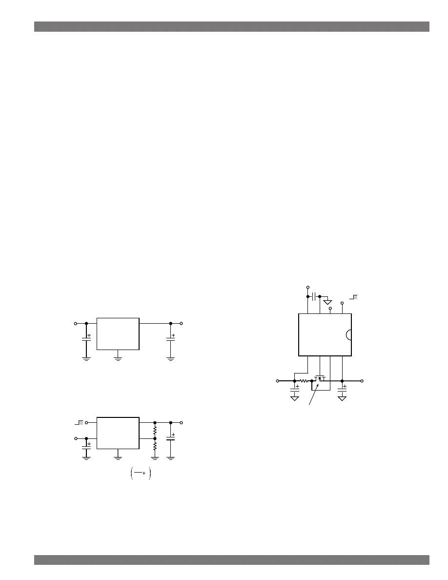
Designing With LDO Regulators
39
Section 3: Using LDO Linear Regulators
Micrel Semiconductor
Designing With LDO Regulators
of powering high performance low voltage micropro-
cessors. By selecting a modern low dropout regula-
tor, you assure reliable operation under all working
conditions.
5V to 3.xV Conversion Circuits
Recommended circuits for on-board desktop
computer power supplies follow. Due to the high
speed load changes common to microprocessors, fast
load transient response is crucial. This means circuit
layout and bypass and filter capacitor selection is also
critical. At low current levels, thermal considerations
are not difficult; however, at currents of above 3 am-
peres, the resulting heat may be troublesome.
Method 1: Use a Monolithic LDO
The simplest method of providing a second VCC
on a computer motherboard is by using a monolithic
regulator. If the required voltage is a standard value,
a fixed-voltage regulator is available. In this ideal situ-
ation, your electrical design consists of merely speci-
fying a suitable output filter capacitor. If the output
voltage is not available from a fixed regulator,
adjustables are used. They use two resistors to pro-
gram the output voltage but are otherwise similar to
the fixed versions. Figure 3-28 and 3-29 show fixed
and adjustable regulator applications.
MIC29710
OUT
V
OUT
IN
GND
V
IN
Figure 3-28. Fixed Regulator Circuit Suitable for
Computer Power Supply Applications
MIC29712
OUT
ADJ
R1
V
OUT
R2
EN
GND
V
IN
IN
On
Off
V
OUT
= 1.240
R1
R2
1
Figure 3-29. Adjustable Regulator Circuit Suitable
for Computer Power Supply Applications
Method 2: The MIC5156 “Super LDO”
The Micrel MIC5156 is a linear regulator con-
troller that works with a low cost N-Channel power
MOSFET to produce a very low dropout regulator
system. The MIC5156 is available in a small 8-pin
SOIC or in a standard 8-pin DIP, and offers fixed 3.3V,
5.0V, or user selectable (adjustable) voltage outputs.
Figure 2 shows the entire schematic—two filter ca-
pacitors, a MOSFET, and a printed circuit board trace
about a centimeter long (used as a current sense
resistor) is all you need for the fixed voltage version.
For the adjustable part, add two resistors. The
MIC5156 requires an additional power supply to pro-
vide gate drive for the MOSFET: use your PC’s 12V
supply—the current drawn from the 12V supply is very
small; approximately one milliampere. If a 12V sup-
ply is not available, the MIC5158 generates its own
bias and does not need an additional supply.
Figure 3-30 shows a typical 3.3V and 5V com-
puter power supply application. The MIC5156 pro-
vides regulated 3.3V using Q1 as the pass element
and also controls a MOSFET switch for the 5V sup-
ply.
1
2
3
8
7
6
4
5
MIC5156-3.3
V
P
GND
FLAG
EN
V
DD
G
D
S
V
OUT
3.3V, 10A
V
IN
5V
0.1µF
R
S
R
S
= 0.035V / I
LIMIT
3m
Ω
SMP60N03-10L
C
L
*
47µF
* Improves transient
response to load changes
+12V
Enable
Shutdown
47µF
Figure 3-30. MIC5156 5V-to-3.3V Converter
When the 3.3V output has reached regulation,
the FLAG output goes high, enhancing Q2, which
switches 5V to Load 2. This circuit complies with the
requirements of some dual-voltage microprocessors
that require the 5V supply input to remain below 3.0V
until the 3.3V supply input is greater than 3.0V.
An optional current limiting sense resistor (RS)
limits the load current to 12A maximum. For less costly
designs, the sense resistor’s value and function can
be duplicated using one of two techniques: A solid
piece of copper wire with appropriate length and di-
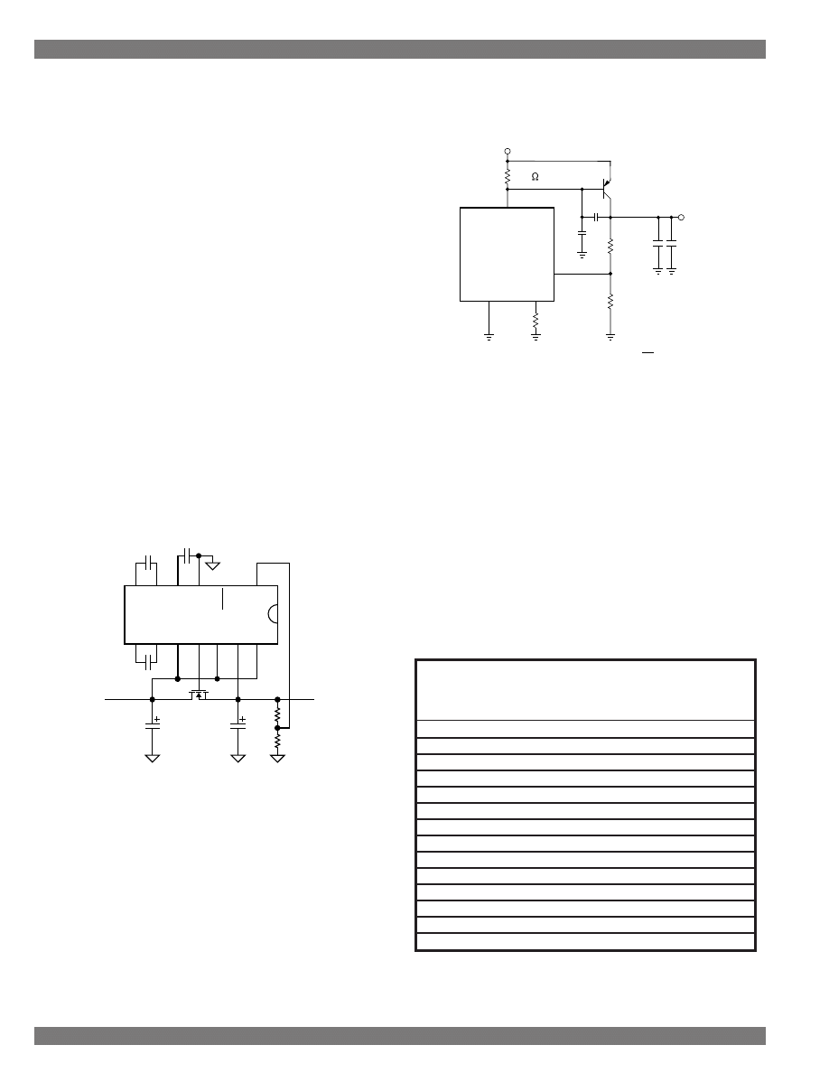
Micrel Semiconductor
Designing With LDO Regulators
Section 3: Using LDO Linear Regulators
40
Designing With Linear Regulators
ameter (gauge) makes a reasonably accurate low-
value resistor. Another method uses a printed circuit
trace to create the sense resistor. The resistance
value is a function of the trace thickness, width, and
length. See
Alternative Resistors, in Section 4, for
current sense resistor details.
NOTE: the tab of the power MOSFET is con-
nected to +5V. Use an insulator between the MOS-
FET and the heat sink, if necessary.
Method 3: The MIC5158 “Super LDO”
Like the MIC5156, the MIC5158 is a linear regu-
lator controller that works with a low cost N-Channel
power MOSFET to produce a very low dropout regu-
lator system. The MIC5158, however, generates the
bias voltage required to drive the N-channel MOS-
FET and does not require a 12V supply. Its on-board
charge pump uses three capacitors and takes care
of the level shifting. Figure 3-31 shows the MIC5158
circuit.
An idea for the motherboard manufacturer: build
the MIC5158 circuit on a plug-in daughterboard with
three or five pins that allow it to mount on the system
board like a monolithic regulator.
1
2
3
4
14
13
12
11
5
6
7
10
9
8
MIC5158
C1+
C1–
V
DD
V
OUT
3.3V, 10A
V
IN
(5V)
C2
0.1µF
C3
3.3µF
C1
0.1µF
C
OUT
47µF
* For V
IN
> 5V, use IRFZ44.
C2+
C2–
GND
G
D
S
V
CP
FLAG
R1
17.8k
Ω
, 1%
R2
10.7k
Ω
, 1%
Q1*
IRLZ44
C
IN
47µF
EN
5V FB
EA
Figure 3-31. MIC5158 5V-to-3.3V Converter
Method 4: Current Boost a MIC2951
The 150mA MIC2951 gets a capacity boost to
several amperes by using an external PNP transis-
tor. Figure 3-32 shows the MIC2951 driving a DH45H8
or equivalent PNP transistor to achieve a 3A output.
This circuit has a number of problems, including poor
stability (a large output capacitor is required to squelch
oscillations), poor current limiting characteristics, poor
load transient response, no overtemperature shut-
down protection, and requires numerous external
components. It is not recommended.
LP2951
GND
4
7
8
VOUT
+VIN
Feedback
PNP Pass Element
(TIP127 or D45H8)
R1
R2
+
0.1µF
1
39
Ω
+VOUT
(3.3V to 3.83V
@ 0.1 to 3A
680µF
VOUT = 1.235V (1+ )
R1
R2
+4.75 to 5.25V
390
0.1µF
0.1µF
R1 = 158k
Ω
R2 = 75k to 95.3k
Ω
Figure 3-32. PNP Transistor Boosts Current Output
From MIC2951 Regulator
Adjust Resistor Values
Table 3-5 shows recommended resistor values
for various voltages. The values shown represent the
calculated closest-match for the desired voltage us-
ing standard 1% tolerance resistors. Since Micrel’s
adjustable regulators use a high impedance feedback
stage, large value adjust resistors are generally rec-
ommended. Valid resistor values range from a few
ohms to about 500k
Ω
.
While the MIC29152/29302/29502 have a
1.240V reference, the Super LDO and current boosted
MIC2951 circuits use a 1.235V reference.
Figs. 3-28 & 29
Figs. 3-30, 31, & 32
(V
REF
= 1.240V)
(V
REF
= 1.235V)
Voltage
R1
R2
R1
R2
1.5
80.6k 16.9k
53.6k 11.5k
1.8
237k
107k
301k
137k
2.85
287k
221k
187k
143k
2.9
162k
121k
137k
102k
3.0
102k
71.5k
150k
105k
3.1
158k
105k
154k
102k
3.15
191k
124k
158k
102k
3.3
196k
118k
178k
107k
3.45
221k
124k
191k
107k
3.6
102k
53.6k
383k
200k
3.8
221k
107k
221k
107k
4.0
255k
115k
115k
51.1k
4.1
316k
137k
232k
100k
4.5
137k
52.3k
107k
40.2k
Table 3-5. Suggested Adjust Resistor Values
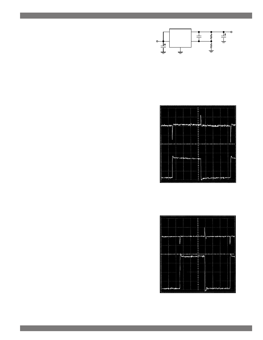
Designing With LDO Regulators
41
Section 3: Using LDO Linear Regulators
Micrel Semiconductor
Designing With LDO Regulators
3.3V to 2.xV Conversion
Like the 5V to 3.3V conversion discussed above,
dropping to voltages below 3.3V from a 3.3V rail is a
useful application for LDO regulators. Here, the regu-
lator dropout voltage is much more critical. Applica-
tions using 2.9V only have 400mV of headroom when
powered from a perfect 3.3V supply. For the stan-
dard 3.3V supply tolerance of
±
300mV, the headroom
drops to only 100mV. For this situation, the most rea-
sonable solution is one of the Super LDO circuits
shown in Figures 3-30 and 3-31. These circuits fea-
ture excellent efficiency—approximately 88%. Mono-
lithic LDO solutions powered from a standard 3.3V
±
300mV supply become tenable with output voltages
of 2.5V or below.
Improving Transient Response
Modern low-voltage microprocessors have mul-
tiple operating modes to maximize both performance
and minimize power consumption. They switch be-
tween these modes quickly, however, which places a
strain on their power supply. Supply current varia-
tions of several orders of magnitude in tens of nano-
seconds are standard for some processors—and they
still require that their supply voltage remain within
specification throughout these transitions.
Micrel low-dropout regulators have excellent re-
sponse to variations in input voltage and load cur-
rent. By virtue of their low dropout voltage, these de-
vices do not saturate into dropout as readily as simi-
lar NPN-based designs. A 3.3V output Super
β
eta
PNP LDO will maintain full speed and performance
with an input supply as low as 4.2V, and will still pro-
vide some regulation with supplies down to 3.8V,
unlike NPN devices that require 5.1V or more for good
performance and become nothing more than a resis-
tor under 4.6V of input. Micrel’s PNP regulators pro-
vide superior performance in “5V to 3.3V” conversion
applications, especially when all tolerances are con-
sidered.
Figure 3-33 is a test schematic using the Intel®
Pentium™ Validator. The Validator is a dynamic load
which simulates a Pentium processor changing states
at high speed. Using Figure 3-33, the MIC29512 (Fig-
ure 3-34) was tested with fast 200mA to 5A load tran-
sitions. The MIC29712 was tested with fast transi-
tions between 200mA and 7.5A (Figure 3-35).
V
IN
= V
OUT
+ 1V
MIC29712
EN
IN
OUT
ADJ
GND
0.1µF
93.1k
1%
49.9k
1%
V
OUT
3.525V nominal
6
×
330µF
AVX
TPSE337M006R0100
tantalum
V
OUT
load (not shown):
Intel® Power Validator
Figure 3-33. Load Transient Response Test Circuit.
Super LDO System Driving an Intel Pentium
“Validator” Test System
0mA
200mA
5A
3.525V
+20mV
–20mV
LOAD CURRENT OUTPUT VOLTAGE
MIC29512 Load Transient Response
(See Test Circuit Schematic)
1ms/division
Figure 3-34. MIC29512 Load Transient Response
0A
3.525V
+50mV
–50mV
LOAD CURRENT OUTPUT VOLTAGE
MIC29712 Load Transient Response
(See Test Circuit Schematic)
1ms/division
2A
200mA
4A
6A
8A
Figure 3-35. MIC29712 Load Transient Response.
Load Varies from 200mA to 7.5A
Micrel Semiconductor
Designing With LDO Regulators
Section 3: Using LDO Linear Regulators
42
Designing With Linear Regulators
The following photographs show the transient
response of the MIC5156 Super LDO with an IRL3103
power MOSFET (RDS (ON)
≤
14m
Ω
, Ciss = 1600pF)
driving the Intel Pentium™ Validator. Figure 3-36
shows the performance with four (4) 330
µ
F AVX sur-
face mount capacitors. The peak transient response
voltage is –55mV on attack and +60mV on turn-off.
Figure 3-37 shows the tremendous improvement an-
other four 330
µ
F capacitors make: with eight (8)
330
µ
F AVX capacitors, the transient peaks drop to
only approximately
±
25mV. These measurements are
made with VDD = 5.0V, VP = 12.0V, and a single
330
µ
F bypass capacitor on the VDD input to the
MIC5156. As both the 5156 and the MIC5158 use
the same error amplifier circuit, their transient re-
sponse should be similar. Furthermore, the transient
response of the MIC5156 does not change as the
input voltage (VDD) decreases from 5.0V down to
nearly dropout levels (a bit less than 3.6V input with
the 3.525V output).
Accuracy Requirements
Microprocessors have various voltage tolerance
requirements. Some are happy with supplies that
swing a full
±
10%, while others need better than
±
2.5% accuracy for proper operation. Fixed 3.3V de-
vices operate well with any of these microprocessors,
since Micrel guarantees better than
±
2% across the
operating load current and temperature ranges. Lo-
cating the regulator close to the processor to mini-
mize lead resistance and inductance is the only de-
sign consideration that is necessary. Microprocessors
that use nonstandard or varying voltages have a prob-
lem: while the basic adjustable regulator offers
±
1%
accuracy and
±
2% worst case over temperature ex-
tremes, any error in the external programming resis-
tors (either in tolerance or compromise in resistance
ratio that is unavoidable when using standardized
resistor values) directly appears as output voltage
error. The error budget quickly disappears. See
Ad-
justable Regulator Accuracy Analysis, in this section,
for a discussion of voltage tolerance and sensitivity.
When any trace resistance effects are consid-
ered, it is painfully apparent that this solution will not
provide the needed
±
2.5% accuracy. Resistors of
0.1% tolerance are one step. Other ideas are pre-
sented in
Improving Regulator Accuracy, also in this
section.
Figure 3-36. Transient response of the MIC5156
Super LDO driving an Intel Pentium “Validator”
microprocessor simulator. Output capacitance is 4
×
330
µ
F.
Figure 3-37. Transient response of the MIC5156
Super LDO driving an Intel Pentium “Validator”
microprocessor simulator. Output capacitance is 8
×
330
µ
F.
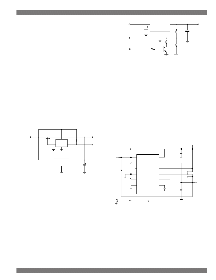
Designing With LDO Regulators
43
Section 3: Using LDO Linear Regulators
Micrel Semiconductor
Designing With LDO Regulators
Multiple Output Voltages
Another design parameter computer mother-
board designers cope with is the need to support dif-
ferent types of microprocessors with one layout. Since
processors in a single family may require different
voltages, it is no surprise that different processor types
also may need various supply voltages. Since it is
expensive to provide multiple variable outputs from
the system power supply, the economical solution to
this problem is to generate or switch between sup-
plies directly on the motherboard.
Occasionally, a designer will get lucky and some
motherboard options can use a standard voltage from
the power supply. In this case, we may switch the
higher voltage around the LDO generating the lower
voltage, as shown in Figure 3-38. This circuit was
designed to allow Intel DX4Processors™, running on
3.3V, to operate in the same socket as a standard 5V
486. A pin on the DX4Processor is hard wired to
ground, which provides the switching needed for au-
tomatically selecting the supply voltage. Standard 486
processors have no connection to this pin.
MIC29300-3.3
47µF
MIC5014
N-channel MOSFET
RON
≤
80m
Ω
100k
Ω
VCC IN
(5v
±
5%)
VCC OUT at 3A
V+
Input
Source
Gnd
Gate
Input
Gnd
Output
High or Open = 5V
Low = 3.3V
Voltage Selection Input
Figure 3-38. Switching 5V or 3.3V
to a Microprocessor
This circuit capitalizes on the reversed-battery
protection feature built into Micrel’s Super
β
eta PNP
regulators. The regulators survive a voltage forced
on their output that is higher than their programmed
output. In this situation, the regulator places its pass
transistor in a high impedance state. Only a few mi-
croamperes of current leaks back into the regulator
under these conditions, which should be negligible.
Note that an adjustable regulator could be used in
place of the fixed voltage version shown.
An adjustable regulator and an analog switch
will perform this task, as shown in Figure 3-39. Only
one supply (of the maximum desired output voltage,
or higher) is necessary.
MIC29302
47µF
VCC IN
(5V
±
5%)
VCC OUT
Input
Gnd
Output
Voltage Selection Input
High = 5V
Low or Open = 3.3V
ENABLE
Adj
4.7µF
ON/OFF
(Optional)
300k
Ω
180k
Ω
220k
Ω
330k
Ω
2N2222 or equiv.
(3A)
Figure 3-39. Adjustable LDO and analog switch
provides selectable output voltages
Another method of providing two or more output
voltages to a socket with the higher of the two pro-
vided is by using the Super LDO. Program the ad-
justable MIC5156 or MIC5158 as shown in Figure 3-
40. When the higher of the two voltages is chosen,
the regulator simply acts as a low-loss switch. Use a
transistor switch to select the lower voltage. This tech-
nique may be expanded to any number of discrete
voltages, if desired. The MIC5158 will operate from a
single input supply of 3.0V or greater. The MIC5156
needs a low current 12V supply to provide gate bias
for the pass MOSFET, but if this is available, it is
smaller than the MIC5158 and requires no charge
pump capacitors.
10µF
0.1µF
47µF
VIN (+5V)
VOUT
10k
Ω
0.1µF
1µF
n.c.
MIC5158
"Super LDO"
7
6
5
4
3
2
1
8
9
10
11
12
13
14
G
D
S
ENABLE
n.c.
16.9k
Ω
12.1k
Ω
2N2222 or equivalent
330k
Ω
Low (or open) = 3.3V
High = 5V
Figure 3-40. MIC5158 with Selectable
Output Voltages
Figure 3-41 is a switched voltage PNP regulator
that relies on jumpers for output voltage programming.
While perhaps not as “elegant” as the previous tech-
niques, it provides full functionality and flexibility. This
circuit was designed so if all jumpers are accidentally
removed, the output voltage drops to its lowest value.
By configuring the jumpers as shown, the system is
relatively safe—if someone inadvertently removes all
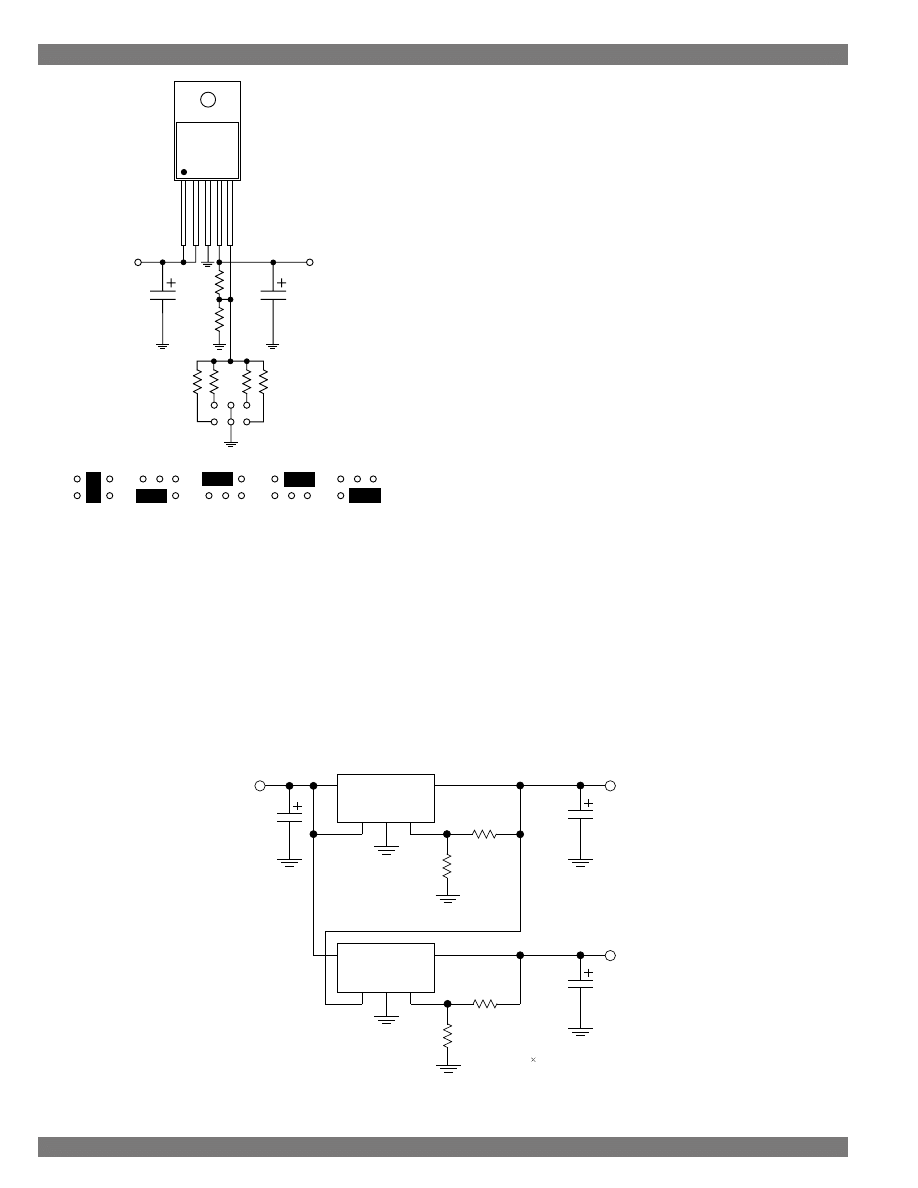
Micrel Semiconductor
Designing With LDO Regulators
Section 3: Using LDO Linear Regulators
44
Designing With Linear Regulators
MIC29712
MIC29512
220µF
47µF
4V to 6V
Supply 1
3.3V at 7.5A
R1 205k
Ω
R2
124k
Ω
VOUT = 1.240 (1 + R1/R2)
VIN
VOUT
EN
ADJ
GND
VIN
VOUT
EN
ADJ
GND
220µF
Supply 2
2.5V at 5A
(Sequenced
After Supply 1)
R1 127k
Ω
R2
124k
Ω
Figure 3-42. Multiple Supply Sequencing
3.45
3.30
3.38
3.45V
3.30
3.38
3.53V
2.90V
3.30
3.38
237
Ω
VIN
4.75V to 5.25V
VOUT to Microprocessor
2.90V to 3.53V
MIC29302BT
10µF
2.2µF
3.38
3.30
3.45
3.53
475
Ω
549
Ω
634
Ω
750
Ω
3.38
3.38V
3.30V
Voltage Jumper Positions
176
Ω
Figure 3-41. Jumper Selectable Output Voltages
Multiple Supply Sequencing
Some microprocessors use multiple supply volt-
ages; a voltage for the core, another for the cache
memory, and a different one for I/O, for example. Se-
quencing these supplies may be critical to prevent
latch-up. Figure 3-42 shows an easy way of guaran-
teeing this sequencing using Micrel’s regulators with
an enable control. As the output voltage of Supply 1
rises above 2V, the regulator for Supply 2 starts up.
Supply 2 will never be high until Supply 1 is active.
Supply 1 need not be the higher output voltage; it
must only be 2.4V or above (necessary to assure the
second regulator is fully enabled). Note that Supply 1
may not need an enable pin.
This technique works with the MIC29151 through
MIC29752 monolithic regulators as well as with the
Super LDO (MIC5156/57/58). It also is applicable for
systems requiring any number of sequenced supplies,
although for simplicity we only show two supplies
here.
Thermal Design
Once the electrical design of your power sys-
tem is complete, we must deal with thermal issues.
While they are not terribly difficult, thermal design is
lightly covered in most electrical engineering curricu-
lum. Properly addressing thermal issues is impera-
tive to LDO system reliability, and is covered in detail
in
Thermal Management, later in this section.
the jumpers, the output voltage drops to a low value.
While the system may be error-prone or nonfunctional
with this low voltage, at least the microprocessor will
survive.
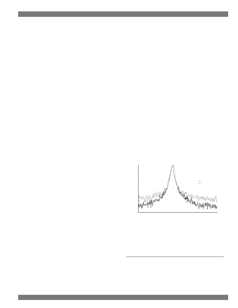
Designing With LDO Regulators
45
Section 3: Using LDO Linear Regulators
Micrel Semiconductor
Designing With LDO Regulators
Portable Devices
Voltage regulators are necessary in almost all
electronic equipment, and portable devices are no
exception. Portable equipment includes cellular and
“wireless” telephones, radio receivers and handheld
transceivers, calculators, pagers, notebook comput-
ers, test equipment, medical appliances and most
other battery operated gear.
Design Considerations
Portable electronics are characterized by two
major distinguishing features:
• Small size
• Self-contained power source (batteries)
Beyond these similarities, portable equipment
power requirements vary as much as their intended
application.
Small Package Needed
Portable devices are, by definition, relatively
small and lightweight. Most circuitry is surface
mounted and power dissipation is normally minimized.
Self Contained Power
Most portable equipment is battery powered.
Batteries are often the largest and heaviest compo-
nent in the system, and may account for 80% or more
of the total volume and mass of the portable device.
Power conservation is an important design consider-
ation. Low power components are used and power
management techniques, such as “sleep mode”, help
maximize battery life. Just as one is never too rich,
one’s batteries never last long enough!
Yet another battery-imposed limitation is that
batteries are available in discrete voltages, deter-
mined by their chemical composition. Converting
these voltages into a constant supply suitable for elec-
tronics is the regulator’s most important task.
Low Current (And Low Voltage)
The regulators used in portable equipment are
usually low output current devices, generally under
250mA, since their loads are also (usually) low cur-
rent. Few portable devices have high voltage loads4
and those that do need little current.
Low Output Noise Requirement
Cellular telephones, pagers, and other radios
have frequency synthesizers, preamplifiers, and mix-
ers that are susceptible to power supply noise. The
frequency synthesizer voltage controlled oscillator
(VCO), the block that determines operating frequency,
may produce a noisy sine wave output (a wider band-
width signal) if noise is present on VCC. Making mat-
ters worse for portable equipment designers, lower
powered/lower cost VCOs are generally more sus-
ceptible to VCC noise.
Ideal VCOs produce a single spectral line at the
operating frequency. Real oscillators have sideband
skirts; poor devices have broad skirts. Figure 3-43
shows the measured phase noise from a free run-
ning Murata MQE001-953 VCO powered by a
MIC5205 low-noise regulator. Note the significant
improvement when using the noise bypass capaci-
tor. Regulators not optimized for noise performance
produce skirts similar to or worse than the MIC5205
without bypass capacitors.
Broad oscillator skirts decrease the noise figure
and the strong signal rejection capability of receivers
(reducing performance) and broaden the transmitted
signal in transmitters (possibly in violation of spectral
purity regulations).
-80
-70
-60
-50
-40
-30
-20
-10
0
-23.75
-21.75
-19.75
-17.75
-15.75
-13.75
-11.75
-9.75
-7.75
-5.75
-3.75
-1.75
0.25
2.25
4.25
6.25
8.25
10.25
12.25
14.25
16.25
18.25
20.25
22.25
24.25
Frequency Offset from Carrier (kHz)
dBc
No Capacitor
47pF Bypass Cap
Figure 3-43. A Low-Noise LDO (MIC5205) Reduces
VCO Phase Noise
Although not as susceptible to noise as VCOs,
preamplifiers and mixers operating from noisy sup-
plies also reduce receiver and transmitter perfor-
mance in similar ways.
NOTE 4: The notable exceptions to this statement are the
fluorescent backlights in notebook computers and the
electroluminescent lamps in telephones, watches, etc.
These lamps must be driven with a switching regulator
that boosts the battery voltage—something a linear
regulator cannot do.
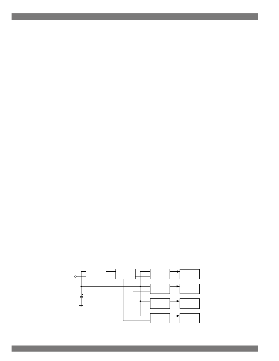
Micrel Semiconductor
Designing With LDO Regulators
Section 3: Using LDO Linear Regulators
46
Designing With Linear Regulators
Dropout and Battery Life
Low dropout regulators allow more operating life-
time from batteries by generating usable output to
the load well after standard regulators would be satu-
rated. This allows discharging batteries to lower lev-
els or—in many cases—eliminating a cell or two from
a series string. Compared to older style regulators
with 2 to 3V of dropout, Micrel’s 0.3V to 0.6V LDOs
allow eliminating one to two alkaline, NiCd, or NiMH
cells.
Ground Current and Battery Life
The quiescent, or ground, current of regulators
employed inside portable equipment is also impor-
tant. This current is yet another load for the battery,
and should be minimized.
Battery Stretching Techniques
Sleep Mode Switching
Sleep mode switching is an important technique
for battery powered devices. Basically, sleep mode
switching powers down system blocks not immedi-
ately required. For example, while a cellular phone
must monitor for an incoming call, its transmitter is
not needed and should draw no power; it can be shut
off. Likewise, audio circuits may be powered down.
Portable computers use sleep mode switching by
spinning down the hard disk drive and powering down
the video display backlight, for example. Simpler de-
vices like calculators automatically turn off after a
certain period of inactivity.
Micrel’s LDO regulators make sleep mode imple-
mentation easy because each family has a version
with logic-compatible shutdown control. Many fami-
lies feature “zero power” shutdown—when disabled,
the regulator fully powers down and draws virtually
zero current.5 Designers updating older systems that
used MOSFETs for switching power to regulators may
now eliminate the MOSFET. The regulator serves as
switch, voltage regulator, current limiter, and overtem-
perature protector. All are important features in any
type of portable equipment.
Power Sequencing
A technique related to Sleep Mode Switching is
Power Sequencing. This is a power control technique
that enables power blocks for a short while and then
disables them. For example, in a cellular telephone
awaiting a call, the receiver power may be pulsed on
and off at a low-to-medium duty cycle. It listens for a
few milliseconds each few hundred milliseconds.
Multiple Regulators Provide Isolation
The close proximity between different circuit
blocks naturally required by portable equipment in-
creases the possibility of interstage coupling and in-
terference. Digital noise from the microprocessor may
interfere with a sensitive VCO or a receiver preampli-
fier, for example. A common path for this noise is the
common supply bus. Linear regulators help this situ-
ation by providing active isolation between load and
input supply. Noise from a load that appears on the
regulator’s output is greatly attenuated on the
regulator’s input.
Figure 3-44 shows a simplified block diagram of
a cellular telephone power distribution system. Be-
tween five and seven regulators are used in a typical
telephone, providing regulation, ON/OFF (sleep
mode) switching, and active isolation between stages.
IN
CTL
OUT
Power
Switch
Microcontroller
IN
CTL
OUT
IN
CTL
OUT
IN
CTL
OUT
IN
CTL
OUT
MIC5207
MIC5205
MIC5203
MIC5203
MIC5203
VCO
Power Amp
RF/IF Stages
Audio, etc.
Figure 3-44. Cellular Telephone Block Diagram
NOTE 5: In the real world, there is no such thing as zero, but
Micrel’s regulators pass only nanoamperes of device
leakage current when disabled—“virtually zero” current.
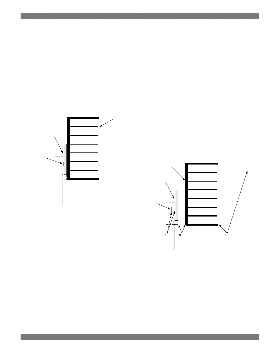
Designing With LDO Regulators
47
Section 3: Using LDO Linear Regulators
Micrel Semiconductor
Designing With LDO Regulators
Thermal Management
A Thermal Primer
Micrel low dropout (LDO) regulators are very
easy to use. Only one external filter capacitor is nec-
essary for operation, so the electrical design effort is
minimal. In many cases, thermal design is also quite
simple, aided by the low dropout characteristic of
Micrel’s LDOs. Unlike other linear regulators, Micrel’s
LDOs operate with dropout voltages of 300mV–often
less. The resulting Voltage
×
Current power loss can
be quite small even with moderate output current. At
higher currents and/or higher input-to-output voltage
differentials, however, selecting the correct heat sink
is an essential “chore”.
Die
(junction)
Package
(case)
Heat Sink
Figure 3-45. Regulator Mounted to a Heat Sink
Thermal Parameters
Before working with thermal parameters, we will
define the applicable symbols and terms.
∆
T
Temperature rise (temperature
difference,
°
C)
q
Heat flow (Watts)
θ
Thermal resistance (
°
C/W)
PD
Power Dissipation (Watts)
θ
JA
Thermal resistance, junction (die)
to ambient (free air)
θ
JC
Thermal resistance, junction (die) to the
package (case)
θ
CS
Thermal resistance, case (package) to
the heat sink
θ
SA
Thermal resistance, heat sink to ambient
(free air)
TA
Ambient temperature
TJ
Junction (die) temperature
TJ(MAX) Maximum allowable junction temperature
Figure 3-46 shows the thermal terms as they
apply to linear regulators. The “junction” or “die” is
the active semiconductor regulator; this is the heat
source. The package shown is the standard TO-220;
the “case” is the metal tab forming the back of the
package which acts as a heat spreader. The heat sink
is the interface between the package and the ambi-
ent environment. Between each element—junction,
package, heat sink, and ambient—there exists inter-
face thermal resistance. Between the die and the
package is the junction to case thermal resistance,
θ
JC. Between the package and the heat sink is the
case-to-sink thermal resistance,
θ
CS. And between
the heat sink and the external surroundings is the
heat sink to ambient thermal resistance,
θ
SA. The
total path from the die to ambient is
θ
JA.
Die
(junction)
Package
(case)
Heat Sink
Ambient
JC
CS
SA
Figure 3-46. Thermal Parameters
Thermal/Electrical Analogy
For those of us more comfortable with the laws
of Kirchhoff and Ohm than those of Boyle or Celsius,
an electrical metaphor simplifies thermal analysis.
Heat flow and current flow have similar characteris-
tics. Table 3-6 shows the general analogy.
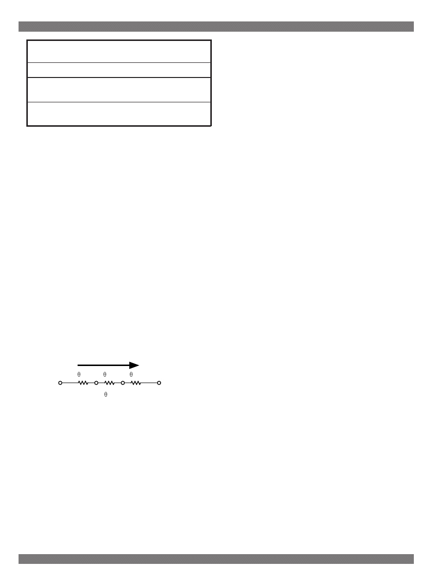
Micrel Semiconductor
Designing With LDO Regulators
Section 3: Using LDO Linear Regulators
48
Designing With Linear Regulators
Thermal
Electrical
Parameter
Parameter
Power (q)
Current (I)
Thermal Resistance
Resistance (R)
(
θ
)
Temperature
Voltage (V)
Difference (
∆
T)
Table 3-6. Thermal/Electrical Analogy
The formula for constant heat flow is:
θ
=
∆
T / q
The equivalent electrical (Ohm’s Law) form is:
I =
∆
V / R
Electrically, a voltage difference across a resis-
tor produces current flow. Thermally, a temperature
gradient across a thermal resistance creates heat
flow. From this, we deduce that if we dissipate power
as heat and need to minimize temperature rise, we
must minimize the thermal resistance. Taken another
way, if we have a given thermal resistance, dissipat-
ing more power will increase the temperature rise.
Thermal resistances act like electrical resis-
tances: in series, they add; in parallel, their recipro-
cals add and the resulting sum is inverted. The gen-
eral problem of heat sinking power semiconductors
may be simplified to the following electrical schematic
(Figure 3-47).
Heat Flow
Die
Ambient
JC
CS
SA
TJ
JA
TA
Figure 3-47. Heat flow through the interface
resistances.
Summing these resistances, the total thermal
path for heat generated by the regulator die is:
θ
JA =
θ
JC +
θ
CS +
θ
SA
Calculating Thermal Parameters
Two types of thermal parameters exist; those
we may control and those fixed by the application (or
physics). The application itself determines which cat-
egory the parameters fit—some systems have a spe-
cific form factor dictated by other factors, for example.
This serves to limit the maximum heat sink size pos-
sible.
Parameter
Extenuating Circumstances
θ
SA
Set by heat sink size, design
and air flow
θ
JC
Set by regulator die size and
package type
θ
CS
Set by mounting technique
and package type
TJ(MAX)
Set by regulator manufac-
turer and lifetime consider-
ations
Power dissipation
Set by VIN, VOUT,
and IOUT
Each regulator data sheet specifies the junction
to case thermal resistance,
θ
JC
.
Heat sink manufac-
turers specify
θ
SA, (often graphically) for each prod-
uct
.
And
θ
CS
is generally small compared to
θ
JC. The
maximum die temperature for Micrel regulators is gen-
erally 125
°
C, unless specified otherwise on the data
sheet. The last remaining variable is the regulator
power dissipation.
Power dissipation in a linear regulator is:
PD = [(VIN – VOUT) IOUT] + (VIN
×
IGND)
Where:
PD = Power dissipation
VIN = Input voltage applied to the regulator
VOUT = Regulator output voltage
IOUT = Regulator output current
IGND = Regulator biasing currents
Proper design dictates use of worst case values
for all parameters. Worst case VIN is high supply.
Worst case VOUT for thermal considerations is the
lowest possible output voltage, subtracting all toler-
ances from the nominal output. IOUT is taken at its
highest steady-state value. The ground current value
comes from the device’s data sheet, from the graph
of IGND vs. IOUT.
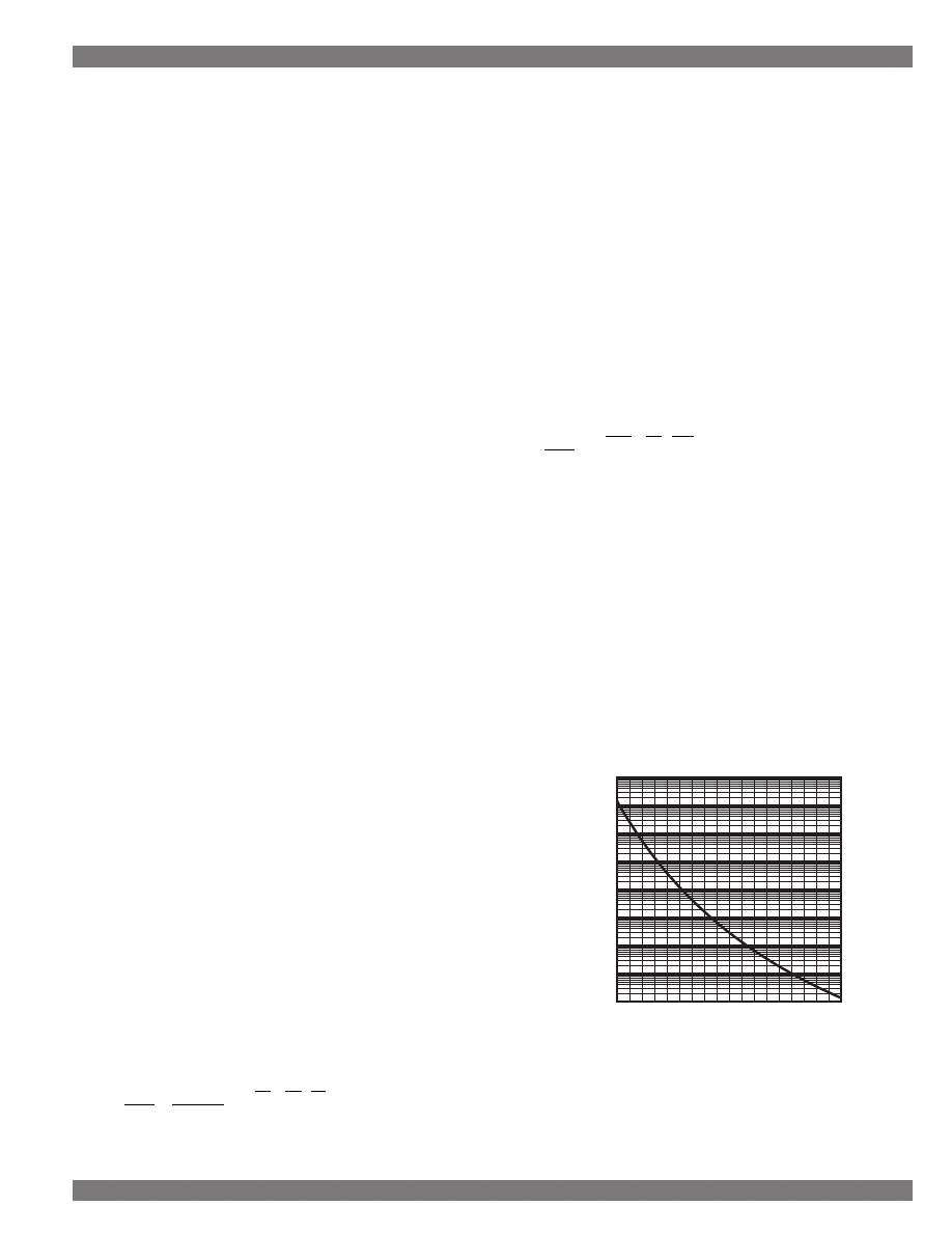
Designing With LDO Regulators
49
Section 3: Using LDO Linear Regulators
Micrel Semiconductor
Designing With LDO Regulators
Calculating Maximum Allowable
Thermal Resistance
Given the power dissipation, ambient operating
temperature, and the maximum junction temperature
of a regulator, the maximum allowable thermal resis-
tance is readily calculated.
θ
JA
≤
(TJ(MAX) – TA) / PD
Maximum heat sink thermal resistance is
θ
SA
≤
θ
JA –
(θ
JC +
θ
CS)
We calculate the thermal resistance (
θ
SA) re-
quired of the heat sink using the following formula:
T
J
– T
A
θ
SA
= –––––––– – (
θ
JC
+
θ
CS
)
P
D
Why A Maximum Junction
Temperature?
Why do semiconductors, including LDO regula-
tors, have a maximum junction temperature (TJ)?
Heat is a natural enemy of most electronic compo-
nents, and regulators are no exception. Semiconduc-
tor lifetimes, statistically specified as mean time to
failure (MTTF) are reduced significantly when they
are operated at high temperatures. The junction tem-
perature, the temperature of the silicon die itself, is
the most important temperature in this calculation.
Device manufacturers have this lifetime-versus-op-
erating temperature trade-off in mind when rating their
devices. Power semiconductor manufacturers must
also deal with the inevitable temperature variations
across the die surface, which are more extreme for
wider temperature-range devices. Also, the mechani-
cal stress induced on the semiconductor, its pack-
age, and its bond wires is increased by temperature
cycling, such as that caused by turning equipment
on and off. A regulator running at a lower maximum
junction temperature has a smaller temperature
change, which creates less mechanical stress.
The expected failure rate under operating con-
ditions is very small, and expressed in FITs (failures
in time), which is defined as failures per one billion
device hours. Deriving the failure rate from the oper-
ating life test temperature to the actual operating tem-
perature is performed using the Arrhenius equation:
100
FR2
MTTF2
MTTF1
Ea
k
1
T2
1
T1
=
=
−
e
Where:
FR1 is the failure rate at temperature T1 (Kelvin)
FR2 is the failure rate at temperature T2
MTTF1 is the mean time to failure at T1
MTTF2 is the mean time to failure at T2
Ea is the activation energy in electron volts (eV)
k is Boltzmann’s constant (8.617386 x 10⁻⁵ eV/K)
The activation energy is determined by long-term
burn-in testing. An average value of 0.62eV is deter-
mined, after considering all temperature-related fail-
ure mechanisms, including silicon-related failure
modes and packaging issues, such as the die attach,
lead bonding, and package material composition.
Using a reference temperature of 125
°
C (498K) and
normalizing to 100 FITs, the formula becomes:
100
FR2
0.62
k
1
T2
1
498
=
−
e
The standard semiconductor reliability versus
junction temperature characteristic is shown in Fig-
ure 3-48. We see that a device operating at 125
°
C
has a relative lifetime of 100. For each 15
°
C rise in
junction temperature, the MTTF halves. At 150
°
C, it
drops to about 34. On the other hand, at 100
°
C, its
life is more than tripled, and at 70
°
C, it is 1800.
As a designer of equipment using LDOs, the
most important rule to remember is “cold is cool; hot
is not”. Minimizing regulator temperatures will maxi-
mize your product’s reliability.
1x10
1
1x10
2
1x10
3
1x10
4
1x10
5
1x10
6
1x10
7
1x10
8
1x10
9
-50 -25
0
25
50
75 100 125 150 175
RELATIVE LIFETIME
JUNCTION TEMPERATURE (
°
C)
Arrhenius Plot
Figure 3-48. Typical MTTF vs. Temperature Curve
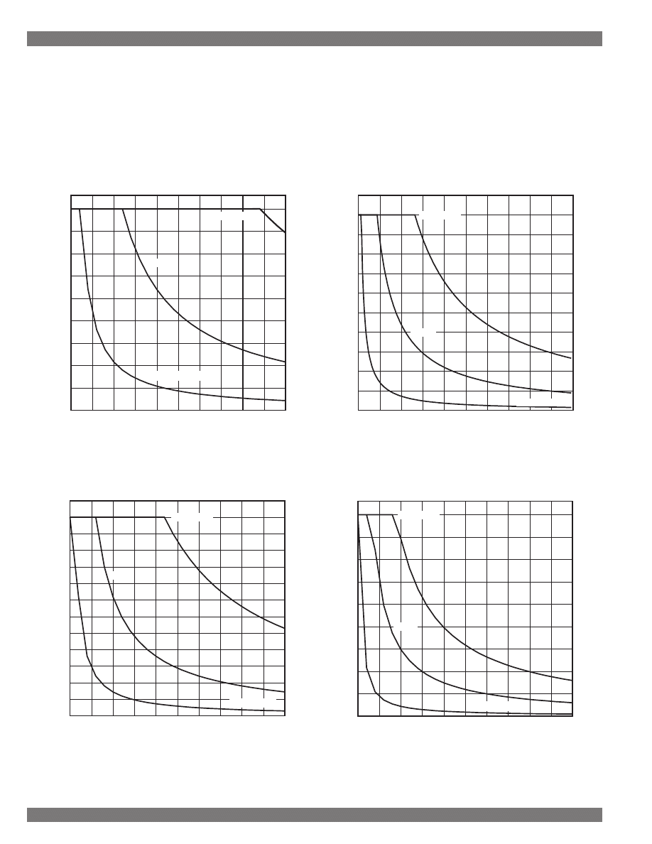
Micrel Semiconductor
Designing With LDO Regulators
Section 3: Using LDO Linear Regulators
50
Designing With Linear Regulators
sink for different input-output voltages at an ambient
temperature of 25
°
C. Three curves are shown: no
heat sink, nominal heat sink, and infinite heat sink
(
θ
SA = 0). Additional thermal design graphs appear
in Section 2.
0
1.0
2.0
3.0
4.0
5.0
0
5
10
15
20
25
OUTPUT CURRENT (A)
V
IN
– V
OUT
MIC29500/29510
Infinite Sink
6
°
C/W
No Heat Sink
Figure 3-51. Maximum Output Current With
Different Heat Sinks, MIC29500 Series
0
2.5
5.0
7.5
0
5
10
15
20
25
OUTPUT CURRENT (A)
V
IN
– V
OUT
MIC29710
Infinite Sink
5
°
C/W
No Heat Sink
Figure 3-52. Maximum Output Current With
Different Heat Sinks, MIC29710/MIC29712
Heat Sink Charts for High Current
Regulators
The heat sink plays an important role in high
current regulator systems, as it directly affects the
safe operating area (SOA) of the semiconductor. The
following graphs, Figure 3-49 through 3-53, show the
maximum output current allowable with a given heat
0
0.5
1.0
1.5
0
5
10
15
20
25
OUTPUT CURRENT (A)
V
IN
– V
OUT
MIC29150
Infinite Sink
8
°
C/W
No Heat Sink
Figure 3-49. Maximum Output Current With
Different Heat Sinks, MIC29150 Series
0
0.5
1.0
1.5
2.0
2.5
3.0
0
5
10
15
20
25
OUTPUT CURRENT (A)
V
IN
– V
OUT
MIC29310
Infinite Sink
8
°
C/W
No Heat Sink
Figure 3-50. Maximum Output Current With
Different Heat Sinks, MIC29300 Series
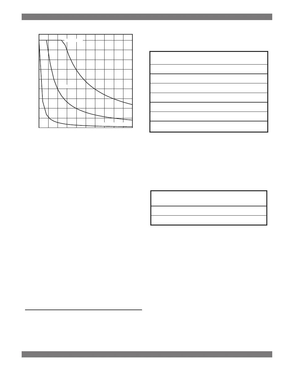
Designing With LDO Regulators
51
Section 3: Using LDO Linear Regulators
Micrel Semiconductor
Designing With LDO Regulators
0
2.5
5.0
7.5
0
5
10
15
20
25
OUTPUT CURRENT (A)
V
IN
– V
OUT
MIC29750
Infinite Sink
4
°
C/W
No Heat Sink
Figure 3-53. Maximum Output Current With
Different Heat Sinks, MIC29750/MIC29752
Thermal Examples
Let’s do an example. We need to design a power
supply for a low voltage microprocessor which re-
quires 3.3V at up to 3A. It will get its input from a 5V
±
5% supply. We choose a MIC29300-3.3BT for our
regulator. The worst case VIN is high supply; in this
case, 5V + 5%, or 5.25V. The LDO has a maximum
die temperature of 125
°
C in its TO-220 package with
a
θ
JC of 2
°
C/W and a mounting resistance (
θ
CS) of
1
°
C/W2, and will operate at an ambient temperature
of 50
°
C. Worst case VOUT for thermal considerations
is minimum, or 3.3V – 2% = 3.234V.5 IOUT is taken
at its highest steady-state value. The ground current
value comes from the device’s data sheet, from the
graph of IGND vs. IOUT.
Armed with this information, we calculate the
thermal resistance (
θ
SA) required of the heat sink
using the previous formula:
125 – 50
°
C
θ
SA
= –––––––––– – (2 + 1
°
C/W) = 4.1
°
C/W
10.5W
Performing similar calculations for 1.25A, 1.5A,
2.0A, 2.5A, 3.0A, 4.0A, and 5.0A gives the results
shown in Table 3-7. We choose the smallest regula-
tor for the required current level to minimize cost.
Regulator
I
OUT
P
D
(W)
θθθθθ
SA
(
°
C/W)
MIC29150
1.25A
2.6
25
MIC29150
1.5A
3.2
21
MIC29300
2.0A
4.2
15
MIC29300
2.5A
5.2
11
MIC29300
3.0A
6.3
8.8
MIC29500
4.0A
8.4
5.9
MIC29500
5.0A
10.5
4.1
Table 3-7. Micrel LDO power dissipation and heat
sink requirements for various 3.3V current levels.
Table 3-8 shows the effect maximum ambient
temperature has on heat sink thermal properties.
Lower thermal resistances require physically larger
heat sinks. The table clearly shows cooler running
systems need smaller heat sinks, as common sense
suggests.
Output
Ambient Temperature
40
°
C
50
°
C
60
°
C
1.5A
24
°
C/W
21
°
C/W
17
°
C/W
5A
5.1
°
C/W
4.1
°
C/W
3.2
°
C/W
Table 3-8. Ambient Temperature Affects Heat Sink
Requirements
Although routine, these calculations become te-
dious. A program written for the HP 48 calculator is
available from Micrel that will calculate any of the
above parameters and ease your design optimiza-
tion process. It will also graph the resulting heat sink
characteristics versus input voltage. See Appendix C
for the program listing or send e-mail to Micrel at
apps@micrel.com
and request program “LDO SINK
for the HP48”.
NOTE 5: Most Micrel regulators are production trimmed to better
than
±
1% accuracy under standard conditions. Across
the full temperature range, with load current and input
voltage variations, the device output voltage varies less
than
±
2%.
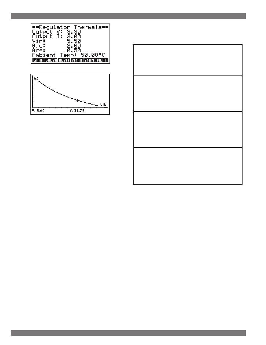
Micrel Semiconductor
Designing With LDO Regulators
Section 3: Using LDO Linear Regulators
52
Designing With Linear Regulators
Figure 3-54. “LDO SINK” Calculator Program Eases
Tedious Thermal Calculations (See Appendix C)
Heat Sink Selection
With this information we may specify a heat sink.
The worst case is still air (natural convection). The
heat sink should be mounted so that at least 0.25
inches (about 6mm) of separation exists between the
sides and top of the sink and other components or
the system case. Thermal properties are maximized
when the heat sink is mounted so that natural verti-
cal motion of warm air is directed along the long axis
of the sink fins.
If we are fortunate enough to have some forced
airflow, reductions in heat sink cost and space are
possible by characterizing air speed–even a slow air
stream significantly assists cooling. As with natural
convection, a small gap allowing the air stream to
pass is necessary. Fins should be located to maxi-
mize airflow along them. Orientation with respect to
vertical is not very important, as airflow cooling domi-
nates the natural convection.
As an example, we will select heat sinks for 1.5A
and 5A outputs. We consider four airflow cases: natu-
ral convection, 200 feet/minute (1m/sec), 300 feet/
minute (1.5m/sec), and 400 feet/minute (2m/sec).
Table 3 shows heat sinks for these air velocities; note
the rapid reduction in size and weight (fin thickness)
when forced air is available. Consulting
manufacturer’s charts, we see a variety of sinks are
made that are suitable for our application. At 5A
(10.5W worst case package dissipation) and natural
convection, sinks are sizable, but at 1.5A (3.2W worst
case package dissipation) and 400 feet/minute air-
flow, modest heat sinks are adequate.
Output Current
Airflow
1.5A
5A
400 ft./min.
Thermalloy 6049PB
Thermalloy 6232
(2m/sec)
Thermalloy 6034
Thermalloy 6391B
300 ft./min.
AAVID 504222B
(1.5m/sec)
AAVID 563202B
AAVID 593202B
AAVID 534302B
Thermalloy 7021B
Thermalloy 6032
Thermalloy 6234B
200 ft./min.
AAVID 508122
(1m/sec)
AAVID 577002
AAVID 552022
Thermalloy 6043PB
AAVID 533302
Thermalloy 6045B
Thermalloy 7025B
Thermalloy 7024B
Thermalloy 7022B
Thermalloy 6101B
Natural
AAVID 576000
AAVID 533602B (v)
Convection
AAVID 574802
AAVID 519922B (h)
(no forced
592502
AAVID 532802B (v)
airflow)
579302
Thermalloy 6299B (v)
Thermalloy 6238B
Thermalloy 7023 (h)
Thermalloy 6038
Thermalloy 7038
Table 3-9. Commercial Heat Sinks for
1.5A and 5.0A Applications [Vertical Mounting
Denoted by (V); (H) Means Horizontal Mounting]
Reading Heat Sink Graphs
Major heat sink manufacturers provide graphs
showing their heat sink characteristics. The standard
graph (Figure 3-55) depicts two different data: one
curve is the heat sink thermal performance in still air
(natural convection); the other shows the performance
possible with forced cooling. The two graphs should
be considered separately since they do not share
common axes. Both are measured using a single
device as a heat source: if multiple regulators are at-
tached, thermal performance improves by as much
as one-third (see
Multiple Packages on One Heat
Sink, below).
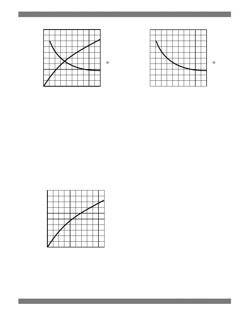
Designing With LDO Regulators
53
Section 3: Using LDO Linear Regulators
Micrel Semiconductor
Designing With LDO Regulators
Power Dissipation (W)
SA
Temperature Rise (
°
C)
Air Velocity (ft/min)
0
20
40
60
80
100
0
2
4
6
8
10
0
2
4
6
8
10
1000
800
600
400
200
0
Figure 3-55. Typical Heat Sink Performance Graph
Figure 3-56 shows the natural convection por-
tion of the curve. The x-axis shows power dissipation
and the y-axis represents temperature rise over am-
bient. While this curve is nearly linear, it does exhibit
some droop at larger temperature rises, represent-
ing increased thermodynamic efficiency with larger
∆
T. At any point on the curve, the
θ
SA is determined
by dividing the temperature rise by the power dissi-
pation.
Figure 3-57 shows the thermal resistance of the
heat sink under forced convection. The x-axis (on top,
by convention) is air velocity in lineal units per minute.
The y-axis (on the right side) is
θ
SA.
Power Dissipation (W)
Temperature Rise (
°
C)
0
20
40
60
80
100
0
2
4
6
8
10
Figure 3-56. Natural Convection Performance
SA
Air Velocity (ft/min)
2
4
6
8
10
0
1000
800
600
400
200
0
Figure 3-57. Forced Convection Performance
Power Sharing Resistor
The heat sink required for 5A applications in still
air is massive and expensive. There is a better way
to manage heat problems: we take advantage of the
very low dropout voltage characteristic of Micrel’s
Super ßeta PNP™ regulators and dissipate some
power externally in a series resistance. By distribut-
ing the voltage drop between this low cost resistor
and the regulator, we distribute the heating and re-
duce the size of the regulator heat sink. Knowing the
worst case voltages in the system and the peak cur-
rent requirements, we select a resistor that drops a
portion of the excess voltage without sacrificing per-
formance. The maximum value of the resistor is cal-
culated from:
V
IN (MIN)
– (V
OUT (MAX)
+ V
DO
)
R
MAX
= ––––––––––––––––––––––
I
OUT (PEAK)
+ I
GND
Where:V
IN (MIN)
is low supply (5V – 5% = 4.75V)
V
OUT (MAX)
is the maximum output voltage
across the full temperature range
(3.3V + 2% = 3.366V)
V
DO
is the worst case dropout voltage across
the full temperature range (600mV)
I
OUT (PEAK)
is the maximum 3.3V load current
I
GND
is the regulator ground current.
For our 5A output example:
4.75 – (3.366 + 0.6) V
0.784V
R
MAX
= –––––––––––––––––– = –––––– = 0.154
Ω
5 + 0.08 A
5.08A
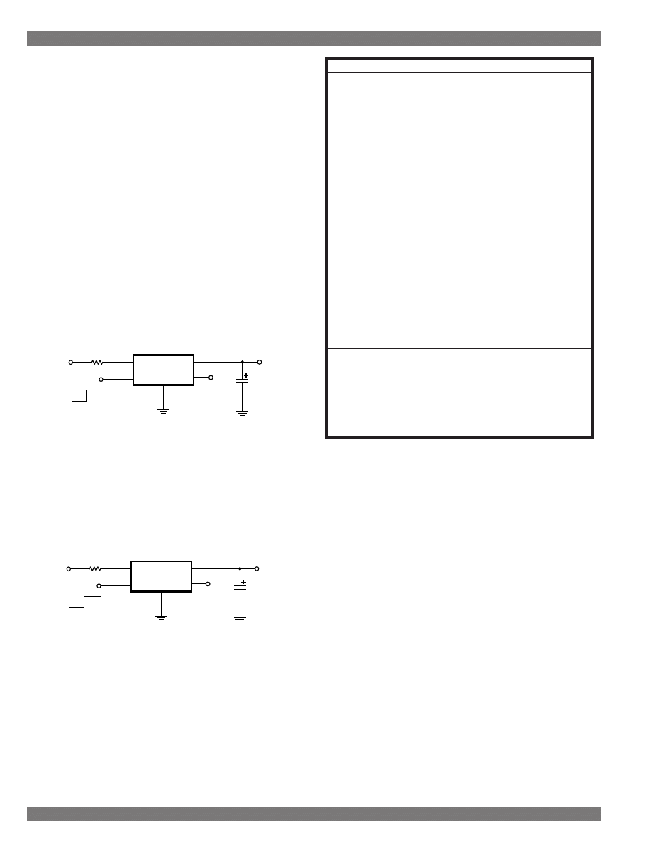
Micrel Semiconductor
Designing With LDO Regulators
Section 3: Using LDO Linear Regulators
54
Designing With Linear Regulators
The power drop across this resistor is:
P
D (RES)
= (I
OUT (PEAK)
+ I
GND
)
2
×
R
or 4.0W. This subtracts directly from the 10.5W of
regulator power dissipation that occurs without the
resistor, reducing regulator heat generation to 6.5W.
P
D(Regulator)
= P
D(R = 0
Ω
)
– P
D (RES)
Considering 5% resistor tolerances and standard
values leads us to a 0.15
Ω
±
5% resistor. This pro-
duces a nominal power savings of 3.9W. With worst-
case tolerances, the regulator power dissipation drops
to 6.8W maximum. This heat drop reduces our heat
sinking requirements for the MIC29500 significantly.
We can use a smaller heat sink with a larger thermal
resistance. Now, a heat sink with 8.3
°
C/W thermal
characteristics is suitable—nearly a factor of 2 better
than without the resistor. Table 3-10 lists representa-
tive heat sinks meeting these conditions.
MIC29501-3.3
Flag
Control
5V
±
5%
0.15
Ω
, 5W
47µF
3.3V
±
1%
@ 5A
≤
0.8V = OFF
≥
2V = ON
Figure 3-58. Resistor Power Sharing Reduces Heat
Sink Requirement
For the 1.5A output application using the
MIC29150, we calculate a maximum R of 0.512
Ω
.
Using R = 0.51
Ω
, at least 1.1W is saved, dropping
power dissipation to only 2.0W—a heat sink is prob-
ably not required. This circuit is shown in Figure 3-
59.
MIC29151-3.3
Flag
Control
5V
±
5%
0.51
Ω
, 2W
22µF
3.3V
±
1%
@ 1.5A
≤
0.8V = OFF
≥
2V = ON
Figure 3-59. Power Sharing Resistor Eliminates
Need for Separate Heat Sink
Another option exists for designers of lower cur-
rent systems. The MIC29150 and MIC29300 regula-
tors are available in the surface mount derivative of
the TO-220 package, the TO-263, which is soldered
directly to the PC board. No separate heat sink is
necessary, as copper area on the board acts as the
heat exchanger. For further information, refer to
Heat
Sinking Surface Mount Packages, which follows.
Airflow
Heat Sink Model
400 ft./min.
AAVID 530700
(2m/sec)
AAVID 574802
Thermalloy 6110
Thermalloy 7137, 7140
Thermalloy 7128
300 ft./min.
AAVID 57302
(1.5m/sec)
AAVID 530600
AAVID 577202
AAVID 576802
Thermalloy 6025
Thermalloy 6109
Thermalloy 6022
200 ft./min.
AAVID 575102
(1m/sec)
AAVID 574902
AAVID 523002
AAVID 504102
Thermalloy 6225
Thermalloy 6070
Thermalloy 6030
Thermalloy 6230
Thermalloy 6021, 6221
Thermalloy 7136, 7138
Natural Convection
AAVID 563202
(no forced airflow)
AAVID 593202
AAVID 534302
Thermalloy 6232
Thermalloy 6032
Thermalloy 6034
Thermalloy 6234
Table 3-10. Representative Commercial Heat Sinks
for the 5.0A Output Example Using a Series
Dropping Resistor (Assumptions: TA = 50
°
C, R =
0.15
Ω
±
5%, IOUT MAX = 5.0A,
θ
JC = 2
°
C/W,
θ
CS
= 1
°
C/W, resulting in a required
θ
SA = 8.0
°
C/W)
Multiple Packages on One Heat Sink
The previous calculations assume the power
dissipation transferred to the heat sink emanates from
a single point source. When multiple heat sources
are applied, heat sink thermal performance (
θ
SA)
improves. Two mechanisms decrease the total effec-
tive thermal resistance:
1. Paralleling multiple devices reduces the
effective
θ
JS.
2. Heat sink efficiency is increased due to
improved heat distribution
Paralleled
θ
JC and
θ
CS terms lead to a reduc-
tion in case temperature of each regulator, since the
power dissipation of each semiconductor is reduced
proportionally. Distributing the heat sources, instead
of a single-point source, minimizes temperature gra-
Designing With LDO Regulators
55
Section 3: Using LDO Linear Regulators
Micrel Semiconductor
Designing With LDO Regulators
dients across the heat sink, resulting in lower con-
duction loss. As much as a 33% reduction in
θ
SA is
possible with distributed heat sources.
Micrel’s Super Beta PNP regulators are a natu-
ral for multiple package mounting on a single heat
sink because their mounting tabs are all at ground
potential. Thus, no insulator is needed between the
package and the heat sink, allowing the best pos-
sible
θ
CS.
Paralleled Devices on a Heat Sink Example
An example will clarify this concept. Given a
regulator that must dissipate 30W of heat, operating
at an ambient temperature of 25
°
C, what heat sink
θ
SA is needed? Given the following parameters:
TJ(MAX) = 125
°
C
θ
JC = 2
°
C/W
θ
CS = 1
°
CW
Case 1: Single Regulator
This configuration is shown graphically in Fig-
ure 3-60.
θ
SA =
∆
T/W – (
θ
JC +
θ
CS)
= (125
°
– 25
°
) / 30W – (2 + 1)
°
C/W
θ
SA = 0.33
°
C/W
This is a very large heat sink.
Die
Ambient
JC
CS
SA
Figure 3-60. Single Heat Source Thermal “Circuit”
Case 2: Two Paralleled Regulators
This configuration is shown graphically in Fig-
ure 3-61. The effective
θ
JS is reduced because the
thermal resistances are connected in parallel.
θ
JC’ = 1/((1/
θ
JC1) + (1/
θ
JC2))
Assuming
θ
JC1 =
θ
JC2, then
θ
JC’ =
θ
JC1
÷
2
= 1
°
C/W
θ
CS’ = 1/((1/
θ
CS1 + (1/
θ
CS2))
Assuming
θ
CS1 =
θ
CS2, then
θ
CS’ =
θ
CS1
÷
2
= 0.5
°
C/W
now
θ
SA =
∆
T/W – (
θ
JC’ +
θ
CS’)
= 1.83
°
C/W
With the 33% efficiency gain, we could use a
heat sink with a
θ
SA rating as high as 2.4
°
C/W. This
represents a tremendous reduction in heat sink size.
Die1
Ambient
JC1
CS1
SA
Die2
JC2
CS2
Figure 3-61. Dual Heat Source Thermal “Circuit”
Case 3: Multiple Paralleled Regulators
This configuration is shown graphically in Fig-
ure 3-62. For the condition of “n” paralleled heat
sources, the
θ
JC and
θ
CS are reduced to 1/n their
per-unit value. The heat sink needs the following rat-
ing:
θ
SA =
∆
T/W – ((
θ
JC1/n) + (
θ
CS1/n))
Die1
Ambient
JC1
CS1
SA
Die n
JC n
CS n
Die 2
JC2
CS2
Figure 3-62. “n” Heat Source Thermal Circuit
Table 3-11 shows the reduction in heat sink per-
formance allowed by paralleled regulators.
n
θθθθθ
SA
1
0.33
2
1.83
3
2.33
4
2.58
5
2.73
6
2.83
Table 3-11. Paralleled Regulators Allow Smaller
(Physical Size) Heat Sinks. TA = 25
°
C

Micrel Semiconductor
Designing With LDO Regulators
Section 3: Using LDO Linear Regulators
56
Designing With Linear Regulators
Another way of looking at this situation is to ask
what is the increase in maximum ambient tempera-
ture paralleled regulators allow?
TA = TJ(MAX) – W
×
[
θ
SA + (
θ
JC/n) + (
θ
CS/n)]
Table 3-12 shows the highest allowable TA us-
ing the 0.33
°
C/W heat sink of Case 1.
n
TA (
°
C)
1
25
2
70
3
85
4
92
5
97
6
100
Table 3-12. Highest Allowable Ambient
Temperature With a 0.33
°
C/W Heat Sink
Heat Sinking Surface Mount Packages
System designers increasingly face the restric-
tion of using all surface-mounted components in their
new designs—even including the power components.
Through-hole components can dissipate excess heat
with clip-on or bolt-on heat sinks keeping things cool.
Surface mounted components do not have this flex-
ibility and rely on the conductive traces or pads on
the printed circuit board for heat transfer. We will ad-
dress the question “How much PC board pad area
does my design require?”
Example 1: TO-263 Package
We will determine if a Micrel surface mount low
dropout linear regulator may operate using only a PC
board pad as its heat sink. We start with the circuit
requirements.
System Requirements:
V
OUT
= 5.0V
V
IN (MAX)
= 9.0V
V
IN (MIN)
= 5.6V
I
OUT
= 700mA
Duty cycle = 100%
T
A
= 50
°
C
This leads us to choose the 750mA MIC2937A-
5.0BU voltage regulator, which has these character-
istics:
V
OUT
= 5V
±
2% (worst case over
temperature)
T
J MAX
= 125
°
C
θ
JC
of the TO-263 = 3
°
C/W
θ
CS
+ 0
°
C/W (soldered directly to board)
Preliminary Calculations
VOUT (MIN) = 5V – 2% = 4.9V
PD = (VIN (MAX) – VOUT (MIN))
×
IOUT + (VIN (MAX)
×
IGND)
= [9V – 4.9V]
×
700mA + (9V
×
15mA) = 3W
Maximum temperature rise,
∆
T = T
J(MAX)
– T
A
= 125
°
C – 50
°
C = 75
°
C
Thermal resistance requirement,
θ
JA
(worst
case):
∆
T = 75
°
C = 25
°
C/W
P
D
3.0W
Heat sink thermal resistance
θ
SA
=
θ
JA
– (
θ
JC
+
θ
CS
)
θ
SA
= 25 – (3 + 0) = 22
°
C/W (max)
Determining Heat Sink Dimensions
Figure 3-63 shows the total area of a round or
square pad, centered on the device. The solid trace
represents the area of a square, single sided, hori-
zontal, solder masked, copper PC board trace heat
sink, measured in square millimeters. No airflow is
assumed. The dashed line shows a heat sink cov-
ered in black oil-based paint and with 1.3m/sec (250
feet per minute) airflow. This approaches a “best case”
pad heat sink.
Conservative design dictates using the solid
trace data, which indicates a pad size of 5000 mm
2
is
needed. This is a pad 71mm by 71mm (2.8 inches
per side).
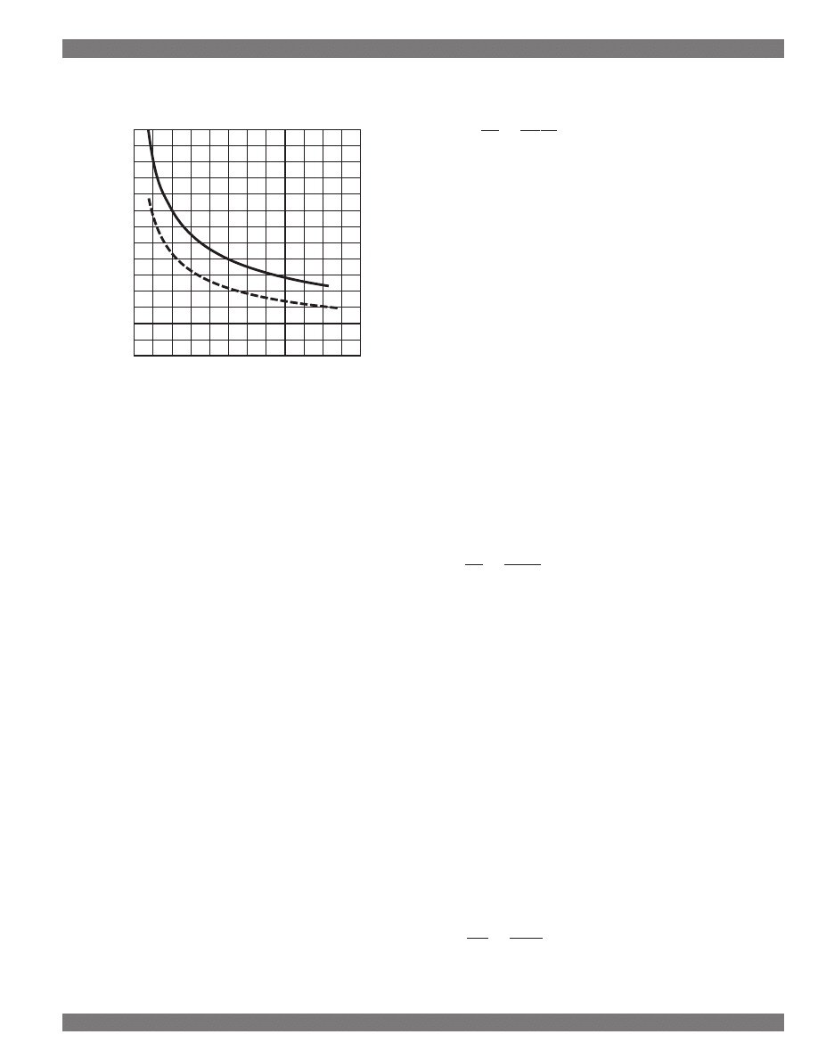
Designing With LDO Regulators
57
Section 3: Using LDO Linear Regulators
Micrel Semiconductor
Designing With LDO Regulators
0
10
20
30
40
50
60
70
0
2000
4000
6000
PCB Heat Sink Thermal Resistance (
°
C/W)
PCB Heat Sink Area (mm
2
)
PC Board Heat Sink
Thermal Resistance vs. Area
Figure 3-63. Graph to Determine PC Board Area
for a Given Thermal Resistance (See text for
Discussion of the Two Curves)
Example 2: SO-8 and SOT-223 Package
Given the following requirements, determine the
safe heat sink pad area.
V
OUT
= 5.0V
V
IN (MAX)
= 14V
V
IN (MIN)
= 5.6V
I
OUT
= 150mA
Duty cycle = 100%
T
A
= 50
°
C
Your board production facility prefers handling
the dual-in-line SO-8 packages whenever possible.
Is the SO-8 up to this task? Choosing the MIC2951-
03BM, we get these characteristics:
T
J (MAX)
= 125
°
C
θ
JC
°
C/W
SO-8 Calculations:
P
D
= [14V – 5V]
×
150mA + (14V
×
8mA
)
= 1.46W
Temperature rise = 125
°
C – 50
°
C = 75
°
C
Thermal resistance requirement,
θ
JA
(worst
case):
∆
T = 75
°
C = 51.3
°
C/W
P
D
1.46W
Heat sink
θ
SA
= 51 – 100 = –49
°
C/W (max)
The negative sign flags the problem: without re-
frigeration, the SO-8 is not suitable for this applica-
tion. Consider the MIC5201-5.0BS in a SOT-223
package. This package is smaller than the SO-8, but
its three terminals are designed for much better ther-
mal flow. Choosing the MIC5201-3.3BS, we get these
characteristics:
T
J (MAX)
= 125
°
C
θ
JC
°
C/W
θ
CS
= 0
°
C/W (soldered directly to board)
P
D
= [14V – 4.9V]
×
150mA + (14V
×
1.5mA)
= 1.4W
Temperature rise = 125
°
C – 50
°
C = 75
°
C
Thermal resistance requirement,
θ
JA
(worst case):
∆
T = 75
°
C = 54
°
C/W
P
D
1.4W
Heat sink
θ
SA
= 54 – 15 = 39
°
C/W (max)
Board Area
Referring to Figure 3-63, a pad of 1400mm2 (a
square pad 1.5 inches per side) provides the required
thermal characteristics.
Example 3: SOT-23-5 Package
A regulator for a cellular telephone must provide
3.6V at 50mA from a battery that could be as high as
6.25V. The maximum ambient temperature is 70
°
C
and the maximum desired junction temperature is
100
°
C. The minimum-geometry thermal capability of
the MIC5205 in the SOT-23-5 is 220
°
C/W; must we
provide additional area for cooling?
PD= [6.25 – 3.56V]
×
50mA + (6.25V
×
0.35mA)
= 137mW
∆
T = 30
°
C
= 219
°
C/W
P
D
0.137W
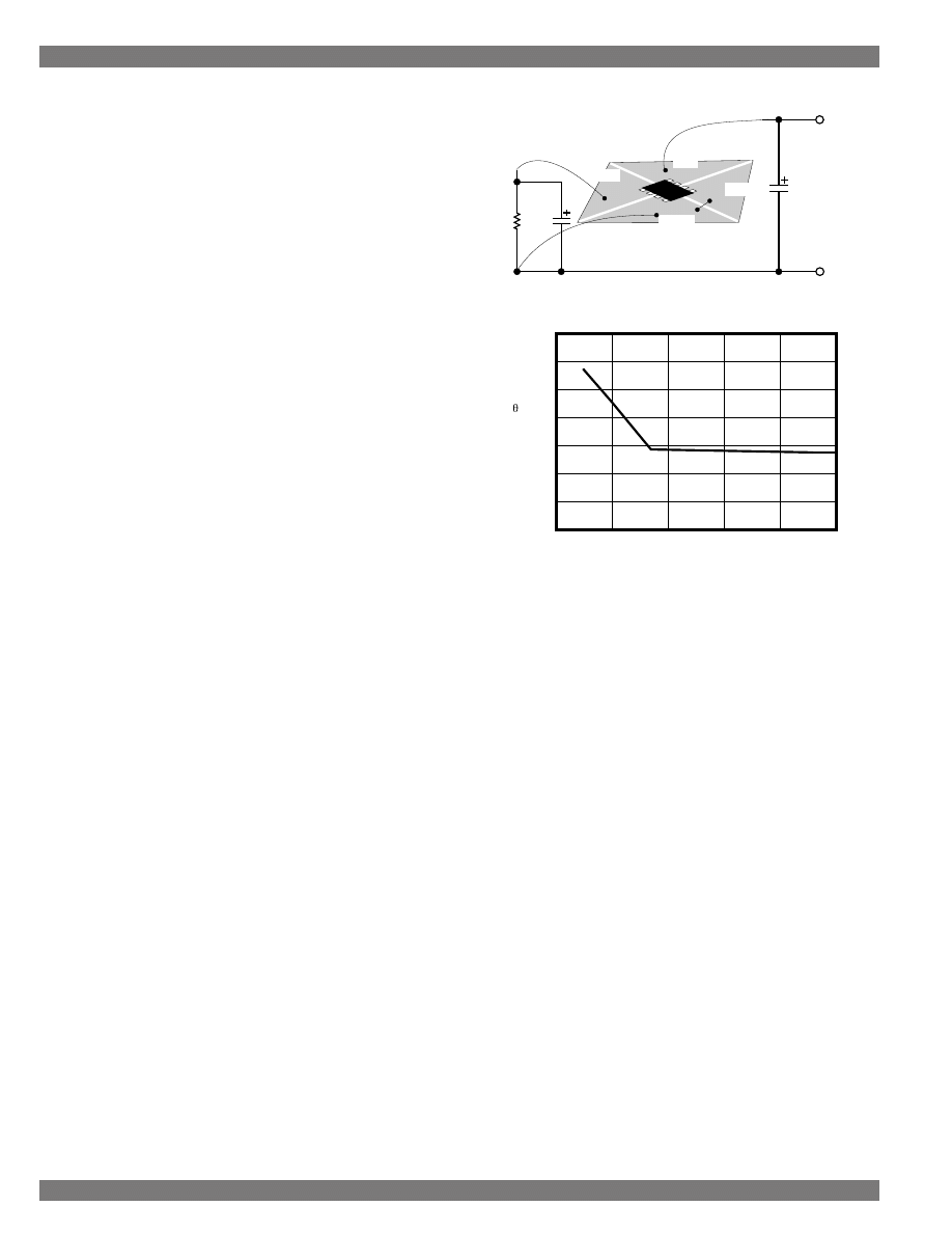
Micrel Semiconductor
Designing With LDO Regulators
Section 3: Using LDO Linear Regulators
58
Designing With Linear Regulators
Which is close enough to 220
°
C/W
θ
JA for our
purposes. We can use the minimum-geometry lay-
out.
If our electrical or thermal parameters worsened,
we could refer to Figure 3-63 and determine the ad-
ditional copper area needed for heat sinking. Use a
value of 130
°
C/W
θ
JC for the MIC5205-xxBM5.
Example 4, Measurement of
θθθθθ
An MIC5206-3.6BMM (in the 8-pin MSOP pack-
age) was soldered to 1oz. double-sided copper PC
board material. The board, measuring 4.6 square
inches, had its top layer sliced into four quadrants,
corresponding to input, output, ground, and enable
(see Figure 3-64), and a temperature probe was sol-
dered close to the regulator. The device thermal shut-
down temperature was measured at zero power dis-
sipation to give an easy-to-detect temperature refer-
ence point. The device was cooled, then the load was
increased until the device reached thermal shutdown.
By combining TA, TJ (SHUTDOWN), and PD, we may
accurately determine
θ
JA as:
θ
JA = (TJ (SHUTDOWN) – TA)
÷
PD
For a given board size. Next, the board was
trimmed to about 2 square inches and retested. Mea-
surements were also taken at 1 and 0.5 square
inches. The results are shown in Figure 3-65.
Board interconnect wires are #30 (AWG)
Input
Output
Ground
Enable
RL
+13.6V
Figure 3-64. MSOP-8 Thermal Resistance Test Jig
180
170
110
120
130
140
150
160
0
5
4
3
2
1
Board Size, Square Inches
JA
(
°
C/W)
Figure 3-65. Junction to Ambient Thermal
Resistance for the MSOP-8 Package
Comments
These formulas are provided as a general guide
to thermal characteristics for surface mounted power
components. Many estimations and generalizations
were made; your system will vary. Please use this
information as a rough approximation of board area
required and fully evaluate the thermal properties of
each board you design to confirm the validity of the
assumptions.
Designing With LDO Regulators
59
Section 3: Using LDO Linear Regulators
Micrel Semiconductor
Designing With LDO Regulators
Linear Regulator Troubleshooting Guide
Solutions to each of these possible causes are presented earlier in this section. If problems persist,
please contact Micrel Applications Engineering for assistance.
Problem
Possible Cause
Output Voltage Low at Heavy Load
Regulator in dropout
Excessive lead resistance between regulator
and load
Regulator in current limit
Regulator in thermal shutdown
Output Voltage Bad at Light Load
Regulator in Dropout
Minimum output load current not satisfied
Input voltage too high (overvoltage shutdown)
Layout problem
Regulator Oscillates
Output capacitor too small (Super
β
eta PNP)
Output capacitor ESR too small
Input capacitor bad or missing
Layout problems
Regulator Does Not Start
Output polarity reversed
Input voltage too high (overvoltage shutdown)
Load is shorted or latched up
AC Ripple on Output
Ground loop with input filter capacitor

Micrel Semiconductor
Designing With LDO Regulators
Section 4: Linear Regulator Solutions 60 Designing With LDO Regulators
Section 4. Linear Regulator Solutions
• MIC2920A — family of 400mA regulators in TO-
220, TO-263-3, SOT-223, and SO-8 packages.
Fixed output voltages of 3.3V, 4.85V, 5V, and 12V
plus three adjustable versions are available.
• MIC2937A — family of 750mA regulators in TO-
220 and TO-263 packages. Fixed output volt-
ages of 3.3V, 5V, and 12V, plus two adjustable
versions are available.
• MIC2940A — 1250mA regulators in TO-220 and
TO-263 packages with fixed output voltages of
3.3V, 5V, and 12V. The MIC2941A is an adjust-
able version.
• MIC29150 — family of 1.5A regulators in TO-
220 and TO-263 packages. Fixed output volt-
ages of 3.3V, 5V, and 12V, plus two adjustable
versions are available.
• MIC29300 — family of 3A regulators in TO-220
and TO-263 packages. Fixed output voltages of
3.3V, 5V, and 12V, plus two adjustable versions
are available.
• MIC29310 — low-cost 3A regulator with 3.3 and
5V fixed outputs in a TO-220 package. The
MIC29312 is an adjustable version.
• MIC29500 — family of 5A regulators in TO-220,
and TO-263 packages. Fixed output voltages of
3.3V and 5V, plus two adjustable versions are
available.
• MIC29510 — low-cost 5A regulator with 3.3 and
5V fixed outputs in a TO-220 package. The
MIC29512 is an adjustable version.
• MIC29710 — low-cost 7.5A regulator with 3.3
and 5V fixed outputs in a TO-220 package. The
MIC29712 is an adjustable version.
• MIC29750 — 7.5A regulator in a TO-247 power
package with 3.3 and 5V fixed outputs. The
MIC29752 is an adjustable version.
Micrel’s medium and high-current regulators
(400mA and higher output current capability) have a
part numbering code that denotes the additional fea-
tures offered. The basic family number, ending in “A”
or “0” denotes the easy-to-use three-pin fixed volt-
age regulator.
Super
β
eta PNP™ Regulators
Micrel’s easy to use Super ßeta PNP™ LDO
monolithic regulators deliver highly accurate output
voltages and are fully protected from fault conditions.
Their maximum output currents range from 80mA to
7.5A. They are available in numerous fixed voltages,
and most families offer adjustable versions.
Micrel’s monolithic linear regulator family ap-
pears below, listed by increasing output current ca-
pability.
•
• MIC5203 — 80mA regulator in the tiny SOT-143
package. Fixed output voltages of 2.85, 3.0,
3.3, 3.6, 3.8, 4.0, 4.75, and 5.0V are available.
• LP2950 — 100mA fixed 3.3, 4.85, and 5.0V
regulator available in the TO-92 package.
• LP2951 — 100mA fixed 5.0V and adjustable
regulator available in the SO-8 package.
• MIC5200 — 100mA regulator available in SO-8
and SOT-223 packages. Fixed output voltages
of 3.0, 3.3, 4.85, and 5.0V are available.
• MIC5202 — dual 100mA version of the ‘5200,
available in the SO-8 package.
• MIC5205 — 150mA low-noise fixed and adjust-
able regulator supplied in the small SOT-23-5
package.
• MIC5206 — 150mA low-noise regulator sup-
plied in the small SOT-23-5 or MSOP-8
packages.
• MIC5207 — 180mA low-noise regulator sup-
plied in the small SOT-23-5 or TO-92 packages.
• MIC2950 — 150mA fixed 3.3, 4.85, and 5.0V
regulator available in the TO-92 package.
• MIC2951 — 150mA fixed 5.0V and adjustable
regulator available in the SO-8 package.
• MIC5201 — 200mA regulator available in SO-8
and SOT-223 packages. Fixed output voltages
of 3.0, 3.3, 4.85, and 5V, plus an adjustable ver-
sion are available.
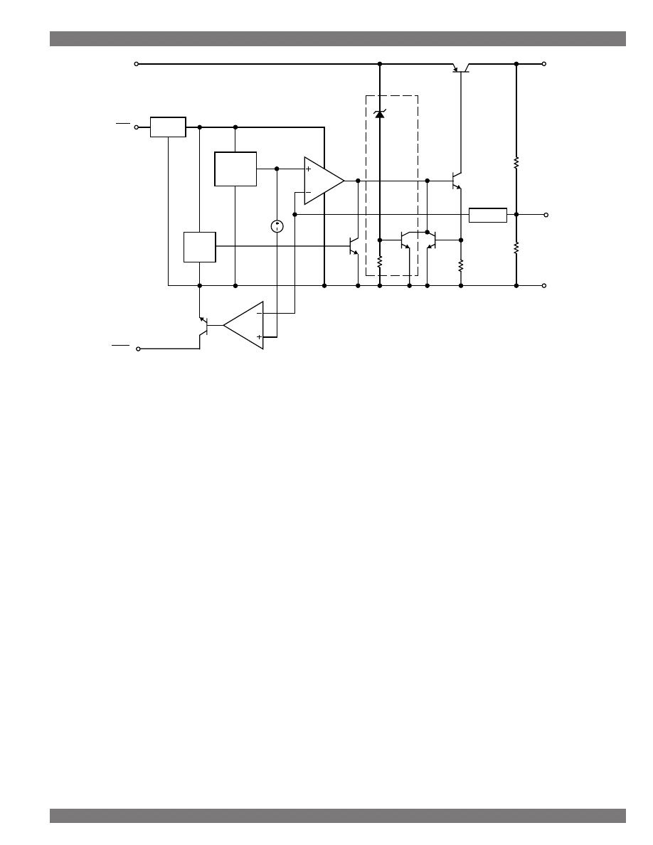
Designing With LDO Regulators
61
Section 4: Linear Regulator Solutions
Micrel Semiconductor
Designing With LDO Regulators
•
Part numbers ending in “1” are five-pin fixed de-
vices with a digital control pin for turning the
regulator ON or OFF and an Error Flag output
that signals when the output is not in regulation.
•
Part numbers ending in “2” are adjustable parts
with ON/OFF control.
•
Devices ending with “3” are adjustables with an
Error Flag.
Super
β
eta PNP Circuitry
The simplified schematic diagram of Micrel’s me-
dium and high current monolithic LDOs appears as
Figure 4-1. The high current path from input to output
through the pass transistor is in bold. The bandgap
reference and all other circuitry is powered via the
Enable Circuit, which allows for “zero” current draw
when disabled. The reference voltage is compared
to the sampled output voltage fed back by R1 and
R2. If this voltage is less than the bandgap reference,
the op amp output increases. This increases the cur-
rent through driver transistor Q2, which pulls down
on the base of Q1, turning it on harder. If Q1’s base
current rises excessively, the voltage drop across R3
enables Q3, which in turn limits the current through
Q2. Die temperature is monitored, and if it becomes
excessive, the thermal shutdown circuit activates,
clamping the base of Q2 and shutting down Q1. The
flag circuit looks at the output voltage sample and
compares it to a reference set 5% lower. If the sample
is even lower, the flag comparator saturates the open
collector flag transistor, signaling the fault condition.
Dropout Voltage
The Super
β
eta PNP family of low-dropout regu-
lators offers typical dropout voltages of only 300mV
across the output current range. This low dropout is
achieved by using large and efficient multicelled PNP
output transistors, and operating them in their high-
beta range well below their capacity. Dropout voltage
in the Super
β
eta PNP regulators is determined by
the saturation voltage of the PNP pass element. As
in all bipolar transistors, the saturation voltage is pro-
portional to the current through the transistor. At light
loads, the dropout voltage is only a few tens of milli-
volts. At moderate output currents, the dropout rises
to 200 to 300mV. At the full rated output, the typical
dropout voltage is approximately 300mV for most of
the families. Lower cost versions have somewhat
higher dropout at full load, generally in the 400 to
ON/OFF
Band-gap
Reference
Bias
Feedback
GND
28V
OUT
ON/OFF
V
IN
O.V. I
LIMIT
Thermal
Shut
Down
FLAG
R1
R2
Q2
Q3
R3
Q1
ADJ
1.240V
1.180V
Flag Comparator
Figure 4-1. Super ßeta PNP™ Regulator Simplified Schematic Diagram

Micrel Semiconductor
Designing With LDO Regulators
Section 4: Linear Regulator Solutions
62
Designing With LDO Regulators
500mV range. The data sheet for each device graphs
typical dropout voltage versus output current.
Ground Current
Micrel’s Super
β
eta PNP process allows these
high current devices to maintain very high transistor
beta—on the order of 100 at their full rated current.
This contrasts with competitive PNP devices that suf-
fer with betas in the 10 to 30 range. This impacts
regulator designs by reducing wasteful ground cur-
rent. Micrel’s beta of 100 translates into typical full
load ground currents of only 1% of your output. The
data sheet for each device graphs typical ground cur-
rent versus output current.
When linear regulators approach dropout, gen-
erally due to insufficient input voltage, base drive to
the pass transistor increases to fully saturate the tran-
sistor. With some older PNP regulators, the ground
current would skyrocket as dropout approached.
Micrel’s Super
β
eta PNP regulators employ satura-
tion detection circuitry which limits base drive when
dropout-induced saturation occurs, limiting ground
current.
Fully Protected
Micrel regulators are survivors. Built-in protec-
tion features like current limiting, overtemperature
shutdown, and reversed-input polarity protection al-
low LDO survival under otherwise catastrophic situa-
tions. Other protection features are optionally avail-
able, such as overvoltage shutdown and a digital er-
ror flag.
Current Limiting
Current limiting is the first line of defense for a
regulator. It operates nearly instantaneously in the
event of a fault, and keeps the internal transistor, its
wire bonds, and external circuit board traces from
fusing in the event of a short circuit or extremely heavy
output load. The current limit operates by linearly
clamping the output current in case of a fault. For
example, if a MIC29150 with a 2A current limit en-
counters a shorted load, it will pass up to 2A of cur-
rent into that load. The resulting high power dissipa-
tion (2A multiplied by the entire input voltage) causes
the regulator’s die temperature to rise, triggering the
second line of defense, overtemperature shutdown.
Overtemperature Shutdown
As the output fault causes internal dissipation
and die temperature rise, the regulator approaches
its operating limits. At a predetermined high tempera-
ture, the regulator shuts off its pass element, bring-
ing output current and power dissipation to zero. The
hot die begins cooling. When its temperature drops
below an acceptable temperature threshold, it auto-
matically re-enables itself. If the load problem has
been addressed, normal operation resumes. If the
short persists, the LDO will begin sourcing current,
will heat up, and eventually will turn off again. This
sequence will repeat until the load is corrected or in-
put power is removed. Although operation at the verge
of thermal shutdown is not recommended, Micrel has
tested LDOs for several million ON/OFF thermal
cycles without undue die stress. In fact, during reli-
ability testing, regulators are burned-in at the ther-
mal shutdown-cycle limit.
Reversed Input Polarity
Protection from reversed input polarity is impor-
tant for a number of reasons. Consumer products
using LDOs with this feature survive batteries inserted
improperly or the use of the wrong AC adapter. Auto-
motive electronics must survive improper jump start-
ing. All types of systems should last through initial
production testing with an incorrectly inserted (back-
ward) regulator. By using reversed input protected
regulators, both the regulator and its load are pro-
tected against reverse polarity, which limits reverse
current flow.
This feature may be simulated as an ideal di-
ode,
with zero forward voltage drop, in series with
the output. Actually, a small current flows from the
input pin to ground through the voltage divider net-
work, but this may generally be neglected. Measured
data from Super ßeta PNP regulators with a 100
Ω
resistor from output to ground follows:
Input Voltage (V)
Load Current (mA)
0
0
–5
0
–10
0
–15
–2.0
–20
–6.9
–25
–7.8
–30
–14
Although the devices were tested to –30V for
this table without any failure, the reverse-polarity
specification ranges only to –20V.
Designing With LDO Regulators
63
Section 4: Linear Regulator Solutions
Micrel Semiconductor
Designing With LDO Regulators
Overvoltage Shutdown
Most Micrel LDOs feature overvoltage shutdown.
If the input voltage rises above a certain predeter-
mined level, generally between 35V and 40V, the
control circuitry disables the output pass transistor.
This feature allows the regulator to reliably survive
high voltage (60V or so—see the device data sheet
for the exact limit) spikes on the input regardless of
output load conditions. The automotive industry calls
this feature “Load-Dump Protection”
1
and it is crucial
to reliability in automotive electronics.
Many of Micrel’s regulator families offer a ver-
sion with a digital error flag output. The error flag
monitors the output voltage and pulls its open collec-
tor (or drain) output low if the voltage is too low. The
definition of “too low” ranges from about –5% to –8%
below nominal output, depending upon the device
type. The flag comparator is unaffected by low input
voltage or a too-light or too-heavy load (although a
too-heavy load generally will cause the output volt-
age to drop, triggering the flag).
Variety of Packages
From the tiny SOT-143 to the large TO-247 (also
known as the TO-3P), Micrel Super ßeta PNP regu-
lators span orders of magnitude in both size and out-
put current.
Why Choose Five Terminal Regulators?
What do the extra pins of the five pin linear regu-
lators provide? After all, three terminal regulators give
Input, Output, and Ground; what else is necessary?
Five terminal devices allow the system designer to
monitor power quality to the load and digitally switch
the supply ON and OFF. Power quality is indicated
by a flag output. When the output voltage is within a
few percent of its desired value, the flag is high, indi-
cating the output is good. If the output drops, because
of either low input voltage to the regulator or an over-
current condition, the flag drops to signal a fault con-
dition. A controller can monitor this output and make
decisions regarding the system’s readiness. For ex-
ample, at initial power-up, the flag will instantaneously
read high (if pulled up to an external supply), but as
soon as the input supply to the regulator reaches
about 2V, the flag pulls low. It stays low until the regu-
lator output nears its desired value. With the
MIC29150 family of low-dropout linear regulators, the
flag rises when the output voltage reaches about 97%
of the desired value. In a 3.3V system, the flag indi-
cates “output good” with V
OUT
= 3.2V.
Logic-compatible power control allows “sleep”
mode operation and results in better energy efficiency.
The ENABLE input of the MIC29150 family is TTL
and 5V or 3.3V CMOS compatible. When this input is
pulled above approximately 1.4V, the regulator is
activated. A special feature of this regulator family is
zero power consumption when inactive. Whenever
the logic control input is low, all internal circuitry is
biased OFF. (A tiny leakage current, measured in
nanoamperes, may flow).
Three terminal regulators are used whenever
ON/OFF control is not necessary and no processing
power is available to respond to the flag output infor-
mation. Three terminal regulators need only a single
output filter capacitor minimizing design effort. Micrel
three-terminal regulators all are fixed-output voltage
devices with the same pin configuration: input, ground,
output.
Five terminal regulators provide all the function-
ality of three pin devices PLUS allow power supply
quality monitoring and ON/OFF switching for “sleep”
mode applications.
Compatible Pinouts
Micrel’s MIC29150/29300/29500 and MIC29310/
29510/29710 families of low-dropout regulators have
identical pinouts throughout the line. A single board
layout accommodates from 1.5A through 7.5A of maxi-
mum current, simply by replacing one LDO with an-
other of different rating. Additionally, the three pin and
five pin versions of these two families have a similar-
ity that allows a three pin regulator to function in a
socket designed for a five pin version.
Three Pin Regulator
Five Pin Regulator
—
Enable or Flag
Input
Input
Ground
Ground
Output
Output
—
Adjust or Flag
Many applications do not require the ENABLE
or FLAG functions. In these cases, if a fixed voltage
is suitable, a three pin LDO may be substituted in the
NOTE 1: A “load dump” fault occurs in an automobile when the
battery cable breaks loose and the unfiltered alternator
output powers the vehicle.
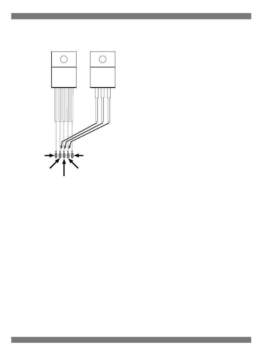
Micrel Semiconductor
Designing With LDO Regulators
Section 4: Linear Regulator Solutions
64
Designing With LDO Regulators
five pin socket by simply leaving the outer holes open.
Use care when forming the leads; gently bend them
90
°
before compressing them. The plastic may crack
if the leads are forced excessively.
MIC29151-xx
MIC29152
MIC29301-xx
MIC29302
MIC29501-xx
MIC29502
MIC29150-xx
MIC29300-xx
MIC29500-xx
Figure 4-2. PC Board Layout for 5-Pin
and 3-Pin Regulators
Stability Issues
PNP output regulators require a minimum value
of output filter capacitance for stability. The data sheet
for each device specifies the minimum value of out-
put capacitor necessary.
A stability analysis of the PNP regulators shows
there are two main poles, one low internal pole at
about 10Hz, and an external pole provided by the
output filter capacitor. An internal zero of approxi-
mately 1.5kHz cancels the internal pole, leaving the
output capacitor to provide the dominant pole for sta-
bility. Gain/phase characteristics are affected by sev-
eral parameters:
•
Internal design
(compensation and configuration)
•
Load capacitor value
•
Load capacitor ESR
•
Load current
•
Output transistor beta
•
Driver stage transconductance
Stray capacitance on the feedback pins of ad-
justable regulators serves to decrease the phase
margin. Circuits designed for minimum output noise
often intentionally add capacitance across a feedback
resistor, which couples back to the feedback pin. In-
creasing the size of the output filter capacitor in this
situation recovers the phase margin required for sta-
bility.
Paralleling Bipolar Regulators
The most difficult aspect of using linear regula-
tors is heat sinking. As output current and/or input-to-
output voltage differential increases, the heat sink size
rapidly increases. One method of mitigating this is to
split the heat into more than one point source. In Sec-
tion 3,
Thermal Management, using a resistor to dis-
sipate excess power when the input voltage is much
higher than the desired output was discussed, but
this technique is unusable when we need low system
dropout. Another method of power sharing is to par-
allel the regulators. This preserves their low dropout
characteristics and also allows scaling to higher out-
put currents. As also shown in
Thermal Management,
heat sinking two devices is up to 33% more efficient
than sinking one at the same overall power level.
Bipolar transistors have a negative temperature
coefficient of resistance; as they get hotter, they pass
more current for a given voltage. This characteristic
makes paralleling bipolar transistors difficult—if the
transistors are not precisely matched and at identical
temperatures, one will draw more current than the
others. This transistor will thereby get hotter and draw
even more current. This condition, known as thermal
runaway, prevents equal current sharing between de-
vices and often results in the destruction of the hot-
test device.
We may parallel bipolar transistors if we moni-
tor the current through each of the devices and some-
how force them to be equal. An easy and accurate
method is by using current sense resistors and op
amps. Figure 4-3 shows two 7.5A MIC29712 in par-
allel to produce a 15A composite output. One regula-
tor is chosen as the master. Its output is adjusted to
the desired voltage in the usual manner with two re-
sistors. A small-value sense resistor samples the out-
put for the op amp. The resistor value is chosen to
provide an output voltage large enough to swamp the
input offset voltage (V
OS
) of the op amp with medium
output current. If the resistor is too small, matching
will be poor; if it is too large, system dropout voltage
Designing With LDO Regulators
65
Section 4: Linear Regulator Solutions
Micrel Semiconductor
Designing With LDO Regulators
Figure 4-4. Three or More Parallel Super ßeta PNP Regulators
MIC29712
(Slave 1)
10m
Ω
10k
Ω
0.01µF
MIC6211
3
4
1
5
2
+ VIN
MIC29712
(Master)
10m
Ω
330µF
68µF
4V to 6V
3.3V at 22.5A
MIC29712
(Slave 2)
10m
Ω
10k
Ω
0.01µF
MIC6211
3
4
1
5
2
+ VIN
R1 205k
Ω
R2
124k
Ω
VOUT = 1.240
×
(1 + R1/R2)
VIN
VOUT
EN
ADJ
GND
VIN
VOUT
EN
ADJ
GND
VIN
VOUT
EN
ADJ
GND
will increase. The op amp drives the ADJ input of the
slave regulator and matches its output to the master.
This technique is also applicable to three or more
paralleled regulators: Figure 4-4 shows three in par-
allel. This may be extended to any number of de-
vices by merely adding a sense resistor and op amp
circuit to each additional slave regulator.
Although a fixed regulator can be used as a
master, this is not recommended. Load regulation
suffers because fixed output regulators (usually) do
not have a separate SENSE input to monitor load
voltage. As current through the sense resistor in-
creases, the output voltage will drop because volt-
age sensing occurs on the wrong side of the current
sense resistor.
MIC29712
(Master)
MIC29712
(Slave)
10m
Ω
10m
Ω
10k
Ω
0.01µF
220µF
47µF
4V to 6V
3.3V at 15A
MIC6211
3
4
1
5
2
+ VIN
R1 205k
Ω
R2
124k
Ω
VOUT = 1.240
×
(1 + R1/R2)
VIN
VOUT
EN
ADJ
GND
VIN
VOUT
EN
ADJ
GND
Figure 4-3. Two Super ßeta PNP Regulators in Parallel
Micrel Semiconductor
Designing With LDO Regulators
Section 4: Linear Regulator Solutions
66
Designing With LDO Regulators
Micrel’s Unique “Super LDO™”
The Super LDO™ is a dedicated control IC to
drive an external N-channel MOSFET pass element.
It allows economical management of moderate to high
output currents.
The external pass element offers the designer
three advantages unattainable with the monolithic
approach: First, because the control circuitry is sepa-
rate, the pass element’s die area in a given package
can be increased. This results in lower dropout volt-
ages at higher output currents. Second, the junction-
to-case thermal resistance is much less allowing
higher output currents before a heat sink is required.
Third, the semiconductor process for manufacturing
MOSFETs is simpler and less costly than the pro-
cess needed to fabricate accurate voltage references
and analog comparators. High current monolithic
regulators have most of their die area dedicated to
the output device; why build a large, relatively simple
device on an expensive process? The Super LDO
combines all three advantages to produce a high
performance, low cost regulating system.
V
REF
V
IN
+ 10V
N-channel
V
IN
V
OUT
Figure 4-5. N-Channel Regulator
The most attractive device for the external pass
element is the N-channel power MOSFET (see Fig-
ure 4-5). Discrete N-channel MOSFET prices con-
tinue to decrease (due to high volume usage), and
the race for lower and lower ON resistance works in
your favor. The N-channel MOSFET, like the
P-channel MOSFET, reduces ground current. With
device ON resistance now below 10m
Ω
, dropout volt-
ages below 100mV are possible with output currents
in excess of 10A. Even lower dropouts are possible
by using two or more pass elements in parallel.
Unfortunately, full gate-to-source enhancement
of the N-channel MOSFET requires an additional 10V
to 15V above the required output voltage. Control-
ling the MOSFET’s gate using a second higher volt-
age supply requires additional circuitry and is clumsy
at best.
Micrel’s Super LDO Family
Micrel’s Super LDO Regulator family consists
of three regulators which control an external
N-channel MOSFET for low dropout at high current.
Two members of the family internally generate the
required higher MOSFET enhancement voltage, while
the other relies on an existing external supply volt-
age.
All members of the Super LDO Regulator family
have a 35mV current limit threshold,
±
2% nominal
output voltage setting, and a 3V to 36V operating
voltage range. All family members also include a TTL
compatible enable/shutdown input (EN) and an open
collector fault output (FLAG). When shutdown (TTL
low), the device draws less than 1
µ
A. The FLAG out-
put is low whenever the output voltage is 6% or more
below its nominal value.
The MIC5156
The MIC5156 Super LDO Regulator occupies
the least printed circuit board space in applications
where a suitable voltage is available for MOSFET gate
enhancement. To minimize external parts, the
MIC5156 is available in fixed output versions of 3.3V
or 5V. An adjustable version is also available which
uses two external resistors to set the output voltage
from 1.3V to 36V.
The MIC5157 and MIC5158
For stand-alone applications the MIC5157 and
MIC5158 incorporate an internal charge-pump volt-
age tripler to supply the necessary gate enhancement
for an external N-channel MOSFET. Both devices can
fully enhance a logic-level N-channel MOSFET from
a supply voltage as low as 3.0V. Three inexpensive
small value capacitors are required by the charge
pump.
The MIC5157 output voltage is externally se-
lected for a fixed output voltage of 3.3V, 5V or 12V.
The MIC5158 output voltage is externally select-
able for either a fixed 5V output or an adjustable out-
put. Two external resistors are required to set the
output voltage for adjustable operation.
3.3V, 10A Regulator Application
Figure 4-6 shows the MIC5157’s ability to sup-
ply the additional MOSFET gate enhancement in a
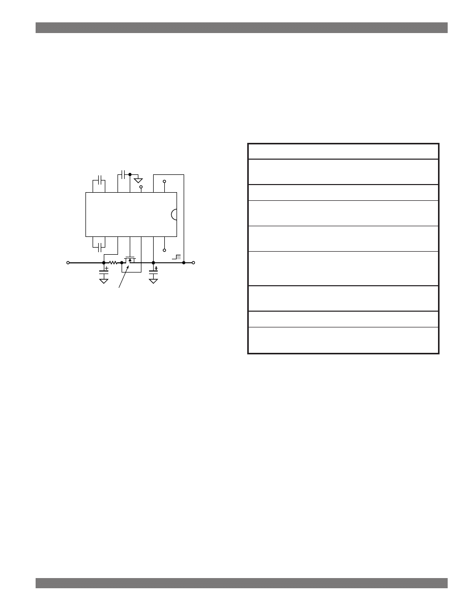
Designing With LDO Regulators
67
Section 4: Linear Regulator Solutions
Micrel Semiconductor
Designing With LDO Regulators
low dropout 3.3V, 10A supply application. Capacitors
C1 and C2 perform the voltage tripling required by
the N-channel logic-level MOSFETs. Improved re-
sponse to load transients is accomplished by using
output capacitors with low ESR characteristics. The
exact capacitance value required for a given design
depends on the maximum output voltage disturbance
that can be tolerated during a worse case load
change. Adding low-value (0.01
µ
F to 0.1
µ
F) film ca-
pacitors (such as Wima MKS2 series) near the load
will also improve the regulator’s transient response.
1
2
3
4
14
13
12
11
5
6
7
10
9
8
MIC5157
C2+
C2–
V
CP
GND
FLAG
3.3V
5V
C1+
C1–
V
DD
G
D
S
EN
V
OUT
+3.3V, 10A
V
IN
(+3.61V min.)
C2
0.1µF
C3 1.0µF
C1
0.1µF
R
S
R
S
= 0.035V / I
LIMIT
3m
Ω
IRLZ44 (Logic Level MOSFET)
*
* Improves transient
response to load changes
Enable
Shutdown
Q1
Figure 4-6. 10A Linear Regulator
Comparison With Monolithics
Similarities to Monolithics
Like Micrel’s Super ßeta PNP monolithic regu-
lators, the Super LDO is a linear regulator. It provides
a regulated and filtered output voltage from a (at least)
slightly higher input source; it does not require induc-
tors; it is available in fixed as well as user-adjustable
output voltages; and it protects itself and its load by
implementing current limiting. There are significant
differences between the Super LDO and monolithic
designs, however.
Differences from Monolithics
The differences between the Super LDO and
monolithic designs is depicted in Table 4-1. The ex-
ternal N-channel MOSFET required by the Super LDO
gives it great flexibility—by simply selecting the MOS-
FET, the designer may choose output current capa-
bility as well as dropout voltage. You may customize
your regulator for your exact needs: the dropout volt-
age is simply V
DO
= I
×
R
DS ON
and the current limit is
adjustable by selecting one resistor. Also, by placing
the hot pass element away from the sensitive refer-
ence and voltage comparators, better performance
over the operating temperature range and much
higher output currents are possible.
The Super LDO does not offer thermal shutdown
protection and the pass MOSFET’s tab is V
OUT
in-
stead of ground, unlike the Super
β
eta PNP versions.
Above approximately 5A, the Super LDO is gen-
erally the most economical regulation solution.
Super LDO
Monolithic LDO
“Any” output current
Output current set by
die size
Adjustable current limit
Fixed Current limit
User-selectable dropout
Dropout voltage set by
voltage
die size
Better stability than
PNP LDOs
Reference temperature
Reference gets hot
independent of hot pass
element
Pass transistor
Tab is grounded
tab is V
OUT
No thermal shutdown
Thermal shutdown
Multiple component
Only capacitors needed
solution
Table 4-1. Super LDO and Monolithic
Regulator Comparison
Unique Super LDO Applications
Super High-Current Regulator
Figure 4-7 shows a linear regulator offering out-
put current to 30A with a dropout voltage of only
330mV. Current limit is set to 45A. With proper cool-
ing and current-limit resistor changes, this circuit
scales to any arbitrary output current: 50A, 100A—
you name it!
Achieving the heat sinking required for the high
current output mentioned above is difficult. As output
current and/or input-to-output voltage differentials in-
crease, the heat sink size rapidly increases. One tech-
nique to ease the heat sinking problem is to split the
heat generators into multiple sources—by using mul-
tiple pass MOSFETs in parallel.
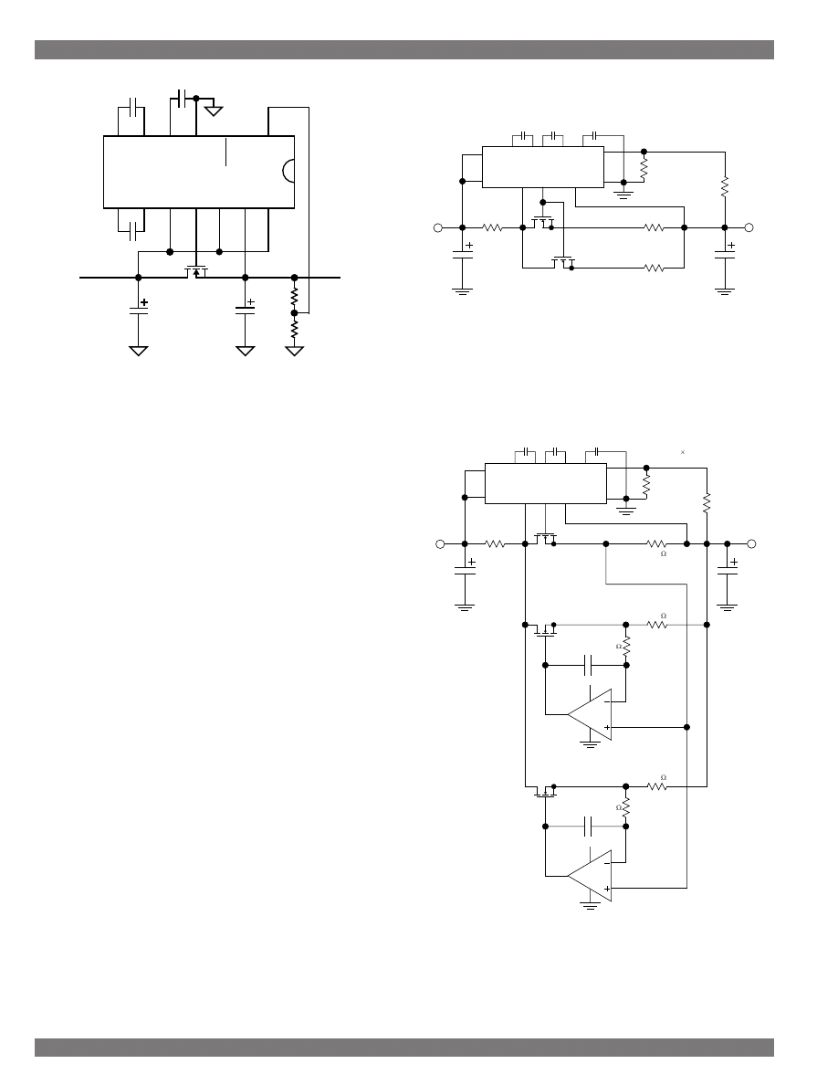
Micrel Semiconductor
Designing With LDO Regulators
Section 4: Linear Regulator Solutions
68
Designing With LDO Regulators
Unlike bipolar transistors, MOSFETs have a
negative temperature coefficient of resistance. This
makes them easier to parallel than bipolars. The
MOSFET carrying more current heats up; the heat
increases the channel resistance, reducing the cur-
rent flow through that FET.
Unfortunately for Super LDO applications, the
MOSFET threshold voltage varies from part-to-part
and over the operating temperature range. Unlike
power switching applications, Super LDO linear regu-
lator operation of the pass MOSFET is in the linear
region, which is at or just above the threshold. This
means device-to-device threshold voltage variation
causes mismatch.
If two MOSFETs are mounted on the same heat
sink, it is possible to directly parallel them in less de-
manding applications where the maximum output
current is within the rating of a single device and total
power dissipation is close to that possible with a single
unit.
A better solution, usable with two or more MOS-
FETs in parallel, is to use ballast resistors in series
with the source lead (output). Size the ballast resis-
tors to drop a voltage equal to or a bit larger than the
worst-case gate-to-source threshold voltage variation.
As current flow through one MOSFET and ballast
resistor increases, the ballast resistor voltage drop
reduces MOSFET V
GS
, increasing its resistance. This
Figure 4-7. A High Current Regulator Using the
MIC5158
reduces current flow through that MOSFET. Figure
4-8 shows an example of this technique.
50m
Ω
680µF
680µF
5V
3.3V
at
20A
MIC158
VIN
EN
EA
GND
VOUT = 1.235
×
(1 + R1/R2)
S
D
G
1m
Ω
R2
11.8k
Ω
R1
19.6k
Ω
Q1
C1+
C1– C2+
C2–
VCP
0.1µF
10µF
0.1µF
+
50m
Ω
Q2
Figure 4-8. Ballast Resistors Promote Current
Sharing With Parallel MOSFETs
Lower dropout voltage and even better match-
ing is possible using op amps to force sharing. A low
current drain op amp may be powered by the V
CP
pin
of the MIC5157 or MIC5158, as shown in Figure 4-9.
10k
3
4
1
5
2
+ VCP
10m
0.01µF
10m
1000µF
6800µF
3.6V
to
6V
3.3V
at
35A
MIC158
VIN
EN
EA
GND
10m
VOUT = 1.235 (1 + R1/R2)
10k
3
4
1
5
2
+ VCP
S
D
G
0.7m
Ω
R2
11.8k
Ω
R1
19.6k
Ω
Q1
Q2
Q3
C1+
C1– C2+
C2–
VCP
0.1µF
10µF
0.1µF
+
Figure 4-9. Parallel MOSFETs for High Current
and/or High Power Dissipation Regulators
1
2
3
4
14
13
12
11
5
6
7
10
9
8
MIC5158
C1+
C1–
V
DD
V
OUT
3.3V, 10A
V
IN
(5V)
C2
0.1µF
C3
3.3µF
C1
0.1µF
C
OUT
47µF
* For V
IN
> 5V, use IRFZ44.
C2+
C2–
GND
G
D
S
V
CP
FLAG
R1
17.8k
Ω
, 1%
R2
10.7k
Ω
, 1%
Q1*
IRLZ44
C
IN
47µF
EN
5V FB
EA
Designing With LDO Regulators
69
Section 4: Linear Regulator Solutions
Micrel Semiconductor
Designing With LDO Regulators
Table 4-2. Copper Wire Resistance
AWG
Wire
Resistance at 20
°
C
Size
10-6
Ω
/ cm
10-6
Ω
/ in
10
32.70
83.06
11
41.37
105.1
12
52.09
132.3
13
65.64
166.7
14
82.80
210.3
15
104.3
264.9
16
131.8
334.8
17
165.8
421.1
18
209.5
532.1
19
263.9
670.3
20
332.3
844.0
21
418.9
1064.0
22
531.4
1349.8
23
666.0
1691.6
24
842.1
2138.9
25
1062.0
2697.5
26
1345.0
3416.3
27
1687.6
4286.5
28
2142.7
5442.5
29
2664.3
6767.3
30
3402.2
8641.6
31
4294.6
10908.3
32
5314.9
13499.8
33
6748.6
17141.4
34
8572.8
21774.9
35
10849
27556.5
36
13608
34564.3
37
16801
42674.5
38
21266
54015.6
39
27775
70548.5
40
35400
89916.0
41
43405
110248.7
42
54429
138249.7
43
70308
178582.3
44
85072
216082.9
Selecting the Current Limit Threshold
By choosing one resistor value, the current limit
threshold of the Super LDO is set. The resistor is cho-
sen to drop 35mV at the desired output current limit
value. While discrete resistors may be used, a more
economical solution is often a length of copper wire
or PC board trace used as the current sense resistor.
The wire diameter or the width of the copper trace
must be suitable for the current density flowing
through it, and its length must provide the required
resistance.
Sense Resistor Power Dissipation
The power dissipation of sense resistors used
in Super LDO regulator circuits is small and gener-
ally does not require the power dissipation capability
found in most low-value resistors.
Kelvin Sensing
A Kelvin, or four-lead, connection is a measure-
ment connection that avoids the error caused by volt-
age drop in the high-current path leads.
Referring to Figure 4-10, sense leads are at-
tached directly across the resistance element—inten-
tionally excluding the power path leads. Because the
sense conductors carry negligible current (sense in-
puts are typically high impedance voltage measure-
ment inputs), there is no voltage drop to skew the
E = I
×
R measurement.
Force +
Sense +
Sense –
Force –
Figure 4-10. A Kelvin-sense Resistor
Manufacturers of Kelvin-sensed resistors are
listed in the References section.
Alternative Current Sense Resistors
A low-value resistor can be made from a length
of copper magnet wire or from a printed circuit board
trace. Tables 4-2, 4-3, and 4-4 are provided for wire
and printed circuit traces.
Copper has a positive temperature coefficient
of resistivity of +0.39%/
°
C. This can be significant
when higher-accuracy current limiting is required.
A Kelvin connection between the sense element
and the Super LDO Regulator Controller improves
the accuracy of the current limit set-point.
Overcurrent Sense Resistors from PC
Board Traces
Building the resistor from printed-circuit board
(PCB) copper is attractive; arbitrary values can be
provided inexpensively. The ever-shrinking world of
electronic assemblies requires minimizing the physi-
cal size of this resistor which presents a power-dissi-
pation issue. Making the resistor too small could
cause excessive heat rise, leading to PCB trace dam-
age or destruction (i.e., a fuse rather than a controlled
resistor).
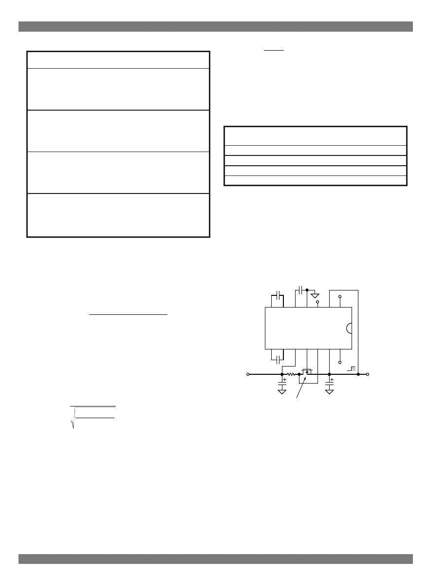
Micrel Semiconductor
Designing With LDO Regulators
Section 4: Linear Regulator Solutions
70
Designing With LDO Regulators
Table 4-3 Printed Circuit Copper Resistance
Conductor
Conductor Width
Resistance
Thickness
(inches)
m
Ω
/ in
0.5oz/ft
2
0.025
39.3
(18
µ
m)
0.050
19.7
0.100
9.83
0.200
4.91
0.500
1.97
1 oz/ft
2
0.025
19.7
(35
µ
m)
0.050
9.83
0.100
4.91
0.200
2.46
0.500
0.98
2oz/ft
2
0.025
9.83
(70
µ
m)
0.050
4.91
0.100
2.46
0.200
1.23
0.500
0.49
3oz/ft2
0.025
6.5
(106
µ
m)
0.050
3.25
0.100
1.63
0.200
0.81
0.500
0.325
Resistor Design Method
Three design equations provide a resistor that
occupies the minimum area. This method considers
current density as it relates to heat dissipation in a
surface layer resistor.
(4-1)
ρ
ρ
α
S
A
RISE
T =
1
T
T
20
h
( )
+
+
−
(
)
[
]
where:
ρ
s
(T) = sheet resistance at elevated temp. (
Ω
/
G
)
ρ
= 0.0172 = copper resistivity at 20
°
C (
Ω
•
µ
m)
α
= 0.00393 = temperature coefficient of
ρ
(per
°
C)
T
A
= ambient temperature (
°
C)
T
RISE
= allowed temperature rise (
°
C)
h = copper trace height (
µ
m, see Table 4-4)
(4-2)
w
1000I
T
T
MAX
RISE
SA
S
=
÷
( )
θ
ρ
where:
w = minimum copper resistor trace width (mils)
I
MAX
= maximum current for allowed T
RISE
(A)
T
RISE
= allowed temperature rise (
°
C)
θ
SA
= resistor thermal resistance (
°
C
×
in
2
/W)
ρ
s
(T) = sheet resistance at elevated temp. (
Ω
/
G
)
Note:
θ
SA
≈
55
°
C • in
2
/W
(4-3)
l
=
( )
w R
T
S
ρ
where:
l
=
resistor length (mils)
w = resistor width (mils)
R = desired resistance (
Ω
)
ρ
s
(T) = sheet resistance at elevated temp. (
Ω
/
G
).
PCB Weight
Copper Trace Height
(oz/ft
2
)
(mils)
(
µ
m)
1/2
0.7
17.8
1
1.4
35.6
2
2.8
71.1
3
4.2
106.7
Table 4-4. Copper Trace Heights
Design Example
Figure 4-11 is a circuit designed to produce a
3.3V, 10A output from a 5V input. Meeting the design
goal of occupying minimal PC board space required
minimizing sense resistor area. This resistor is shown
as R
S
.
1
2
3
4
14
13
12
11
5
6
7
10
9
8
MIC5157
C2+
C2–
V
CP
GND
FLAG
3.3V
5V
C1+
C1–
V
DD
G
D
S
EN
V
OUT
3.3V, 10A
V
IN
(3.6V min.)
0.1µF
1.0µF
0.1µF
R
S
R
S
= 0.035V / I
LIMIT
4m
Ω
IRLZ44 (Logic Level MOSFET)
C
L
*
47µF
* Improves transient
response to load changes
Enable
Shutdown
47µF
Figure 4-11. Regulator Circuit Diagram
The 4m
Ω
current-sensing resistor (R
S
) of Fig-
ure 4-11 is designed as follows: (1) based on copper
trace height and an allowed temperature rise for the
resistor, calculate the sheet resistance using Equa-
tion 4-1; (2) based on the maximum current the re-
sistor will have to sustain, calculate its minimum trace
width using Equation 4-2; and (3) based on the de-
sired resistance, calculate the required trace length
using Equation 4-3.
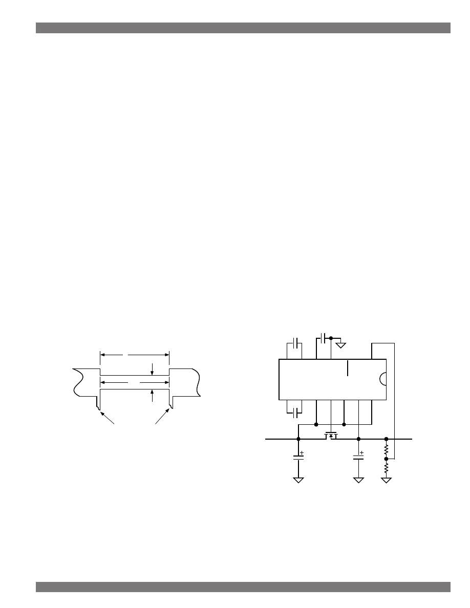
Designing With LDO Regulators
71
Section 4: Linear Regulator Solutions
Micrel Semiconductor
Designing With LDO Regulators
Calculate Sheet Resistance
This design uses 1 oz/ft
2
weight PCB material,
which has a copper thickness (trace height) of
35.6
µ
m. See Table 4-4. Allowing the resistor to pro-
duce a 75
°
C temperature rise will place it at 100
°
C
(worst case) when operating in a 25
°
C ambient envi-
ronment:
ρ
s
(T) = 635
×
10
–6
Ω
= 0.635 m
Ω
/
G
.
Calculate Minimum Trace Width
The design example provides an output current
of 5A. Because of resistor tolerance and the current-
limit trip-point specification of the MIC5158 (0.028 to
0.042V), a trip-point of 8.75A is chosen, allowing for
as much as 10A of current during the sustained limit-
ing condition:
w = 215.8 mils
≈
216 mils.
Calculate Required Trace Length
The length of a 4m
Ω
resistor is determined via
Equation 4-3 as follows:
l
= 1360.6 mils
≈
1361 mils.
Resistor Layout
To avoid errors caused by voltage drops in the
power leads, the resistor should include Kelvin sens-
ing leads. Figure 4-12 illustrates a layout incorporat-
ing Kelvin sensing leads.
w
l
Kelvin Leads
Power
Lead
Power
Lead
R
S
Figure 4-12. Typical Kelvin Resistor Layout
Thermal Considerations
The previous equations produce a resistance of
the desired value at
elevated temperature. It is im-
portant to consider resistance at temperature because
copper has a high temperature coefficient. This de-
sign method is appropriate for current-sensing resis-
tors because their accuracy should be optimized for
the current they are intended to sense.
Resistor Dimensions Spreadsheet
A spreadsheet is available to ease the calcula-
tion process. Its source code, in Lotus 1-2-3 format,
is available via e-mail from Micrel. Send a message
to
apps@micrel.com
requesting “SENSERES.WK1”
Design Aids
Table 4-4 provides an input needed for Equa-
tion 4-1 (trace height), and Figure 3-63 [from Section
3,
Thermal Management] indicates that 1 in
2
(645
mm
2
) of solder-masked copper in still air has a ther-
mal resistance of 55
°
C/W. Different situations; e.g.,
internal layers or plated copper, will have different
thermal resistances. Other references include MIL-
STD-275E:
Printed Wiring for Electronic Equipment.
Highly Accurate Current Limiting
Improving upon the accuracy of the current limit
mechanism is possible. Refer to Section 3 for a de-
scription of using the Super LDO as a highly accu-
rate adjustable current source.
Protecting the Super LDO from Long-
Term Short Circuits
Foldback current limiting is a useful feature for
regulators like the Super LDO that do not have over-
temperature shutdown.
1
2
3
4
14
13
12
11
5
6
7
10
9
8
MIC5158
C1+
C1–
V
DD
V
OUT
3.3V, 10A
V
IN
(5V)
C2
0.1µF
C3
3.3µF
C1
0.1µF
C
OUT
**
47µF
* For V
IN
> 5V, use IRFZ44.
* * Improves transient response to load changes.
C2+
C2–
GND
G
D
S
V
CP
FLAG
R1
17.8k
Ω
, 1%
R2
10.7k
Ω
, 1%
Q1*
IRLZ44
C
IN
47¨µF
EN
5V FB
EA
Figure 4-13. Simple 10A, 5V-to-3.3V,
Voltage Regulator
A momentary short can increase power dissipa-
tion in a MOSFET voltage regulator pass device to a
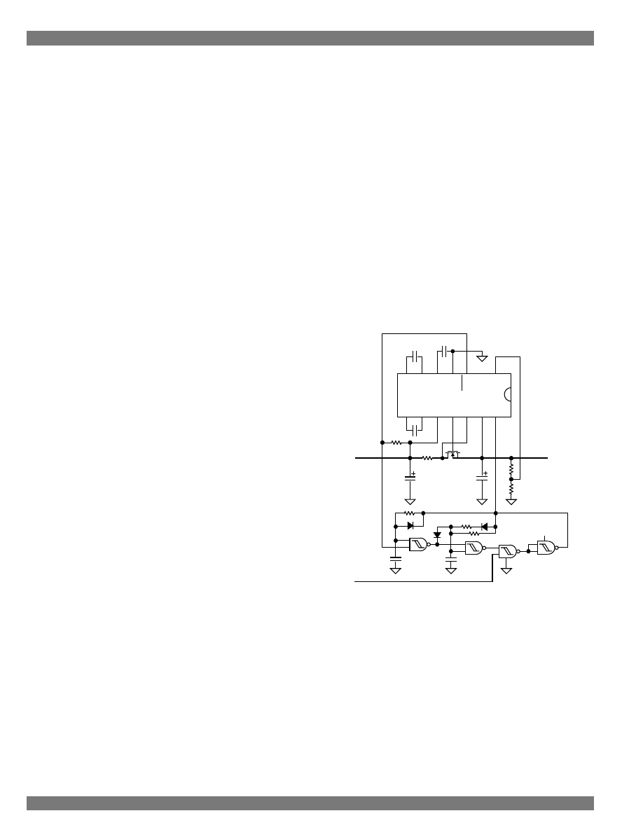
Micrel Semiconductor
Designing With LDO Regulators
Section 4: Linear Regulator Solutions
72
Designing With LDO Regulators
catastrophic level. In the circuit of Figure 4-13, nor-
mal Q1 power dissipation is I
OUT
×
V
DS
, or
(5 – 3.3)V
×
10A = 17W.
Given the 0.028
Ω
R
DS(ON)
of the IRLZ44, if the output
of the power supply is shorted, power dissipation be-
comes (V
IN
/R
DS(ON)
)
2
×
R
DS(ON)
, or an unworkable
892W. Conservative heat sink design will not help
matters!
The Micrel MIC5156/5157/5158 Super LDO™
Regulator Controllers offer two features that can be
used to save the pass device. The first feature is a
current limit capability (not implemented in Figure 4-
13). Output current can be limited at a user-defined
value, but the function is not the classic foldback
scheme. While fixed-value current limiting can reduce
shorted-output power dissipation to a manageable
level, the additional dissipation imposed by the short
can still threaten the pass device. Power dissipation
of a current-limited supply is the full supply voltage
multiplied by the current limit of the regulator system:
5V
×
(>) 10A > 50W. At higher input supply voltages
and/or higher current limit levels, power dissipation
rises rapidly—a 30V supply limited to 10A has a short-
circuit dissipation of 300W. When considerable volt-
age is being dropped by the pass device the short-
circuit power dissipation becomes dramatically high.
The second feature offered by the MIC5156/
5157/5158 is an error flag. This is an open-collector
output which generates a signal if the output voltage
is approximately 6% or more below the intended
value. This flag output is asserted logic low in the
event of a shorted output, and may be used to con-
trol the enable-input pin of the regulator, disabling it
upon detection of a low output voltage condition.
An Example
Figure 4-14 implements both the current-limit ca-
pability and a control scheme for dealing with shorted
outputs. The 2.3m
Ω
resistor R
S
provides for current
limiting at about 15A. Since a shorted output may be
momentary, the circuitry built around U1 automati-
cally restarts the regulator when a short is removed.
Existence of a shorted output is continually monitored;
the system will protect the pass device for an indefi-
nite time. When a short exists the regulator is en-
abled for a very brief interval and disabled for a much
longer interval. Power dissipation is reduced by this
drop in duty cycle, which may be empirically designed.
Circuit Description
Schmitt-trigger NAND-gate A is used to control
a gated oscillator (gate B). Resistors R5 and R6, di-
ode D3, and capacitor C5 provide oscillator timing.
With the values shown the enable time is about 110ms
approximately every 2.25ms. This provides a safe
1:20 ON/OFF ratio (5% duty cycle) for reducing power
dissipated by the pass device. Diode D2 keeps C5
discharged until gate A enables the oscillator. This
assures that oscillation will begin with a full-width short
enable pulse. Different enable and/or disable times
may be appropriate for some applications. Enable
time is approximately k1
×
R5
×
C5; disable time is
approximately k2
×
R6
×
C5. Constants k1 and k2
are determined primarily by the two threshold volt-
ages (V
T
+ and V
T
–) of Schmitt-trigger gate B. Values
for k1 and k2 (empirically derived from a breadboard)
are 0.33 and 0.23, respectively. Component toler-
ances were ignored.
1
2
3
4
14
13
12
11
5
6
7
10
9
8
MIC5158
C1+
C1–
V
DD
V
OUT
3.3V, 10A
V
IN
(5V)
C2
0.1µF
C3
3.3µF
C1
0.1µF
R
S
2.3m
Ω
C
OUT
**
47
µ
F
All Diodes Are 1N914
* For V
IN
> 5V, use IRFZ44.
* * Improves transient response to load changes.
C
IN
47
µ
F
R3 10k
C2+
C2–
GND
G
D
S
V
CP
FLAG
R1
17.8k
Ω
, 1%
R2
10.7k
Ω
, 1%
Q1*
IRLZ44
EN
5V FB
EA
System
Enable
U1
CD4093BC
A
B
C
D
1
2
3
4
5
6
8
9
10
12
13
11
14
V
IN
7
C4
470pF
C5
0.01
µ
F
R4 10k
D1
D2
D3
R5 33k
Ω
R6 1M
R
S
≈
0.035V / I
LIMIT
Figure 4-14. Short-Circuit Protected 10A Regulator
Getting Started
The protection circuitry provides a system en-
able input. Use of this input is optional; it should be
tied to V
IN
if not required. Since the output of gate B
is logic high when the oscillator is disabled, a logic-
high system enable input enables the MIC5158, which
immediately produces a brief logic-low flag output
because initially, the output voltage is too low. Since

Designing With LDO Regulators
73
Section 4: Linear Regulator Solutions
Micrel Semiconductor
Designing With LDO Regulators
the power supply output may or may not be shorted it
is desirable to wait and see. The required wait-delay
timing is implemented by resistor R4, capacitor C4,
and diode D1. The leading-edge of the regulator en-
able signal is delayed (before application to gate A)
for about 4ms, to attempt to span the width of the
logic-low flag that is generated during a normal (non-
shorted) regulator start-up.
Providing enough delay time to span the time of
the flag may not always be practical, especially when
starting with high-capacitance loads. If the logic-low
flag is longer than the delayed enable input to gate A,
the oscillator will cycle through its ON/OFF duty cycle
and the circuit will again attempt a normal start-up.
This will result in a slowing of the regulator turn-on,
but this is not usually objectionable because it reduces
turn-on surge currents.
After start-up, the logic-high inputs to gate A hold
the oscillator off, and the system remains enabled as
long as no error flag is generated. If the flag is gener-
ated due to a short, the MIC5158 remains enabled
only for the time of the oscillator enable pulse and is
then immediately disabled for the duration of the os-
cillator cycle. As long as the short exists, the oscilla-
tor runs and the system monitors the flag to detect
removal of the short. Meanwhile the MOSFET stays
alive, and the system again starts when the short is
removed.

Micrel Semiconductor
Designing With LDO Regulators
Section 5: Data Sheets
74
Designing With LDO Regulators
Data Sheet Reference Section Omitted for This Online Version
http://www.micrel.com

Designing With LDO Regulators
75
Section 6: Packaging
Micrel Semiconductor
Designing With LDO Regulators
Section 6. Package Information
Section 6: Packaging
76
Designing With LDO Regulators
Micrel Semiconductor
Designing With LDO Regulators
Tape & Reel
Surface mount and TO-92 devices are available in tape and
reel packaging. Surface mount components are retained in an
embossed carrier tape by a cover tape. TO-92 device leads
are secured to a backing tape by a cover tape. The tape is
spooled on standard size reels.
Ammo Pack
TO-92 devices are also available in an “ammo pack.” TO-92
devices are secured to a backing tape by a cover tape and are
fanfolded into a box. Ammo packs contain the same quantity,
feed direction, and component orientation as a reel.
To order, specify the complete part number with the suffix “AP”
(
example
†
: MICxxxxx Z AP).
Pricing
Contact the factory for price adder and availability.
Packages Available in Tape & Reel
Part
Package
Quantity
Reel
Carrier Tape
Carrier Tape
Number
†
Description
/ Reel
Diameter
Width
Pitch
MICxxxxx M T&R
2,500
13"
12mm
8mm
2,500
13"
16mm
8mm
16-lead SOIC
2,500
13"
16mm
8mm
MICxxxx WM T&R
16-lead wide SOIC
1,000
13"
16mm
12mm
18-lead wide SOIC
1,000
13"
16mm
12mm
20-lead wide SOIC
1,000
13"
24mm
12mm
24-lead wide SOIC
1,000
13"
24mm
12mm
MICxxxx SM T&R
28-lead SSOP
1,000
13"
16mm
12mm
MICxxxxx V T&R
20-lead PLCC
1,000
13"
16mm
12mm
28-lead PLCC
500
13"
24mm
16mm
44-lead PLCC
500
13"
32mm
24mm
MICxxxxx M4 T&R
3,000
7"
8mm
4mm
MICxxxxx M3 T&R
3,000
7"
8mm
4mm
MICxxxxx M5 T&R
3,000
7"
8mm
4mm
MICxxxxx S T&R
2,500
13"
16mm
12mm
MICxxxxx U T&R
750
13"
24mm
16mm
750
13"
24mm
16mm
MICxxxxx Z T&R
2,000
14
1
⁄
4
"
‡
—
1/2"
* Standards are available from: Electronic Industries Associations, EIA Standards Sales Department, tel: (202) 457-4966
†
xxxxx = base part number + temperature designation. Example: MIC5201BM T&R
‡
Cardboard reel
Typical 13" Reel
for Surface Mount Components
Tape & Reel Standards
Embossed tape and reel packaging conforms to:
•
8mm & 12mm Taping of Surface Mount Components for Automatic Handling, EIA-481-1*
•
16mm and 24mm Embossed Carrier Taping of Surface Mount Components for Automatic Handling, EIA-481-2*
•
32mm, 44mm and 56mm Embossed Carrier Taping of Surface Mount Components for Automatic Handling, EIA-
481-3*
Packaging for Automatic Handling
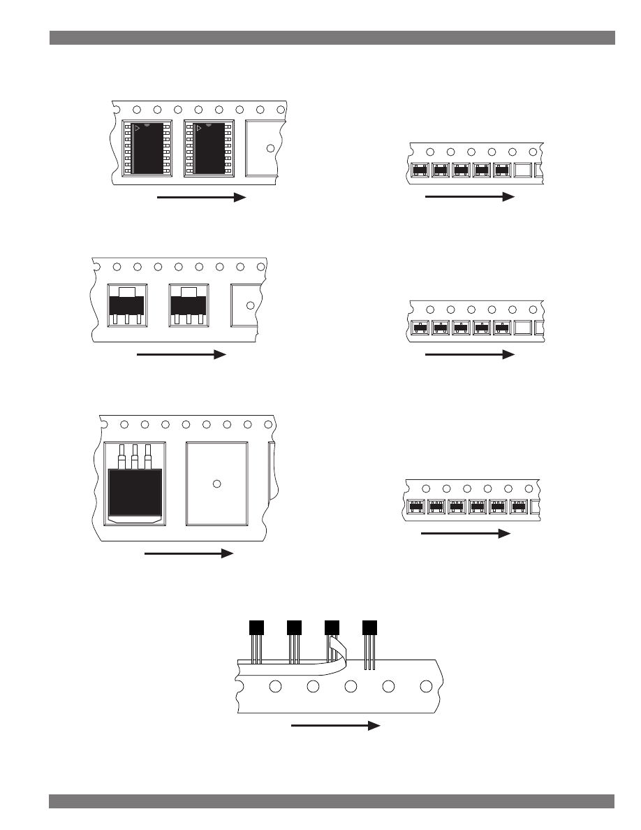
Designing With LDO Regulators
77
Section 6: Packaging
Micrel Semiconductor
Designing With LDO Regulators
Typical SOIC Package Orientation
12mm, 16mm, 24mm Carrier Tape
Feed Direction
Package Orientation
Feed Direction
SOT-143 Package Orientation
8mm Carrier Tape
Feed Direction
SOT-23 Package Orientation
8mm Carrier Tape
Feed Direction
SOT-23-5 Package Orientation
8mm Carrier Tape
SOT-223 Package Orientation
16mm Carrier Tape
Feed Direction
Feed Direction
Typical TO-263 Package Orientation
24mm Carrier Tape
FLAT SURFACE
TOWARD HUB
(DOWN)
Feed Direction
Typical TO-92 Package Orientation
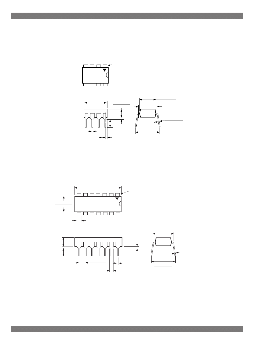
Section 6: Packaging
78
Designing With LDO Regulators
Micrel Semiconductor
Designing With LDO Regulators
14-Pin Plastic DIP (N)
.080 (1.524)
.015 (0.381)
.023 (.5842)
.015 (.3810)
.310 (7.874)
.280 (7.112)
.770 (19.558) MAX
.235 (5.969)
.215 (5.461)
.060 (1.524)
.045 (1.143)
.160 MAX
(4.064)
.160 (4.064)
.100 (2.540)
.110 (2.794)
.090 (2.296)
.400 (10.180)
.330 (8.362)
.015 (0.381)
.008 (0.2032)
.060 (1.524)
.045 (1.143)
PIN 1
8-Pin Plastic DIP (N)
0.380 (9.65)
0.370 (9.40)
0.135 (3.43)
0.125 (3.18)
PIN 1
DIMENSIONS:
INCH (MM)
0.018 (0.57)
0.100 (2.54)
0.013 (0.330)
0.010 (0.254)
0.300 (7.62)
0.255 (6.48)
0.245 (6.22)
0.380 (9.65)
0.320 (8.13)
0.0375 (0.952)
0.130 (3.30)
Note:
Pin 1 is denoted by one or more of the following: a notch, a printed triangle, or a mold mark.
Linear Regulator Packages
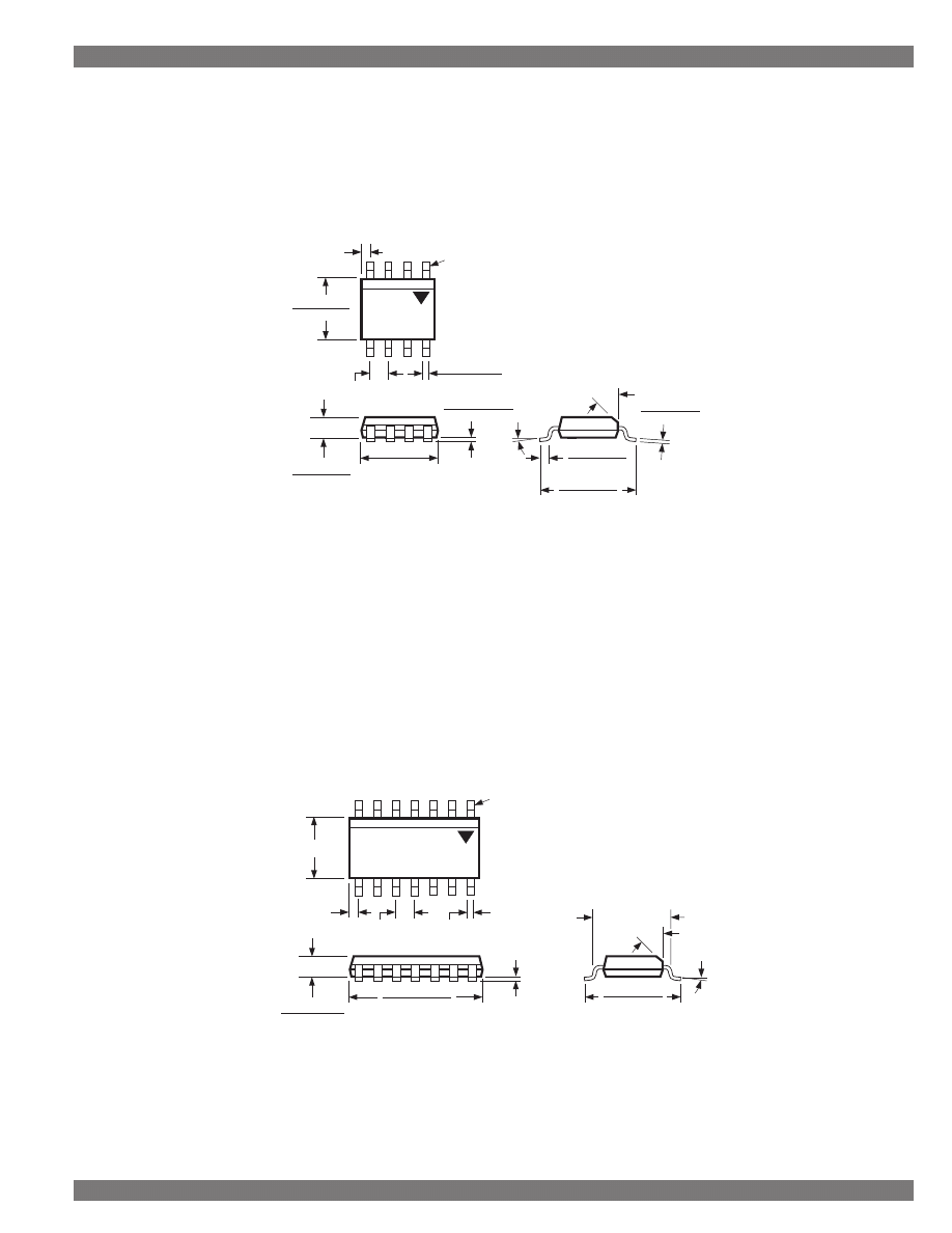
Designing With LDO Regulators
79
Section 6: Packaging
Micrel Semiconductor
Designing With LDO Regulators
8-Pin SOIC (M)
45
°
0
°
–8
°
0.244 (6.20)
0.228 (5.79)
0.197 (5.0)
0.189 (4.8)
SEATING
PLANE
0.026 (0.65)
MAX
)
0.010 (0.25)
0.007 (0.18)
0.064 (1.63)
0.045 (1.14)
0.0098 (0.249)
0.0040 (0.102)
0.020 (0.51)
0.013 (0.33)
0.157 (3.99)
0.150 (3.81)
0.050 (1.27)
TYP
PIN 1
DIMENSIONS:
INCHES (MM)
0.050 (1.27)
0.016 (0.40)
Note:
Pin 1 is denoted by one or more of the following: a notch, a printed triangle, or a mold mark.
14-Pin SOIC (M)
45
°
3
°
–6
°
0.244 (6.20)
0.228 (5.80)
0.344 (8.75)
0.337 (8.55)
0.006 (0.15)
SEATING
PLANE
0.026 (0.65)
MAX
)
0.016 (0.40)
TYP
0.154 (3.90)
0.057 (1.45)
0.049 (1.25)
0.193 (4.90)
0.050 (1.27)
TYP
PIN 1
DIMENSIONS:
INCHES (MM)
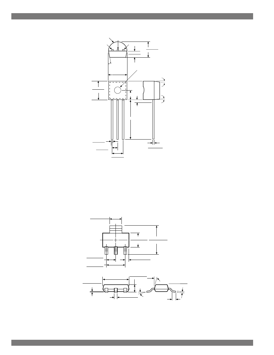
Section 6: Packaging
80
Designing With LDO Regulators
Micrel Semiconductor
Designing With LDO Regulators
TO-92 (Z)
3
2
1
10
°
typ.
5
°
typ.
5
°
typ.
0.185 (4.699)
0.175 (4.445)
0.185 (4.699)
0.175 (4.445)
0.085 (2.159) Diam.
0.500 (12.70) Min.
0.090 (2.286) typ.
0.0155 (0.3937)
0.0145 (0.3683)
Seating Plane
0.025 (0.635) Max
Uncontrolled
Lead Diameter
0.016 (0.406)
0.014 (0.356)
0.105 (2.667)
0.095 (2.413)
0.055 (1.397)
0.045 (1.143)
0.090 (2.286) Radius, typ.
0.145 (3.683)
0.135 (3.429)
0.055 (1.397)
0.045 (1.143)
BOTTOM VIEW
SOT-223 (S)
16
°
10
°
0.84 (0.033)
0.64 (0.025)
1.04 (0.041)
0.85 (0.033)
2.41 (0.095)
2.21 (0.087)
4.7 (0.185)
4.5 (0.177)
6.70 (0.264)
6.30 (0.248)
7.49 (0.295)
6.71 (0.264)
3.71 (0.146)
3.30 (0.130)
3.15 (0.124)
2.90 (0.114)
10
°
MAX
0.10 (0.004)
0.02 (0.0008)
0.038 (0.015)
0.25 (0.010)
C
L
DIMENSIONS:
MM (INCH)
C
L
1.70 (0.067)
1.52 (0.060)
0.91 (0.036) MIN
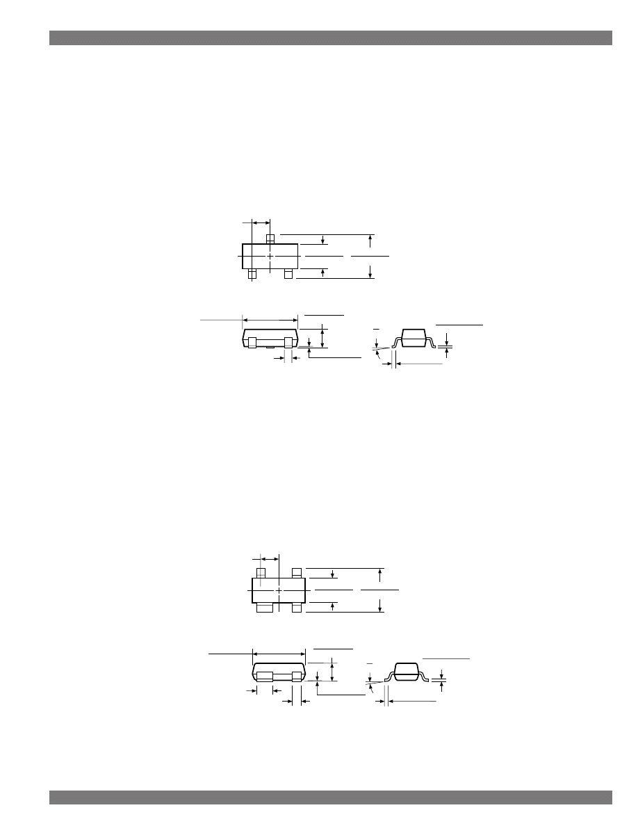
Designing With LDO Regulators
81
Section 6: Packaging
Micrel Semiconductor
Designing With LDO Regulators
SOT-23 (M3)
0.15 (0.006)
0.076 (0.0030)
0.41 (0.016)
0.13 (0.005)
3.05 (0.120)
2.67 (0.105)
8
°
0
°
0.400 (0.0157) TYP 3 PLACES
2.50 (0.098)
2.10 (0.083)
1.40 (0.055)
1.19 (0.047)
0.10 (0.004)
0.013 (0.0005)
1.12 (0.044)
0.76 (0.030)
DIMENSIONS:
MM (INCH)
C
L
0.950 (0.0374) TYP
C
L
SOT-143 (M4)
0.150 (0.0059)
0.089 (0.0035)
8
°
0
°
0.400 (0.016) TYP 3 PLACES
2.50 (0.098)
2.10 (0.083)
1.40 (0.055)
1.20 (0.047)
0.950 (0.0374) TYP
3.05 (0.120)
2.67 (0.105)
0.800 (0.031) TYP
1.12 (0.044)
0.81 (0.032)
0.10 (0.004)
0.013 (0.0005)
DIMENSIONS:
MM (INCH)
0.41 (0.016)
0.13 (0.005)
CL
CL
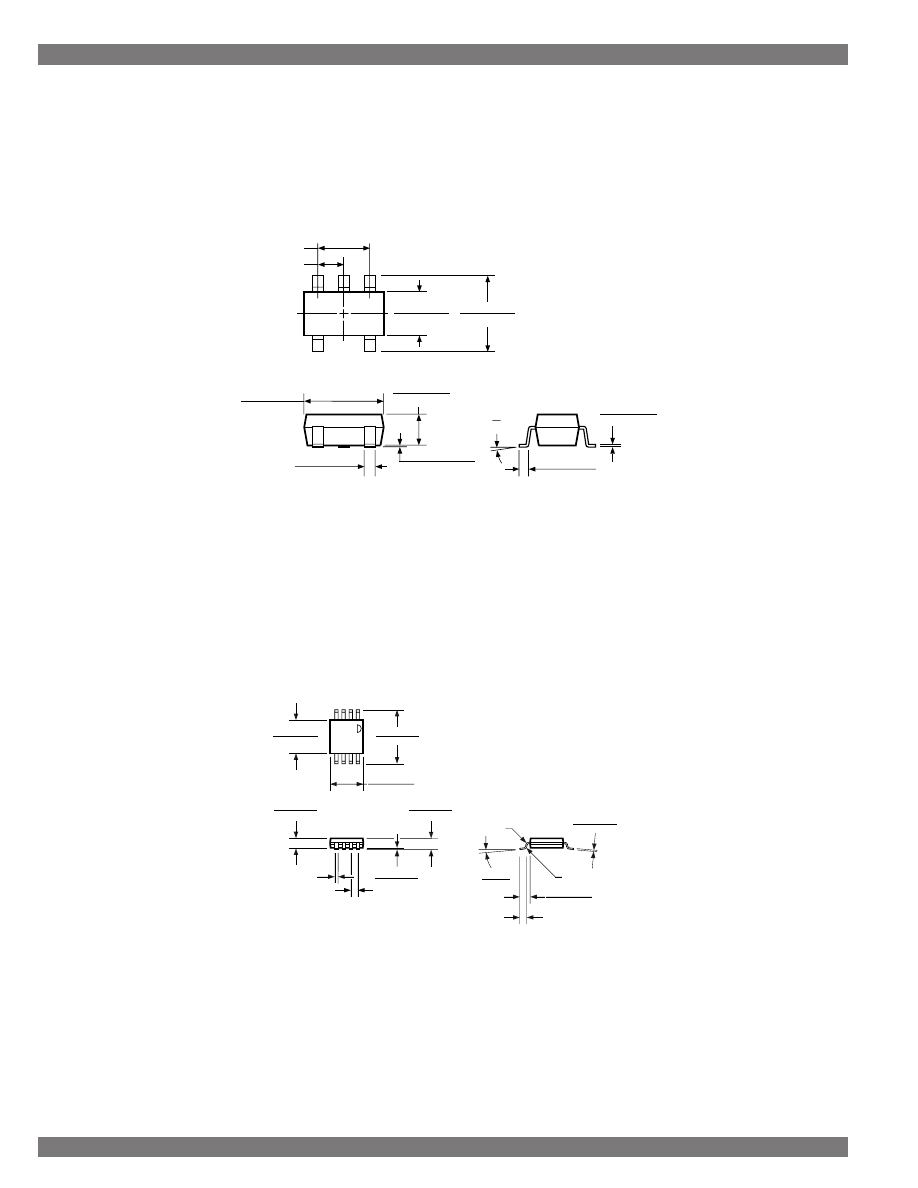
Section 6: Packaging
82
Designing With LDO Regulators
Micrel Semiconductor
Designing With LDO Regulators
SOT-23-5 (M5)
0.20 (0.008)
0.09 (0.004)
0.60 (0.024)
0.10 (0.004)
3.02 (0.119)
2.80 (0.110)
10
°
0
°
3.00 (0.118)
2.60 (0.102)
1.75 (0.069)
1.50 (0.059)
0.95 (0.037) REF
1.30 (0.051)
0.90 (0.035)
0.15 (0.006)
0.00 (0.000)
DIMENSIONS:
MM (INCH)
0.50 (0.020)
0.35 (0.014)
1.90 (0.075) REF
MSOP-8 [MM8™] (MM)
0.008 (0.20)
0.004 (0.10)
0.039 (0.99)
0.035 (0.89)
0.021 (0.53)
0.012 (0.03) R
0.0256 (0.65) TYP
0.012 (0.30) R
5
°
MAX
0
°
MIN
0.122 (3.10)
0.112 (2.84)
0.120 (3.05)
0.116 (2.95)
0.012 (0.03)
0.007 (0.18)
0.005 (0.13)
0.043 (1.09)
0.038 (0.97)
0.036 (0.90)
0.032 (0.81)
DIMENSIONS:
INCH (MM)
0.199 (5.05)
0.187 (4.74)
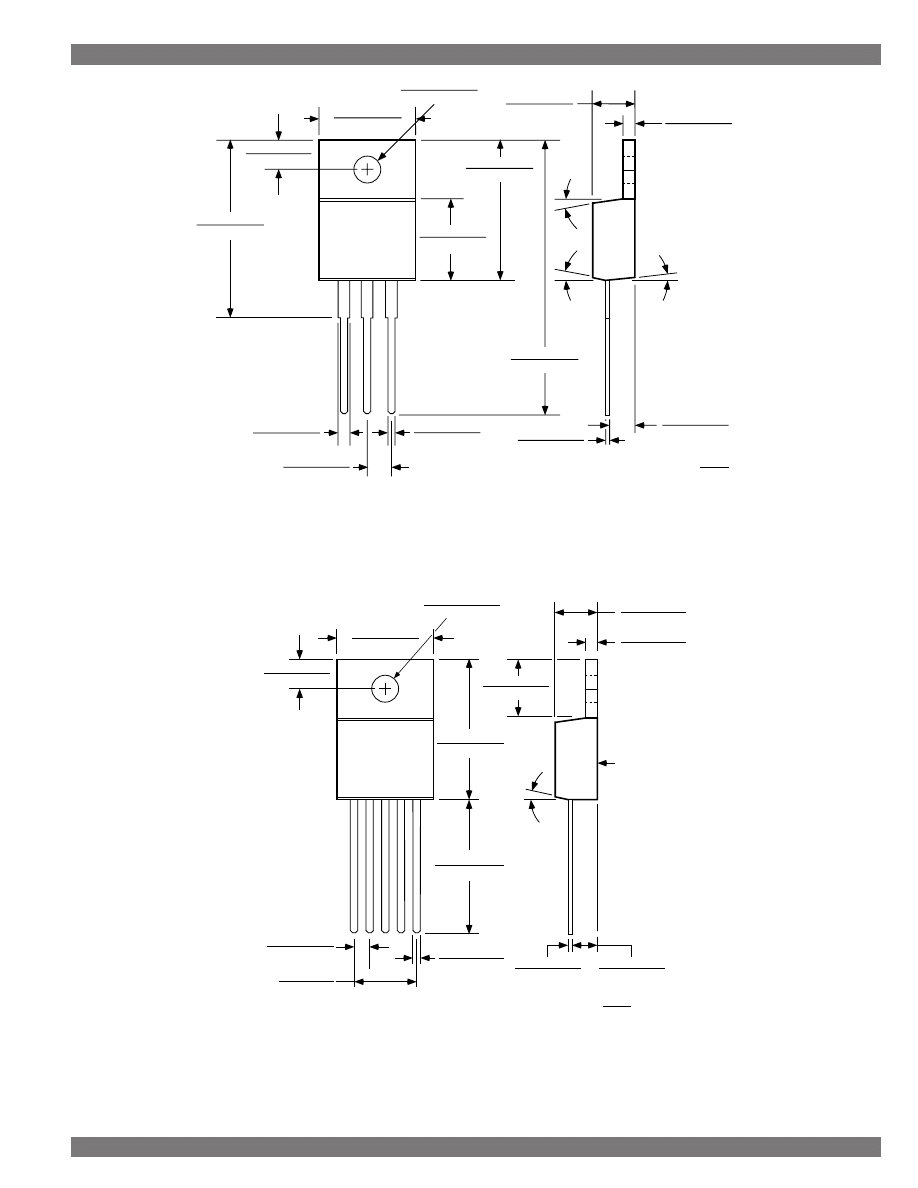
Designing With LDO Regulators
83
Section 6: Packaging
Micrel Semiconductor
Designing With LDO Regulators
5-Lead TO-220 (T)
3-Lead TO-220 (T)
0.015
±
0.003
(0.38
±
0.08)
0.100
±
0.005
(2.54
±
0.13)
0.030
±
0.003
(0.76
±
0.08)
0.050
±
0.003
(1.27
±
.08)
7
°
1.140
±
0.010
(28.96
±
0.25)
0.356
±
0.005
(9.04
±
0.13)
0.590
±
0.005
(14.99
±
0.13)
0.108
±
0.005
(2.74
±
0.13)
0.050
±
0.005
(1.27
±
0.13)
0.151 D
±
0.005
(3.84 D
±
0.13)
0.410
±
0.010
(10.41
±
0.25)
0.176
±
0.005
(4.47
±
0.13)
0.100
±
0.020
(2.54
±
0.51)
0.818
±
0.005
(20.78
±
0.13)
7
°
3
°
DIMENSIONS: INCH
(MM)
0.018
±
0.008
(0.46
±
0.20)
0.268 REF
(6.81 REF)
0.032
±
0.005
(0.81
±
0.13)
0.550
±
0.010
(13.97
±
0.25)
7
°
Typ.
SEATING
PLANE
0.578
±
0.018
(14.68
±
0.46)
0.108
±
0.005
(2.74
±
0.13)
0.050
±
0.005
(1.27
±
0.13)
0.150 D
±
0.005
(3.81 D
±
0.13)
0.400
±
0.015
(10.16
±
0.38)
0.177
±
0.008
(4.50
±
0.20)
0.103
±
0.013
(2.62
±
0.33)
0.241
±
0.017
(6.12
±
0.43)
0.067
±
0.005
(1.70
±
0.127)
inch
(mm)
Dimensions:
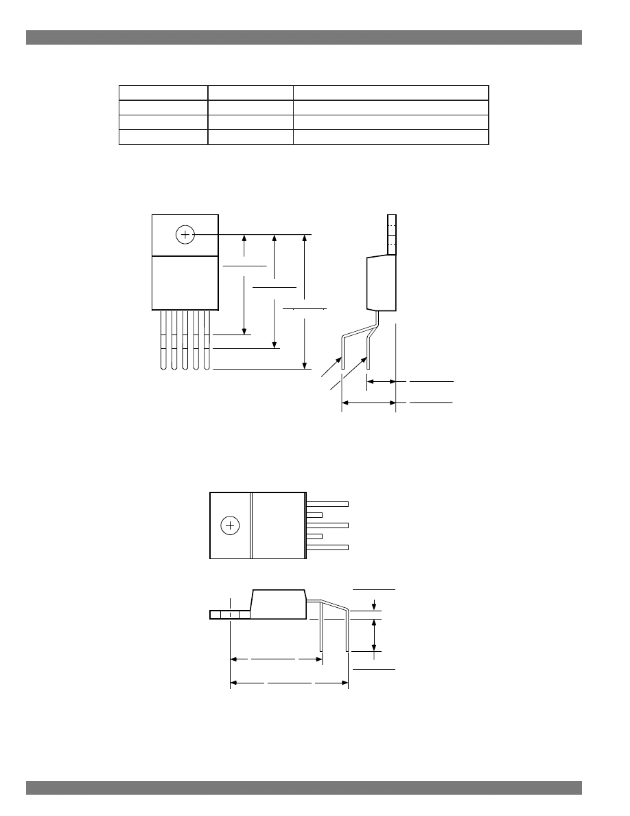
Section 6: Packaging
84
Designing With LDO Regulators
Micrel Semiconductor
Designing With LDO Regulators
0.573
±
0.010
(14.55
±
0.25)
0.735
±
0.010
(18.67
±
0.25)
0.045
±
0.035
(1.14
±
0.89)
0.200
±
0.015
(5.08
±
0.38)
5-Lead TO-220 Horizontal Lead Bend Option (-LB02)
5-Lead TO-220 Vertical Lead Bend Option (-LB03)
0.838
±
0.015
(21.29
±
0.38)
0.704
±
0.015
(17.88
±
0.25)
0.622
±
0.010
(15.80
±
0.25)
0.176
±
0.009
(4.47
±
0.023)
0.334
±
0.010
(8.48
±
0.25)
1
2 3 4 5
Leads 1, 3, 5
Leads 2, 4
Note 1.
Lead protrusion through printed circuit board subject to change.
Note 2.
Lead ends may be curved or square.
Note 1
TO-220 Lead Bend Options
Contact Factory for Availability
Part Number
Package
Lead Form
MICxxxxyT
5-lead TO-220
none (straight)
MICxxxxyT-LB03
5-lead TO-220
vertical, staggered leads, 0.704" seating
MICxxxxyT-LB02
5-lead TO-220
horizontal, staggered leads
MICxxxx = base part number, y = temperature range, T = TO-220
* Leads not trimmed after bending.
Note 2
Note 1
Note 2
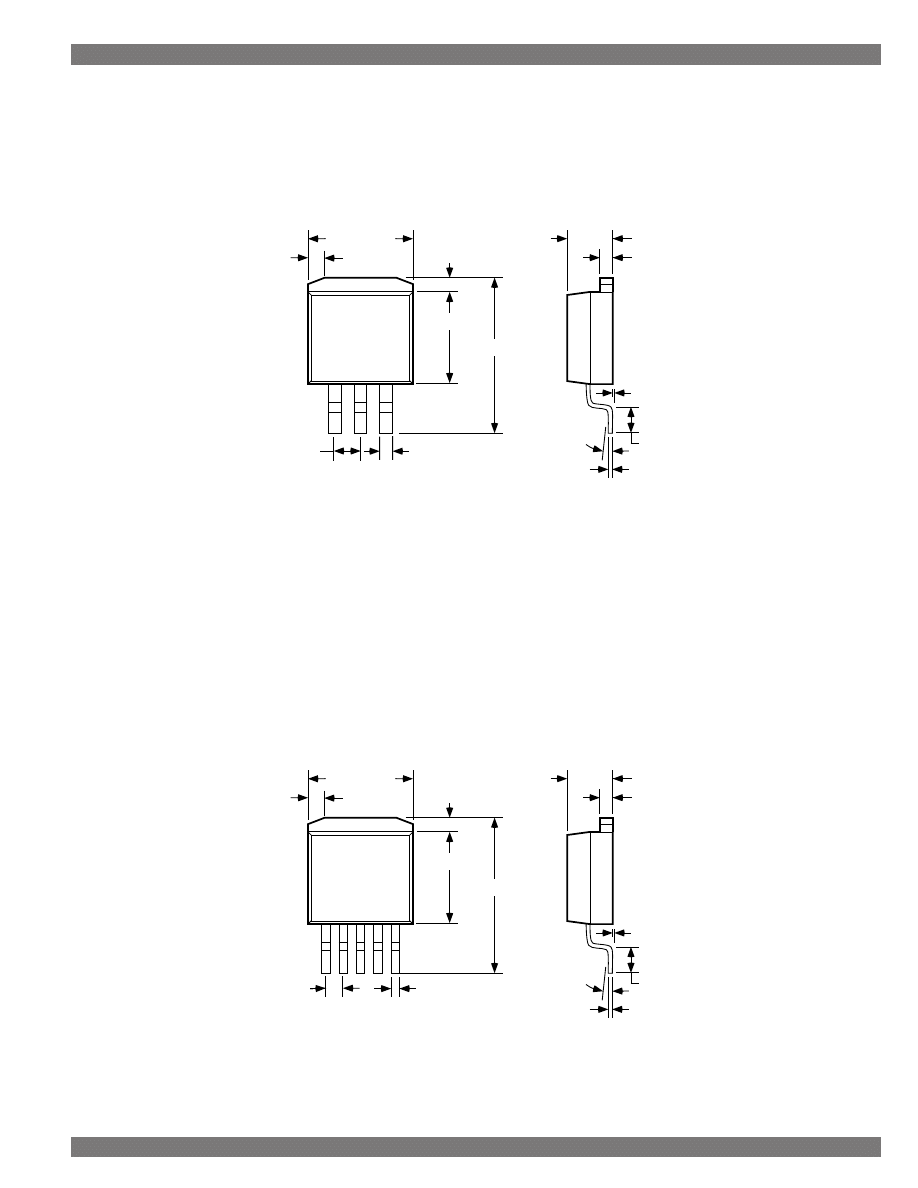
Designing With LDO Regulators
85
Section 6: Packaging
Micrel Semiconductor
Designing With LDO Regulators
5-Lead TO-263 (U)
3-Lead TO-263 (U)
0.067
±
0.005
0.032
±
0.003
0.360
±
0.005
0.600
±
0.025
0.405
±
0.005
0.060
±
0.005
0.176
±
0.005
8
°
MAX
0.100
±
0.01
0.050
±
0.005
0.015
±
0.002
0.004+0.004
–0.008
SEATING PLANE
0.065
±
0.010
20
°±
2
°
DIM. = INCH
0.360
±
0.005
0.600
±
0.025
0.405
±
0.005
0.100 BSC
0.050
0.050
±
0.005
0.176
±
0.005
8
°
MAX
0.100
±
0.01
0.050
±
0.005
0.015
±
0.002
0.004+0.004
–0.008
SEATING PLANE
0.065
±
0.010
20
°±
2
°
DIM. = INCH
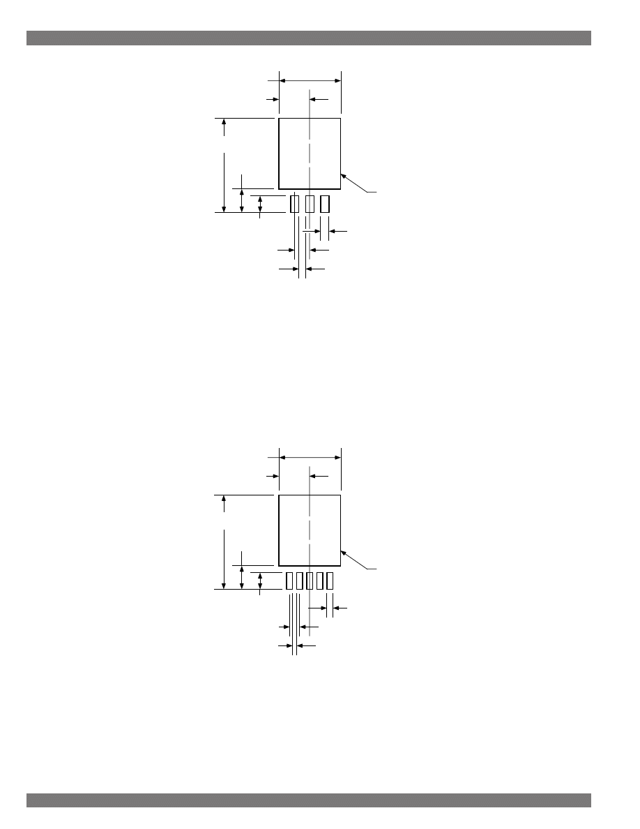
Section 6: Packaging
86
Designing With LDO Regulators
Micrel Semiconductor
Designing With LDO Regulators
Typical 5-Lead TO-263 PCB Layout
Typical 3-Lead TO-263 PCB Layout
0.205
0.410
0.155
NOTE 2
0.625
NOTE 1: PAD AREA MAY VARY WITH
HEAT SINK REQUIREMENTS
NOTE 2: MAINTAIN THIS DIMENSION
NOTE 3: AIR GAP (REFERENCE ONLY)
NOTE 1
DIMENSIONS:
INCHES
0.110 PAD
0.040 PAD
0.067 PITCH
0.022 REF NOTE 3
0.205
0.410
0.110 PAD
0.155
NOTE 2
0.625
0.100 PITCH
0.045 REF NOTE 3
0.055 PAD
NOTE 1: PAD AREA MAY VARY WITH
HEAT SINK REQUIREMENTS
NOTE 2: MAINTAIN THIS DIMENSION
NOTE 3: AIR GAP (REFERENCE ONLY)
NOTE 1
DIMENSIONS:
INCHES
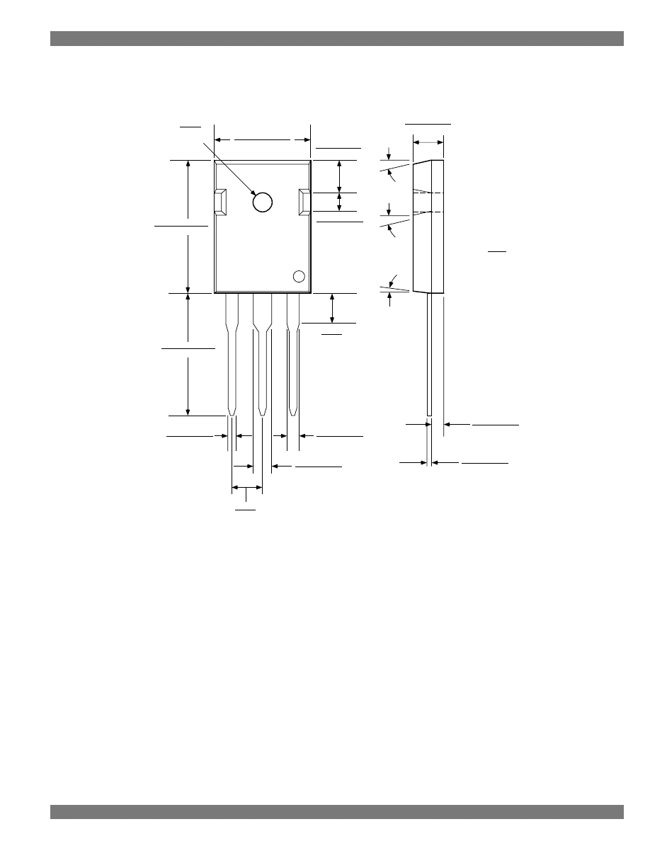
Designing With LDO Regulators
87
Section 6: Packaging
Micrel Semiconductor
Designing With LDO Regulators
3-Lead TO-247 (WT)
0.040 – 0.060
(1.016 – 1.524)
0.780 – 0.820
(19.812 – 20.828)
0.860 – 0.880
(21.844 – 22.352)
0.200
(5.080)
BSC
0.110 – 0.130
(2.794 – 3.302)
0.070 – 0.090
(1.778 – 2.286)
0.250
(6.350)
MAX
MOUNTING HOLE
0.125
(3.175)
DIA TYP
0.620 – 0.640
(15.748 – 16.256)
0.160 – 0.180
(4.064 – 4.572)
0.180 – 0.200
(4.572 – 5.080)
0.190 – 0.210
(4.826 – 5.334)
0.070 – 0.090
(1.778 – 2.286)
0.025 – 0.035
(0.635 – 0.889)
7
°
TYP
15
°
TYP
15
°
TYP
inch
(mm)
Dimensions:
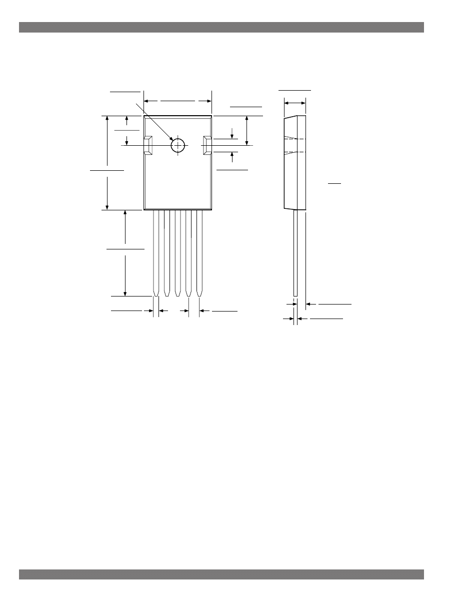
Section 6: Packaging
88
Designing With LDO Regulators
Micrel Semiconductor
Designing With LDO Regulators
5-Lead TO-247 (WT)
0.040 – 0.055
(1.02 – 1.40)
0.780 – 0.800
(19.81 – 20.32)
0.819 – 0.844
(20.80 – 21.44)
0.100 BSC
(2.54 BSC)
MOUNTING HOLE
0.140 – 0.143
(3.56 – 3.63)
DIA TYP
0.620 – 0.640
(15.75 – 16.26)
0.170 – 0.216
(4.32 – 5.49)
0.180 – 0.200
(4.57 – 5.08)
0.185 – 0.208
(4.70 – 5.28)
0.080 – 0.100
(2.03 – 2.54)
0.016 – 0.031
(0.41 – 0.79)
0.242 BSC
(6.15 BSC)
inch
(mm)
Dimensions:

Designing With LDO Regulators
89
Appendices
Micrel Semiconductor
Designing With LDO Regulators
Section 7. Appendices
List of Appendices
Appendix A. Table of Standard 1% Resistor Values ...................................................... 90
Appendix B. Table of Standard
Micrel Semiconductor
Designing With LDO Regulators
Appendices
90
Designing With LDO Regulators
464
475
487
499
511
523
536
549
562
576
590
604
619
634
649
665
681
698
715
732
750
768
787
806
825
845
866
887
909
931
953
976
100
102
105
107
110
113
115
118
121
124
127
130
133
137
140
143
147
150
154
158
162
165
169
174
178
182
187
191
196
200
205
210
215
221
226
232
237
243
249
255
261
267
274
280
287
294
301
309
316
324
332
340
348
357
365
374
383
392
402
412
422
432
442
453
Appendix A. Table of Standard 1% Resistor Values
This table shows three significant digits for standard
±
1% resistor values. These significant digits are
multiplied by powers of 10 to determine resistor values. For example, standard resistor values are 0.100
Ω
,
1.00
Ω
, 1.00k
Ω
, 1.00M
Ω
, 100M
Ω
, etc.
Designing With LDO Regulators
91
Appendices
Micrel Semiconductor
Designing With LDO Regulators
Appendix B. Table of Standard
±
5% and
±
10% Resistor Values
(
±
10% values in bold)
This table shows two significant digits for the standard
±
5% and
±
10% resistor values. These significant
digits are multiplied by powers of 10 to determine resistor values. For example, standard resistor values are
0.1
Ω
, 1.0
Ω
, 1.0k
Ω
, 1.0M
Ω
, 10M
Ω
, etc.
10
11
12
13
15
16
18
20
22
24
27
30
33
36
39
43
47
51
56
62
68
75
82
91
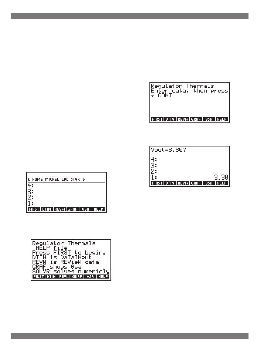
Micrel Semiconductor
Designing With LDO Regulators
Appendices
92
Designing With LDO Regulators
Appendix C. LDO SINK for the HP 48 Calculator
Let’s run the program. Press
FIRST
to begin.
Your screen shows:
After a brief pause, the output voltage prompt
appears:
Enter a new number and press
←
CONT
to con-
tinue. If the data previously entered is still correct,
you may simply press
←
CONT
to retain it. Proceed
through the list, entering data as prompted and press-
ing
←
CONT
to continue. You will be prompted for
Vout
the desired regulator output voltage
Iout
regulator output current
Vmax
the maximum input voltage
Vmin
the lowest input voltage (used only by the
graphing routine
θ
jc
thermal resistance, junction to case
(from the device data sheet)
θ
cs
thermal resistance from the case to the
heat sink
After these data are entered, the Review screen
appears and confirms your entries.
The following program, written for the HP 48 cal-
culator, will calculate all power dissipation and heat
sink related parameters and ease your design opti-
mization process. It will also graph the resulting heat
sink characteristics versus input voltage. The program
listing follows the user information. It was written on a
HP 48S and runs on both the “S” and the 48G(X)
version of the calculator. If you would like to receive
the program electronically, send e-mail to Micrel at
apps@micrel.com
and request program “LDO SINK
for the HP48”. It will be sent via return e-mail.
Using LDO SINK
After loading the program, change to the direc-
tory containing it. In the example shown, it is loaded
into
{HOME MICREL LDO SINK}
.
The first screen you will see looks like this:
Pressing the white
HELP
function key displays
a screen of on-line help.
Pressing either
FIRST
or
DTIN
will start the
program and prompt you for the most commonly
changed data.
REVW
brings up a list of data already
entered.
GRAF
draws the heat sink
θ
SA
versus input
voltage.
SOLVR
begins the built-in solve routine that
allows you to solve for any variable numerically.
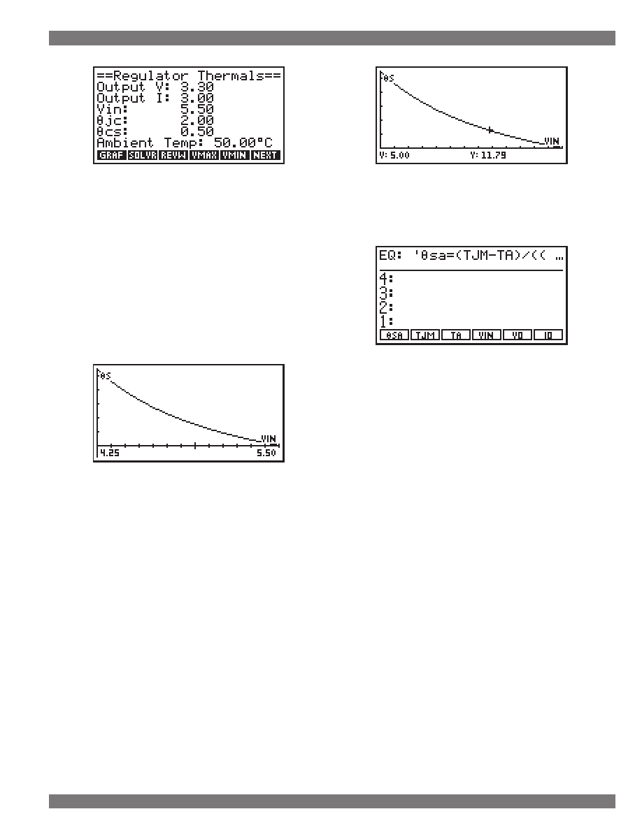
Designing With LDO Regulators
93
Appendices
Micrel Semiconductor
Designing With LDO Regulators
Ambient temperature was not on the list of
prompted data. If you wish to change it, press
ON
(
CANCEL
) followed by the white
NEXT
key. Enter the
ambient temperature followed by the white
TA
key.
Press the white
NEXT
key twice to get to the calcula-
tion menu. Another variable used but not prompted
for is
TJM
, the maximum junction temperature for the
regulator.
You may now press
GRAF
to calculate and view
the
θ
sa
versus
Vin
graph, or
SOLVR
to start the
numerical solve routine. If we press
GRAF
, the follow-
ing is displayed:
This shows the thermal resistance of the heat
sink as the input voltage varies from a low of 4.25V
to a high of 5.50V. Pressing
ON/CANCEL
at this time
returns you to the stack display, with
θ
sa
at the maxi-
mum input voltage displayed.
NOTE: the x-axis is shown beneath the HP 48
graph menu. Press the minus (–) key to toggle be-
tween the menu and axis display. Pressing
TRACE
followed by
(X,Y)
puts the HP 48 in trace mode
and displays the coordinate values of the plot. Press
the cursor keys to move around the plot and show
voltage (
V
) versus
θ
sa
and displays the coordinate
values of the plot. Press the cursor keys to move
around the plot and show voltage (
V
) versus
θ
sa
(y-
axis). Here the cursor has been moved to a
Vin
of
5.00V and shows a required maximum
θ
sa
of 11.79
C/W.
Pressing
ON/CANCEL
returns you to the calcu-
lation menu. If you hit the white
SOLVR
key, the HP
48 Solve application is started and you may solve for
any of the variables numerically.
Enter a value and press its white function key to
modify variables. Use the HP 48
NXT
key to access
θ
jc
and
θ
cs
. Solve for a variable by pressing the
←
key followed by the variable’s white function key.
Press
→
VIEW
(HP 48G) or
←
REVIEW
(HP 48S) to
review all variable values.
Program Listing
For those without the HP 48 compatible serial
cable or e-mail access, here is the program listing for
LDO SINK. “SINK” is installed as a directory. It is
1948.5 bytes long and has a checksum of # 35166d.
%%HP: T(1)A(D)F(.);
DIR
FIRST
« DTIN
»
DTIN
« CLLCD
“Regulator Thermals
Enter data, then press
←
CONT”
1 DISP 3 WAIT CLEAR
VO “Vout=” VO + “?”
+ PROMPT ‘VO’ STO
CLEAR IO “Iout=” IO
+ “?” + PROMPT ‘IO’

Micrel Semiconductor
Designing With LDO Regulators
Appendices
94
Designing With LDO Regulators
STO CLEAR VMAX
“Vmax=” VMAX + “?”
+ PROMPT ‘VMAX’ STO
CLEAR VMIN “Vmin=”
VMIN + “?” + PROMPT
‘VMIN’ STO CLEAR
θ
JC “
θ
jc=”
θ
JC +
“?” + PROMPT ‘
θ
JC’
STO CLEAR
θ
CS
“
θ
cs=”
θ
CS + “?” +
PROMPT ‘
θ
CS’ STO
REVW
»
REVW
« CLLCD
“==Regulator Thermals==”
1 DISP “Output V: “
VO + 2 DISP
“Output I: “ IO + 3
DISP “Vin: “
VMAX VMAX ‘VIN’ STO
+ 4 DISP
“Ambient Temp: “ TA
+ “
°
C” + 7 DISP
“
θ
jc: “
θ
JC +
5 DISP “
θ
cs: “
θ
CS + 6 DISP NEX1
TMENU 3 FREEZE
»
GRAF
« CLLCD
“Regulator Thermals
Graphing
θ
sa vs Vin”
2 FIX 1 DISP ‘(TJM-
TA)/((1.02*VIN-VO)*
IO)-
θ
JC-
θ
CS’ STEQ
FUNCTION ‘VIN’
INDEP VMIN VMAX
XRNG VMIN VMAX
‘VIN’ STO EQ EVAL
R+C AXES { “Vin”
“
θ
S” } AXES AUTO
ERASE DRAW DRAX
LABEL VMAX ‘VIN’
STO EQ EVAL 1 TRNC
“
θ
sa(min)”
→
TAG
PICTURE
»
θ
sa 1.19549150037
HELP
« CLLCD
“Regulator Thermals
HELP file
Press FIRST to begin.
DTIN is DaTaINput
REVW is REVieW data
GRAF shows
θ
sa
SOLVR solves numericly”
1 DISP 3 FREEZE
»
NEX1 { GRAF {
“SOLVR”
« HS STEQ 30
MENU
» } REVW VMAX
VMIN { “NEXT”
« NEX2 TMENU
» } }
NEX2 { VO IO VIN
TA TJM { “NEXT”
« NEX3 TMENU
» } }
NEX3 {
θ
JC
θ
CS “”
“” HELP { “NEXT”
« NEX1 TMENU
» } }
Variables
θ
JC 2
VMAX 5.5
VMIN 4.25
HS ‘
θ
sa=(TJM-TA)/
((1.02*VIN-VO)*IO)-
θ
JC-
θ
CS’
PPAR {
(4.25,6.47110814478)
(5.5,22.6889168766)
VIN 0 {
(4.25,8.5864745011)
“Vin” “
θ
S” }
FUNCTION Y }
EQ ‘
θ
sa=(TJM-TA)/
((1.02*VIN-VO)*IO)-
θ
JC-
θ
CS’
θ
CS .5
IO 6
VO 3.3
VIN 5.5
TJM 125
TA 75
END
Designing With LDO Regulators
95
Appendices
Micrel Semiconductor
Designing With LDO Regulators
Section 8. Low-Dropout Voltage Regulator
Glossary
Dropout (Voltage)
The minimum value of input-to-output voltage differential required
by the regulator. Usually defined as the minimum additional volt-
age needed before the regulator's output voltage dips below its
normal in-regulation value, and regulation ceases. For example, if
an output of 5V is desired, and the regulator has a dropout volt-
age (V
DO
) of 0.3V, then at least 5.3V is required on the regulator
input.
Enable
Digital input allowing ON/OFF control of the regulator. Also called
“control or “shutdown” (see Shutdown, below). Enable denotes
positive logic—a high level enables the regulator.
Error Flag
A digital indicator that signals an error condition. Micrel LDOs have
optional error flags that indicate the output is not in-regulation be-
cause of overcurrent faults, low input voltage faults, or excessively
high input voltage faults.
Forced Convection
Heat flow away from a source, such as a regulator or heat sink,
aided by forced air flow (usually provided by a fan). See Natural
Convection.
Ground Current
The portion of regulator supply current that flows to ground in-
stead of to the load. This is wasted current and should be mini-
mized. Ground current is composed of quiescent current and base
current. (See quiescent current, below). Base current is reduced
by using Micrel's proprietary Super
β
eta PNP™ process, giving
Micrel LDOs the best performance in the industry.
Heat Sink
A conductor of heat attached to a regulator package to increase
its power handling ability.
LDO
Low DropOut. Jargon for a linear, low drop out voltage regulator.
Line Transient
The change in regulator output caused by a sudden change in
input voltage.
Linear Regulator
A regulator that uses linear control blocks and pass elements, as
opposed to a switching regulator. Linear regulators are simple to
use, require no magnetic components, and produce extremely
clean, well regulated output. Their efficiency varies greatly with
input voltage. Linear regulators have approximately the same
out-
put current as input current.
Load Dump
An automotive industry term for a large positive voltage spike that
is created when the alternator's load is suddenly disconnected
due to a system fault. The automotive industry considers an elec-
tronic component “load dump protected” if it can survive a +60V
transient for at least 100msec.

Micrel Semiconductor
Designing With LDO Regulators
Appendices
96
Designing With LDO Regulators
Load Transient
The change in output voltage caused by a sudden change in load
current.
Natural Convection
Heat flow away from a hot source, such as a regulator or heat
sink, unaided by a fan. See Forced Convection.
Overtemperature Shutdown
A protection feature of Micrel regulators that disables the output
when the regulator temperature rises above a safe threshold.
Overvoltage Shutdown
A protection feature of some Micrel regulators that disables the
output when the input voltage rises above a certain threshold.
Post Regulator
A method of reducing output ripple by following a switching regu-
lator with a linear regulator.
Quiescent Current
Current used by the regulator for housekeeping. Quiescent cur-
rent does not contribute to the load and should be minimized. In a
PNP LDO, ground current equals quiescent when the output cur-
rent is 0mA.
Reversed-Battery Protection
A regulator with reversed battery protection will not be destroyed
if the input supply polarity is backwards. A related feature allows
Micrel LDOs to effectively act as an “ideal” diode, protecting the
load from this backward polarity condition, or allowing the outputs
of different output-voltage regulators to be “ORed” without dam-
age.
Shutdown
Digital input allowing ON/OFF control of the regulator. Also called
“control” or “enable”. Shutdown denotes negative logic—a logic
low enables the regulator.
Super ßeta PNP™
Micrel's trademarked name for a power semiconductor process
combining good high voltage operation with high transistor beta
(current gain). Compared to standard power PNP transistor betas
of only 8 to 10, Super ßeta PNP-processed transistors feature
nominal betas of 50 to 100. LDO efficiency depends on high beta:
efficiency at high load current is proportional to the PNP pass
transistor beta. High beta means low ground current which im-
proves efficiency; this allows high output with less wasted power
than other monolithic linear regulators, either standard or low-drop-
out.
Super LDO
The MIC5156, MIC5157, and/or MIC5158. Linear regulator con-
trollers that drive external N-channel power MOSFETs. Output
current and dropout voltage are dependant upon the MOSFET
employed. Using the Super LDO with large MOSFETs allow ex-
tremely low dropout voltage and very high output currents.
Switching Regulator
Also known as SMPS (Switch Mode Power Supply). Voltage regu-
lator topology that uses ON/OFF switching to efficiently regulate
voltage. Magnetics (inductors and/or transformers) are generally
used. Ideal switching regulators have nearly the same
output power
as
input power, resulting in very high efficiency. Switching regula-
tors usually have inferior output characteristics, such as noise and
voltage regulation, compared to linear regulators.

Designing With LDO Regulators
97
Appendices
Micrel Semiconductor
Designing With LDO Regulators
Section 9. References
Thermal Information
Micrel Databook, Micrel Inc., San Jose, CA. Tel: + 1 (408) 944-0800
MIL-STD-275E:
Printed Wiring for Electronic Equipment. (31 December 1984)
Innovative Thermal Management Solutions, Wakefield Engineering, 60 Audubon Road, Wakefield,
MA 01880. Tel: + 1 (617) 245-5900
Spoor, Jack:
Heat Sink Applications Handbook, 1974, Aham, Inc.
Technical Reports and Engineering Information Releases, Thermalloy Inc., Dallas Texas.
Tel: + 1 (214) 243-4321
Thermal Management, AAVID™ Engineering, Inc., Laconia, NH. Tel: + 1 (603) 528-3400
Thermal Management Solutions, Thermalloy Inc., Dallas Texas. Tel: + 1 (214) 243-4321
4-Lead Resistor Manufacturers
Dale Electronics, Columbus, NE. Tel: + 1 (402)563-6506
Vishay Resistors, Malvern, PA. Tel: + 1 (215) 644-1300

Micrel Semiconductor
Designing With LDO Regulators
Appendices
98
Designing With LDO Regulators
Section 10. Index
A
Accuracy.
See Voltage accuracy
B
Bandgap.
See References (voltage)
Battery 25
C
across battery 25
bypass 25
effective series resistance 24
filter 25
Cellular telephones 46
Computer power supplies 38
Copper wire resistance 69
Current source 36
D
Design issues 9
Dropout 95
Dropout voltage 9
E
Efficiency 10, 31
Enable pin 95
Error Flag 95
F
Filter capacitor.
See Capacitors
Forced Convection 95
G
Glossary 95
Ground current 9, 95
Ground loop 25
H
charts for high current regulators 50
for surface mount packages 56
mounting multiple devices 54
reading manufacturer's graphs 52
selection 52
size reduction via power sharing resistor 53
High input voltage operation 33
I
Inrush surge, controlling 33
Isolation 46
K
L
Layout 24
Lead bending 26
Lead forming.
See Lead bending
Line transient 95
Linear regulator 95
Linear regulator benefits 8
Load dump 95
Load transient 96
M
accuracy 42
dropout requirement 38
heat sink calculations 51
multiple output 43
using a current-boosted MIC2951 40
using a monolithic LDO 39
using the MIC5156 39
using the MIC5158 40
N
effects on VCOs 45
reference.
See References (voltage): noise
Click PAGE NUMBER to Jump to
Page

Designing With LDO Regulators
99
Appendices
Micrel Semiconductor
Designing With LDO Regulators
O
Overtemperature shutdown 96
Overvoltage shutdown 63, 96
P
Packages 63
Packaging
14-Pin Plastic DIP (N) 78
14-Pin SOIC (M) 79
3-Lead TO-220 (T) 83
5-Lead TO-220 (T) 83
8-Pin MSOP (MM8) 82
8-Pin Plastic DIP (N) 78
8-Pin SOIC (M) 79
SOT-143 (M4) 81
SOT-223 (S) 80
SOT-23 (M3) 81
SOT-23-5 (M5) 82
TO-220 Horizontal Lead Bend Option -LB02 84
TO-220 Vertical Lead Bend Option -LB03 84
TO-247 (WT) 87, 88
TO-263 (U) 85
TO-263 PCB Layout 86
TO-92 (Z) 80
Packaging for Automatic Handling 76
package orientation 77
Tape & Reel 76
Paralleling regulators
bipolar 64
on one heat sink 54
Super LDO 67
Portable equipment 45
Post regulator 96
Power dissipation by package type, graph 16
Preregulator 33
Q
R
References (bibliography) 97
References (voltage) 27, 28, 31
Resistance
Copper Wire (table) 69
Printed Circuit Board (table) 70
Resistors
Standard
±
5% and
±
10% Value Table 91
Standard 1% Value Table 90
Reversed-battery protection 62, 96
S
Sequencing multiple supplies 44, 46
Shutdown 96
Sleep mode 46
Split supplies, problems with 32
Stability 31, 64
Super Beta PNP regulators 60
dropout voltage 61
family list 60
ground current 62
overvoltage shutdown 63
paralleling 64
reverse-polarity characteristics 62
simplified schematic 61
comparison to monolithics 67
current limit 69
current limit sense resistor 69
unique applications 67
comparison to LDO 11
T
Thermals 47
calculator program 51, 92
definition of parameters 47
electrical analogy 47
example calculations 51
heat flow 48
maximum junction temperature 49
primer 47
thermal resistance 48
improving response 41
Troubleshooting guide 59
V

Section 5: Data Sheets 100 Designing With LDO Regulators
Micrel Sales Offices
MICREL SEMICONDUCTOR
CORPORATE OFFICE
1849 Fortune Dr. Tel: (408) 944-0800
San Jose, CA 95131 Fax: (408) 944-0970
MICREL WORLD WIDE WEBSITE
http://www.micrel.com
MICREL RESOURCE CENTER
literature requests only (800) 401-9572
MICREL EASTERN AREA SALES OFFICE
93 Branch St. Tel: (609) 654-0078
Medford, NJ 08055 Fax: (609) 654-0989
MICREL CENTRAL AREA SALES OFFICE
Suite 450C-199
120 South Denton Tap Tel: (972) 393-3603
Coppell, TX 75019 Fax: (972) 393-9186
MICREL WESTERN AREA SALES OFFICE
3250 Scott Blvd. Tel: (408) 914-7670
Santa Clara, CA 95054 Fax: (408) 914-7878
MICREL MEXICO, CENTRAL AMERICA, AND
SOUTH AMERICA SALES OFFICE
Suite 450C-199
120 South Denton Tap Tel: + 1 (972) 393-3603
Coppell, TX Fax: + 1 (972) 393-9186
USA 75019
MICREL SEMICONDUCTOR ASIA LTD.
4F. Jinsol Building
826-14, Yeoksam-dong
Kangnam-ku Tel: + 82 (2) 3466-3000
Seoul 135-080 Fax: + 82 (2) 3466-2999
Korea
MICREL SEMICONDUCTOR, TAIWAN
12F-10, No. 237
Sec. 2, Fu-Hsing South Rd. Tel: + 886 (2) 2705-4976
Taipei, Taiwan, R.O.C. Fax: + 886 (2) 3466-2999
MICREL EUROPE TECHNICAL CENTER
Clere House
21 Old Newtown Road Tel: + 44 (1635) 524455
Newbury Fax: + 44 (1635) 524466
United Kingdom RG 147DP
Section 11. Worldwide
Representatives and Distributors
CONTENTS
Micrel Sales Offices .....................................................................................................100
U.S. Sales Representatives ......................................................................................... 101
U.S. Distributors ........................................................................................................... 103
International Sales Representatives and Distributors ............................................. 107

Section 5: Data Sheets
101
Designing With LDO Regulators
HAWAII
contact factory
Tel: (408) 944-0800
IDAHO (NORTHERN)
ECS/SPS Electronics
Suite 120
9311 Southeast 36th
Tel: (206) 232-9301
Mercer Island, WA 98040
Fax: (206) 232-1095
IDAHO (SOUTHERN)
Waugaman Associates, Inc.
876 East Vine St.
Tel: (801) 261-0802
Salt Lake City, UT 84107
Fax: (801) 261-0830
ILLINOIS (NORTHERN)
Sumer, Inc.
1675 Hicks Rd.
Tel: (847) 991-8500
Rolling Meadows, IL 60008
Fax: (847) 991-0474
ILLINOIS (SOUTHERN)
IRI of Kansas
Suite 149
4203 Earth City Expressway
Tel: (314) 298-8787
Earth City, MO 63045
Fax: (314) 298-9843
INDIANA
Technology Marketing Corporation
1526 East Greyhound Pass
Tel: (317) 844-8462
Carmel, IN 46032
Fax: (317) 573-5472
4630-10 West Jefferson Blvd.
Tel: (219) 432-5553
Fort Wayne, IN 46804
Fax: (219) 432-5555
1218 Appletree Ln.
Tel: (765) 454-2000
Kokomo, IN 46902
Fax: (765) 457-3822
IOWA
J.R. Sales Engineering
1930 St. Andrews, NE
Tel: (319) 393-2232
Cedar Rapids, IA 52402
Fax: (319) 393-0109
KANSAS
IRI of Kansas
Suite 240
10000 College Blvd.
Tel: (913) 338-2400
Overland Park, KS 66210
Fax: (913) 338-0404
13 Woodland Dr.
Tel: (316) 775-2565
Augusta, KS 67010
Fax: (316) 775-3577
KENTUCKY
Technology Marketing Corporation
Suite 1A
100 Trade St.
Tel: (606) 253-1808
Lexington, KY 40511
Fax: (606) 253-1662
LOUISIANA
contact factory
Tel: (408) 944-0800
MAINE
3D Sales
Suite 116
99 South Bedford St.
Tel: (781) 229-2999
Burlington, MA 01803
Fax: (781) 229-2033
ALABAMA
CSR Electronics
Suite 931
303 Williams Ave.
Tel: (256) 533-2444
Huntsville, AL 35801
Fax: (256) 536-4031
ALASKA
contact factory
Tel: (408) 944-0800
ARIZONA
S & S Technologies
Suite 121
4545 South Wendler Dr.
Tel: (602) 438-7424
Tempe, AZ 85282
Fax: (602) 414-1125
ARKANSAS
contact factory
Tel: (408) 944-0800
CALIFORNIA (NORTHERN)
BAE Sales, Inc.
Suite 315W
2001 Gateway Pl.
Tel: (408) 452-8133
San Jose, CA 95110
Fax: (408) 452-8139
CALIFORNIA (SOUTHERN)
CK Associates
Suite 102
8333 Clairmont Mesa Blvd.
Tel: (619) 279-0420
San Diego, CA 92111
Fax: (619) 279-7650
Select Electronics
Bldg. F, Suite 106
Tel: (714) 739-8891
14730 Beach Blvd.
Fax: (714) 739-1604
La Mirada, CA 90638
COLORADO
Waugaman Associates, Inc.
Suite 202
1300 Plaza Court North
Tel: (303) 926-0002
Lafayette, CO 80026
Fax: (303) 926-0828
CONNECTICUT
Datcom Technologies
One Evergreen Ave.
Tel: (203) 288-7005
Hamden, CT 06518
Fax: (203) 281-4233
DELAWARE
Harwood Associates
242 Welsh Ave.
Tel: (609) 933-1541
Bellmawr, NJ 08031
Fax: (609) 933-1520
FLORIDA
Conley Associates
3696 Ulmerton Rd.
Tel: (813) 572-8895
Clearwater, FL 33762
Fax: (813) 572-8896
Suite 222
1750 West Broadway St.
Tel: (407) 365-3283
Oviedo, FL 32765
Fax: (407) 365-3727
GEORGIA
CSR Electronics, Inc.
Suite 120
3555 Koger Blvd.
Tel: (678) 380-5080
Duluth, GA 30338
Fax: (678) 380-5081
MARYLAND
Tri-Mark, Inc.
1131L Benfield Blvd.
Tel: (410) 729-7350
Millersville, MD 21108
Fax: (410) 729-7364
MASSACHUSETTS
Byrne Associates
(
Digital Equipment Corp. only)
125 Conant Rd.
Tel: (781) 899-3439
Weston, MA 02193
Fax: (781) 899-0774
3D Sales
(
except Digital Equipment Corp.)
Suite 116
99 South Bedford St.
Tel: (781) 229-2999
Burlington, MA 01803
Fax: (781) 229-2033
MICHIGAN
Technology Marketing Corporation
Suite 109
25882 Orchard Lake Rd.
Tel: (248) 473-8733
Farmington Hills, MI 48336
Fax: (248) 473-8840
MINNESOTA
The Twist Company
3433 Broadway St., NE
Tel: (613) 331-1212
Minneapolis, MN 55413
Fax: (613) 331-8783
MISSISSIPPI
CSR Electronics
Suite 931
303 Williams Ave.
Tel: (205) 533-2444
Huntsville, AL 35801
Fax: (205) 536-4031
MISSOURI
IRI of Kansas
Suite 149
4203 Earth City Expressway
Tel: (314) 298-8787
Earth City, MO 63045
Fax: (314) 298-9843
MONTANA
Waugaman Associates, Inc.
Suite 202
1300 Plaza Court North
Tel: (303) 926-0002
Lafayette, CO 80026
Fax: (303) 926-0828
NEBRASKA
J.R. Sales Engineering
1930 St. Andrews, NE
Tel: (319) 393-2232
Cedar Rapids, IA 52402
Fax: (319) 393-0109
NEVADA (NORTHERN)
BAE Sales, Inc.
Suite 315W
2001 Gateway Pl.
Tel: (408) 452-8133
San Jose, CA 95110
Fax: (408) 452-8139
NEVADA (CLARK COUNTY)
S & S Technologies
Suite 121
4545 South Wendler Dr.
Tel: (602) 438-7424
Tempe, AZ 85282
Fax: (602) 414-1125
NEW HAMPSHIRE
3D Sales
Suite 116
99 South Bedford St.
Tel: (781) 229-2999
Burlington, MA 01803
Fax: (781) 229-2033
U.S. Sales Representatives

Section 5: Data Sheets
102
Designing With LDO Regulators
NEW JERSEY (NORTHERN)
Harwood Associates
34 Lancaster Ave.
Tel: (973) 763-0706
Maplewood, NJ 07040
Fax: (973) 763-2432
NEW JERSEY (SOUTHERN)
Harwood Associates
242 Welsh Ave.
Tel: (609) 933-1541
Bellmawr, NJ 08031
Fax: (609) 933-1520
329 East Elm Ave.
Tel: (609) 783-2689
Lindenwold, NJ 08021
Fax: (609) 783-5332
NEW MEXICO
S & S Technologies
Suite 121
4545 South Wendler Dr.
Tel: (602) 438-7424
Tempe, AZ 85282
Fax: (602) 414-1125
NEW YORK (METRO)
Harwood Associates
25 High St.
Tel: (516) 673-1900
Huntington, NY 11743
Fax: (516) 673-2848
NEW YORK (UPSTATE)
Harwood Associates
25 High St.
Tel: (516) 673-1900
Huntington, NY 11743
Fax: (516) 673-2848
NORTH CAROLINA
CSR Electronics, Inc.
Suite 2
5848 Faringdon Pl.
Tel: (919) 878-9200
Raleigh, NC 27609
Fax: (919) 878-9117
NORTH DAKOTA
contact factory
Tel: (408) 944-0800
OHIO
Technology Marketing Corporation
Suite 3
7775 Cooper Rd.
Tel: (513) 984-6720
Cincinnati, OH 45242
Fax: (513) 936-6515
Suite 200
One Independence Pl.
4807 Rockside Rd.
Tel: (216) 520-0150
Cleveland, OH 44131
Fax: (216) 520-0190
OKLAHOMA
contact factory
Tel: (408) 944-0800
OREGON
ECS/SPS Electronic Sales Incorporated
128 North Shore Cir.
Tel: (503) 697-7768
Oswego, OR 97034
Fax: (503) 697-7764
PENNSYLVANIA (EAST)
Harwood Associates
242 Welsh Ave.
Tel: (609) 933-1541
Bellmawr, NJ 08031
Fax: (609) 933-1520
PENNSYLVANIA (WEST)
Technology Marketing Corporation
Suite 206A
20399 Route 19 North
Tel: (724) 779-2140
Cranberry Township, PA 16066
Fax: (724) 779-4785
RHODE ISLAND
3D Sales
Suite 116
99 South Bedford St.
Tel: (781) 229-2999
Burlington, MA 01803
Fax: (781) 229-2033
SOUTH DAKOTA
contact factory
Tel: (408) 944-0800
SOUTH CAROLINA
CSR Electronics, Inc.
Suite 2
5848 Faringdon Pl.
Tel: (919) 878-9200
Raleigh, NC 27609
Fax: (919) 878-9117
TENNESSEE
CSR Electronics
Suite 931
303 Williams Ave.
Tel: (205) 533-2444
Huntsville, AL 35801
Fax: (205) 536-4031
TEXAS
Bravo Sales
Suite 150
515 Capital of TX Hwy. South
Tel: (512) 328-7550
Austin, TX 78746
Fax: (512) 328-7426
Suite 375
16801 Addison Rd.
Tel: (972) 250-2900
Dallas, TX 75248
Fax: (972) 250-2905
Suite 308
Willowbrook Pl. 1
17314 State Hwy. 249
Tel: (281) 955-7445
Houston, TX 77064
Fax: (281) 539-2728
TEXAS (EL PASO COUNTY)
S & S Technologies
Suite 121
4545 South Wendler Dr.
Tel: (602) 438-7424
Tempe, AZ 85282
Fax: (602) 414-1125
UTAH
Waugaman Associates, Inc.
876 East Vine St.
Tel: (801) 261-0802
Salt Lake City, UT 84107
Fax: (801) 261-0830
VERMONT
3D Sales
Suite 116
99 South Bedford St.
Tel: (781) 229-2999
Burlington, MA 01803
Fax: (781) 229-2033
VIRGINIA
Tri-Mark, Inc.
1131L Benfield Blvd.
Tel: (410) 729-7350
Millersville, MD 21108
Fax: (410) 729-7364
WASHINGTON
ECS/SPS Electronics
Suite 120
Tel: (206) 232-9301
9311 Southeast 36th
Tel: (503) 697-7768
Mercer Island, WA 98040
Fax: (206) 232-1095
WASHINGTON D.C.
Tri-Mark, Inc.
1131L Benfield Blvd.
Tel: (410) 729-7350
Millersville, MD 21108
Fax: (410) 729-7364
WEST VIRGINIA
Technology Marketing Corporation
Suite 206A
20399 Route 19 North
Tel: (724) 779-2140
Cranberry Township, PA 16066
Fax: (724) 779-4785
WISCONSIN
Sumer, Inc.
13555 Bishops Ct.
Tel: (414) 784-6641
Brookfield, WI 53005
Fax: (414) 784-1436
WYOMING
Waugaman Associates, Inc.
Suite 202
1300 Plaza Court North
Tel: (303) 926-0002
Lafayette, CO 80026
Fax: (303) 926-0828

Section 5: Data Sheets
103
Designing With LDO Regulators
U.S. Distributors
DIE DISTRIBUTION
Chip Supply, Inc.
7725 Orange Blossom Trail
Tel: (407) 298-7100
Orlando, FL 32810
Fax: (407) 290-0164
PACKAGED DEVICES
ALABAMA
Bell Industries
Suite 140
8215 Hwy. 20 West
Tel: (205) 464-8646
Madison, AL 35758
Fax: (205) 464-8655
EBV Electronics
Suite 16
4835 University Square
Tel: (205) 721-8720
Huntsville, AL 35816
Fax: (205) 721-8725
Future Electronics
Suite 400 A
6767 Old Madison Pike
Tel: (205) 971-2010
Huntsville, AL 35806
Fax: (205) 922-0004
Newark Electronics
150 West Park Loop
Tel: (205) 837-9091
Huntsville, AL 35806
Fax: (205) 837-1288
Nu Horizons Electronics Corp.
Suite 10
4835 University Square
Tel: (205) 722-9330
Huntsville, AL 35816
Fax: (205) 722-9348
ARIZONA
Bell Industries
Suite 500
7025 East Greenway Pkwy
Tel: (602) 905-2355
Scottsdale, AZ 85254
Fax: (602) 905-2356
FAI
Suite 245
4636 East University Dr.
Tel: (602) 731-4661
Phoenix, AZ 85034
Fax: (602) 731-9866
Future Electronics
Suite 245
4636 East University Dr.
Tel: (602) 968-7140
Phoenix, AZ 85034
Fax: (602) 968-0334
Newark Electronics
1600 West Broadway Rd.
Tel: (602) 966-6340
Tempe, AZ 85282
Fax: (602) 966-8146
ARKANSAS
Newark Electronics
10816 Executive Center Dr.
Tel: (501) 225-8130
Little Rock, AR 72211
Fax: (501) 228-9931
CALIFORNIA (NORTHERN)
Bell Industries
Suite 205
3001 Douglas Blvd.
Tel: (916) 781-8070
Roseville, CA 95661
Fax: (916) 781-2954
1161 North Fairoaks Ave.
Tel: (408) 734-8570
Sunnyvale, CA 94089
Fax: (408) 734-8875
EBV Electronics
1295 Oakmead Pkwy.
Tel: (408) 522-9599
Sunnyvale, CA 94086
Fax: (408) 522-9590
FAI
Suite 215
3009 Douglas Blvd.
Tel: (916) 782-7882
Roseville, CA 95661
Fax: (916) 782-9388
2220 O’Toole Ave.
San Jose, CA 95131
Tel: (408) 434-0369
Future Electronics
Suite 210
3009 Douglas Blvd.
Tel: (916) 783-7877
Roseville, CA 95661
Fax: (916) 783-7988
2220 O’Toole Ave.
Tel: (408) 434-1122
San Jose, CA 95131
Fax: (408) 433-0822
Newark Electronics
3600 West Bayshore Rd.
Tel: (650) 812-6300
Palo Alto, CA 94303
Fax: (650) 812-6333
2020 Hurley Way
Tel: (916) 565-1760
Sacramento, CA 95825
Fax: (916) 565-1279
Nu Horizons Electonics Corp.
2070 Ringwood Ave.
Tel: (408) 434-0800
San Jose, CA 95131
Fax: (408) 434-0935
CALIFORNIA (SOUTHERN)
Bell Industries
2201 East El Segundo Blvd.
Tel: (310) 563-2300
El Segundo, CA 90245
Tel: (800) 289-2355
Fax: (800) 777-7715
Suite 100
220 Technology Dr.
Tel: (714) 727-4500
Irvine, CA 92618
Fax: (714) 453-4610
Suite 300
6835 Flanders Dr.
Tel: (619) 457-7545
San Diego, CA 92121
Fax: (619) 457-9750
Suite 110
125 Auburn Ct.
Tel: (805) 373-5600
Westlake Village, CA 91362
Fax: (805) 496-7340
EBV Electronics
Suite 450
2 Ventura Plaza
Tel: (714) 727-0201
Irvine, CA 92618
Fax: (714) 727-0210
Suite 250
6405 Mira Mesa Blvd.
Tel: (619) 638-9444
San Diego, CA 92121
Fax: (805) 638-9454
Suite 107
123 Hodencamp Rd.
Tel: (805) 777-0045
Thousand Oaks, CA 91360
Fax: (805) 777-0047
FAI
Suite 310
Tel: (818) 879-1234
27489 West Agoura Rd.
Tel: (800) 274-0818
Agoura Hills, CA 91301
Fax: (818) 879-5200
Suite 200
Tel: (714) 753-4778
25B Technology
Tel: (800) 967-0350
Irvine, CA 92718
Fax: (714) 753-1183
Suite 220
5151 Shoreham Pl.
Tel: (619) 623-2888
San Diego, CA 92122
Fax: (619) 623-2891
Future Electronics
Suite 300
Tel: (818) 865-0040
27489 West Agoura Rd.
Tel: (800) 876-6008
Agoura Hills, CA 91301
Fax: (818) 865-1340
Suite 200
Tel: (714) 250-4141
25B Technology
Tel: (800) 950-2147
Irvine, CA 92618
Fax: (714) 453-1226
Suite 220
5151 Shoreham Pl.
Tel: (619) 625-2800
San Diego, CA 92122
Fax: (619) 625-2810
Jan Devices Incorporated
6925 Canby, Bldg. 109
Tel: (818) 757-2000
Reseda, CA 91335
Fax: (818) 708-7436
Newark Electronics
660 Bay Blvd.
Tel: (619) 691-0141
Chula Vista, CA 91910
Fax: (619) 691-0172
Suite 102
9045 Haven Ave.
Tel: (909) 980-2105
Rancho Cucamonga, CA 91730 Fax: (909) 980-9270
9444 Waples St.
Tel: (619) 453-8211
San Diego, CA 92121
Fax: (619) 535-9883
Bldg. F
12631 East Imperial Hwy.
Tel: (562) 929-9722
Santa Fe Springs, CA 90670
Fax: (562) 864-7110
325 East Hillcrest Dr.
Tel: (805) 449-1480
Thousand Oaks, CA 91360
Fax: (805) 449-1460
Nu Horizons Electronics Corp.
Suite 123
13900 Alton Pkwy.
Tel: (714) 470-1011
Irvine, CA 92618
Fax: (714) 470-1104
Suite B
4360 View Ridge Ave.
Tel: (619) 576-0088
San Diego, CA 92123
Fax: (619) 576-0990
Suite R
850 Hampshire Rd.
Tel: (805) 370-1515
Thousand Oaks, CA 91361
Fax: (805) 370-1525
COLORADO
Bell Industries
Suite 260
8787 Turnpike Dr.
Tel: (303) 428-2400
Westminster, CO 80030
Fax: (303) 428-3007
EBV Electronics
Suite 308
1333 West 120th Ave.
Tel: (303) 255-2180
Westminster, CO 80234
Fax: (303) 255-2226
FAI
Suite B150
12600 West Colfax Ave.
Tel: (303) 237-1400
Lakewood, CO 80215
Fax: (303) 232-2009
Newark Electronics
4725 Paris St.
Tel: (303) 373-4540
Denver, CO 80239
Fax: (303) 373-0648
CONNECTICUT
Bell Industries
781 Highland Ave.
Tel: (203) 250-0900
Cheshire, CT 06410
Fax: (203) 699-3892
FAI
Westgate Office Center
700 West Johnson Ave.
Tel: (203) 250-1319
Cheshire, CT 06410
Fax: (203) 250-0081

Section 5: Data Sheets
104
Designing With LDO Regulators
Newark Electronics
34 Jerome Ave.
Tel: (860) 243-1731
Bloomfield, CT 06002
Fax: (860) 242-3949
Nu Horizons Electronics Corp.
Building I
Corporate Place, Hwy. 128
107 Audubon Rd.
Tel: (203) 265-0162
Wakefield, MA 01880
Fax: (203) 791-3801
FLORIDA
Bell Industries
Suite 400
650 South North Lake Blvd.
Tel: (407) 339-0078
Altamonte Springs, FL 32701
Fax: (407) 339-0139
EBV Electronics
Suite 130
600 South North Lake Blvd.
Tel: (407) 767-6974
Altamonte Springs, FL 32701
Fax: (407) 767-9667
Suite 525
17757 U.S. Hwy. 19 North
Tel: (813) 536-8800
Clearwater, FL 33764
Fax: (813) 536-8810
Suite 204
500 Fairway Dr.
Tel: (954) 418-0065
Deerfield Beach, FL 33442
Fax: (954) 418-9080
FAI
Suite 307
237 South Westmonte Dr.
Tel: (407) 685-7900
Altamonte Springs, FL 32701
Tel: (800) 333-9719
Fax: (407) 865-5969
Suite 200
Tel: (954) 626-4043
1400 East Newport Center Dr.
Tel: (800) 305-8181
Deerfield Beach, FL 33442
Fax: (954) 426-9477
Suite 108
2200 Tall Pines Dr.
Tel: (813) 530-1665
Largo, FL 34641
Fax: (813) 538-9598
Future Electronics
Suite 307
Tel: (407) 865-7900
237 South Westmonte Dr.
Tel: (800) 950-0168
Altamonte Springs, FL 32714
Fax: (407) 865-7660
Suite 200
Tel: (954) 426-4043
1400 East Newport Center Dr.
Tel: (800) 305-2343
Deerfield Beach, FL 33442
Fax: (954) 426-3939
Newark Electronics
3230 West Commercial Blvd.
Tel: (954) 486-1151
Ft. Lauderdale, FL 33309
Fax: (954) 486-9929
4040 Woodcock Dr.
Tel: (904) 399-5041
Jacksonville, FL 32207
Fax: (904) 399-5047
1080 Woodcock Rd.
Tel: (407) 896-8350
Orlando, FL 32803
Fax: (407) 896-7348
5601 Mariner St.
Tel: (813) 287-1578
Tampa, FL 33609
Fax: (813) 286-2572
Nu Horizons Electronics Corp.
Suite 270
600 South North Lake Blvd.
Tel: (407) 831-8008
Altamonte Springs, FL 32701
Fax: (407) 831-8862
3421 Northwest 55th St.
Tel: (954) 735-2555
Ft. Lauderdale, FL 33309
Fax: (954) 735-2880
GEORGIA
Bell Industries
Suite 115
3000 Northwoods Pkwy.
Tel: (770) 446-9777
Norcross, GA 30071
Fax: (770) 446-1186
EBV Electronics
Suite 2700
6855 Jimmy Carter Blvd.
Tel: (770) 441-7878
Norcross, GA 30071
Fax: (770) 441-1001
FAI
Suite 130
3150 Holcomb Bridge Rd.
Norcross, GA 30071
Tel: (404) 441-7676
Future Electronics
Suite 130
3150 Holcomb Bridge Rd.
Tel: (404) 441-7676
Norcross, GA 30071
Fax: (404) 441-7580
Newark Electronics
520 Guthridge Ct.
Tel: (770) 448-1300
Norcross, GA 30092
Fax: (770) 448-7843
Nu Horizons Electronics Corp.
Suite 155
100 Pinnacle Way
Tel: (770) 416-8666
Norcross, GA 30071
Fax: (770) 416-9060
IDAHO
Future Electronics
12301 West Explorer Dr.
Boise, ID 83713
Tel: (208) 376-8080
ILLINOIS
Active Electronics
1776 West Golf Rd.
Mount Prospect, IL 60056
Tel: (847) 640-7713
Bell Industries
175 West Central Rd.
Tel: (847) 202-6400
Schaumburg, IL 60195
Fax: (847) 202-5849
EBV Electronics
Suite 4610
3660 North Lake Shore Dr.
Tel: (773) 883-5593
Chicago, IL 60613
Fax: (773) 975-2110
FAI
Suite 115
Tel: (847) 843-0034
3100 West Higgins Rd.
Tel: (800) 283-1899
Hoffman Estates, IL 60195
Fax: (847) 843-1163
Future Electronics
Suite 200
Tel: (847) 882-1255
3150 West Higgins Rd.
Tel: (800) 490-9290
Hoffman Estates, IL 60195
Fax: (847) 490-9290
Newark Electronics
4801 North Ravenswood
Tel: (773) 784-5100
Chicago, IL 60640
Fax: (773) 907-5217
Suite A320
1919 South Highland Ave.
Tel: (630) 317-1000
Lombard, IL 60148
Fax: (630) 424-8048
110 South Alpine Rd.
Tel: (815) 229-0225
Rockford, IL 61108
Fax: (815) 229-2587
1012 North St.
Tel: (217) 787-9972
Springfield, IL 62704
Fax: (217) 787-7740
INDIANA
Bell Industries
525 Airport North Office Park
Tel: (219) 490-2104
Fort Wayne, IN 46825
Fax: (219) 490-2100
Suite B
5605 Fortune Cir. South
Tel: (317) 842-4244
Indianapolis, IN 46241
Fax: (317) 570-1344
6982 Hillsdale Ct.
Tel: (317) 842-4244
Indianapolis, IN 46250
Fax: (317) 570-1344
FAI
Suite 170
8425 Woodfield Crossing
Tel: (317) 469-0441
Indianapolis, IN 46240
Fax: (317) 469-0446
Future Electronics
Suite 170
8425 Woodfield Crossing
Tel: (317) 469-0447
Indianapolis, IN 46240
Fax: (317) 469-0448
Newark Electronics
4410 Executive Blvd.
Tel: (219) 484-0766
Fort Wayne, IN 46808
Fax: (219) 482-4751
50 East 91st St.
Tel: (317) 844-0047
Indianapolis, IN 46240
Fax: (317) 844-0165
IOWA
Newark Electronics
2550 Middle Rd.
Tel: (319) 359-3711
Bettendorf, IA 52722
Fax: (319) 359-5638
KANSAS
Bell Industries
Suite 313
6400 Glenwood
Tel: (913) 236-8800
Overland Park, KS 66202
Fax: (913) 384-6825
FAI
Suite 210
10977 Granada Ln.
Tel: (913) 338-4400
Overland Park, KS 66211
Fax: (913) 338-3412
Future Electronics
Suite 210
10977 Granada Ln.
Tel: (913) 498-1531
Overland Park, KS 66211
Fax: (913) 498-1786
Newark Electronics
6811 West 63rd St.
Tel: (913) 677-0727
Overland Park, KS 66202
Fax: (913) 677-2725
KENTUCKY
Newark Electronics
1313 Lyndon Ln.
Tel: (502) 423-0280
Louisville, KY 40222
Fax: (502) 425-3741
LOUISIANA
Newark Electronics
3525 North Causeway Blvd.
Tel: (504) 838-9771
Metairie, LA 70002
Fax: (504) 833-9461
MARYLAND
Bell Industries
6460 Dobbin Rd.
Tel: (410) 730-6119
Columbia, MD 21045
Fax: (410) 730-8940
EBV Electronics
Suite 118
10010 Junction Dr.
Tel: (301) 617-0200
Annapolis Junction, MD 20701
Fax: (301) 617-0202
FAI
Suite 101
6716 Alexander Bell Dr.
Tel: (410) 312-0833
Columbia, MD 21046
Fax: (410) 312-0877
Future Electronics
International Tower, 2nd Floor
857 Elkridge Landing Rd.
Tel: (410) 314-1111
Linthicum Heights, MD 21090
Fax: (410) 314-1110
Newark Electronics
7272 Park Circle Dr.
Tel: (410) 712-6922
Hanover, MD 21076
Fax: (410) 712-6932
Nu Horizons Electronics Corp.
Suite 160
Tel: (410) 995-6330
8965 Guilford Rd.
Tel: (301) 621-8244
Columbia, MD 21046
Fax: (410) 995-6332
MASSACHUSETTS
Active Electronics
11 Cummings Park
Woburn, MA 01801
Tel: (781) 932-0050
Bell Industries
Suite G-01
100 Burtt Rd.
Tel: (978) 623-3200
Andover, MA 01810
Fax: (978) 474-8902
187 Ballardvale St.
Tel: (978) 657-5900
Wilmington, MA 01887
Fax: (978) 658-7989
EBV Electronics
131 Middlesex Turnpike
Tel: (617) 229-0047
Burlington, MA 01803
Fax: (617) 229-0031

Section 5: Data Sheets
105
Designing With LDO Regulators
FAI
41 Main St.
Tel: (978) 779-3111
Bolton, MA 01740
Fax: (978) 779-3199
Future Electronics
41 Main St.
Tel: (978) 779-3000
Bolton, MA 01740
Fax: (978) 779-3050
Newark Electronics
59 Composite Way
Tel: (978) 551-4300
Lowell, MA 01851
Fax: (978) 551-4329
65 Boston Post Rd. West
Tel: (508) 229-2200
Marlborough, MA 01752
Fax: (508) 229-2222
Nu Horizons Electronics Corp.
19 Corporate Pl., Bldg. 1
107 Audubon Rd.
Tel: (781) 246-4442
Wakefield, MA 01880
Fax: (781) 246-4462
MICHIGAN
Future Electronics
Suite 280
4595 Broadmoor, SE
Tel: (616) 698-6800
Grand Rapids, MI 49512
Fax: (616) 698-6821
Suite 106
35200 Schoolcraft Rd.
Tel: (313) 261-5270
Livonia, MI 48150
Fax: (313) 261-8175
Newark Electronics
900 East Paris Ave., SE
Tel: (616) 954-6700
Grand Rapids, MI 49546
Fax: (616) 954-6713
4600 Fashion Square Blvd.
Tel: (517) 799-0480
Saginaw, MI 48604
Fax: (517) 799-7722
550 Stephenson Hwy.
Tel: (248) 583-2899
Troy, MI 48083
Fax: (248) 583-1092
MINNESOTA
Bell Industries
Suite 232
9555 James Ave. South
Tel: (612) 888-7747
Bloomington, MN 55431
Fax: (612) 888-7757
FAI
Suite 198
10025 Valley View Rd.
Tel: (612) 974-0909
Eden Prairie, MN 55344
Fax: (612) 944-2520
Future Electronics
Suite 196
10025 Valley View Rd.
Tel: (612) 944-2200
Eden Prairie, MN 55344
Fax: (612) 944-2520
Newark Electronics
2021 Hennipin Ave.
Tel: (612) 331-6350
Minneapolis, MN 55413
Fax: (612) 331-1504
Nu Horizons Electronics Corp.
10907 Valley View Rd.
Tel: (612) 942-9030
Eden Prairie, MN 55344
Fax: (612) 942-9144
MISSISSIPPI
Newark Electronics
795 Woodlands Pkwy.
Tel: (601) 956-3834
Ridgeland, MS 39157
Fax: (601) 957-1240
MISSOURI
FAI
Suite 220
12125 Woodcrest Executive Dr.
Tel: (314) 542-9922
St. Louis, MO 63141
Fax: (314) 542-9655
Future Electronics
Suite 220
12125 Woodcrest Executive Dr.
Tel: (314) 469-6805
St. Louis, MO 63141
Fax: (314) 469-7226
Newark Electronics
2258 Schuetz Rd.
Tel: (314) 991-0400
St. Louis, MO 63146
Fax: (314) 991-6945
NEBRASKA
Newark Electronics
11128 John Galt Blvd.
Tel: (402) 592-2423
Omaha, NE 68137
Fax: (402) 592-0508
NEW JERSEY
Active Electronics
Heritage Square
1871 Route 70
Cherryhill, NJ 08034
Tel: (609) 424-7070
Bell Industries
Suite F202-203
271 Route 46 West
Tel: (973) 227-6060
Fairfield, NJ 07004
Fax: (973) 227-2626
Suite 110
158 Gaither Dr.
Tel: (609) 439-8860
Mt. Laurel, NJ 08054
Fax: (609) 439-9009
EBV Electronics
Suite A104
530 Fellowship Rd.
Tel: (609) 235-7474
Mt. Laurel, NJ 08054
Fax: (609) 235-4992
FAI
Suite 130
12 East Stow Rd.
Tel: (609) 988-1500
Marlton, NJ 08053
Fax: (609) 988-9231
Future Electronics
Suite 200
12 East Stow Rd.
Tel: (609) 596-4080
Marlton, NJ 08053
Fax: (609) 596-4266
1259 Route 46 East
Tel: (973) 299-0400
Parsippany, NJ 07054
Fax: (973) 299-1377
Newark Electronics
197 Hwy. 18 South
Tel: (732) 937-6600
East Brunswick, NJ 08816
Fax: (732) 937-6667
Nu Horizons Electronics Corp.
Suite 200
18000 Horizon Way
Tel: (609) 231-0900
Mt. Laurel, NJ 08054
Fax: (609) 231-9510
39 U.S. Route 46
Tel: (973) 882-8300
Pine Brook, NJ 07058
Fax: (973) 882-8398
NEW MEXICO
Newark Electronics
8205 Spain, NE
Tel: (505) 828) 1878
Albuquerque, NM 87109
Fax: (505) 828-9761
NEW YORK
Active Electronics
3075 Veteran’s Memorial
Ronkonkoma, NY 11779
Tel: (516) 471-5400
Bell Industries
77 Schmitt Blvd.
Tel: (516) 420-9800
Farmingdale, NY 11735
Fax: (516) 752-9870
1 Corporate Pl.
Suite 200
1170 Pittsford Victor Rd.
Tel: (716) 381-9700
Pittsford, NY 14534
Fax: (716) 381-9495
EBV Electronics
1373-40 Veterans Memorial Hwy. Tel: (516) 761-1500
Hauppauge, NY 11788
Fax: (516) 761-1510
FAI
801 Motor Pkwy.
Tel: (516) 348-3700
Hauppauge, NY 11788
Fax: (516) 348-3793
300 Linden Oaks
Tel: (716) 387-9600
Rochester, NY 14625
Suite 150
200 Salina Meadows Pkwy.
Tel: (315) 451-4405
Syracuse, NY 13212
Fax: (315) 451-2621
Future Electronics
801 Motor Pkwy.
Tel: (516) 234-4000
Hauppauge, NY 11788
Fax: (516) 234-6183
300 Linden Oaks
Tel: (716) 387-9550
Rochester, NY 14625
Fax: (716) 387-9563
Suite 200
200 Salina Meadows Pkwy.
Tel: (315) 451-2371
Syracuse, NY 13212
Fax: (315) 451-7258
Newark Electronics
3 Marcus Blvd.
Tel: (518) 489-1963
Albany, NY 12205
Fax: (518) 489-1989
75 Orville Dr.
Tel: (516) 567-4200
Bohemia, NY 11716
Fax: (516) 567-4235
7449 Morgan Rd.
Tel: (315) 457-4873
Liverpool, NY 13090
Fax: (315) 457-6096
1151 Pittsford-Victor Rd.
Tel: (716) 381-4244
Pittsford, NY 14534
Fax: (716) 381-2632
15 Myers Corners Rd.
Tel: (914) 298-2810
Wappingers Falls, NY 12590
Fax: (914) 298-2823
5500 Main St.
Tel: (716) 631-2311
Williamsville, NY 14221
Fax: (716) 631-4049
Nu Horizons Electronics Corp.
70 Maxess Rd.
Tel: (516) 396-5000
Melville, NY 11747
Fax: (516) 396-5050
333 Metro Park
Tel: (716) 292-0777
Rochester, NY 14623
Fax: (716) 292-0750
NORTH CAROLINA
Bell Industries
Suite 800
3100 Smoketree Ct.
Tel: (919) 874-0011
Raleigh, NC 27604
Fax: (919) 874-0013
EBV Electronics
Suite 575
8000 Regency Pkwy.
Tel: (919) 468-3580
Cary, NC 27511
Fax: (919) 462-0891
Future Electronics
Suite 108
8401 University Executive Park
Tel: (704) 547-1107
Charlotte, NC 28262
Fax: (704) 547-9650
Suite 314
Smith Towers
Charlotte Motor Speedway
P.O. Box 600
Tel: (704) 455-9030
Concord, NC 28026
Fax: (704) 455-9173
1 North Commerce Center
5225 Capital Blvd.
Tel: (919) 876-0088
Raleigh, NC 27604
Fax: (919) 790-9022
Newark Electronics
5501 Executive Center Dr.
Tel: (704) 535-5650
Charlotte, NC 28212
Fax: (704) 537-3914
1701 Pinecroft Rd.
Tel: (336) 292-7240
Greensboro, NC 27407
Fax: (336) 292-9575
Nu Horizons Electronics Corp.
Suite 125
2920 Highwood Blvd.
Tel: (919) 954-0500
Raleigh, NC 27604
Fax: (919) 954-0545
OHIO
Bell Industries
8149 Washington Church Road
Tel: (937) 428-7300
Dayton, OH 45458
Fax: (937) 428-7359
6557-A Cochran Rd.
Tel: (440) 542-3700
Solon, OH 44139
Fax: (440) 542-3710
Bell Industries (Military)
8149 Washington Church Road
Tel: (937) 428-7330
Dayton, OH 45458
Fax: (937) 428-7358

Section 5: Data Sheets
106
Designing With LDO Regulators
FAI
Suite 203
1430 Oak Ct.
Tel: (513) 427-6090
Beavercreek, OH 45430
Fax: (216) 449-8987
Future Electronics
Suite 203
1430 Oak Ct.
Tel (513) 426-0090
Beavercreek, OH 45430
Fax: (513) 426-8490
6009 East Landerhaven Dr.
Tel: (440) 449-6996
Mayfield Heights, OH 44124
Fax: (440) 449-8987
Newark Electronics
498 Circle Freeway Dr.
Tel: (513) 942-8700
Cincinnati, OH 45246
Fax: (513) 942-8770
4614 Prospect Ave.
Tel: (216) 391-9300
Cleveland, OH 44103
Fax: (216) 391-2811
5025 Arlington Centre Blvd.
Tel: (614) 326-0352
Columbus, OH 43220
Fax: (614) 326-0231
3033 Kettering Blvd.
Tel: (937) 294-8980
Dayton, OH 45439
Fax: (937) 294-2517
5660 Southwyck Blvd.
Tel: (419) 866-0404
Toledo, OH 43614
Fax: (419) 866-9204
Nu Horizons Electronics Corp.
2208 Enterprise E. Pkwy.
Tel: (216) 963-9933
Twinsburg, OH 44087
Fax: (216) 963-9944
OKLAHOMA
Newark Electronics
3524 Northwest 56th St.
Tel: (405) 943-3700
Oklahoma City, OK 73112
Fax: (405) 943-6403
OREGON
Bell Industries
Suite 100
8705 Southwest Nimbus Ave.
Tel: (503) 644-3444
Beaverton, OR 97008
Fax: (503) 520-1948
EBV Electronics
Suite 360
8196 Southwest Hall Blvd.
Tel: (503) 574-2255
Beaverton, OR 97008
Fax: (503) 574-2266
Future Electronics
Suite 800
7204 Southwest Durham Rd.
Tel: (503) 645-9454
Portland, OR 97224
Fax: (503) 645-1559
Newark Electronics
4850 Southwest Scholls Ferry Rd. Tel: (503) 297-1984
Portland, OR 97225
Fax: (503) 297-1925
PENNSYLVANIA
Bell Industries
Suite 110
158 Gaither Dr.
Tel: (215) 557-6450
Mt. Laurel, NJ 08054
Fax: (609) 231-9510
EBV Electronics
Suite A104
520 Fellowship Rd.
Tel: (609) 235-7474
Mt. Laurel, NJ 08054
Fax: (609) 235-4992
Future Electronics
Suite 200
12 East Stow Rd.
Tel: (609) 596-4080
Marlton, NJ 08053
Fax: (609) 596-4266
Newark Electronics
1503 North Cedar Crest Blvd. Phone: (610) 434-7171
Allentown, PA 18104
Fax: (610) 432-3390
501 Office Center Dr.
Tel: (215) 654-1434
Fort Washington, PA 19034
Fax: (215) 654-1460
100 Hightower Blvd.
Tel: (412) 788-4790
Pittsburgh, PA 15205
Fax: (412) 788-1566
Nu Horizons Electronics Corp.
Suite 200
18000 Horizon Way
Tel: (215) 557-6450
Mt. Laurel, NJ 08054
Fax: (609) 231-9510
SOUTH CAROLINA
Newark Electronics
150 Executive Center Dr.
Tel: (864) 288-9610
Greenville, SC 29615
Fax: (864) 297-3558
TENNESSEE
Newark Electronics
5401-A Kingston Pike
Tel: (423) 588-6493
Knoxville, TN 37919
Fax: (423) 588-6041
2600 Nonconnah Blvd.
Tel: (901) 396-7970
Memphis, TN 38132
Fax: (901) 396-7955
TEXAS
Bell Industries
Suite 103
11824 Jollyville Rd.
Tel: (512) 331-9961
Austin, TX 78759
Fax: (512) 331-1070
Suite 170
14110 North Dallas Pkwy.
Tel: (972) 458-0047
Dallas, TX 75240
Fax: (972) 404-0267
Suite 310
12000 Richmond Ave.
Tel: (281) 870-8101
Houston, TX 77082
Fax: (281) 870-8122
EBV Electronics
Suite 215
11500 Metric Blvd.
Tel: (512) 491-9340
Austin, TX 78758
Fax: (512) 491-9345
Suite 320
1778 Plano Rd.
Tel: (972) 783-8322
Richardson, TX 75081
Fax: (972) 783-8774
FAI
Northpoint Center Bldg. II
Suite 320
6850 Austin Center Blvd.
Tel: (512) 346-6426
Austin, TX 78731
Fax: (512) 346-6781
Suite 126
Tel: (972) 231-7195
800 East Campbell
Tel: (800) 272-0694
Richardson, TX 75081
Fax: (972) 231-2508
Suite 137E
6800 Park Ten Blvd.
Tel: (210) 738-3330
San Antonio, TX 78213
Fax: (210) 738-0511
Future Electronics
Northpoint Center Bldg. II
Suite 320
6850 Austin Center Blvd.
Tel: (512) 502-0991
Austin, TX 78731
Fax: (512) 502-0740
Suite 970
Tel: (713) 952-7088
10333 Richmond Ave.
Tel: (203) 250-0083
Houston, TX 77042
Fax: (713) 952-7098
Suite 130
Tel: (972) 437-2437
800 East Campbell
Tel: (203) 250-0083
Richardson, TX 75081
Fax: (972) 669-2347
Newark Electronics
3737 Executive Center Dr.
Tel: (512) 338-0287
Austin, TX 78731
Fax: (512) 345-2702
12880 Hillcrest Rd.
Tel: (972) 458-2528
Dallas, TX 75230
Fax: (972) 458-2530
Suite 292
7500 Viscount
Tel: (915) 772-6367
El Paso, TX 79925
Fax: (915) 772-3192
8203 Willow Pl. South
Tel: (281) 894-9334
Houston, TX 77070
Fax: (281) 894-7919
Nu Horizons Electronics Corp.
Suite 100
Tel: (512) 873-9300
2404 Rutland Dr.
Tel: (888) 747-NUHO
Austin, TX 78758
Fax: (512) 873-9800
Suite 200
Tel: (972) 488-2255
1313 Valwood Pkwy.
Tel: (800) 200-1586
Carrollton, TX 75006
Fax: (972) 488-2265
UTAH
Bell Industries
Suite 110
310 East 4500 South
Tel: (801) 261-2999
Murray, UT 84107
Fax: (801) 261-0880
EBV Electronics
Suite 131
825 East 4800 South
Tel: (801) 261-1088
Murray, UT 84107
Fax: (801) 261-1442
FAI
Suite 301
3450 South Highland Dr.
Tel: (801) 467-9696
Salt Lake City, UT 84106
Fax: (801) 467-9755
Future Electronics
Suite 301
3450 South Highland Dr.
Tel: (801) 467-4448
Salt Lake City, UT 84106
Fax: (801) 467-3604
Newark Electronics
4424 South 700 East
Tel: (801) 261-5660
Salt Lake City, UT 84107
Fax: (801) 261-5675
VIRGINIA
FAI
Suite 202
660 Hunters Pl.
Tel: (804) 984-5022
Charlottesville, VA 22911
Fax: (804) 984-5422
Newark Electronics
131 Elden St.
Tel: (703) 707-9010
Herndon, VA 22070
Fax: (703) 707-9203
1504 Santa Rosa Rd.
Tel: (804) 282-5671
Richmond, VA 23229
Fax: (804) 282-3109
WASHINGTON
Active Electronics
13107 Northup Way 20th St., NE
Bellevue, WA 98005
Tel: (206) 881-8191
Bell Industries
Suite 102
19119 North Creek Pkwy.
Tel: (425) 486-2124
Bothell, WA 98011
Fax: (425) 487-1927
FAI
North Creek Corporate Center
Suite 118
19102 North Creek Pkwy.
Tel: (206) 485-6616
Bothell, WA 98011
Fax: (206) 483-6109
Future Electronics
North Creek Corporate Center
Suite 118
19102 North Creek Pkwy.
Tel: (206) 489-3400
Bothell, WA 98011
Fax: (206) 489-3411
Newark Electronics
12015 115th Ave., NE
Tel: (425) 814-6230
Kirkland, WA 98034
Fax: (425) 814-9190
West 222 Mission Ave.
Tel: (509) 327-1935
Spokane, WA 99201
Fax: (509) 328-8658
WISCONSIN
Bell Industries
W 226 N 900 Eastmound Dr.
Tel: (414) 547-8879
Waukesha, WI 53186
Fax: (414) 547-6547
FAI
Suite 170
250 North Patrick Blvd.
Tel: (414) 793-9778
Brookfield, WI 53045
Fax: (414) 792-9779
Future Electronics
Suite 170
250 North Patrick Blvd.
Tel: (414) 879-0244
Brookfield, WI 53045
Fax: (414) 879-0250
Newark Electronics
6400 Enterprise Ln.
Tel: (608) 278-0177
Madison, WI 53719
Fax: (608) 278-0166
2525 North Mayfair Rd.
Tel: (414) 453-9100
Wauwatosa, WI 53226
Fax: (414) 453-2238
Section 5: Data Sheets
107
Designing With LDO Regulators
International Sales
Representatives and
Distributors
Micrel Semiconductor sales indicated by
[Micrel]
.
Synergy Semiconductor sales indicated by
[Synergy]
.
NORTH AMERICA—DIE DISTRIBUTION ONLY
Chip Supply, Inc.
[Micrel]
7725 Orange Blossom Trail
Tel: + 1 (407) 298-7100
Orlando, FL
Fax: + 1 (407) 290-0164
USA 32810-2696
EUROPE—DIE DISTRIBUTION ONLY
Chip Supply, Inc.
[Micrel]
5 Queen Street
Tel: + 44 (1616) 336627
Oldham OL1 1RD
Fax: + 44 (1616) 260380
United Kingdom
Eltek Semiconductor, Ltd.
[Micrel]
Nelson Road Industrial Estate
Dartmouth
Tel: + 44 (1803) 834455
Devon TQ6 9LA
Fax: + 44 (1803) 833011
United Kingdom
INTERNATIONAL—PACKAGED DEVICES
AUSTRALIA
Future Electronics
[Synergy]
2nd Floor
1013 Whitehorse Rd.
Tel: (613) 98997944
Box Hill, Victoria 3128
Fax: (613) 98909632
KC Electronics
[Synergy]
(Rep.)
152 Highbury Road
Tel: (613) 92453253
Burwood, Victoria 3125
Fax: (613) 92453288
BELGIUM
Alcom Electronics Belgium BV
[Synergy]
(Stocking Rep.)
Singel 3
Tel: + 32 (3) 458 30 33
2550 Kontich
Fax: + 32 (3) 458 31 26
Nijkerk Elektronika B.V.
[Micrel]
Drentestraat 7
Tel: + 31 (20) 504 14 35
1083 HK Amsterdam
Fax: + 31 (20) 642 39 48
Netherlands
BRAZIL
Aplicacoes Electronicas Artimar Ltda.
[Micrel]
8º Andar
Rua Marques de Itu 70
Tel: + 55 (11) 231-0277
01223-000 São Paulo - SP
Fax: + 55 (11) 255-0511
CANADA—ALBERTA
Microwe Electronics Corporation
[Micrel-Synergy]
(Rep.)
Suite 28
2333 18th Avenue NE
Tel: (403) 250-7577
Calgary, AB T2E 8T6
Fax: (403) 250-7867
Active Electronics
[Micrel-Synergy]
Unit 1
2015 32nd Ave., NE
Tel: (403) 291-5626
Calgary, AB T2E 6Z3
Fax: (403) 291-5444
Future Active Industrial
[Micrel-Synergy]
Unit 1
2015 32nd Ave., NE
Tel: (403) 291-5333
Calgary, AB T2E 6Z3
Fax: (403) 291-5444
6029 103rd St.
Tel: (403) 438-5888
Edmonton, AB T6H 2H3
Fax: (403) 436-1874
Future Electronics
[Micrel-Synergy]
3833 - 29th St., NE
Tel: (403) 250-5550
Calgary, AB T1Y 6B5
Fax: (403) 291-7054
6029 103rd St.
Tel: (403) 438-2858
Edmonton, AB T6H 2H3
Fax: (403) 434-0812
CANADA—BRITISH COLUMBIA
Microwe Electronics Corporation
[Micrel-Synergy]
(Rep.)
8394-208th St.
Tel: (604) 882-4667
Langley, BC V2Y 2B4
Fax: (604) 882-4668
Bell Industries
[Micrel]
Suite B201
4185 Still Creek Dr.
Tel: (604) 291-0044
Burnaby, BC V5C 6G9
Fax: (604) 291-9939
Future Active Industrial
[Micrel-Synergy]
200-3689 East 1st. Avenue
Tel: (604) 654-1050
Vancouver, BC V5M 1C2
Fax: (604) 294-3170
Future Electronics
[Micrel-Synergy]
1695 Boundary Road
Vancouver, BC V5K 4X7
Tel: (604) 294-1166
CANADA—MANITOBA
Future Active Industrial
[Micrel-Synergy]
504-1780 Wellington Ave.
Tel: (204) 786-3075
Winnipeg, MB R3H 1B2
Fax: (204) 783-8133
Future Electronics
[Micrel-Synergy]
504-1780 Wellington Ave.
Tel: (204) 944-1446
Winnipeg, MB R3H 1B2
Fax: (204) 783-8133
CANADA—ONTARIO
Kaltron Technologies Ltd.
[Micrel-Synergy]
(Rep.)
P.O. Box 1214
261 Williams St.
Tel: (613) 256-5278
Almonte, ON K0A 1A0
Fax: (613) 256-4757
147 Lloydalex Cres. RR#3
Tel: (613) 860-0627
Carp., ON K0A 1L0
Fax: (905) 831-3475
200-5925 Airport Rd.
Tel: (905) 405-6276
Mississauga, ON L4V 1W1
Fax: (905) 405-6274
Active Electronics
[Micrel-Synergy]
Unit 2
1350 Matheson Blvd.
Tel: (905) 238-8825
Mississauga, ON L4W 4M1
Fax: (905) 238-2817
1023 Merivale Road
Tel: (613) 728-7900
Ottawa, ON K1Z 6A6
Fax: (613) 728-3586
Bell Industries
[Micrel]
2783 Thamesgate Dr.
Tel: (905) 678-0958
Mississauga, ON L4T 1G5
Fax: (905) 678-1213
Future Active Industrial
[Micrel-Synergy]
Suite 205/210
5935 Airport Rd.
Tel: (613) 820-8244
Mississauga, ON L4V 1W5
Fax: (613) 820-8046
Future Electronics
[Micrel-Synergy]
Suite 210
1101 Price of Wales Dr.
Tel: (613) 820-8313
Ottawa, ON K2C 3W7
Fax: (613) 820-3271
Newark Electronics
[Micrel]
569 Consortium Ct.
Tel: (519) 685-4280
London, ON N6E 2S8
Fax: (519) 685-7104
6200 Dixie Rd.
Tel: (905) 670-2888
Mississauga, ON L5T 2E1
Fax: (905) 670-1019
+
country code (city code) telephone number
CANADA—QUEBEC
Kaltron Technologies Ltd.
[Micrel-Synergy]
(Rep.)
224 Forest Rd.
Tel: (514) 630-7238
Beaconsfield, PQ H9W 2N2
Active Electronics
[Micrel-Synergy]
Suite 190
1990 Boul. Charest Ouest
Tel: (418) 682-5775
Ste. Foy, PQ G1N 4K8
Fax: (418) 682-6282
Bell Industries
[Micrel]
Suite 209
6600 Trans Canada Hwy.
Tel: (514) 426-5900
Pointe Claire, PQ H9R 4S2
Fax: (514) 526-5836
Future Active Industrial
[Micrel-Synergy]
5651 Ferrier St.
Tel: (514) 731-7444
Montreal, PQ H4P 1N1
Fax: (514) 731-0129
6080 Metropolitan Blvd.
Tel: (514) 256-7538
Montreal, PQ H1S 1A9
Fax: (514) 256-4890
Future Electronics
[Micrel-Synergy]
Suite 100
1000 Ave. St. Jean Baptiste
Tel: (418) 877-6666
Quebec, PQ G2E 5G5
Fax: (418) 877-6671
237 Hymus Blvd.
Tel: (514) 694-7710
Pointe Claire, PQ H9R 5C7
Fax: (514) 695-3707
Newark Electronics
[Micrel]
4480 Cote De Liesse
Tel: (514) 738-4488
Mt. Royal, PQ H4N 2R1
Fax: (514) 738-4606
CHINA
Cytech Technology, Ltd.
[Synergy]
(Rep.)
Room 302
New High Tech Building
No. 19 Zhong Guan Cun Road
Haidian District
Tel: + 86 (10) 62546450
Beijing 100080
Tel/Fax: + 86 (10) 62546451
Room 306
Tian Ge Wu Cheng Building
Mo Zi Giao
Tel: + 86 (28) 5532883
Yi Huan Road South Section 2
ext. 3306
Chengdu 610041
Tel/Fax: + 86 (28) 5548808
Room 3-5
Ke Chuang Building
50 Yu Zhou Road
Goa Xin Ji Shu Kaifa Qu
Shi Qiao Pu
Tel: + 86 (23) 68608938
Chongqing 400039
Tel/Fax: + 86 (23) 68619097
Room 03, 19/F
Donghuan Tower
No. 474 Donghuan Road
Tel: + 86 (20) 87627220
Guangzhou 510075
Fax: + 86 (20) 87627227
Room 205
No. 29D Yudao Street
Tel: + 86 (25) 4890188
Nanjing 210016
Tel/Fax: + 86 (25) 4892089
Room 804
1583 Zhong Shan Road West Tel: + 86 (21) 64388082
Shanghai 200233
Tel/Fax: + 86 (21) 64644953
Unit K, 13/F
Hangdu Bldg.
No. 1006 Huafu Road
Tel: + 86 (75) 53780519
Shenzhen 518041
Tel/Fax: + 86 (75) 53780516
Galaxy Far East Corp.
[Micrel]
Room 0514
New Caohejing Tower
509 Caobao Road
Tel: + 86 (21) 64956485
Shanghi
Fax: + 86 (21) 64852237

Section 5: Data Sheets
108
Designing With LDO Regulators
Lestina International Ltd.
[Micrel]
Room 302
New High Tech Building
No. 19 Zhong Guan Cun Road
Haidian District
Tel: + 86 (10) 62546450
Beijing 100080
Tel/Fax: + 86 (10) 62546451
Room 306
Tian Ge Wu Cheng Building
Mo Zi Giao
Tel: + 86 (28) 5532883
Yi Huan Road South Section 2
ext. 3306
Chengdu 610041
Tel/Fax: + 86 (28) 5548808
Room 3-3
Ke Chuang Building
50 Yu Zhou Road
Goa Xin Ji Shu Kaifa Qu
Shi Qiao Pu
Tel: + 86 (23) 68619099
Chongqing 400039
Tel/Fax: + 86 (23) 68608938
Room 03, 19/F
Tel: + 86 (20) 87627232
Donghuan Tower
Tel: + 86 (20) 87627220
No. 474 Donghuan Road
Tel: + 86 (20) 87627222
Guangzhou 510075
Fax: + 86 (20) 87627227
Room 205
No. 29D Yudao Street
Tel: + 86 (25) 4890188
Nanjing 210016
Tel/Fax: + 86 (25) 4892089
Room 804
1583 Zhong Shan Road West Tel: + 86 (21) 64388082
Shanghai 200233
Tel/Fax: + 86 (21) 64644953
Unit K, 13/F
Hangdu Building
No. 1006 Huafu Road
Tel: + 86 (755) 3790519
Shenzhen 518041
Tel/Fax: + 86 (755) 3790516
DENMARK
Future Electronics a/s
[Micrel-Synergy]
Lille Ostergade 5.3
Tel: + 45 96 10 09 75
7500 Holstebro
Fax: + 45 96 10 09 62
Micronor a/s
[Synergy]
(Stocking Rep.)
Trovets 1
Tel: + 45 86 81 65 22
8600 Silkeborg
Fax: + 45 86 81 28 27
FINLAND
Integrated Electronics Oy Ab
[Micrel]
Laurinmäenkuja 3 A
Tel: + 358 (9) 2535 4400
00440 Helsinki
Fax: + 358 (9) 2535 4450
P.O. Box 31
00441 Helsinki
Memec Finland Oy
[Synergy]
(Stocking Rep.)
Kauppakaare 1
Tel: + 358 (9) 836 2600
00700 Helsinki
Fax: + 358 (9) 836 26027
FRANCE
Future Electronics
[Micrel-Synergy]
Parc Technopolis
Bat. theta 2 LP854 Les Ulis
3, avenue du Canada
Tel: + 33 (1) 69.82.11.11
91940 Courtaboeuf cedex
Fax: + 33 (1) 69.82.11.00
LSX S.A.R.L.
[Micrel]
(Rep.)
30, rue du Morvan SILIC 525 Tel: + 33 (1) 46.87.83.36
94633 Rungis cedex
Fax: + 33 (1) 45.60.07.84
Newtek Quest
[Synergy]
(Stocking Rep.)
2A Rue de Bordage
Tel: + 33 (2) 99.83.04.40
35510 Cesson Sevigne
Fax: + 33 (2) 99.83.04.44
Newtek SA
[Synergy]
(Stocking Rep.)
8 Rue de le Estoril
SILIC 583
Tel: + 33 (1) 46.87.22.00
94663 Rungis
Fax: + 33 (1) 46.87.80.49
Sonepar Electronique
[Micrel]
6-8, rue Ambroise Croizat
Tel: + 33 (1) 64.47.29.29
91127 Palaiseau cedex
Fax: + 33 (1) 64.47.00.84
GERMANY
ActiveComp GmbH
[Micrel]
(
Rep.)
Schubertstraße 35
Tel: + 49 (70) 43 93 29 10
75438 Knittlingen
Fax: + 49 (70) 4 33 34 92
dacom Electronic Vertriebs GmbH
[Micrel]
Freisinger Straße 13
Tel: + 49 (89) 9 96 54 90
85737 Ismaning
Fax: + 49 (89) 96 49 89
Future Electronics Deutschland GmbH
[Micrel-Synergy]
München Straße 18
Tel: + 49 (89) 95 72 70
85774 Unterföhring
Fax: + 49 (89) 95 72 71 73
Retronic GmbH
[Synergy]
(Stocking Rep.)
Willhoop 1
Tel: + 49 (89) 40 58 97 44
22453 Hamburg
Fax: + 49 (89) 40 58 97 44
HONG KONG
Comex Technology
[Synergy]
(Rep.)
Room 405, Park Tower
15 Austin Road
Tsimshatsui
Tel: + 852 27350325
Kowloon
Fax: + 852 27307538
Cytech Technology
[Synergy]
(Rep.)
Room 1803, 18th Floor
Hom Kwok Jordan Center
7 Hillwood Road
Tsimshatsui
Tel: + 852 23782212
Kowloon
Fax: + 852 23757700
Lestina International Ltd.
[Micrel]
14th Floor, Park Tower
15 Austin Road
Tel: + 852 27351736
Tsimshatsui
Fax: + 852 27305260
Kowloon
Fax: + 852 27307538
INDIA
Hynetic International
[Synergy]
(Rep.)
No. 50, 2nd Cross
Gavipuram Extension
Tel: + 91 (80) 620852
Bangalore - 560019
Fax: + 91 (80) 624073
Samura Electronics Pvt. Ltd.
[Micrel]
Room No. 507 W
Navketan Commercial Complex Tel:+ 91 (40) 7806541
62, S. D. Road
Tel: + 91 (40) 7806542
Secunderabad - 500003
Fax: + 91 (40) 7806542
IRELAND
Future Electronics
[Micrel-Synergy]
Post Office Lane
Abbey Street
Tel: + 353 (65) 41330
Ennis, County Clare
Fax: + 353 (65) 40654
Solid State Supplies Ltd.
[Micrel]
(Stocking Rep.)
2 Wesley Place
Tel: + 353 (67) 34455
Nenagh
Fax: + 353 (67) 34329
County Tipperary
ISRAEL
El-Gev Electronics, Ltd.
[Micrel-Synergy]
11, Ha-avoda Street
Tel: + 972 (3) 9027202
48017 Rosh Ha-aydin
Fax: + 972 (3) 9027203
POB 248
48101 Rosh Ha-aydin
ITALY
Aertronica S.r.l.
[Synergy]
(Stocking Rep.)
Viale Cesare Battisti, 38
Tel: + 39 (39) 2302240
20052 Manza (MI)
Fax: + 39 (39) 2302226
Carlo Gavazzi Cefra S.p.A.
[Micrel]
Via G. De Castro, 4
Tel: + 39 (02) 48012355
20144 Milano
Fax: + 39 (02) 48008167
Future Electronics S.r.l.
[Micrel]
Via Fosse Ardeantine 4
Tel: + 39 (02) 66012763
20092 Cinisello Balsamo (MI)Fax: + 39 (02) 66012843
Pinnacle Special Technologies, S.r.l.
[Micrel]
(Stocking Rep.)
Via Brembo 21
Tel: + 39 (02) 56810413
20139 Milan
Fax: + 39 (02) 56810349
+
country code (city code) telephone number
JAPAN
Hakuto Co. Ltd.
[Synergy]
(Rep.)
Nagoya-Seni Bldg.
9-27, Nishiki, 2-chome
Naka-ku
Nagoya
Tel: + 81 (52) 204-8910
Aichi 460
Fax: + 81 (52) 204-8935
292-4, Asouda-machi
Matsuyama
Tel: + 81 (89) 931-8910
Ehime 790
Fax: + 81 (89) 945-6218
Felix Iwai Bldg.
2-3, Hakataekiminami, 3-chome
Hakata-ku
Tel: + 81 (92) 431-5330
Fukoka 812
Fax: + 81 (89) 431-5265
3-18, Miyanomae, 2-chome, Itami
Hoygo 664
Tel: + 81 (72) 784-8910
Fax: + 81 (72) 784-7860
56, Takehanatakenokaido-cho
Yamashina-ku
Tel: + 81 (75) 593-8910
Kyoto 607
Fax: + 81 (75) 593-8990
Kamisugikokune Bldg.
4-10, Kamisugi, 1-chome,
Aoba-ku
Tel: + 81 (22) 224-8910
Sendai, Miyagi 980
Fax: + 81 (22) 224-0645
Micro Summit K.K.
[Micrel]
(Stocking Rep.)
Premier K1 Bldg.
1 Kanda Mikura-cho
Chiyoda-ku
Tel: + 81 (3) 3258-5531
Tokyo 101
Fax: + 81 (3) 3258-0433
Nippon Imex Corporation
[Micrel]
No. 6 Sanjo Bldg., 5F
1-46-9 Matsubara
Setagaya-ku
Tel: + 81 (3) 3321-8000
Tokyo 156
Fax: + 81 (3) 3325-0021
KOREA
GenTech Corporation
[Micrel]
(Stocking Rep.)
301, Daewon B/D
67-5, Yangjae-dong
Seocho-ku
Tel: + 82 (2) 3463-0040
Seoul
Fax: + 82 (2) 3463-4935
UTO International
[Synergy]
(Rep.)
Suite 801, Union Bldg.
837-11, Yeoksam-dong
Kangnam-ku
Tel: + 82 (2) 566-3745
Seoul
Fax: + 82 (2) 508-3250
MALAYSIA
JAG Components Sdn Bhd
[Micrel]
Room 3B 1st Floor
Mutiara I&P
47 Green Hall
Tel: + 604-2634932
10200 Penang
Fax: + 604-2633376
MEXICO
Harwood Associates Mexico
[Micrel]
(Rep.)
Anguila 3627
Col. Loma Bonita
Tel: + 52 (3) 634-99-27
44590 Zapopan, Jalisco
Fax: + 52 (3) 634-62-56
EBV Electronics
[Synergy]
Prol. Americas 1612 6to Piso Tel: + 52 (3) 678-91-20
Colonia Country Cluby
Fax: + 52 (3) 678-92-43
44610 Guadalajara, Jalisco
Future Electronics Mexico S.A. de C.V.
[Micrel]
5º Piso, Suite 2
Chimalhuacán 3569
Ciudad del Sol
Tel: + 52 (3) 122-00-43
45050 Zapopan, Jalisco
Fax: + 52 (3) 122-10-66
Mexican States of Sonora and Chihuahua
S & S Technologies
[Micrel]
Suite 121
4545 South Wendler Dr.
Tel: + 1 (602) 438-7424
Tempe, AZ
Fax: + 1 (602) 414-1125
USA 85282

Section 5: Data Sheets
109
Designing With LDO Regulators
NETHERLANDS
Alcom Electronics
[Synergy]
(Stocking Rep.)
Rivium 1 e straat 52
Tel: + 31 (10) 288 2500
2909LE Cappelle aan den Ijsell
Fax: + 31 (10) 288 2525
Nijkerk Elektronika B.V.
[Micrel]
Drentestraat 7
Tel: + 31 (20) 504 14 35
1083 HK Amsterdam
Fax: + 31 (20) 642 39 48
NEW ZEALAND
Avnet Pacific Pty.
[Micrel]
274 Church Street
Tel: + 64 (9) 636 7801
Penrose, Auckland
Fax: + 64 (9) 634 4900
P.O. Box 92821
Penrose, Auckland
NORWAY
ACTE NC Norway AS
[Micrel]
Vestvollveien 10
Tel: + 47 63 89 89 89
2020 Skedsmokorset
Fax: + 47 63 87 59 00
Postboks 84
2020 Skedsmokorset
Bit Elektronikk AS
[Synergy]
(Stocking Rep.)
Smedsvingen 4
Tel: + 47 66 77 65 00
1364 Hvaldstad
Fax: + 47 66 77 65 01
NORTHERN IRELAND
SEI Bloomer Electronics Ltd.
[Synergy]
(Stocking Rep.)
9-10 Carn Industrial Estate
Tel: + 44 1762 339818
Craigavon
Fax: + 44 1762 330650
County Armagh BT63 5RH
PHILIPPINES
Crystal Semiconductors, Inc.
[Micrel]
Crystal Semiconductors Bldg.
Nos. 64-66 Kanlaon St.
Highway Hills
Tel: + 63 (2) 531-2336
Mandaluyong City 1500
Fax: + 63 (2) 533-4990
PORTUGAL
Comdist Lda.
[Synergy]
(Stocking Rep.)
Edificio turia
Rua do Entreposto Industrial, 3-2
Andar Sala-E, Qta Grande
Tel: + 351 (1) 472 5190
2720, Alfrgaide Lisbon
Fax: + 351 (1) 472 5199
SINGAPORE
JAG Components (Pte.) Ltd.
[Micrel]
Ruby Industrial Complex
Genting Block
80 Genting Lane, #11-06A
Tel: + 65 749 56 63
Singapore 349565
Fax: + 65 749 56 62
Microtronics Associates
[Synergy]
(Stocking Rep.)
8, Lorong Bakar Batu
03-01 Kolam Ayer Industrial Park Tel: + 65 748 18 35
Singapore 348743
Fax: + 65 743 30 65
SOUTH AFRICA
Integrated Circuit Technologies
[Micrel]
(Stocking Rep.)
66 Third St.
Tel: + 27 (11) 444 3386
Marlboro, Sandton
Fax: + 27 (11) 444 3389
Johannesburg
MB Silicon Systems (Pty.) Ltd.
[Micrel]
P.O. Box 2292
Tel: + 27 (11) 728 4757
Houghton 2041
Fax: + 27 (11) 728 4979
Johannesburg
SPAIN
Comelta Distribution S.L.
[Synergy]
(Stocking Rep.)
Ctra de Fuencarral Km 15,700
Edifico Europa I a pl-1
Tel: + 34 (1) 657 2770
28108 Alcobendas, Madrid
Fax: + 34 (1) 662 4220
Avgnda Parc Technologic 4
Tel: + 34 (3) 582 1991
08200, Cerdanyola del valles
Fax: + 34 (3) 582 1992
Barcelona
Unitronics Componentes, S.A.
[Micrel]
Pza. Espana, 18. PL9
Tel: + 34 91 304 3043
28008 Madrid
Fax: + 34 91 327 2472
SWEDEN
Memec Scandinavia AB
[Synergy]
(Stocking Rep.)
Sehistedtsgaten 6
Tel: + 46 (8) 459 7900
11528 Stockholm
Fax: + 46 (8) 459 7999
Pelcon Electronics AB
[Micrel]
Girovägen 13
Tel: + 46 (8) 795 98 70
175 62 Jarfalla
Fax: + 46 (8) 760 76 85
Quartum Electronics AB
[Micrel]
(Rep.)
Girovägen 13
Tel: + 46 (8) 621 03 35
175 62 Jarfalla
Fax: + 46 (8) 621 02 99
SWITZERLAND
Computer Controls AG
[Synergy]
(Stocking Rep.)
P.O. Box C14
Tel: + 41 (1) 308 66 66
8057 Zurich
Fax: + 41 (1) 308 66 55
Electronitel SA
[Micrel]
(Stocking Rep.)
Ch. du Grand-Clos 1
B.P. 142
Tel: + 41 (26) 401 00 60
1752 Villars-sur-Glâne 1
Fax: + 41 (26) 401 00 70
TAIWAN, R.O.C.
Galaxy Far East Corp.
[Micrel]
1F, No. 15 Alley 20 Lane.544
Sec. 1, Kuang Fu Road
Tel: + 886 (3) 578-6766
Hsinchu
Fax: + 886 (3) 577-4795
7F-A3, 29 Hai-Pien Road
Tel: + 886 (7) 338-0559
Kaohsiung
Fax: + 886 (7) 338-1343
8F-6, No. 390, Section 1
Fu Hsing South Road
Tel: + 886 (2) 2705-7266
Taipei
Fax: + 886 (2) 2708-7901
Prohubs International Corp.
[Synergy]
(Rep.)
20F-4, 79, Section 1
Hsin Tai Wu Road
Tel: + 886 (2) 2698-9801
Hs-Chih, Taipei Hsien
Fax: + 886 (2) 2698-9802
THAILAND
JAG Components Thailand Co. Ltd.
[Micrel]
48/157 Moo 1
Ramkhamhaeng Road
Sapansoong
Tel: + 662-7294245/6
Buengkum BangKok 10240
Fax: + 662-7293030
UNITED KINGDOM
Focus Electronics Distribution Ltd.
[Synergy]
(Stocking Rep.)
Suite 1
Sovereign House
82 West Street
Tel: + 44 1702 542301
Rochford Essex SS4 1AS
Fax: + 44 1702 542302
Future Electronics Ltd.
[Micrel-Synergy]
Future House
Poyle Road
Colnbrook
Tel: + 44 (1753) 763000
Berkshire SL3 0EZ
Fax: + 44 (1753) 689100
Silicon Concepts Ltd.
[Micrel]
(Stocking Rep.)
PEC Lynchborough Road
Passfield, Lipphook
Tel: + 44 (1428) 751617
Hampshire GU30 7SB
Fax: + 44 (1428) 751603
Solid State Supplies Ltd.
[Micrel]
(Stocking Rep.)
Unit 2, Eastlands Lane
Paddock Wood
Tel: + 44 (1892) 836836
Kent TN12 6BU
Fax: + 44 (1892) 837837
Document Outline
- Contents
- Contributors:
- Section 1. Introduction: Low-Dropout Linear Regulators
- What is a Linear Regulator?
- Why Use Regulators?
- Basic Design Issues
- What is a “Low-Dropout” Linear Regulator?
- Linear Regulators vs. Switching Regulators
- Who Prefers Linear Low Dropout Regulators?
- Section 2. Low-Dropout Regulator Design Charts
- Regulator Selection Charts
- Regulator Selection Table
- Maximum Power Dissipation by Package Type
- Typical Thermal Characteristics
- Output Current vs. Junction Temperature and Voltage Differential
- Junction Temperature Rise vs. Available Output Current and Differential Voltage
- Section 3. Using LDO Linear Regulators
- General Layout and Construction Considerations
- Layout
- Bypass Capacitors
- Output Capacitor
- Circuit Board Layout
- Assembly
- Lead Bending
- Heat Sink Attachment
- Output Voltage Accuracy
- Adjustable Regulator Accuracy Analysis
- Improving Regulator Accuracy
- Regulator & Reference Circuit Performance
- Design Issues and General Applications
- Noise and Noise Reduction
- Stability
- LDO Efficiency
- Building an Adjustable Regulator Allowing 0V Output
- Reference Generates a “Virtual VOUT”
- Op-Amp Drives Ground Reference
- Systems With Negative Supplies
- High Input Voltages
- Controlling Voltage Regulator Turn-On Surges
- The Simplest Approach
- Improving the Simple Approach
- Eliminating Initial Start-Up Pedestal
- Current Sources
- Simple Current Source
- The Super LDO Current Source
- Accurate Current Source Using Op Amps
- A Low-Cost 12V & 5V Power Supply
- Computer Power Supplies
- Dropout Requirements
- 5V to 3.xV Conversion Circuits
- Method 1: Use a Monolithic LDO
- Method 2: The MIC5156 “Super LDO”
- Method 3: The MIC5158 “Super LDO”
- Method 4: Current Boost a MIC2951
- Adjust Resistor Values
- 3.3V to 2.xV Conversion
- Improving Transient Response
- Accuracy Requirements
- Multiple Output Voltages
- Multiple Supply Sequencing
- Thermal Design
- Portable Devices
- Design Considerations
- Small Package Needed
- Self Contained Power
- Low Current (And Low Voltage)
- Low Output Noise Requirement
- Dropout and Battery Life
- Ground Current and Battery Life
- Battery Stretching Techniques
- Sleep Mode Switching
- Power Sequencing
- Multiple Regulators Provide Isolation
- Thermal Management
- A Thermal Primer
- Thermal Parameters
- Thermal/Electrical Analogy
- Calculating Thermal Parameters
- Calculating Maximum Allowable Thermal Resistance
- Why A Maximum Junction Temperature?
- Heat Sink Charts for High Current Regulators
- Thermal Examples
- Heat Sink Selection
- Reading Heat Sink Graphs
- Power Sharing Resistor
- Multiple Packages on One Heat Sink
- Paralleled Devices on a Heat Sink Example
- Heat Sinking Surface Mount Packages
- Determining Heat Sink Dimensions
- SO-8 Calculations:
- Comments
- Linear Regulator Troubleshooting Guide
- Section 4. Linear Regulator Solutions
- Super beta PNP™ Regulators
- Super beta PNP Circuitry
- Dropout Voltage
- Ground Current
- Fully Protected
- Current Limiting
- Overtemperature Shutdown
- Reversed Input Polarity
- Overvoltage Shutdown
- Variety of Packages
- Why Choose Five Terminal Regulators?
- Compatible Pinouts
- Stability Issues
- Paralleling Bipolar Regulators
- Micrel’s Unique “Super LDO™”
- Micrel’s Super LDO Family
- The MIC5156
- The MIC5157 and MIC5158
- 3.3V, 10A Regulator Application
- Comparison With Monolithics
- Similarities to Monolithics
- Differences from Monolithics
- Unique Super LDO Applications
- Super High-Current Regulator
- Selecting the Current Limit Threshold
- Sense Resistor Power Dissipation
- Kelvin Sensing
- Alternative Current Sense Resistors
- Overcurrent Sense Resistors from PC Board Traces
- Resistor Design Method
- Design Example
- Calculate Sheet Resistance
- Calculate Minimum Trace Width
- Calculate Required Trace Length
- Resistor Layout
- Thermal Considerations
- Design Aids
- Highly Accurate Current Limiting
- Protecting the Super LDO from Long-Term Short Circuits
- Section 5. Website
- Section 6. Package Information
- Packaging for Automatic Handling
- Tape & Reel
- Ammo Pack
- Pricing
- Tape & Reel Standards
- Packages Available in Tape & Reel
- Package Orientation
- Linear Regulator Packages
- 8-Pin Plastic DIP (N)
- 14-Pin Plastic DIP (N)
- 8-Pin SOIC (M)
- 14-Pin SOIC (M)
- TO-92 (Z)
- SOT-223 (S)
- SOT-143 (M4)
- SOT-23 (M3)
- SOT-23-5 (M5)
- MSOP-8 [MM8™] (MM)
- 3-Lead TO-220 (T)
- 5-Lead TO-220 (T)
- 5-Lead TO-220 Vertical Lead Bend Option (-LB03)
- 5-Lead TO-220 Horizontal Lead Bend Option (-LB02)
- 3-Lead TO-263 (U)
- 5-Lead TO-263 (U)
- Typical 3-Lead TO-263 PCB Layout
- Typical 5-Lead TO-263 PCB Layout
- 3-Lead TO-247 (WT)
- 5-Lead TO-247 (WT)
- Section 7. Appendices
- Appendix A. Table of Standard 1% Resistor Values
- Appendix B. Table of Standard ±5% and ±10% Resistor Values
- Appendix C. LDO SINK for the HP 48 Calculator
- Section 8. Low-Dropout Voltage Regulator Glossary
- Section 9. References
- Section 10. Index
- Section 11. Worldwide Representatives and Distributors
- Micrel Sales Offices
- U.S. Sales Representatives
- U.S. Distributors
- International Sales Representatives and Distributors
Wyszukiwarka
Podobne podstrony:
L 5357 Dress with low cut neckline
M 5357 Dress with low cut neckline
Modified PWM Control for the DC AC Inverter With a Non Constant Voltage Source
Popular Mechanics Dealing With A Low Brake Pedal
Dow Plastics Designing With Thermoplastics
Brakes Dealing With A Low Brake Pedal
L 5357 Dress with low cut neckline
A 12kw Switching Mode Power Supply With Free Input Voltage
Makówka, Agnieszka i inni Treatment of chronic hemodialysis patients with low dose fenofibrate effe
Design Guide 05 Design of Low and Medium Rise Steel Buildings
Using FIRST to Probe the Magnetic Field with Low mass Molecular Ions
Modified PWM Control for the DC AC Inverter With a Non Constant Voltage Source
The relationship of Lumbar Flexion to disability in patients with low back pain
Induction Generator Based System Providing Regulated Voltage With Constant Frequency
więcej podobnych podstron