5
1
!
Note
• Please read rating and
!
CAUTION (for storage and operating, rating, soldering and mounting, handling) in this catalog to prevent smoking and/or burning, etc.
• This catalog has only typical specifications because there is no space for detailed specifications. Therefore, please approve our product specification or transact the approval sheet for product specification before ordering.
Ceramic Filters (CERAFILr)/Ceramic Discriminators for Communications Equipment
CERAFIL
r
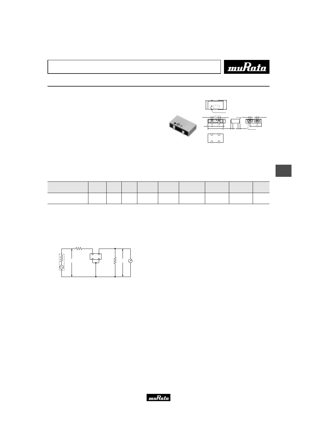
kHz SMD Type CFXC_ Series
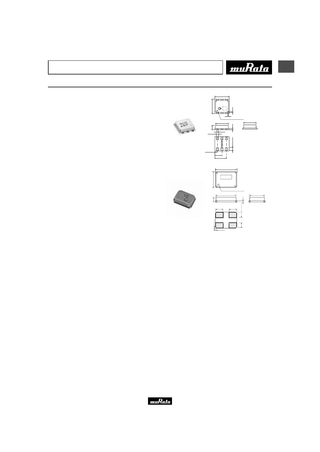
CFXC_ series are very small and high-efficiency
surface mount, ladder type 450/455 kHz ceramic filters
"CERAFIL" for IF section.
Compared to our previous compact surface mounted
6-element product, this ceramic filter has been
significantly downsized to approximately one-third
the original volume and reduced to less than 2 mm in
height.
As for electrical performance, this product, which
consists of 4 elements, provides stop band attenuation
equivalent to that of our previous 6-element product.
The input/output impedance characteristics are also
equivalent to those of the previous product, and
spurious responses in the vicinity of the passing band
can now be eliminated. This allows mobile
telecommunications equipment manufacturers to easily
design the periphery of the IF section and thus
greatly enhance the interference suppression
capability of the equipment.In addition, this ceramic
filter provides flatter group delay time
characteristics than the previous product, and will
effectively work as a component for data transmission
in digital mobile telecommunications systems.
■ Features
1. Compact, thin, and lightweight.
(Size : CFXCA450KBFA-R1: 6.5x6.5x1.9mm
CFXCD450KCFA-R1: 5.2x3.8x1.4mm
Weight: CFXCA series: 225mg
CFXCD series: 75mg)
2. Out-of-band attenuation is increased and spurious
responses are greatly decreased.
3. Group delay time characteristics are flattened.
4. Surface mountable, and reflow soldering can be used
for mounting.
■ Applications
1. IF filters for PDCs.
2. IF filters for various types of pagers.
3. IF filters for various types of analog and digital
cellular telephones.
4. IF filters for radio communication circuits
applicable for PDA or PCMCIA.
5. IF filters for other general mobile wireless
equipment
1.9
6-1.5
±
0.3
5.25
±
0.3
6.5
±
0.3
6.5
±
0.3
(5.8)
(5.5)
3.25
±
0.3
1.25
±
0.3
6-0.6
1.0
Input terminal marking
6-1.0
0.5
1.0
(6) (5) (4)
(1) (2) (3)
(1)
(2) (3)
(6)
(5) (4)
(in mm)
(1) : Input
(3) : Output
(2)(4)(5)(6) : Ground
( ) : Reference
5 0 B
EIAJ
CODE
CFXCA Series
*
5.2
3.8
(3.5)
Input terminal marking
(4.925)
1.4
0.4
4-1.5
4-1.6
±
0.2
4-1.0
4-0.35
4-0.35
(1)
(2)
(4)
(3)
4-1.1
±
0.2
(1)
(2)
(3)(4)
( )
: Input
: Output
: Ground
: Reference
(in mm)
CFXCD Series
Please read rating and
!
CAUTION (for storage and operating, rating, soldering and mounting, handling) in this PDF catalog to prevent smoking and/or burning, etc.
This catalog has only typical specifications. Therefore, you are requested to approve our product specification or to transact the approval sheet for product specificaion before ordering.
!
Note
P05E11.pdf 02.9.2
6
1
!
Note
• Please read rating and
!
CAUTION (for storage and operating, rating, soldering and mounting, handling) in this catalog to prevent smoking and/or burning, etc.
• This catalog has only typical specifications because there is no space for detailed specifications. Therefore, please approve our product specification or transact the approval sheet for product specification before ordering.
Part Number
Nominal Center
Frequency (fn)
(kHz)
3dB
Bandwidth
(kHz)
6dB
Bandwidth
(kHz)
Stop
Bandwidth
(kHz)
Stop Band
Attenuation
(dB)
Stop Band Att.(2)
(dB)
Stop Band Att.(3)
(dB)
Insertion
Loss
(dB)
Ripple
(dB)
GDT Deviation
(
µ
s)
CFXCA450KBFA-R1
450
-
fn
±
15.0
min.
fn
±
50.0 max.
[within 50dB]
47 min.
[within fn
±
100kHz]
-
-
6.0 max.
[at fn]
0.5 max.
[within fn
±
10kHz]
15.0 max.
[within fn
±
10kHz]
CFXCD450KCFA-R1
450
fn
±
9.0 to
±
12.0kHz max.
-
fn
±
35.0 max.
[within 50dB]
30 min.
[at fn
±
25kHz]
55 min.
[within fn
±
40kHz to
±
50kHz]
47 min.
[within fn
±
100kHz]
6.0 max.
[at fn]
0.5 max.
[within fn
±
10.5kHz]
27.0 max.
[within fn
±
10.5kHz]
Spurious:40dB [within 0.1 to 1.0MHz]
Input/Output Impedance:2000 ohm
For safety purposes, connect the output of filters to the IF amplifier through a D.C. blocking capacitor.Avoid applying a direct current to the output of ceramic filters.
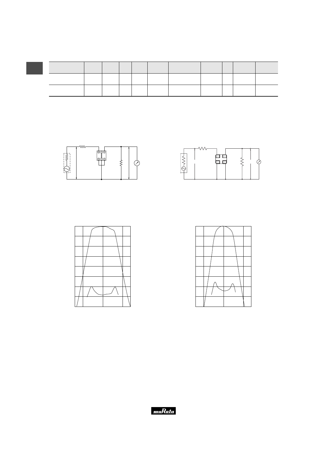
■ Test Circuit
CFXCA Series
S.S.G
0dBm
RF
Voltmeter
Connection
E1
E2
Rg
R2
(1) (2) (3)
(6)
(5) (4)
R1
(1) : Input
(3) : Output
(2)(4)(5)(6) : Ground
R1
+
Rg
=
R2
=
Input/Output Impedance
E1 : S.S.G Output voltage
CFXCD Series
(1)
(2)
(4)
(3)
Rg
S.S.G.
0dBm
R1
R2
(1) Input
(2) Output
(3)(4) Ground
RF Voltmeter
E1
E2
R1 + Rg = R2 = Input/Output Impedance
E1 : S.S.G. Output Voltage
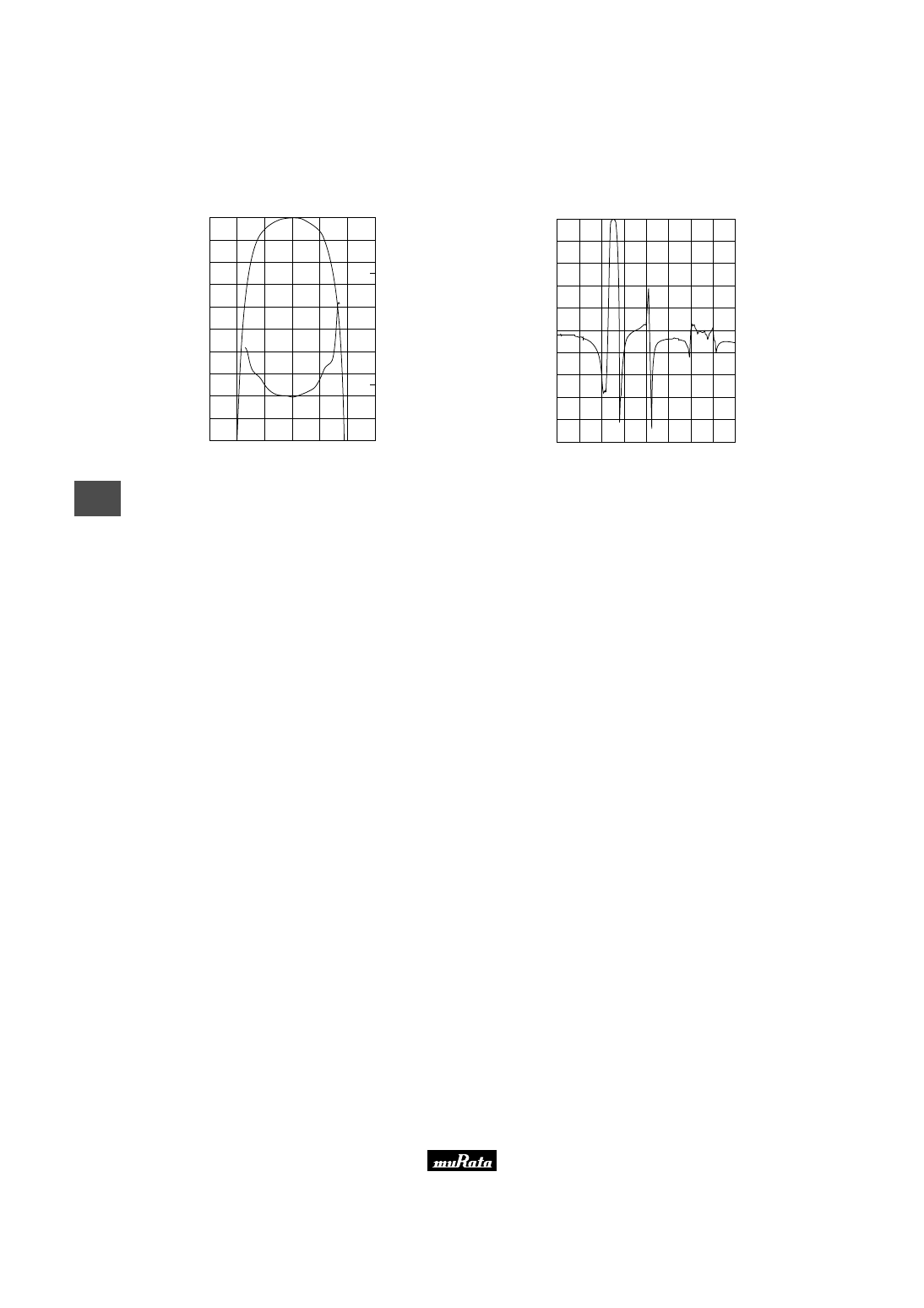
■ Frequency Characteristics
CFXCA450KBFA-R1
A
tt
e
n
u
a
ti
o
n
(
d
B
)
G
.D
.T
.
(
µ
s
e
c
)
Frequency (kHz)
35
40
30
25
20
15
10
5
0
0
50
100
150
200
450.0
475.0
425.0
CFXCD450KCFA-R1
A
tt
e
n
u
a
ti
o
n
(
d
B
)
G
.D
.T
.
(
µ
s
e
c
)
Frequency (kHz)
35
40
30
25
20
15
10
5
0
0
50
100
150
200
450.0
475.0
425.0
Please read rating and
!
CAUTION (for storage and operating, rating, soldering and mounting, handling) in this PDF catalog to prevent smoking and/or burning, etc.
This catalog has only typical specifications. Therefore, you are requested to approve our product specification or to transact the approval sheet for product specificaion before ordering.
!
Note
P05E11.pdf 02.9.2
7
2
!
Note
• Please read rating and
!
CAUTION (for storage and operating, rating, soldering and mounting, handling) in this catalog to prevent smoking and/or burning, etc.
• This catalog has only typical specifications because there is no space for detailed specifications. Therefore, please approve our product specification or transact the approval sheet for product specification before ordering.
Ceramic Filters (CERAFILr)/Ceramic Discriminators for Communications Equipment
CERAFIL
r
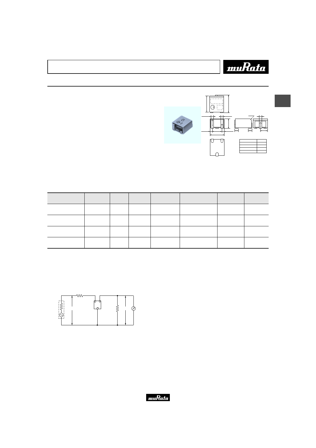
kHz SMD Type SFPCA Series
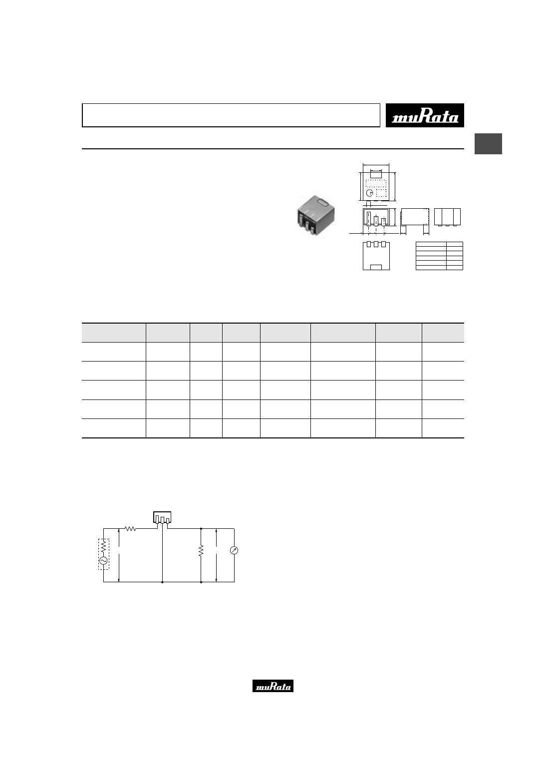
The SFPCA series comprises small, high performance,
economical, thin (5.0mm) filters consisting of 4
ceramic elements.
Their innovative construction is perfect for shrinking
mobile communication products such as cordless phones,
pager and transceivers.
■ Features
1. The filters are mountable by automatic placers.
2. The filters can be reflow soldered and withstand
washing.
3. They are slim, at only 5.0mm maximum thickness.
4. The bandwidth ranges from D to H.
5. Operating temperature range : -20 to +80 (degree C)
Storage temperature range : -40 to +85 (degree C)
7
.5
±
0
.3
5
.0
m
a
x
.
3.0
±
0.3
8
.4
m
a
x
.
2.0
±
0.3
1.5
±
0.3
7.0
±
0.3
0.9
±
0.1
2.0
±
0.3
(1) (2) (3)
1.5
±
0.3
1.6
±
0.3
Connection
(1) : Input
(2) : Ground
(3) : Output
(in mm)
Type
Marking
SFPCA455KD4A-R1
SFPCA455KE4A-R1
SFPCA455KF4A-R1
SFPCA455KG1A-R1
SFPCA455KH1A-R1
D
E
F
G
H
MARKING
EIAJ
CODE
Part Number
Center
Frequency (fo)
(kHz)
6dB
Bandwidth
(kHz)
Stop
Bandwidth
(kHz)
Stop Band
Attenuation
(dB)
Insertion
Loss
(dB)
Ripple
(dB)
Input/Output
Impedance
(ohm)
SFPCA455KD4A-R1
455.0
±
1.5kHz
fn
±
10.0
min.
fn
±
20.0 max.
[within 40dB]
27 min.
[within fn
±
100kHz]
4.0 max.
[at minimum loss point]
2.0 max.
[within fn
±
7kHz]
1500
SFPCA455KE4A-R1
455.0
±
1.5kHz
fn
±
7.5
min.
fn
±
15.0 max.
[within 40dB]
27 min.
[within fn
±
100kHz]
6.0 max.
[at minimum loss point]
1.5 max.
[within fn
±
5kHz]
1500
SFPCA455KF4A-R1
455.0
±
1.5kHz
fn
±
6.0
min.
fn
±
12.5 max.
[within 40dB]
27 min.
[within fn
±
100kHz]
6.0 max.
[at minimum loss point]
1.5 max.
[within fn
±
4kHz]
1500
SFPCA455KG1A-R1
455.0
±
1.0kHz
fn
±
4.5
min.
fn
±
10.0 max.
[within 40dB]
25 min.
[within fn
±
100kHz]
6.0 max.
[at minimum loss point]
1.5 max.
[within fn
±
3kHz]
1500
SFPCA455KH1A-R1
455.0
±
1.0kHz
fn
±
3.0
min.
fn
±
9.0 max.
[within 40dB]
35 min.
[within fn
±
100kHz]
6.0 max.
[at minimum loss point]
1.5 max.
[within fn
±
2kHz]
2000
For safety purposes, connect the output of filters to the IF amplifier through a D.C. blocking capacitor. Avoid applying a direct current to the output of ceramic filters.
(fn) means nominal center frequency 455kHz.
■ Test Circuit
Rg+R1=R2=Input/Output Impedance
E1
R1
Rg
S.S.G.
0dBm
(1)
(2)
(3)
R2
E2
RF Voltmeter
Connection
(1):Input
(2):Ground
(3):Output
Please read rating and
!
CAUTION (for storage and operating, rating, soldering and mounting, handling) in this PDF catalog to prevent smoking and/or burning, etc.
This catalog has only typical specifications. Therefore, you are requested to approve our product specification or to transact the approval sheet for product specificaion before ordering.
!
Note
P05E11.pdf 02.9.2
8
2
!
Note
• Please read rating and
!
CAUTION (for storage and operating, rating, soldering and mounting, handling) in this catalog to prevent smoking and/or burning, etc.
• This catalog has only typical specifications because there is no space for detailed specifications. Therefore, please approve our product specification or transact the approval sheet for product specification before ordering.
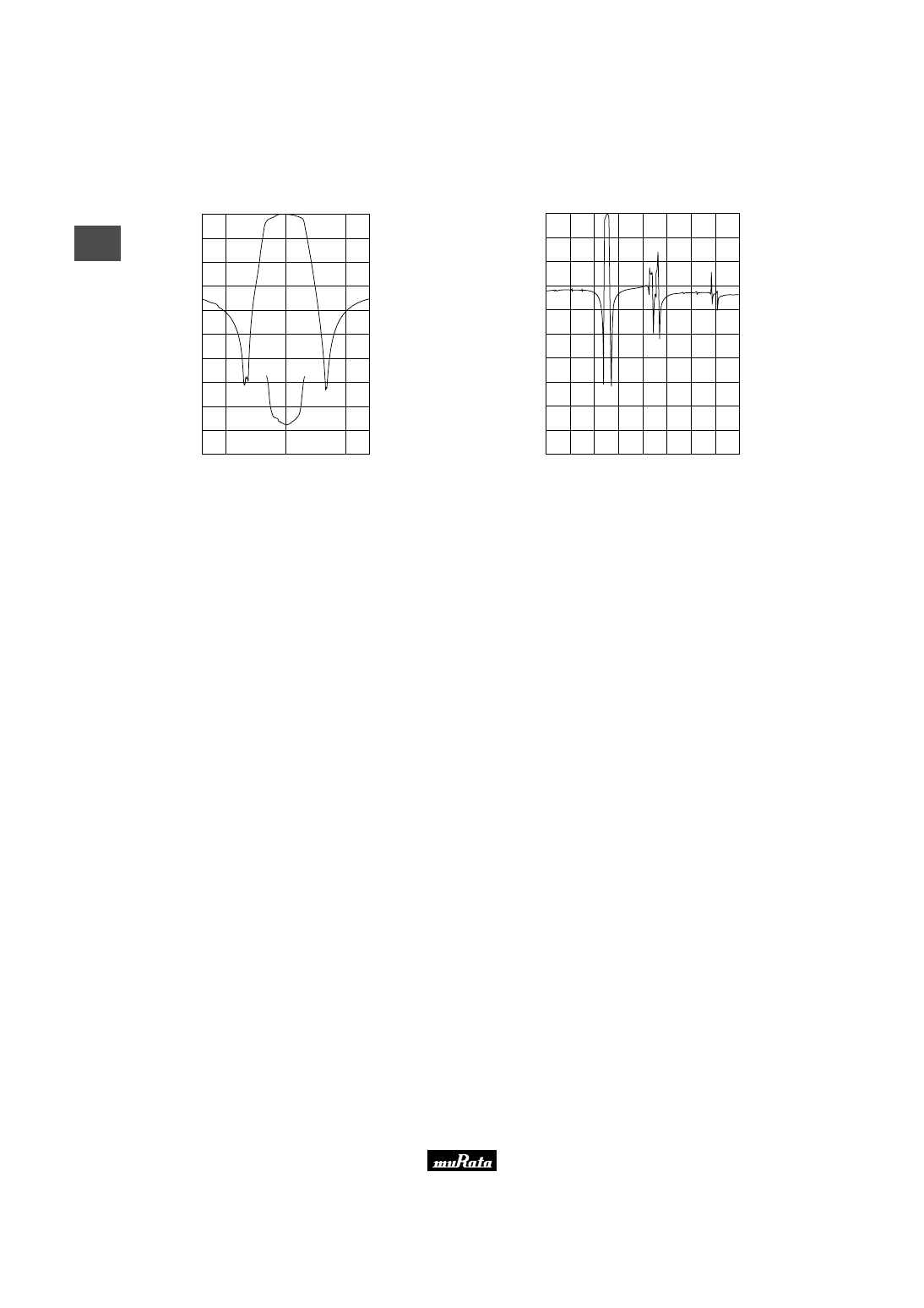
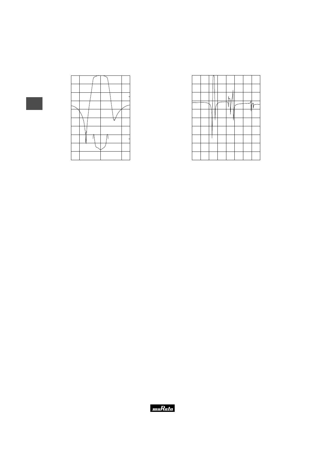
■ Frequency Characteristics
SFPCA455KE4A-R1
100
40
30
20
10
0
A
tt
e
n
u
a
ti
o
n
(
d
B
)
G
.D
.T
.
(
µ
s
e
c
.)
430
455
480
Frequency (kHz)
90
80
70
60
50
0
240
280
320
360
400
40
80
120
160
200
SFPCA455KE4A-R1
100
40
30
20
10
0
A
tt
e
n
u
a
ti
o
n
(
d
B
)
200
Frequency (kHz)
90
80
70
60
50
300
400
500
600
700
800
900
1000
Please read rating and
!
CAUTION (for storage and operating, rating, soldering and mounting, handling) in this PDF catalog to prevent smoking and/or burning, etc.
This catalog has only typical specifications. Therefore, you are requested to approve our product specification or to transact the approval sheet for product specificaion before ordering.
!
Note
P05E11.pdf 02.9.2
9
3
!
Note
• Please read rating and
!
CAUTION (for storage and operating, rating, soldering and mounting, handling) in this catalog to prevent smoking and/or burning, etc.
• This catalog has only typical specifications because there is no space for detailed specifications. Therefore, please approve our product specification or transact the approval sheet for product specification before ordering.
Ceramic Filters (CERAFILr)/Ceramic Discriminators for Communications Equipment
CERAFIL
r
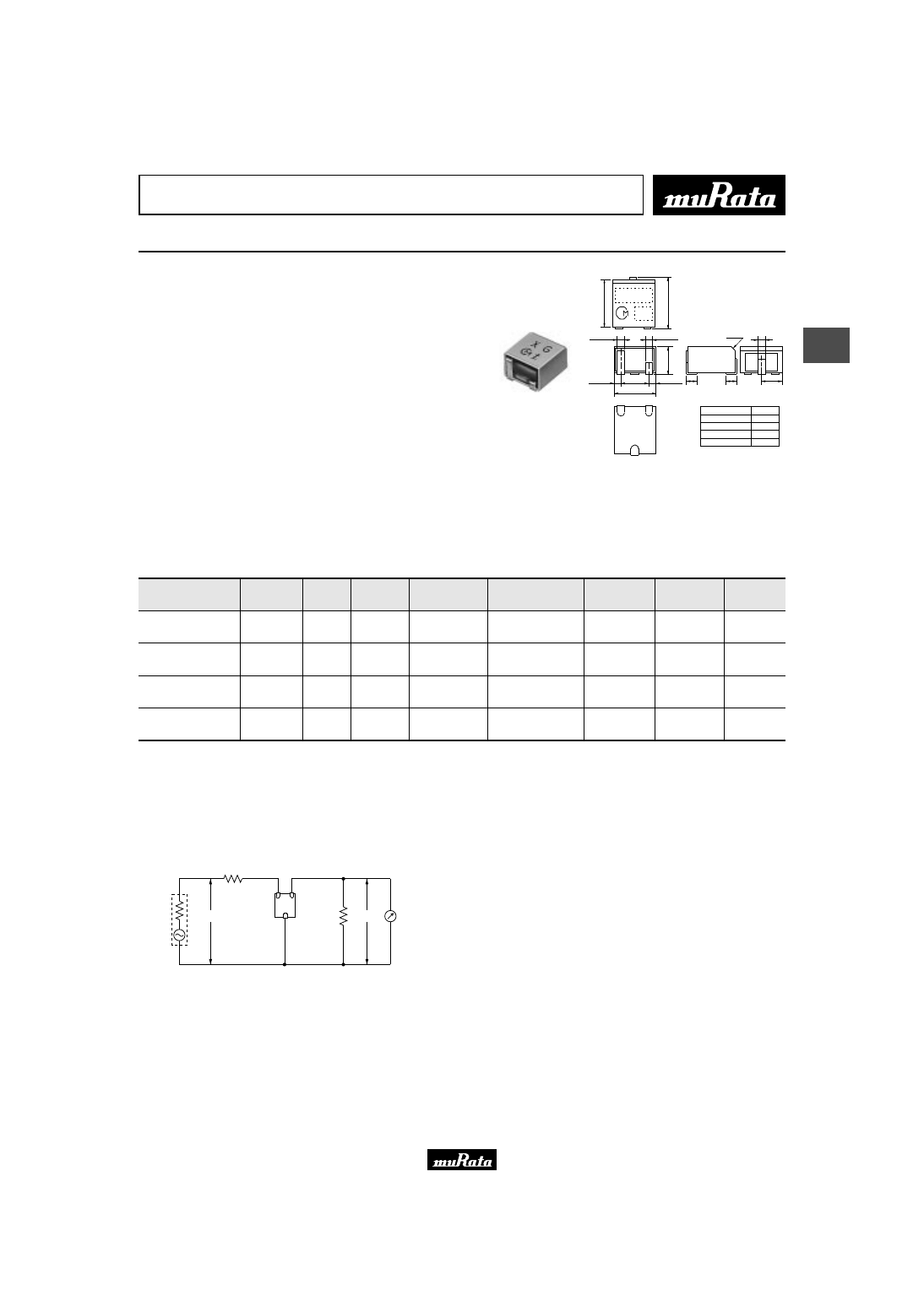
kHz SMD Type CFUCG Series
The CFUCG series comprises small, high performance,
thin (4.0mm) filters consisting of 4 ceramic elements.
Their innovative construction is perfect for shrinking
mobile communication products such as pocket pagers
and cellular phones.
■ Features
1. The filters are mountable by automatic placers.
2. The filters can be reflow soldered and withstand
washing.
3. They are slim, at only 4.0mm maximum thickness,
and have a small mounting area (7.5x6.0mm)
enabling flexible PCB design.
4. The bandwidth ranges from D to G.
5. Operating temperature range : -20 to +80 (degree C)
Storage temperature range : -40 to +85 (degree C)
1.5
±
0.3
3.0
±
0.3
1.0
±
0.1
4.0
±
0.3
6
.5
±
0
.3
7
.5
m
a
x
.
C0.5
1.2
±
0.1
4
.0
m
a
x
.
1.0
±
0.1
(in mm)
Connection
(1) : Input
(2) : Output
(3) : Ground
1.0
±
0.3
1.0
±
0.3
1.5
±
0.3
6.0
±
0.3
(1)
(2)
(3)
Type
CFUCG455KD4A-R0
CFUCG455KE4A-R0
CFUCG455KF4A-R0
CFUCG455KG1A-R0
Marking
D
E
F
G
MARKING
EIAJ
CODE
Part Number
Center
Frequency (fo)
(kHz)
6dB
Bandwidth
(kHz)
Stop
Bandwidth
(kHz)
Stop Band
Attenuation
(dB)
Insertion
Loss
(dB)
Ripple
(dB)
Input/Output
Impedance
(ohm)
CFUCG455KD4A-R0
455.0
±
1.5kHz
fn
±
10.0
min.
fn
±
20.0 max.
[within 40dB]
27 min.
[within fn
±
100kHz]
4.0 max.
[at minimum loss point]
2.0 max.
[within fn
±
7kHz]
1500
CFUCG455KE4A-R0
455.0
±
1.5kHz
fn
±
7.5
min.
fn
±
15.0 max.
[within 40dB]
27 min.
[within fn
±
100kHz]
6.0 max.
[at minimum loss point]
1.5 max.
[within fn
±
5kHz]
1500
CFUCG455KF4A-R0
455.0
±
1.5kHz
fn
±
6.0
min.
fn
±
12.5 max.
[within 40dB]
27 min.
[within fn
±
100kHz]
6.0 max.
[at minimum loss point]
1.5 max.
[within fn
±
4kHz]
1500
CFUCG455KG1A-R0
455.0
±
1.0kHz
fn
±
4.5
min.
fn
±
10.0 max.
[within 40dB]
25 min.
[within fn
±
100kHz]
6.0 max.
[at minimum loss point]
1.5 max.
[within fn
±
3kHz]
1500
For safety purposes, connect the output of filters to the IF amplifier through a D.C. blocking capacitor. Avoid applying a direct current to the output of ceramic filters.
(fn) means nominal center frequency 455kHz.
■ Test Circuit
E1
Rg
S.S.G.
0dBm
R1
RF Voltmeter
Connection
(1) : Input
(2) : Output
(3) : Ground
(2)
(3)
(1)
R2
E2
Rg+R1=R2=Input/Output Impedance
Please read rating and
!
CAUTION (for storage and operating, rating, soldering and mounting, handling) in this PDF catalog to prevent smoking and/or burning, etc.
This catalog has only typical specifications. Therefore, you are requested to approve our product specification or to transact the approval sheet for product specificaion before ordering.
!
Note
P05E11.pdf 02.9.2
10
3
!
Note
• Please read rating and
!
CAUTION (for storage and operating, rating, soldering and mounting, handling) in this catalog to prevent smoking and/or burning, etc.
• This catalog has only typical specifications because there is no space for detailed specifications. Therefore, please approve our product specification or transact the approval sheet for product specification before ordering.
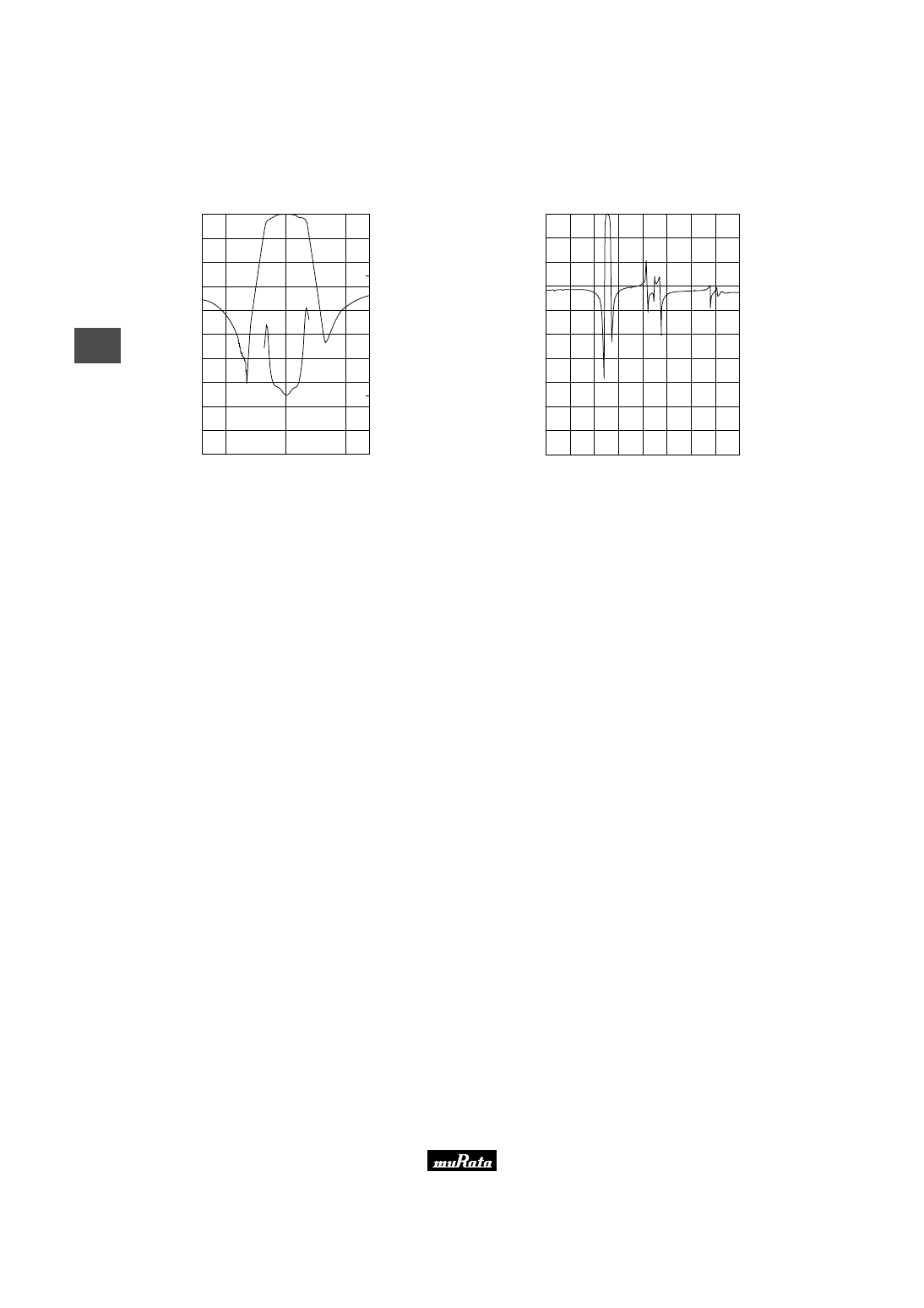
■ Frequency Characteristics
CFUCG455KE4A-R0
100
40
30
20
10
0
A
tt
e
n
u
a
ti
o
n
(
d
B
)
0
100
200
300
400
G
.D
.T
.
(
µ
s
e
c
.)
430
455
480
Frequency (kHz)
90
80
70
60
50
CFUCG455KE4A-R0
100
40
30
20
10
0
A
tt
e
n
u
a
ti
o
n
(
d
B
)
200
Frequency (kHz)
90
80
70
60
50
300
400
500
600
700
800
900
1000
Please read rating and
!
CAUTION (for storage and operating, rating, soldering and mounting, handling) in this PDF catalog to prevent smoking and/or burning, etc.
This catalog has only typical specifications. Therefore, you are requested to approve our product specification or to transact the approval sheet for product specificaion before ordering.
!
Note
P05E11.pdf 02.9.2
11
4
!
Note
• Please read rating and
!
CAUTION (for storage and operating, rating, soldering and mounting, handling) in this catalog to prevent smoking and/or burning, etc.
• This catalog has only typical specifications because there is no space for detailed specifications. Therefore, please approve our product specification or transact the approval sheet for product specification before ordering.
Ceramic Filters (CERAFILr)/Ceramic Discriminators for Communications Equipment
CERAFIL
r
kHz SMD Type CFUCG_X Series
The CFUCG_X series comprises small, high performance,
thin (4.0mm) filters consisting of 4 ceramic elements.
The filters exhibit an extremely flat GDT
characteristic combined with a narrow bandwidth.
The filters are recommended for narrow band digital
communication applications.
■ Features
1. The filters are mountable by automatic placers.
2. The filters can be reflow soldered and withstand
washing.
3. They are slim, at only 4.0mm maximum thickness,
and have a small mounting area (7.5x6.0mm)
enabling flexible PCB design.
4. The bandwidth ranges from E to H.
5. Operating temperature range : -20 to +80 (degree C)
Storage temperature range : -40 to +85 (degree C)
1.5
±
0.3
3.0
±
0.3
1.0
±
0.1
4.0
±
0.3
6
.5
±
0
.3
7
.5
m
a
x
.
C0.5
1.2
±
0.1
4
.0
m
a
x
.
1.0
±
0.1
(in mm)
Connection
(1) : Input
(2) : Output
(3) : Ground
1.0
±
0.3
1.0
±
0.3
1.5
±
0.3
6.0
±
0.3
(1)
(2)
(3)
Type
CFUCG455KE4X-R0
CFUCG455KF4X-R0
CFUCG455KG1X-R0
CFUCG455KH1X-R0
Marking
XE
XF
XG
XH
MARKING
EIAJ
CODE
Part Number
Center
Frequency (fo)
(kHz)
6dB
Bandwidth
(kHz)
Stop
Bandwidth
(kHz)
Stop Band
Attenuation
(dB)
Insertion
Loss
(dB)
Ripple
(dB)
GDT Deviation
(
µ
s)
Input/Output
Impedance
(ohm)
CFUCG455KE4X-R0
455.0
±
1.5kHz
fn
±
7.5
min.
fn
±
17.5 max.
[within 40dB]
27 min.
[within fn
±
100kHz]
6.0 max.
[at minimum loss point]
1.0 max.
[within fn
±
5kHz]
25.0 max.
[within fn
±
5kHz]
1500
CFUCG455KF4X-R0
455.0
±
1.5kHz
fn
±
6.0
min.
fn
±
15.0 max.
[within 40dB]
27 min.
[within fn
±
100kHz]
6.0 max.
[at minimum loss point]
1.0 max.
[within fn
±
4kHz]
25.0 max.
[within fn
±
4kHz]
1500
CFUCG455KG1X-R0
455.0
±
1.0kHz
fn
±
4.5
min.
fn
±
12.5 max.
[within 40dB]
25 min.
[within fn
±
100kHz]
6.0 max.
[at minimum loss point]
1.0 max.
[within fn
±
3kHz]
25.0 max.
[within fn
±
3kHz]
1500
CFUCG455KH1X-R0
455.0
±
1.0kHz
fn
±
3.0
min.
fn
±
10.0 max.
[within 40dB]
25 min.
[within fn
±
100kHz]
7.0 max.
[at minimum loss point]
1.0 max.
[within fn
±
2kHz]
25.0 max.
[within fn
±
2kHz]
1500
For safety purposes, connect the output of filters to the IF amplifier through a D.C. blocking capacitor. Avoid applying a direct current to the output of ceramic filters.
(fn) means nominal center frequency 455kHz.
■ Test Circuit
E1
Rg
S.S.G.
0dBm
R1
RF Voltmeter
Connection
(1) : Input
(2) : Output
(3) : Ground
(2)
(3)
(1)
R2
E2
Rg+R1=R2=Input/Output Impedance
Please read rating and
!
CAUTION (for storage and operating, rating, soldering and mounting, handling) in this PDF catalog to prevent smoking and/or burning, etc.
This catalog has only typical specifications. Therefore, you are requested to approve our product specification or to transact the approval sheet for product specificaion before ordering.
!
Note
P05E11.pdf 02.9.2
12
4
!
Note
• Please read rating and
!
CAUTION (for storage and operating, rating, soldering and mounting, handling) in this catalog to prevent smoking and/or burning, etc.
• This catalog has only typical specifications because there is no space for detailed specifications. Therefore, please approve our product specification or transact the approval sheet for product specification before ordering.
■ Frequency Characteristics
CFUCG455KE4X-R0
100
40
30
20
10
0
A
tt
e
n
u
a
ti
o
n
(
d
B
)
0
50
100
150
200
G
.D
.T
.
(
µ
s
e
c
.)
430
455
480
Frequency (kHz)
90
80
70
60
50
CFUCG455KE4X-R0
100
40
30
20
10
0
A
tt
e
n
u
a
ti
o
n
(
d
B
)
200
Frequency (kHz)
90
80
70
60
50
300
400
500
600
700
800
900
1000
Please read rating and
!
CAUTION (for storage and operating, rating, soldering and mounting, handling) in this PDF catalog to prevent smoking and/or burning, etc.
This catalog has only typical specifications. Therefore, you are requested to approve our product specification or to transact the approval sheet for product specificaion before ordering.
!
Note
P05E11.pdf 02.9.2
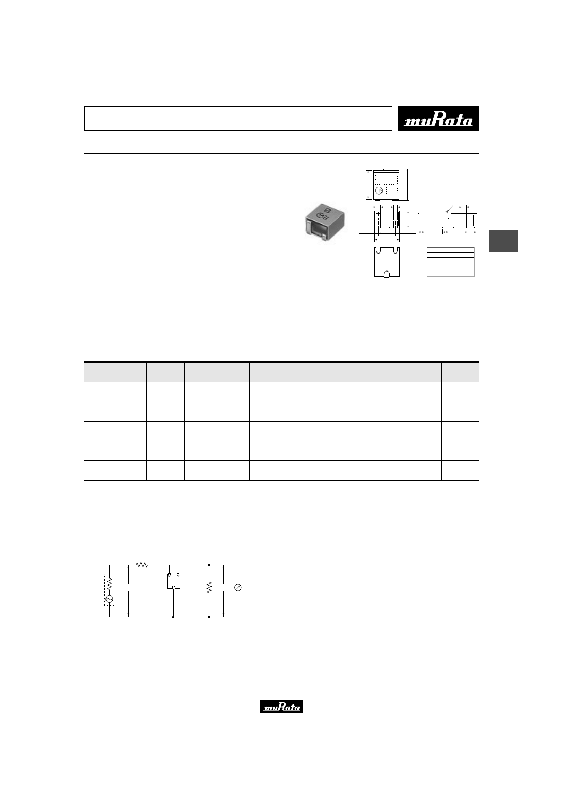
13
5
!
Note
• Please read rating and
!
CAUTION (for storage and operating, rating, soldering and mounting, handling) in this catalog to prevent smoking and/or burning, etc.
• This catalog has only typical specifications because there is no space for detailed specifications. Therefore, please approve our product specification or transact the approval sheet for product specification before ordering.
Ceramic Filters (CERAFILr)/Ceramic Discriminators for Communications Equipment
CERAFIL
r
kHz SMD Type CFUCF Series
The CFUCF series comprises small, high performance,
thin (4.0mm) filters consisting of 4 ceramic elements.
The filters exhibit an extremely flat GDT
characteristic.
The filters are recommended for digital
communication applications and are perfect in hand
held cellular phones, etc.
■ Features
1. The filters are mountable by automatic placers.
2. The filters can be reflow soldered and withstand
washing.
3. They are slim, at only 4.0mm maximum thickness,
and have a small mounting area (7.5x6.0mm)
enabling flexible PCB design.
4. The bandwidth ranges from A to E.
5. Operating temperature range : -20 to +80 (degree C)
Storage temperature range : -40 to +85 (degree C)
1.5
±
0.3
3.0
±
0.3
1.0
±
0.1
4.0
±
0.3
6
.5
±
0
.3
7
.5
m
a
x
.
C0.5
1.2
±
0.1
4
.0
m
a
x
.
1.0
±
0.1
(in mm)
Connection
(1) : Input
(2) : Output
(3) : Ground
1.0
±
0.3
1.0
±
0.3
1.5
±
0.3
6.0
±
0.3
(1)
(2)
(3)
Type
CFUCF455KA2X-R0
CFUCF455KB4X-R0
CFUCF455KC4X-R0
CFUCF455KD1X-R0
CFUCF455KE1X-R0
Marking
A
B
C
D
E
MARKING
EIAJ
CODE
Part Number
Center
Frequency (fo)
(kHz)
6dB
Bandwidth
(kHz)
Stop
Bandwidth
(kHz)
Stop Band
Attenuation
(dB)
Insertion
Loss
(dB)
Ripple
(dB)
GDT Deviation
(
µ
s)
Input/Output
Impedance
(ohm)
CFUCF455KA2X-R0
455.0
±
2.0kHz
fn
±
17.5
min.
fn
±
40.0 max.
[within 40dB]
25 min.
[within fn
±
100kHz]
4.0 max.
[at minimum loss point]
1.0 max.
[within fn
±
12kHz]
15.0 max.
[within fn
±
12kHz]
1000
CFUCF455KB4X-R0
455.0
±
1.5kHz
fn
±
15.0
min.
fn
±
35.0 max.
[within 40dB]
25 min.
[within fn
±
100kHz]
5.0 max.
[at minimum loss point]
1.0 max.
[within fn
±
10kHz]
15.0 max.
[within fn
±
10kHz]
1000
CFUCF455KC4X-R0
455.0
±
1.5kHz
fn
±
12.5
min.
fn
±
30.0 max.
[within 40dB]
25 min.
[within fn
±
100kHz]
6.0 max.
[at minimum loss point]
1.0 max.
[within fn
±
8kHz]
15.0 max.
[within fn
±
8kHz]
1000
CFUCF455KD1X-R0
455.0
±
1.0kHz
fn
±
10.0
min.
fn
±
25.0 max.
[within 40dB]
23 min.
[within fn
±
100kHz]
7.0 max.
[at minimum loss point]
1.0 max.
[within fn
±
7kHz]
20.0 max.
[within fn
±
7kHz]
1500
CFUCF455KE1X-R0
455.0
±
1.0kHz
fn
±
7.5
min.
fn
±
20.0 max.
[within 40dB]
23 min.
[within fn
±
100kHz]
8.0 max.
[at minimum loss point]
1.0 max.
[within fn
±
5kHz]
20.0 max.
[within fn
±
5kHz]
1500
For safety purposes, connect the output of filters to the IF amplifier through a D.C. blocking capacitor. Avoid applying a direct current to the output of ceramic filters.
(fn) means nominal center frequency 455kHz.
■ Test Circuit
E1
Rg
S.S.G.
0dBm
R1
RF Voltmeter
Connection
(1) : Input
(2) : Output
(3) : Ground
(2)
(3)
(1)
R2
E2
Rg+R1=R2=Input/Output Impedance
Please read rating and
!
CAUTION (for storage and operating, rating, soldering and mounting, handling) in this PDF catalog to prevent smoking and/or burning, etc.
This catalog has only typical specifications. Therefore, you are requested to approve our product specification or to transact the approval sheet for product specificaion before ordering.
!
Note
P05E11.pdf 02.9.2
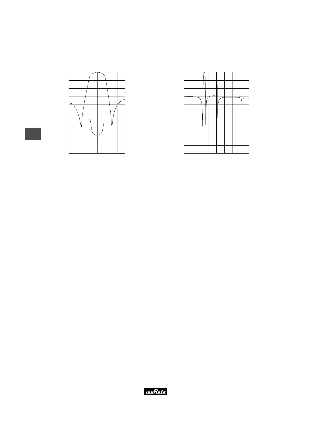
14
5
!
Note
• Please read rating and
!
CAUTION (for storage and operating, rating, soldering and mounting, handling) in this catalog to prevent smoking and/or burning, etc.
• This catalog has only typical specifications because there is no space for detailed specifications. Therefore, please approve our product specification or transact the approval sheet for product specification before ordering.
■ Frequency Characteristics
CFUCF455KE1X-R0
100
40
30
20
10
0
A
tt
e
n
u
a
ti
o
n
(
d
B
)
0
50
100
150
200
G
.D
.T
.
(
µ
s
e
c
.)
430
455
480
Frequency (kHz)
90
80
70
60
50
CFUCF455KE1X-R0
100
40
30
20
10
0
A
tt
e
n
u
a
ti
o
n
(
d
B
)
200
Frequency (kHz)
90
80
70
60
50
300
400
500
600
700
800
900
1000
Please read rating and
!
CAUTION (for storage and operating, rating, soldering and mounting, handling) in this PDF catalog to prevent smoking and/or burning, etc.
This catalog has only typical specifications. Therefore, you are requested to approve our product specification or to transact the approval sheet for product specificaion before ordering.
!
Note
P05E11.pdf 02.9.2
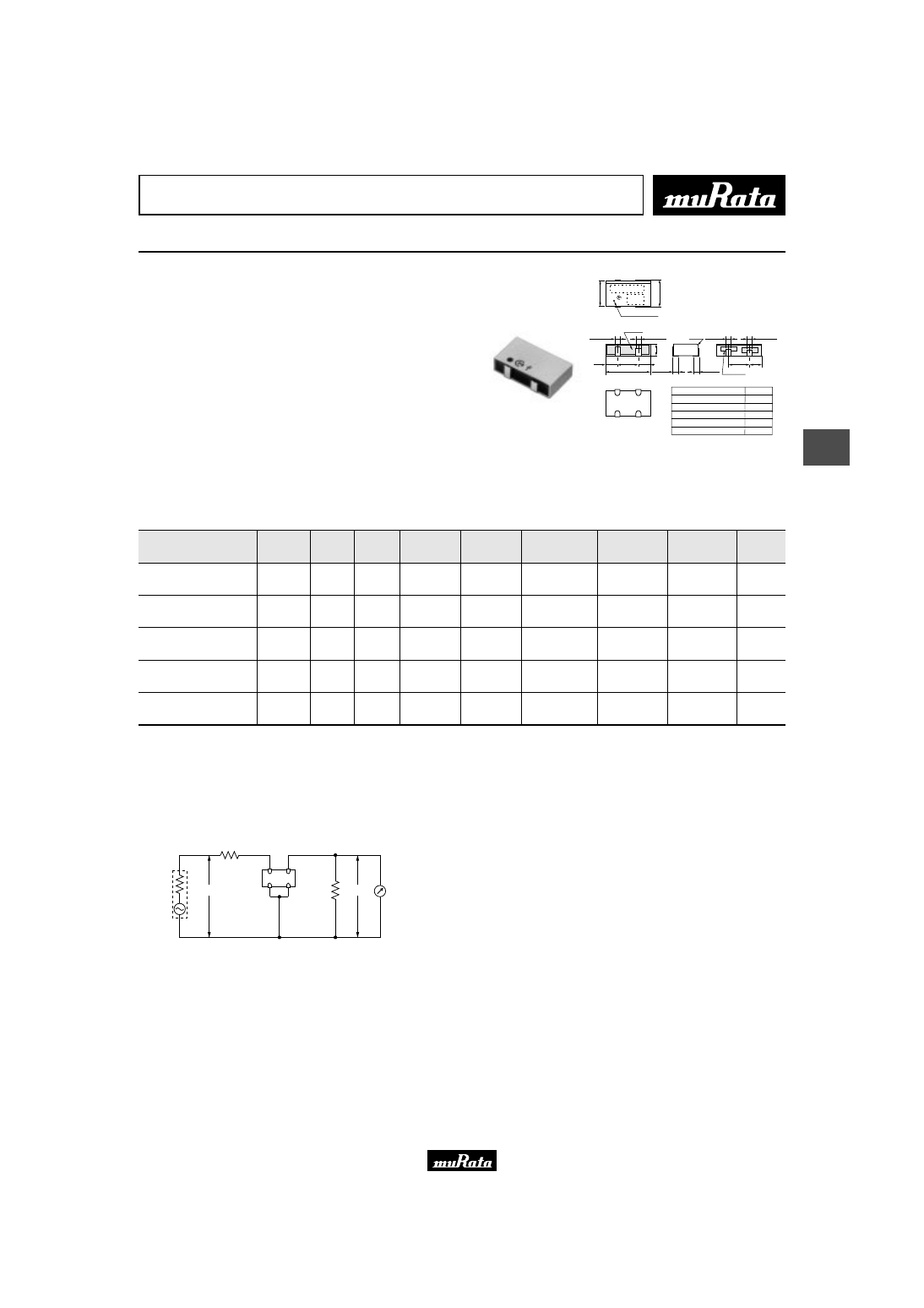
15
6
!
Note
• Please read rating and
!
CAUTION (for storage and operating, rating, soldering and mounting, handling) in this catalog to prevent smoking and/or burning, etc.
• This catalog has only typical specifications because there is no space for detailed specifications. Therefore, please approve our product specification or transact the approval sheet for product specification before ordering.
Ceramic Filters (CERAFILr)/Ceramic Discriminators for Communications Equipment
CERAFIL
r
kHz SMD Type CFWCA Series
The CFWCA series comprises small, high performance,
thin (3.0mm) filters consisting of 6 ceramic elements.
The filters are recommend for pager or hand held
cellular phones.
■ Features
1. The filters are mountable by automatic placers.
2. The filters can be reflow soldered and withstand
washing.
3. They are slim, at only 3.0mm maximum thickness.
4. The filters are wide bandwidth, flat GDT within
pass band.
5. Operating temperature range : -20 to +80 (degree C)
Storage temperature range : -40 to +85 (degree C)
MARKING
6
.5
7
.5
m
a
x
.
3
.0
m
a
x
.
11.5
5.5
3.0
1.2
±
0.1
1.5
±
0.3
1.2
±
0.1
1.2
±
0.1
1.5
±
0.3
1.2
±
0.1
C0.3
3.0
3.0
5.5
Dot marking
Sealing
Sealing
: Input
: Output
: Ground
(1)
(1)
(2)
(2)
(4)
(3)
(3)(4)
EIAJ
CODE
Tolerance
±
0.3mm
in mm
(
)
Type
CFWCA450KDFA-R0
CFWCA450KEFA-R0
CFWCA450KEFA001-R0
CFWCA450KFFA-R0
CFWCA450KGFA-R0
Marking
50D
50E
50E1
50F
50G
Part Number
Nominal Center
Frequency (fn)
(kHz)
3dB
Bandwidth
(kHz)
6dB
Bandwidth
(kHz)
Stop
Bandwidth
(kHz)
Stop Band
Attenuation
(dB)
Stop Band Att.(2)
(dB)
Insertion
Loss
(dB)
Ripple
(dB)
Input/Output
Impedance
(ohm)
CFWCA450KDFA-R0
450
-
fn
±
10.0
min.
fn
±
20.0 max.
[within 50dB]
50 min.
[within fn
±
100kHz]
-
4.0 max.
[at minimum loss point]
3.0 max.
[within fn
±
7kHz]
1500
CFWCA450KEFA-R0
450
-
fn
±
7.5
min.
fn
±
15.0 max.
[within 50dB]
50 min.
[within fn
±
100kHz]
-
6.0 max.
[at minimum loss point]
3.0 max.
[within fn
±
5kHz]
1500
CFWCA450KEFA001-R0
450
fn
±
6.5 min.
-
fn
±
15.0 max.
[within 50dB]
55 min.
[fn
±
18 to
±
33kHz]
50 min.
[within fn
±
100kHz]
4.0 max.
[at fn]
3.0 max.
[within fn
±
6.5kHz]
1500
CFWCA450KFFA-R0
450
-
fn
±
6.0
min.
fn
±
12.5 min.
[within 50dB]
50 min.
[within fn
±
100kHz]
-
6.0 max.
[at minimum loss point]
3.0 max.
[within fn
±
4kHz]
1500
CFWCA450KGFA-R0
450
-
fn
±
4.5
min.
fn
±
11.0 max.
[within 50dB]
50 min.
[within fn
±
100kHz]
-
6.0 max.
[at minimum loss point]
2.0 max.
[within fn
±
3kHz]
1500
For safety purposes, connect the output of filters to the IF amplifier through a D.C. blocking capacitor. Avoid applying a direct current to the output of ceramic filters.
■ Test Circuit
E1
Rg
S.S.G.
0dBm
R1
RF Voltmeter
Connection
(1) : Input
(2) : Output
(3)(4) : Ground
(2)
(4)
(1)
R2
E2
(3)
Rg+R1=R2=Input/Output Impedance
Please read rating and
!
CAUTION (for storage and operating, rating, soldering and mounting, handling) in this PDF catalog to prevent smoking and/or burning, etc.
This catalog has only typical specifications. Therefore, you are requested to approve our product specification or to transact the approval sheet for product specificaion before ordering.
!
Note
P05E11.pdf 02.9.2
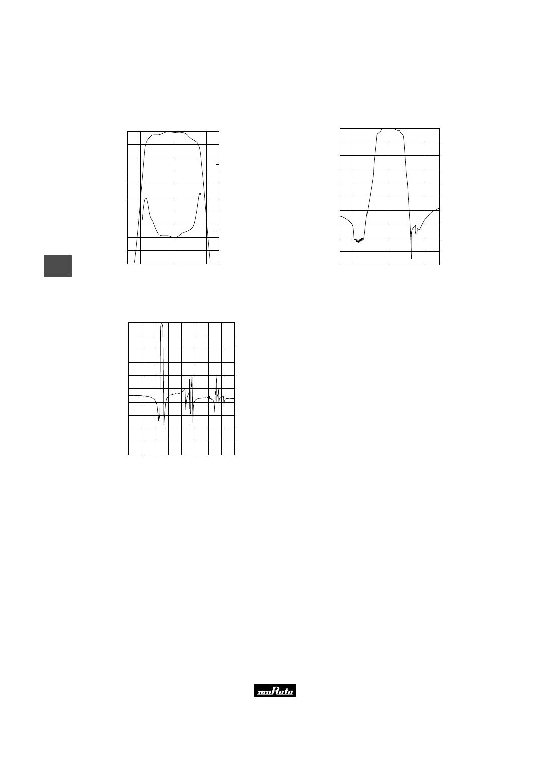
16
6
!
Note
• Please read rating and
!
CAUTION (for storage and operating, rating, soldering and mounting, handling) in this catalog to prevent smoking and/or burning, etc.
• This catalog has only typical specifications because there is no space for detailed specifications. Therefore, please approve our product specification or transact the approval sheet for product specification before ordering.
■ Frequency Characteristics
CFWCA450KEFA001-R0
Frequency (kHz)
A
tt
e
n
u
a
ti
o
n
(
d
B
)
G
.D
.T
.
(
µ
s
e
c
.)
400
300
200
100
0
440.0
450.0
460.0
0
4
8
12
16
20
24
28
32
36
40
CFWCA450KEFA001-R0
10
0
20
30
40
50
60
70
80
90
100
430
455
480
Frequency (kHz)
A
tt
e
n
u
a
ti
o
n
(
d
B
)
CFWCA450KEFA001-R0
Frequency (kHz)
A
tt
e
n
u
a
ti
o
n
(
d
B
)
200
300
400
500
600
700
800
900
1000
0
10
20
30
40
50
60
70
80
90
100
Please read rating and
!
CAUTION (for storage and operating, rating, soldering and mounting, handling) in this PDF catalog to prevent smoking and/or burning, etc.
This catalog has only typical specifications. Therefore, you are requested to approve our product specification or to transact the approval sheet for product specificaion before ordering.
!
Note
P05E11.pdf 02.9.2
17
7
!
Note
• Please read rating and
!
CAUTION (for storage and operating, rating, soldering and mounting, handling) in this catalog to prevent smoking and/or burning, etc.
• This catalog has only typical specifications because there is no space for detailed specifications. Therefore, please approve our product specification or transact the approval sheet for product specification before ordering.
Ceramic Filters (CERAFILr)/Ceramic Discriminators for Communications Equipment
CERAFIL
r
kHz SMD Type CFWCA_Y Series
The CFWCA_Y series comprises small, high performance,
thin (3.0mm) filters consisting of 6 ceramic elements.
The filters are recommend for digital communication
applications and are perfect in hand held cellular
phones.
■ Features
1. The filters are mountable by automatic placers, and
can be reflow soldered, and withstand washing.
2. They are slim, at only 3.0mm maximum thickness.
3. The filters are wide bandwidth, flat GDT within
pass band.
4. Operating temperature range : -20 to +80 (degree C)
Storage temperature range : -40 to +85 (degree C)
Y50
B 1
6
.5
7
.5
m
a
x
.
3
.0
m
a
x
.
11.5
5.5
3.0
1.2
±
0.1
1.5
±
0.3
1.2
±
0.1
1.2
±
0.1
1.5
±
0.3
1.2
±
0.1
C0.3
3.0
3.0
5.5
Dot marking
Sealing
Sealing
Tolerance
±
0.3mm
in mm
: Input
: Output
: Ground
(1)
(1)
(2)
(2)
(4)
(3)
(3)(4)
EIAJ
CODE
(
)
Part Number
Nominal Center
Frequency (fn)
(kHz)
3dB
Bandwidth
(kHz)
6dB
Bandwidth
(kHz)
Stop
Bandwidth
(kHz)
Stop Band
Attenuation
(dB)
Insertion
Loss
(dB)
Spurious
Response
(dB)
GDT Deviation
(
µ
s)
Input/Output
Impedance
(ohm)
CFWCA450KBFY001-R0
450
fn
±
11.5 min.
fn
±
13.0
min.
fn
±
30.0 max.
[within 50dB]
45 min.
[within fn
±
100kHz]
4.0 max.
[at minimum loss point]
20 min.
[within 0.1 to 1.0MHz]
30.0 max.
[within fn
±
10kHz]
1000
For safety purposes, connect the output of filters to the IF amplifier through a D.C. blocking capacitor. Avoid applying a direct current to the output of ceramic filters.
■ Test Circuit
E1
Rg
S.S.G.
0dBm
R1
RF Voltmeter
Connection
(1) : Input
(2) : Output
(3)(4) : Ground
(2)
(4)
(1)
R2
E2
(3)
Rg+R1=R2=Input/Output Impedance
Please read rating and
!
CAUTION (for storage and operating, rating, soldering and mounting, handling) in this PDF catalog to prevent smoking and/or burning, etc.
This catalog has only typical specifications. Therefore, you are requested to approve our product specification or to transact the approval sheet for product specificaion before ordering.
!
Note
P05E11.pdf 02.9.2
18
7
!
Note
• Please read rating and
!
CAUTION (for storage and operating, rating, soldering and mounting, handling) in this catalog to prevent smoking and/or burning, etc.
• This catalog has only typical specifications because there is no space for detailed specifications. Therefore, please approve our product specification or transact the approval sheet for product specification before ordering.
■ Frequency Characteristics
CFWCA450KBFY001-R0
A
tt
e
n
u
a
ti
o
n
(
d
B
)
G
.D
.T
.
(
µ
s
e
c
.)
200
150
100
50
0
420
430
440
450
460
470
480
Frequency (kHz)
0
2
4
6
8
10
12
14
16
18
20
CFWCA450KBFY001-R0
Frequency (kHz)
A
tt
e
n
u
a
ti
o
n
(
d
B
)
200
300
400
500
600
700
800
900
1000
0
10
20
30
40
50
60
70
80
90
100
Please read rating and
!
CAUTION (for storage and operating, rating, soldering and mounting, handling) in this PDF catalog to prevent smoking and/or burning, etc.
This catalog has only typical specifications. Therefore, you are requested to approve our product specification or to transact the approval sheet for product specificaion before ordering.
!
Note
P05E11.pdf 02.9.2
kHz SMD Type CERAFIL
r
Notice
19
7
!
Note
• Please read rating and
!
CAUTION (for storage and operating, rating, soldering and mounting, handling) in this catalog to prevent smoking and/or burning, etc.
• This catalog has only typical specifications because there is no space for detailed specifications. Therefore, please approve our product specification or transact the approval sheet for product specification before ordering.
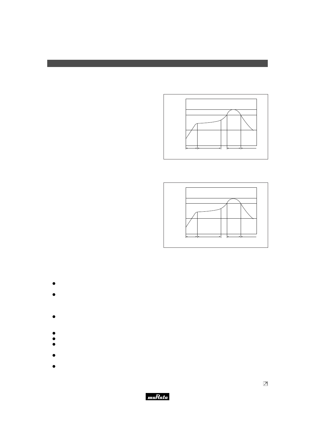
■ CFXC_ Series Notice (Soldering and Mounting)
Filter is soldered twice within the following temperature
condition and then being placed in natural condition for
24 hours.
1. Standard Reflow Soldering Condition
(1) Reflow
The component cannot be withstand washing.
2. Wash
Elecrode is directly contacted with the tip of soldering iron
of +350
±
5
°
C for 3
±
1 seconds, and then being placed in
natural condition for 24 hours.
(2) Soldering Iron
Peak
(240
°
C max.)
Heating
(200
°
C)
Gradual
Cooling
Pre-heating
(140-160
°
C)
100
200
240
T
e
m
p
e
ra
tu
re
(
°
C
)
30sec. min. 60sec.-120sec.
50sec. max. 120sec. min.
■ SFPCA/CFUCG/CFUCF Series Notice (Soldering and Mounting)
Filter is soldered one time within the following
temperature condition and then being placed in natural
condition for 24 hours.
1. Standard Reflow Soldering Condition
(1) Reflow
CFC alternatives(HCFC Series), Isopropyl Alcohol(IPA),
Water(Demineralized Water), Cleaning Water
Solution(Cleanthrough-750H, Pine Alha 100S),
Silicon(Technocare FRW)
2. Wash
(1) Cleaning Solvent
Immersion Wash
2 minutes max. in above solvent at +60
°
C max.
Shower or Rinse Wash
2 minutes max. in above solvent at +60
°
C max.
(2) Cleaning Conditions
When components are immersed in solvent, be sure to
maintain the temperature of components below the
temperature of solvent.
Please do not use ultrasonic cleaning.
Total washing time should be within 4minutes.
Please ensure the component is thoroughly evaluated
in your application circuit.
Please do not use chlorine, petroleum and alkali
cleaning solvent.
If you plan to use any other type of solvents, please
consult with Murata or MUrata representative prior to
using.
(3) Notice
Electrode is directly with the tip of soldering iron of +350
±
5
°
C for 3
±
1 seconds, and then being placed in natural
condition for 24hours.
(2) Soldering Iron
Peak
(235
°
C max.)
Heating
(200
°
C)
Gradual
Cooling
Pre-heating
(140-160
°
C)
100
200
240
T
e
m
p
e
ra
tu
re
(
°
C
)
30sec. min. 60sec.-120sec.
50sec. max. 120sec. min.
Continued on the following page.
Please read rating and
!
CAUTION (for storage and operating, rating, soldering and mounting, handling) in this PDF catalog to prevent smoking and/or burning, etc.
This catalog has only typical specifications. Therefore, you are requested to approve our product specification or to transact the approval sheet for product specificaion before ordering.
!
Note
P05E11.pdf 02.9.2
kHz SMD Type CERAFIL
r
Notice
20
7
!
Note
• Please read rating and
!
CAUTION (for storage and operating, rating, soldering and mounting, handling) in this catalog to prevent smoking and/or burning, etc.
• This catalog has only typical specifications because there is no space for detailed specifications. Therefore, please approve our product specification or transact the approval sheet for product specification before ordering.
Continued from the preceding page.
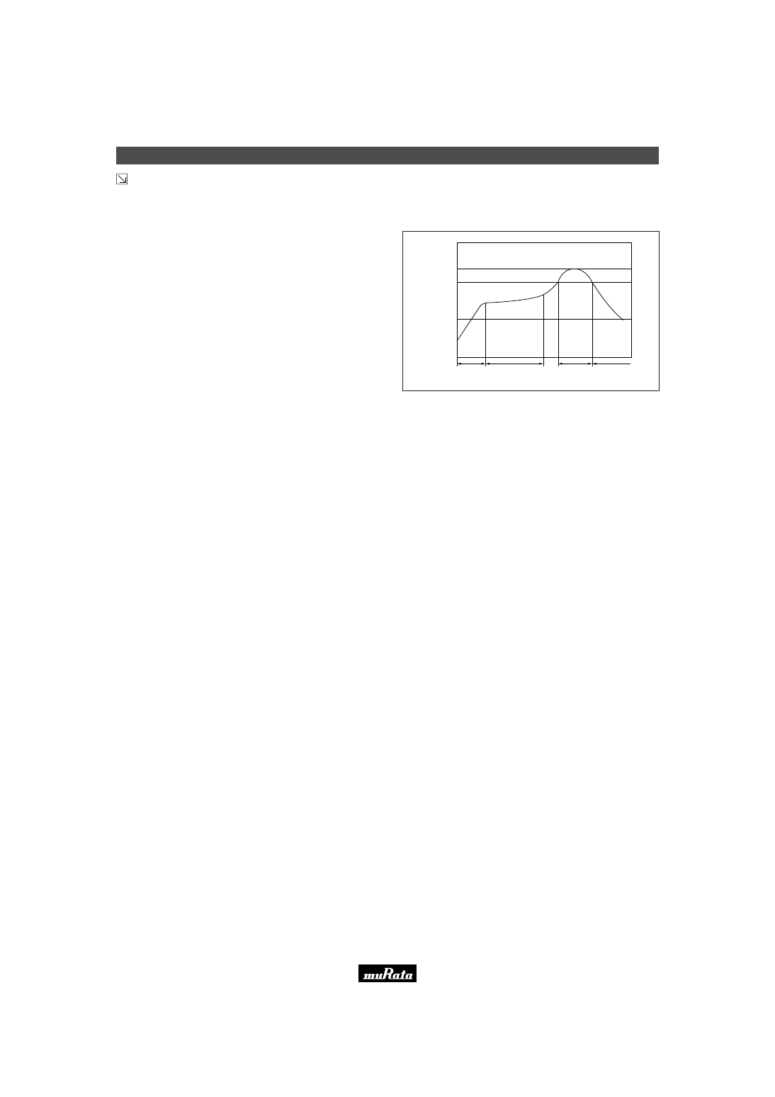
■ CFWCA Series Notice (Soldering and Mounting)
Filter is soldered once within the following temperature
condition and then being placed in natural condition for
24 hours.
1. Standard Reflow Soldering Condition
(1) Reflow
The component cannot be withstand washing.
2. Wash
Electrode is directly contacted with the tip of soldering
iron of +350
±
5
°
C for 3
±
1 seconds, and then being placed
in natural condition for 24hours.
(2) Soldering Iron
Peak
(240
°
C max.)
Heating
(200
°
C)
Gradual
Cooling
Pre-heating
(140-160
°
C)
100
200
240
T
e
m
p
e
ra
tu
re
(
°
C
)
30sec. min. 60sec.-120sec.
50sec. max. 120sec. min.
■ CFXC_/CFWCA Series Notice (Handling)
1. The component will be damaged when an excessive
stress is applied.
2. Use coupling capacitors to prevent applying D.C.
voltage between input-ground, output-ground of
"CERAFIL" as D.C. current may harm the component.
3. Do not clean or wash the component as it's not
hermetically sealed.
4. Do not apply conformal coating onto the component
as it's not hermetically sealed.
5. Do not use strong acidity flux, more than 0.2wt%
chlorine content, in re-flow soldering.
■ SFPCA/CFUCG/CFUCF Series Notice (Handling)
1. The component will be damaged when an excessive
stress is applied.
2. Use coupling capacitors to prevent applying D.C.
voltage between input-ground, output-ground of
"CERAFIL" as D.C. current may harm the component.
3. In the case that the component is cleaned, confirm
no reliability degradation is created.
4. In case of covering filter with over coat,
conditions such as material of resin, cure
temperature, and so on should be evaluated well.
5. Do not use strong acidity flux, more than 0.2wt%
chlorine content, in re-flow soldering.
6. The product, packed in the moisture-proof bag
(dry pack), is sensitive to moisture. The following
treatment is required before applying re-flow
soldering, to avoid package cracks or reliability
degradation caused by thermal stress. When unpacked,
store the component in an atmosphere of below 25 C.
and below 65% R.H., and solder within 48 hours.
Please read rating and
!
CAUTION (for storage and operating, rating, soldering and mounting, handling) in this PDF catalog to prevent smoking and/or burning, etc.
This catalog has only typical specifications. Therefore, you are requested to approve our product specification or to transact the approval sheet for product specificaion before ordering.
!
Note
P05E11.pdf 02.9.2
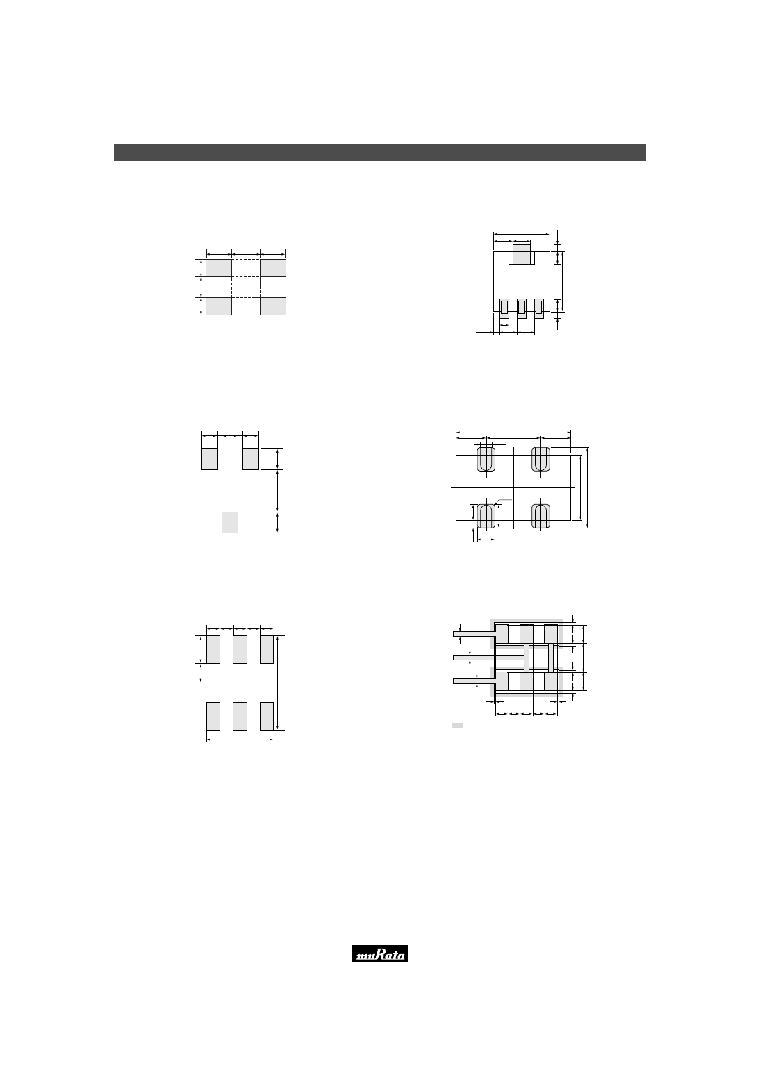
SMD Type CERAFIL
r
Standard Land Pattern Dimensions
26
9
!
Note
• Please read rating and
!
CAUTION (for storage and operating, rating, soldering and mounting, handling) in this catalog to prevent smoking and/or burning, etc.
• This catalog has only typical specifications because there is no space for detailed specifications. Therefore, please approve our product specification or transact the approval sheet for product specification before ordering.
■ CFXCD Series
(in mm)
1.8
2.0
1.8
1
.3
1
.6
1
.3
■ SFPCA Series
(in mm)
2.0
2.475
6.95
1
.6
1
.5
5
7
.4
5
0
.8
0
.9
0.925
2.0
2.0
1.1
■ CFUCG/CFUCF Series
(in mm)
1.2
0.7
0.7
1.4
1.2
2
.0
3
.5
2
.0
■ CFWCA Series
(in mm)
1.2
3.0
3.0
5.5
4-R3.0
11.5
7
.5
m
a
x
.
6
.5
2
.0
2
.1
1.8
0
.7
5
■ CFXCA Series
(in mm)
1.0
1
.5
2
.0
1.0
1.0
1.0
1.0
7
.0
5.0
■ SFECS Series
(1) : Input
(2) : Ground
(3) : Float (Signal Line)
(4) : Output
(in mm)
It shoes solder resist
land pattern.
(4)
(1)
(2)
(3)
0
.1
0
.1
1
.0
5
1
.4
0
0.1
0.1
0.6
0
.1
0
.1
1
.0
5
0
.3
0
.3
0
.3
0.8
0.8
0.6
0.8
Please read rating and
!
CAUTION (for storage and operating, rating, soldering and mounting, handling) in this PDF catalog to prevent smoking and/or burning, etc.
This catalog has only typical specifications. Therefore, you are requested to approve our product specification or to transact the approval sheet for product specificaion before ordering.
!
Note
P05E11.pdf 02.9.2
21
8
!
Note
• Please read rating and
!
CAUTION (for storage and operating, rating, soldering and mounting, handling) in this catalog to prevent smoking and/or burning, etc.
• This catalog has only typical specifications because there is no space for detailed specifications. Therefore, please approve our product specification or transact the approval sheet for product specification before ordering.
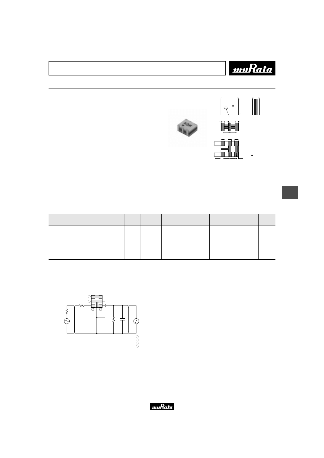
Ceramic Filters (CERAFILr)/Ceramic Discriminators for Communications Equipment
CERAFIL
r
MHz SMD Type SFECS10M8 Series
The SFECS10M8 series are small, high performance and
super thin (1.4mm) filters. Piezoelectric element is
connected in the sandwich shape by heat resistant
substrate.
The filters exhibit flat GDT characteristic in pass
band.
The filters are recommended for digital communication
applications and are perfect in hand held cellular
phones, pocket cordless phones, etc.
■ Features
1. The filters are mountable by automatic placers.
2. They are slim, at only 1.4mm thickness, and have
a small mounting area (3.5x3.1mm2) enabling
flexible PCB design.
3. Types with 10.7/10.75/10.8MHz of center
frequency are available.
4. Operating temperature range : -10 to +50 (degree C)
Storage temperature range : -40 to +85 (degree C)
Input electrode marker
3.45
±
0.2
3
.1
0
±
0
.2
1.4
±
0.1
(1)
(4)
(2)
(3)
0.7
±
0.3 0.7
±
0.3 0.7
±
0.3
(1.30) (1.30)
0
.8
5
±
0
.3
0
.8
5
±
0
.3
0~0.3
0~0.3
0.6
±
0.3
(1.35) (1.35)
0.6
±
0.3
0~0.3
0~0.3
0.4
+0.3
-0.2
(1) : Input
(2) : Ground
(3) : Float (Signal line)
(4) : Output
( ) : Reference
: EIAJ Monthly Code
(in mm)
Part Number
Nominal Center
Frequency (fn)
(MHz)
3dB
Bandwidth
(kHz)
Stop
Bandwidth
(kHz)
Insertion
Loss
(dB)
Ripple
(dB)
Spurious
Response
(dB)
GDT Deviation
(
µ
s)
Absolute GDT
(
µ
s)
Input/Output
Impedance
(ohm)
SFECS10M8PF00-R0
10.800
fn
±
110 min.
fn
±
310 max.
[within 20dB]
6.0 max.
[at fn]
0.5 max.
[within fn
±
100kHz]
-
1.5 max.
[within fn
±
100kHz]
2.8
±
1.0
µ
s
[at fn]
330
SFECS10M8RF00-R0
10.800
fn
±
135 min.
fn
±
350 max.
[within 20dB]
6.0 max.
[at fn]
0.5 max.
[within fn
±
100kHz]
-
1.2 max.
[within fn
±
100kHz]
2.6
±
1.0
µ
s
[at fn]
330
SFECS10M8SF00-R0
10.800
fn
±
150 min.
fn
±
420 max.
[within 20dB]
5.0 max.
[at fn]
1.0 max.
[within fn
±
110kHz]
25 min.
[within 9 to 12 MHz]
1.5 max.
[within fn
±
110kHz]
-
330
For safety purposes, connect the output of filters to the IF amplifier through a D.C. blocking capacitor. Avoid applying a direct current to the output of ceramic filters.
■ Test Circuit
Rg
S.S.G.
=−
10dBm
RF
Voltmeter
R2
1
2
3
C2
E2
E1
R1
: Input
: Ground
: Flout
: Output
1
2
3
4
4
Rg + R
1
= R
2
= Input/Output Impedance
C
2
= 10pF
Please read rating and
!
CAUTION (for storage and operating, rating, soldering and mounting, handling) in this PDF catalog to prevent smoking and/or burning, etc.
This catalog has only typical specifications. Therefore, you are requested to approve our product specification or to transact the approval sheet for product specificaion before ordering.
!
Note
P05E11.pdf 02.9.2
22
8
!
Note
• Please read rating and
!
CAUTION (for storage and operating, rating, soldering and mounting, handling) in this catalog to prevent smoking and/or burning, etc.
• This catalog has only typical specifications because there is no space for detailed specifications. Therefore, please approve our product specification or transact the approval sheet for product specification before ordering.
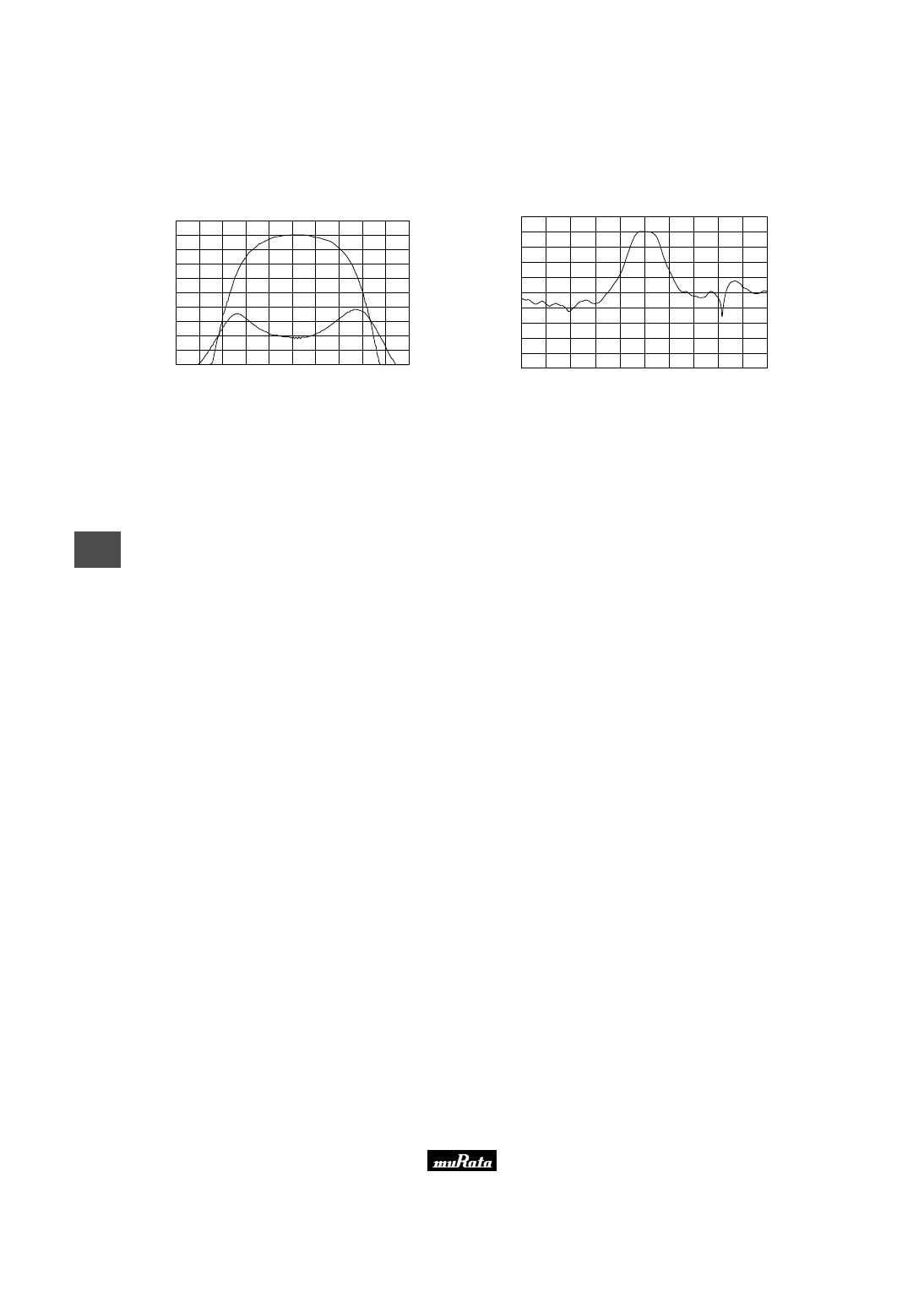
■ Frequency Characteristics
SFECS10M8PF00-R0
10.6
10.8
Frequency (MHz)
A
tt
e
n
u
a
ti
o
n
(
d
B
)
G
.
D
.
T
.
(
µ
s
e
c
)
8
6
4
2
0
6
2
3
4
5
7
10.7
10.9
11.0
SFECS10M8PF00-R0
A
tt
e
n
u
a
ti
o
n
(
d
B
)
40
20
0
80
60
9.6
10.2
Frequency (MHz)
12.0
10.8
11.4
Please read rating and
!
CAUTION (for storage and operating, rating, soldering and mounting, handling) in this PDF catalog to prevent smoking and/or burning, etc.
This catalog has only typical specifications. Therefore, you are requested to approve our product specification or to transact the approval sheet for product specificaion before ordering.
!
Note
P05E11.pdf 02.9.2
23
9
!
Note
• Please read rating and
!
CAUTION (for storage and operating, rating, soldering and mounting, handling) in this catalog to prevent smoking and/or burning, etc.
• This catalog has only typical specifications because there is no space for detailed specifications. Therefore, please approve our product specification or transact the approval sheet for product specification before ordering.
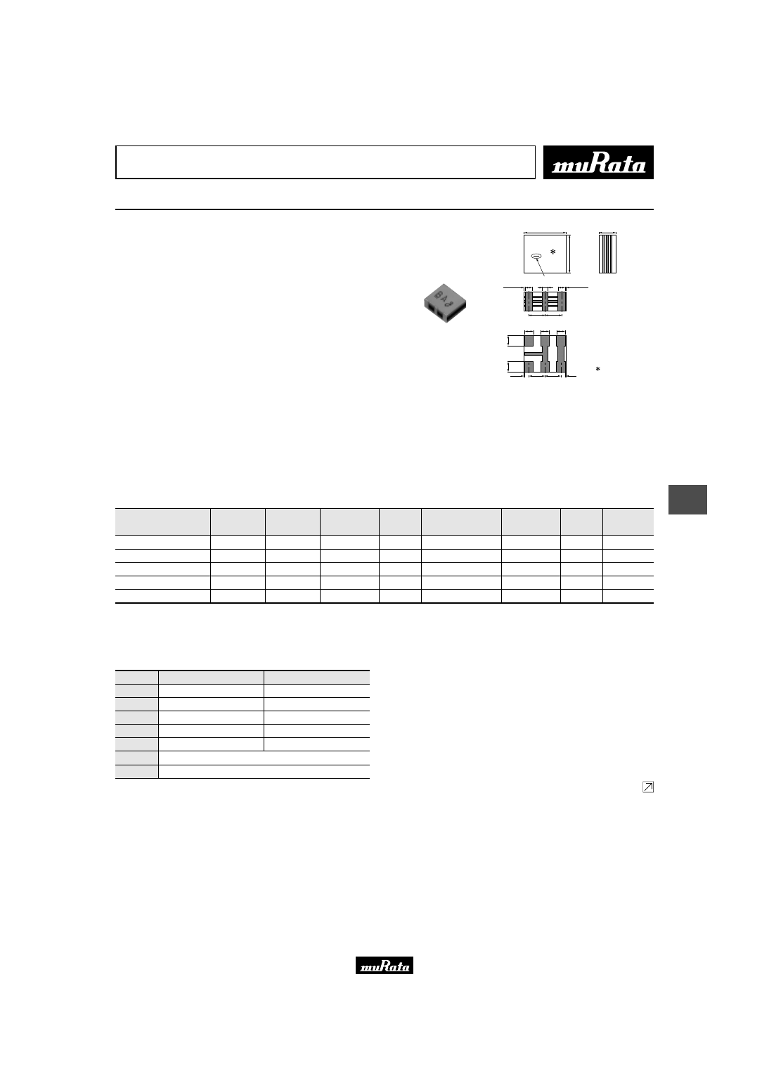
Ceramic Filters (CERAFILr)/Ceramic Discriminators for Communications Equipment
CERAFIL
r
MHz SMD Type SFECS10M7 Series
The SFECS10M7 series are small, high performance and
super thin (1.4mm) filters. Piezoelectric element is
connected in the sandwich shape by heat resistant
substrate.
The filters are recommended for digital communication
applications and are perfect in pocket cordless phones,
RKE (Remote Keyless Entry), TPMS (Tire Pressure
Monitoring System) etc.
■ Features
1. The filters are mountable by automatic placers.
2. They are slim, at only 1.4mm thickness, and have
a small mounting area (3.5x3.1mm2) enabling
flexible PCB design.
3. Various bandwidths are available. Select a
suitable type in accordance with the desires
selectivity.
4. Operating temperature range : -10 to +50 (degree C)
Storage temperature range : -40 to +85 (degree C)
Input electrode marker
3.45
±
0.2
3
.1
0
±
0
.2
1.4
±
0.1
(1)
(4)
(2)
(3)
0.7
±
0.3 0.7
±
0.3 0.7
±
0.3
(1.30) (1.30)
0
.8
5
±
0
.3
0
.8
5
±
0
.3
0~0.3
0~0.3
0.6
±
0.3
(1.35) (1.35)
0.6
±
0.3
0~0.3
0~0.3
0.4
+0.3
-0.2
(1) : Input
(2) : Ground
(3) : Float (Signal line)
(4) : Output
( ) : Reference
: EIAJ Monthly Code
(in mm)
Part Number
Center
Frequency (fo)
(MHz)
Nominal Center
Frequency(fn)
(MHz)
3dB Bandwidth
(kHz)
Attenuation
(kHz)
Insertion Loss
(at minimum loss point)
(dB)
Ripple
(within 3dB B.W.)
(dB)
Spurious
Attenuation
(dB)
Input/Output
Impedance
(ohm)
SFECS10M7HA00-R0
10.700
±
30kHz
-
180
±
40kHz
470 max.
4.5
±
2.0dB
1.0 max.
30 min.
330
SFECS10M7GA00-R0
10.700
±
30kHz
-
230
±
50kHz
510 max.
3.5
±
2.0dB
1.0 max.
30 min.
330
SFECS10M7FA00-R0
10.700
±
30kHz
-
280
±
50kHz
590 max.
3.0
±
2.0dB
1.0 max.
30 min.
330
SFECS10M7EA00-R0
10.700
±
30kHz
-
330
±
50kHz
700 max.
3.0
±
2.0dB
1.0 max.
30 min.
330
SFECS10M7DF0021-R0
-
10.700
fn
±
200kHz min.
950 max.
3.0
±
2.0dB
3.0 max.
20 min.
330
Area of Attenuation : [within 20dB] Area of Spurious Attenuation : [within 9MHz to 12MHz]
Center frequency (fo) defined by center of 3dB bandwidth.
■ Center Frequency Rank Code
CODE
D
B
A
C
E
Z
M
30kHz Step
10.64MHz
±
30kHz
10.67MHz
±
30kHz
10.70MHz
±
30kHz
10.73MHz
±
30kHz
10.76MHz
±
30kHz
25kHz Step
10.650MHz
±
25kHz
10.675MHz
±
25kHz
10.700MHz
±
25kHz
10.725MHz
±
25kHz
10.750MHz
±
25kHz
Combination A,B,C,D,E
Combination A,B,C
Continued on the following page.
Please read rating and
!
CAUTION (for storage and operating, rating, soldering and mounting, handling) in this PDF catalog to prevent smoking and/or burning, etc.
This catalog has only typical specifications. Therefore, you are requested to approve our product specification or to transact the approval sheet for product specificaion before ordering.
!
Note
P05E11.pdf 02.9.2
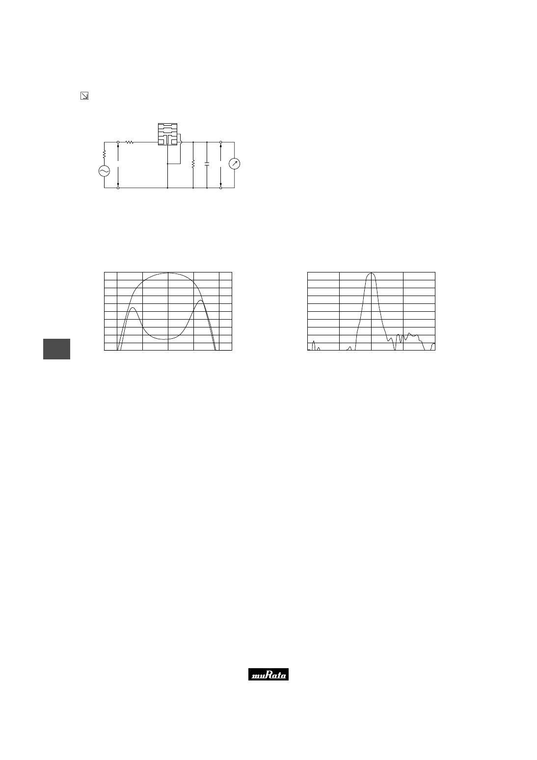
24
9
!
Note
• Please read rating and
!
CAUTION (for storage and operating, rating, soldering and mounting, handling) in this catalog to prevent smoking and/or burning, etc.
• This catalog has only typical specifications because there is no space for detailed specifications. Therefore, please approve our product specification or transact the approval sheet for product specification before ordering.
Continued from the preceding page.
■ Test Circuit
Rg=50
Ω
R1=280
Ω
R2=330
Ω
C2=10pF
(Including stray capacitance
and Input capacitance of RF Voltmeter)
RF
Voltmeter
E2
C2
E1
R2
R1
Rg
S.S.G.
=-10dBm
(4)
(1)
(2)
(3)
(1) : Input
(2) : Ground
(3) : Float
(4) : Output
■ Frequency Characteristics
SFECS10M7FA00-R0
A
tt
e
n
u
a
ti
o
n
(
d
B
)
G
.D
.T
.
(
µ
s
e
c
.)
Frequency (MHz)
0
2
4
6
8
10
4.60
4.40
4.20
4.00
3.80
3.60
3.40
3.20
3.00
2.80
2.60
10.500
10.600
10.700
10.800
10.900
SFECS10M7FA00-R0
A
tt
e
n
u
a
ti
o
n
(
d
B
)
Frequency (MHz)
0
10
20
30
40
50
8.700
9.700
10.700
11.700
12.700
Please read rating and
!
CAUTION (for storage and operating, rating, soldering and mounting, handling) in this PDF catalog to prevent smoking and/or burning, etc.
This catalog has only typical specifications. Therefore, you are requested to approve our product specification or to transact the approval sheet for product specificaion before ordering.
!
Note
P05E11.pdf 02.9.2
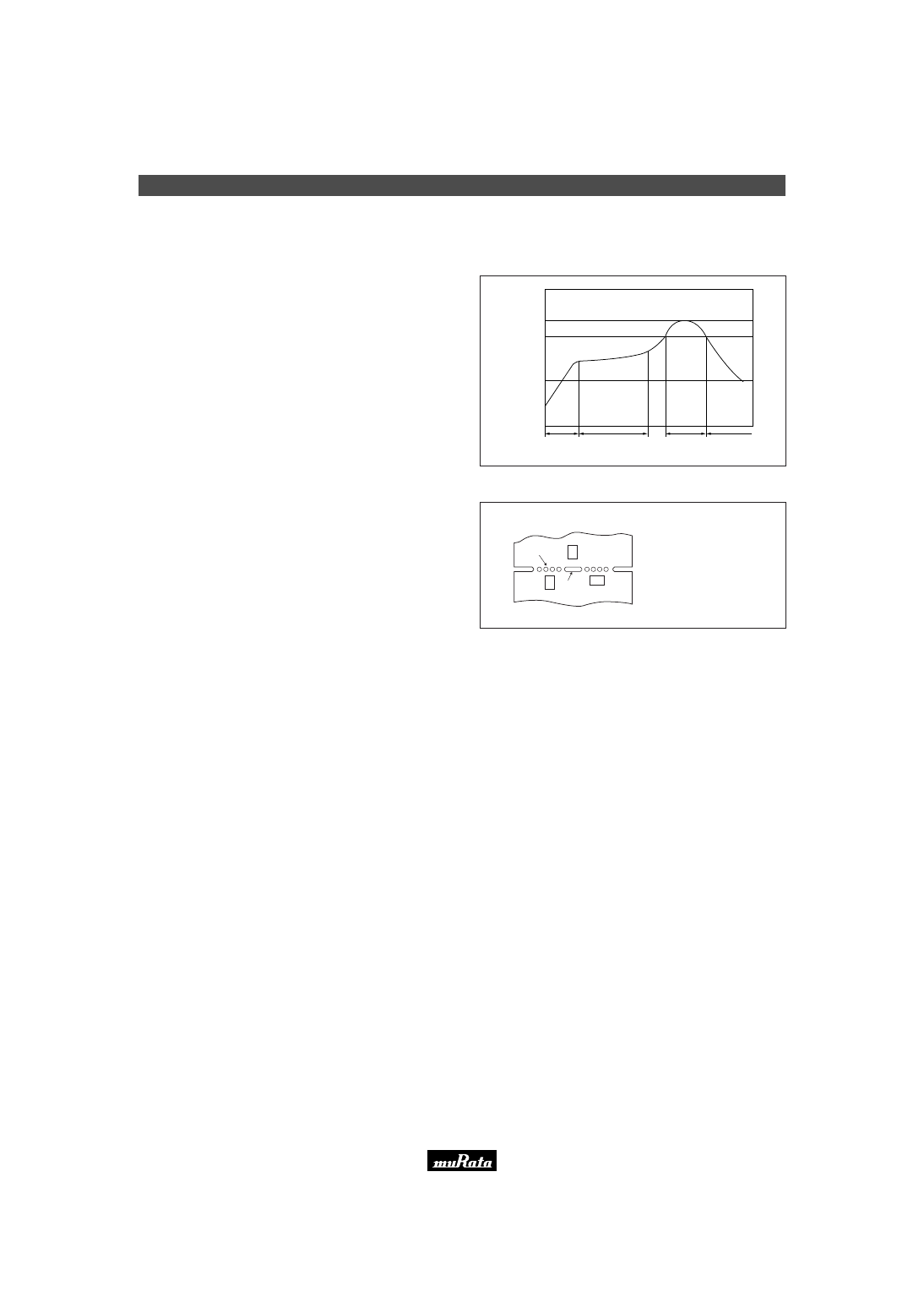
MHz SMD Type CERAFIL
r
Notice
25
9
!
Note
• Please read rating and
!
CAUTION (for storage and operating, rating, soldering and mounting, handling) in this catalog to prevent smoking and/or burning, etc.
• This catalog has only typical specifications because there is no space for detailed specifications. Therefore, please approve our product specification or transact the approval sheet for product specification before ordering.
■ Notice (Soldering and Mounting)
Filter is soldered twice within the following temperature
condition and then being placed in natural condition for
24 hours.
1. Standard Reflow Soldering Condition
(1) Reflow
The component cannot be withstand washing.
2. Wash
Filter is soldering at +280
±
5
°
C for 3
±
1 seconds and the
being placed in natural condition for 24 hours. The solder-
ing iron shall not touch the filter while soldering.
(2) Soldering Iron
+1
–0
Peak
(240
°
C max.)
Heating
(200
°
C)
Gradual
Cooling
Pre-heating
(120-170
°
C)
100
200
240
T
e
m
p
e
ra
tu
re
(
°
C
)
30sec. min. 60sec.-120sec.
30sec. max. 120sec. min.
■ Notice (Handling)
1. The component will be damaged when an excessive
stress is applied.
2. The component may be damaged if excess mechanical
stress is applied to it mounted on the printed circuit
board.
3. Design layout of components on the PC board to
minimize the stress imposed on the warp or flexure of the
board.
4. After installing chips, if solder is excessively applied to
the circuit board, mechanical stress will cause destruction
resistance characteristics to lower. To prevent this, be
extremly careful in determining shape and dimension
before designing the circuit board diagram.
5. When the positioning claws and pick up nozzle are worn,
the load is applied to the chip while positioning is
concentrated to one positioning accuracy, etc. Careful
checking and maintenance are necessary to prevent
unexpected trouble.
6. When correcting chips with a soldering iron, the tip of the
soldering iron should not directly touch the chip
component. Depending on the soldering conditions, the
effective area of terminations may be reduced. The use
of solder containing Ag should be done to prevent the
electrode erosion.
7. Do not clean or wash the component as it is not
hermetically sealed.
8. In case of covering discriminator with over coat,
conditions such as material of resin, cure temperature,
and so on should be evaluated well.
9. Do not use strong acidity flux, more than 0.2wt% chlorine
content, in re-flow soldering.
10. Accurate test circuit values are required to measure
electrical characteristics.
It may be a cause of mis-correlation if there is any
deviation, especially stray capacitance, from the test
circuit in the specification.
[Component layout close to board]
Susceptibility to
stress is in the order
of; A>C>B
B
A
C
Slit
Perforation
Please read rating and
!
CAUTION (for storage and operating, rating, soldering and mounting, handling) in this PDF catalog to prevent smoking and/or burning, etc.
This catalog has only typical specifications. Therefore, you are requested to approve our product specification or to transact the approval sheet for product specificaion before ordering.
!
Note
P05E11.pdf 02.9.2

SMD Type CERAFIL
r
Standard Land Pattern Dimensions
26
9
!
Note
• Please read rating and
!
CAUTION (for storage and operating, rating, soldering and mounting, handling) in this catalog to prevent smoking and/or burning, etc.
• This catalog has only typical specifications because there is no space for detailed specifications. Therefore, please approve our product specification or transact the approval sheet for product specification before ordering.
■ CFXCD Series
(in mm)
1.8
2.0
1.8
1
.3
1
.6
1
.3
■ SFPCA Series
(in mm)
2.0
2.475
6.95
1
.6
1
.5
5
7
.4
5
0
.8
0
.9
0.925
2.0
2.0
1.1
■ CFUCG/CFUCF Series
(in mm)
1.2
0.7
0.7
1.4
1.2
2
.0
3
.5
2
.0
■ CFWCA Series
(in mm)
1.2
3.0
3.0
5.5
4-R3.0
11.5
7
.5
m
a
x
.
6
.5
2
.0
2
.1
1.8
0
.7
5
■ CFXCA Series
(in mm)
1.0
1
.5
2
.0
1.0
1.0
1.0
1.0
7
.0
5.0
■ SFECS Series
(1) : Input
(2) : Ground
(3) : Float (Signal Line)
(4) : Output
(in mm)
It shoes solder resist
land pattern.
(4)
(1)
(2)
(3)
0
.1
0
.1
1
.0
5
1
.4
0
0.1
0.1
0.6
0
.1
0
.1
1
.0
5
0
.3
0
.3
0
.3
0.8
0.8
0.6
0.8
Please read rating and
!
CAUTION (for storage and operating, rating, soldering and mounting, handling) in this PDF catalog to prevent smoking and/or burning, etc.
This catalog has only typical specifications. Therefore, you are requested to approve our product specification or to transact the approval sheet for product specificaion before ordering.
!
Note
P05E11.pdf 02.9.2
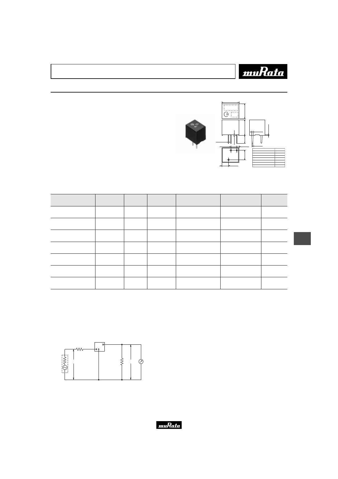
31
10
!
Note
• Please read rating and
!
CAUTION (for storage and operating, rating, soldering and mounting, handling) in this catalog to prevent smoking and/or burning, etc.
• This catalog has only typical specifications because there is no space for detailed specifications. Therefore, please approve our product specification or transact the approval sheet for product specification before ordering.
Ceramic Filters (CERAFILr)/Ceramic Discriminators for Communications Equipment
CERAFIL
r
Plastic Case General Use CFULA_A Series
CFULA_A series are high selectivity ceramic filters,
which consist of 4 ceramic elements connected in a
ladder form.
Most suitable for digital communications and cellular
phones because of their improved GDT characteristics.
■ Features
1. High selectivity.
2. A variety of bandwidth available.
3. Excellent GDT characteristics are available within
pass bandwidth.
4. Easily mounted on a printed circuit board
5. Operating temperature range : -20 to +80 (degree C)
Storage temperature range : -40 to +85 (degree C)
3
.0
±
0
.3
7
.0
±
0
.3
4
.2
±
0
.3
7
.3
±
0
.3
0.8
±
0.1
0.6
±
0.1
1.2
±
0.5
8.0
±
0.3
3.3
±
0.5
2.7
±
0.3
(1)
(2)
(3)
0
.3
±
0
.1
1
.5
m
a
x
.
0.15
±
0.05
Connection
(1) : Input
(2) : Ground
(3) : Output
(in mm)
Type
CFULA455KB2A-B0
CFULA455KC2A-B0
CFULA455KD4A-B0
CFULA455KE4A-B0
CFULA455KF4A-B0
CFULA455KG1A-B0
CFULA455KH1A-B0
Marking
B
C
D
E
F
G
HT
MARKING
EIAJ
CODE
Part Number
Center
Frequency (fo)
(kHz)
6dB
Bandwidth
(kHz)
Stop
Bandwidth
(kHz)
Stop Band
Attenuation
(dB)
Insertion
Loss
(dB)
Input/Output
Impedance
(ohm)
CFULA455KB2A-B0
455.0
±
2.0kHz
fn
±
15.0
min.
fn
±
30.0 max.
[within 40dB]
27 min.
[within fn
±
100kHz]
4.0 max.
[at minimum loss point]
1500
CFULA455KC2A-B0
455.0
±
2.0kHz
fn
±
12.5
min.
fn
±
24.0 max.
[within 40dB]
27 min.
[within fn
±
100kHz]
4.0 max.
[at minimum loss point]
1500
CFULA455KD4A-B0
455.0
±
1.5kHz
fn
±
10.0
min.
fn
±
20.0 max.
[within 40dB]
27 min.
[within fn
±
100kHz]
4.0 max.
[at minimum loss point]
1500
CFULA455KE4A-B0
455.0
±
1.5kHz
fn
±
7.5
min.
fn
±
15.0 max.
[within 40dB]
27 min.
[within fn
±
100kHz]
6.0 max.
[at minimum loss point]
1500
CFULA455KF4A-B0
455.0
±
1.5kHz
fn
±
6.0
min.
fn
±
12.5 max.
[within 40dB]
27 min.
[within fn
±
100kHz]
6.0 max.
[at minimum loss point]
2000
CFULA455KG1A-B0
455.0
±
1.0kHz
fn
±
4.5
min.
fn
±
10.0 max.
[within 40dB]
25 min.
[within fn
±
100kHz]
6.0 max.
[at minimum loss point]
2000
CFULA455KH1A-B0
455.0
±
1.0kHz
fn
±
3.0
min.
fn
±
9.0 max.
[within 40dB]
35 min.
[within fn
±
100kHz]
6.0 max.
[at minimum loss point]
2000
For safety purposes, connect the output of filters to the IF amplifier through a D.C. blocking capacitor. Avoid applying a direct current to the output of ceramic filters.
(fn) means nominal center frequency 455kHz.
The order quantity should be an integral multiple of the "Minimum Quantity" shown in package page in this catalog.
■ Test Circuit
E1
R1
Rg
S.S.G.
0dBm
R2
E2
RF Voltmeter
Connection
(1) : Input
(2) : Ground
(3) : Output
(1) (2)
(3)
Rg+R1=R2=Input/Output Impedance
Please read rating and
!
CAUTION (for storage and operating, rating, soldering and mounting, handling) in this PDF catalog to prevent smoking and/or burning, etc.
This catalog has only typical specifications. Therefore, you are requested to approve our product specification or to transact the approval sheet for product specificaion before ordering.
!
Note
P05E11.pdf 02.9.2
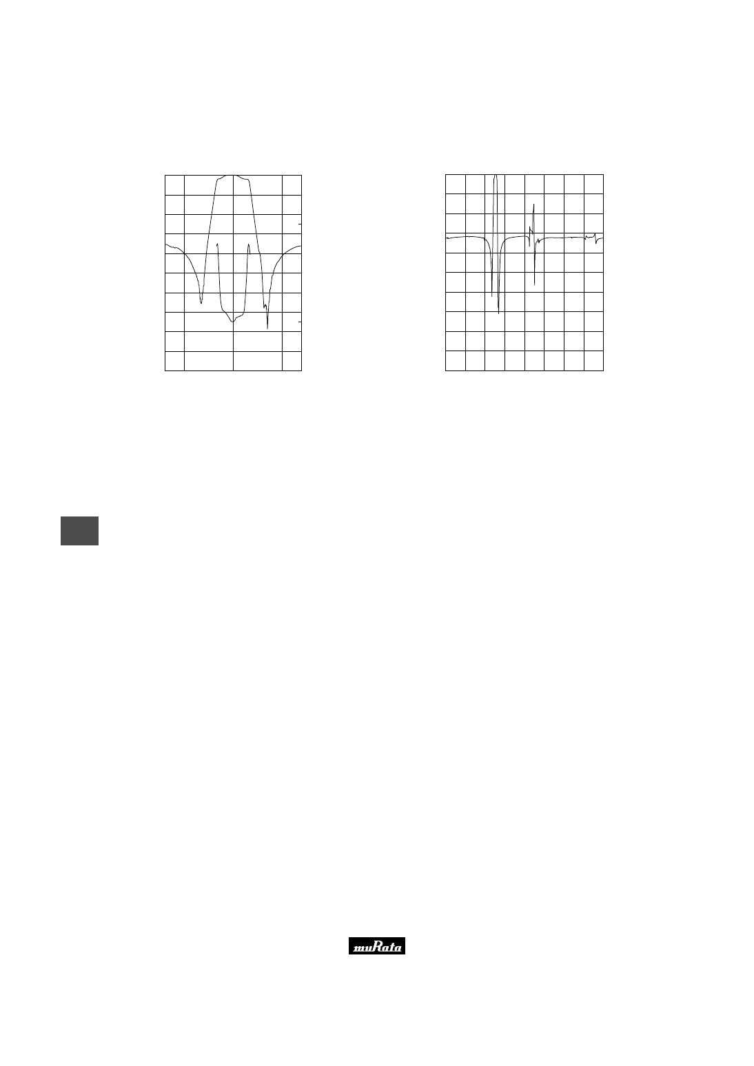
32
10
!
Note
• Please read rating and
!
CAUTION (for storage and operating, rating, soldering and mounting, handling) in this catalog to prevent smoking and/or burning, etc.
• This catalog has only typical specifications because there is no space for detailed specifications. Therefore, please approve our product specification or transact the approval sheet for product specification before ordering.
■ Frequency Characteristics
CFULA455KE4A-B0
100
40
30
20
10
0
A
tt
e
n
u
a
ti
o
n
(
d
B
)
0
50
100
150
200
G
.D
.T
.
(
µ
s
e
c
.)
430
455
480
Frequency (kHz)
90
80
70
60
50
CFULA455KE4A-B0
100
40
30
20
10
0
A
tt
e
n
u
a
ti
o
n
(
d
B
)
200
Frequency (kHz)
90
80
70
60
50
300
400
500
600
700
800
900
1000
Please read rating and
!
CAUTION (for storage and operating, rating, soldering and mounting, handling) in this PDF catalog to prevent smoking and/or burning, etc.
This catalog has only typical specifications. Therefore, you are requested to approve our product specification or to transact the approval sheet for product specificaion before ordering.
!
Note
P05E11.pdf 02.9.2
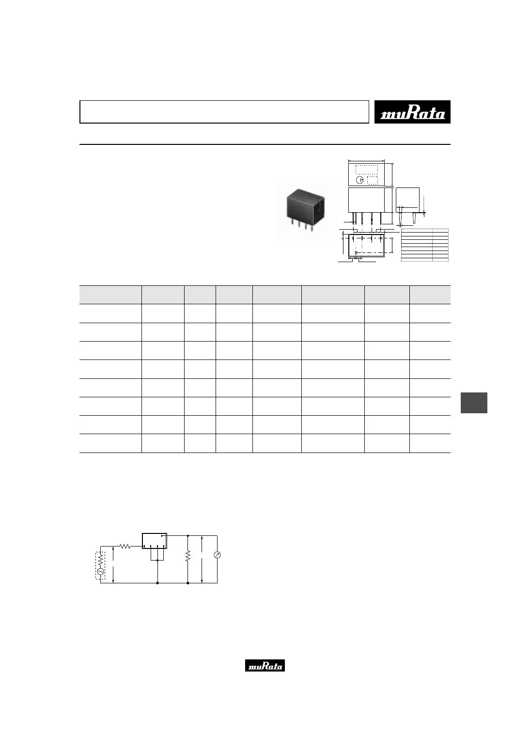
33
11
!
Note
• Please read rating and
!
CAUTION (for storage and operating, rating, soldering and mounting, handling) in this catalog to prevent smoking and/or burning, etc.
• This catalog has only typical specifications because there is no space for detailed specifications. Therefore, please approve our product specification or transact the approval sheet for product specification before ordering.
Ceramic Filters (CERAFILr)/Ceramic Discriminators for Communications Equipment
CERAFIL
r
Plastic Case Miniaturized Type CFWLA_A Series
Ceramic filter CFWLA_A series are low profile high
selectivity ceramic filters which use 6 elements in
ladder form.
They are best suitable to high-class transceivers,
cordless telephones and amateur radios.
■ Features
1. Low profile, high selectivity.
2. Available bandwidths are B to J as standard.
3. Easily mountable on any PC board.
4. Operating temperature range : -20 to +80 (degree C)
Storage temperature range : -40 to +85 (degree C)
4
.3
±
0
.3
0.15
1
.5
m
a
x
.
2.3
±
0.5
2.0
±
0.3
2.9
±
0.3
11.0
±
0.5
1.2
±
0.5
(1)
(2)
(4) (3)
(5)
1
.3
5
±
0
.5
7
.0
±
0
.5
3.
5
±
0.
5
0.6
±
0.1
0.8
±
0.1
7
.5
±
0
.5
2.6
±
0.3
Connection
(1) : Input
(2)
(3) : Ground
(4)
(5) : Output
(in mm)
2.9
2.9—
—0.3
0.3
2.9
±
0.3
Type
CFWLA455KBFA-B0
CFWLA455KCFA-B0
CFWLA455KDFA-B0
CFWLA455KEFA-B0
CFWLA455KFFA-B0
CFWLA455KGFA-B0
CFWLA455KHFA-B0
CFWLA455KJFA-B0
Marking
B
C
D
E
F
G
HT
IT
}
MARKING
EIAJ
CODE
Part Number
Nominal Center
Frequency (fn)
(kHz)
6dB
Bandwidth
(kHz)
Stop
Bandwidth
(kHz)
Stop Band
Attenuation
(dB)
Insertion
Loss
(dB)
Ripple
(dB)
Input/Output
Impedance
(ohm)
CFWLA455KBFA-B0
455
fn
±
15.0
min.
fn
±
30.0 max.
[within 50dB]
35 min.
[within fn
±
100kHz]
4.0 max.
[at minimum loss point]
3.0 max.
[within fn
±
10kHz]
1500
CFWLA455KCFA-B0
455
fn
±
12.5
min.
fn
±
24.0 max.
[within 50dB]
35 min.
[within fn
±
100kHz]
4.0 max.
[at minimum loss point]
3.0 max.
[within fn
±
8kHz]
1500
CFWLA455KDFA-B0
455
fn
±
10.0
min.
fn
±
20.0 max.
[within 50dB]
35 min.
[within fn
±
100kHz]
4.0 max.
[at minimum loss point]
3.0 max.
[within fn
±
7kHz]
1500
CFWLA455KEFA-B0
455
fn
±
7.5
min.
fn
±
15.0 max.
[within 50dB]
35 min.
[within fn
±
100kHz]
6.0 max.
[at minimum loss point]
3.0 max.
[within fn
±
5kHz]
1500
CFWLA455KFFA-B0
455
fn
±
6.0
min.
fn
±
12.5 max.
[within 50dB]
35 min.
[within fn
±
100kHz]
6.0 max.
[at minimum loss point]
3.0 max.
[within fn
±
4kHz]
2000
CFWLA455KGFA-B0
455
fn
±
4.5
min.
fn
±
10.0 max.
[within 50dB]
35 min.
[within fn
±
100kHz]
6.0 max.
[at minimum loss point]
2.0 max.
[within fn
±
3kHz]
2000
CFWLA455KHFA-B0
455
fn
±
3.0
min.
fn
±
9.0 max.
[within 50dB]
60 min.
[within fn
±
100kHz]
6.0 max.
[at minimum loss point]
2.0 max.
[within fn
±
2kHz]
2000
CFWLA455KJFA-B0
455
fn
±
2.0
min.
fn
±
7.5 max.
[within 50dB]
60 min.
[within fn
±
100kHz]
7.0 max.
[at minimum loss point]
2.0 max.
[within fn
±
1.5kHz]
2000
For safety purposes, connect the output of filters to the IF amplifier through a D.C. blocking capacitor. Avoid applying a direct current to the output of ceramic filters.
The order quantity should be an integral multiple of the "Minimum Quantity" shown in package page in this catalog.
■ Test Circuit
E1
R1
R2
E2
RF Voltmeter
Connection
(1) : Input
(5) : Output
(2)(3)(4) : Ground
Rg
S.S.G.
0dBm
(1) (2) (3) (4)
(5)
Rg+R1=R2=Input/Output Impedance
Please read rating and
!
CAUTION (for storage and operating, rating, soldering and mounting, handling) in this PDF catalog to prevent smoking and/or burning, etc.
This catalog has only typical specifications. Therefore, you are requested to approve our product specification or to transact the approval sheet for product specificaion before ordering.
!
Note
P05E11.pdf 02.9.2
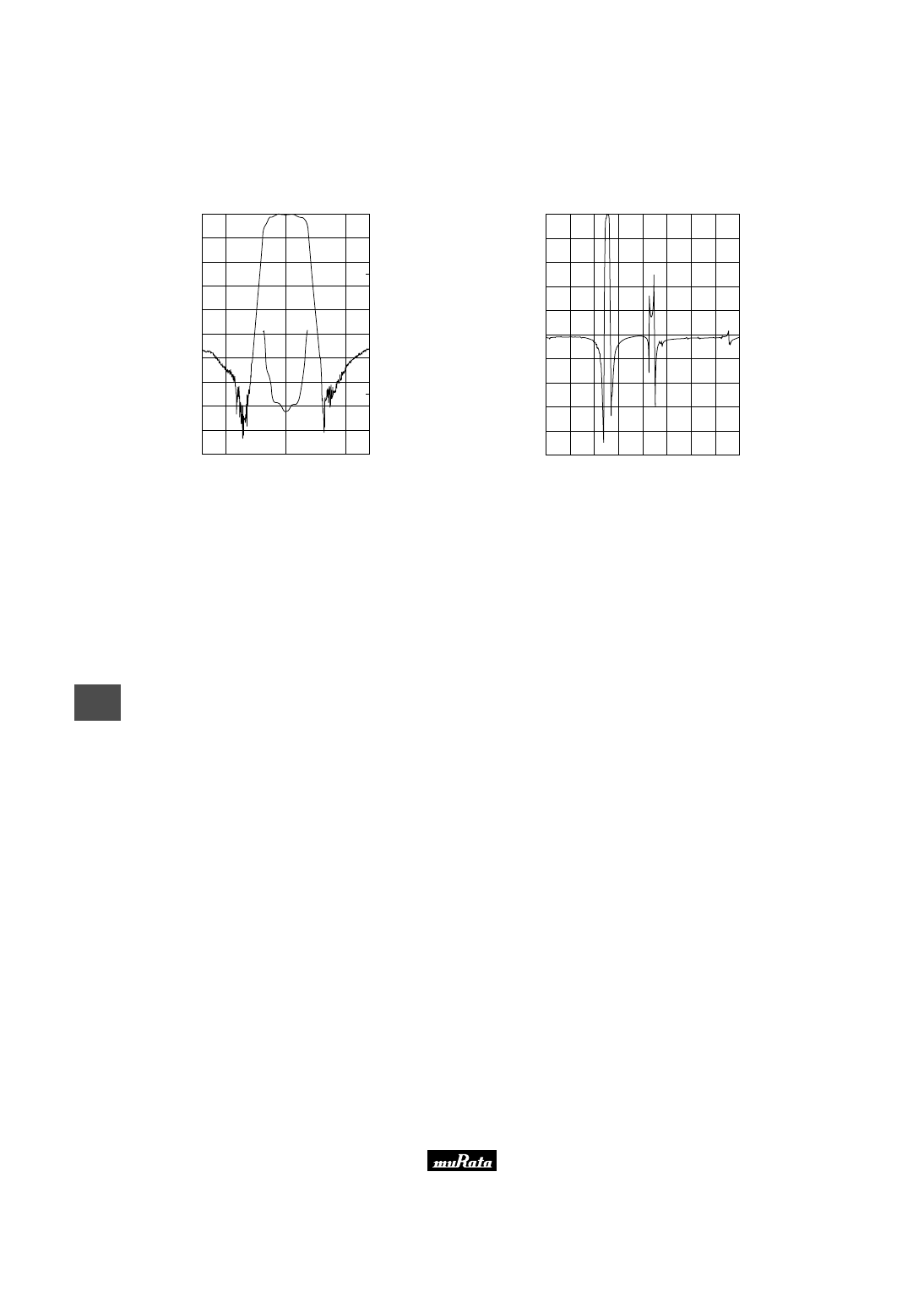
34
11
!
Note
• Please read rating and
!
CAUTION (for storage and operating, rating, soldering and mounting, handling) in this catalog to prevent smoking and/or burning, etc.
• This catalog has only typical specifications because there is no space for detailed specifications. Therefore, please approve our product specification or transact the approval sheet for product specification before ordering.
■ Frequency Characteristics
CFWLA455KEFA-B0
100
40
30
20
10
0
A
tt
e
n
u
a
ti
o
n
(
d
B
)
0
100
200
300
400
G
.D
.T
.
(
µ
s
e
c
.)
430
455
480
Frequency (kHz)
90
80
70
60
50
CFWLA455KEFA-B0
100
40
30
20
10
0
A
tt
e
n
u
a
ti
o
n
(
d
B
)
200
Frequency (kHz)
90
80
70
60
50
300
400
500
600
700
800
900
1000
Please read rating and
!
CAUTION (for storage and operating, rating, soldering and mounting, handling) in this PDF catalog to prevent smoking and/or burning, etc.
This catalog has only typical specifications. Therefore, you are requested to approve our product specification or to transact the approval sheet for product specificaion before ordering.
!
Note
P05E11.pdf 02.9.2
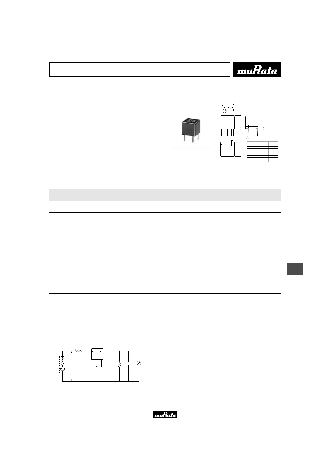
35
12
!
Note
• Please read rating and
!
CAUTION (for storage and operating, rating, soldering and mounting, handling) in this catalog to prevent smoking and/or burning, etc.
• This catalog has only typical specifications because there is no space for detailed specifications. Therefore, please approve our product specification or transact the approval sheet for product specification before ordering.
Ceramic Filters (CERAFILr)/Ceramic Discriminators for Communications Equipment
CERAFIL
r
Plastic Case Miniaturized Type CFULB_A Series
CFULB_A series ceramic filters are miniature, high
performance ceramic filters composed of piezoelectric
elements connected in a ladder form.
These filters, with only 6.3mm high, are 65% the
volume of conventional types. (CFULA455K_A series)
They are well suited for miniaturizing various kinds
of communications equipment, pocket pagers, car
radios, cordless telephones and mobile telephones.
■ Features
1. Miniature and high selectivity.
2. A variety of bandwidths are available.
3. Operating temperature range : -20 to +80 (degree C)
Storage temperature range : -40 to +85 (degree C)
4
.3
±
0
.3
1
.0
m
a
x
.
1.8
±
0.3
2.4
±
0.3
6.5
±
0.3
0.8
±
0.3
1.
0
±
0.
3
6
.3
±
0
.3
6
.5
±
0
.3
0.5
±
0.1
0.7
±
0.1
3
.5
±
0
.3
0.7
±
0.3
(1)
(2)
(3)
(4)
0.15
±
0.05
Connection
(1) : Input
(2) : Output
(3)
: Ground
(4)
(in mm)
Type
CFULB455KB2A-B0
CFULB455KC2A-B0
CFULB455KD4A-B0
CFULB455KE4A-B0
CFULB455KF4A-B0
CFULB455KG1A-B0
CFULB455KH1A-B0
CFULB455KJ1A-B0
Marking
55B
55C
55D
55E
55F
55G
55H
55I
}
MARKING
EIAJ
CODE
Part Number
Center
Frequency (fo)
(kHz)
6dB
Bandwidth
(kHz)
Stop
Bandwidth
(kHz)
Stop Band
Attenuation
(dB)
Insertion
Loss
(dB)
Input/Output
Impedance
(ohm)
CFULB455KB2A-B0
455.0
±
2.0kHz
fn
±
15.0
min.
fn
±
30.0 max.
[within 40dB]
27 min.
[within fn
±
100kHz]
4.0 max.
[at minimum loss point]
1500
CFULB455KC2A-B0
455.0
±
2.0kHz
fn
±
12.5
min.
fn
±
24.0 max.
[within 40dB]
27 min.
[within fn
±
100kHz]
4.0 max.
[at minimum loss point]
1500
CFULB455KD4A-B0
455.0
±
1.5kHz
fn
±
10.0
min.
fn
±
20.0 max.
[within 40dB]
27 min.
[within fn
±
100kHz]
4.0 max.
[at minimum loss point]
1500
CFULB455KE4A-B0
455.0
±
1.5kHz
fn
±
7.5
min.
fn
±
15.0 max.
[within 40dB]
27 min.
[within fn
±
100kHz]
6.0 max.
[at minimum loss point]
1500
CFULB455KF4A-B0
455.0
±
1.5kHz
fn
±
6.0
min.
fn
±
12.5 max.
[within 40dB]
27 min.
[within fn
±
100kHz]
6.0 max.
[at minimum loss point]
2000
CFULB455KG1A-B0
455.0
±
1.0kHz
fn
±
4.5
min.
fn
±
10.0 max.
[within 40dB]
25 min.
[within fn
±
100kHz]
6.0 max.
[at minimum loss point]
2000
CFULB455KH1A-B0
455.0
±
1.0kHz
fn
±
3.0
min.
fn
±
9.0 max.
[within 40dB]
35 min.
[within fn
±
100kHz]
6.0 max.
[at minimum loss point]
2000
CFULB455KJ1A-B0
455.0
±
1.0kHz
fn
±
2.0
min.
fn
±
7.5 max.
[within 40dB]
35 min.
[within fn
±
100kHz]
6.0 max.
[at minimum loss point]
2000
For safety purposes, connect the output of filters to the IF amplifier through a D.C. blocking capacitor. Avoid applying a direct current to the output of ceramic filters.
(fn) means nominal center frequency 455kHz.
The order quantity should be an integral multiple of the "Minimum Quantity" shown in package page in this catalog.
■ Test Circuit
E1
R1
Rg
S.S.G.
0dBm
R2
E2
RF Voltmeter
Connection
(1) : Input
(2) : Output
(3)(4) :Ground
(1)
(2)
(3)
(4)
Rg+R1=R2=Input/Output Impedance
Please read rating and
!
CAUTION (for storage and operating, rating, soldering and mounting, handling) in this PDF catalog to prevent smoking and/or burning, etc.
This catalog has only typical specifications. Therefore, you are requested to approve our product specification or to transact the approval sheet for product specificaion before ordering.
!
Note
P05E11.pdf 02.9.2
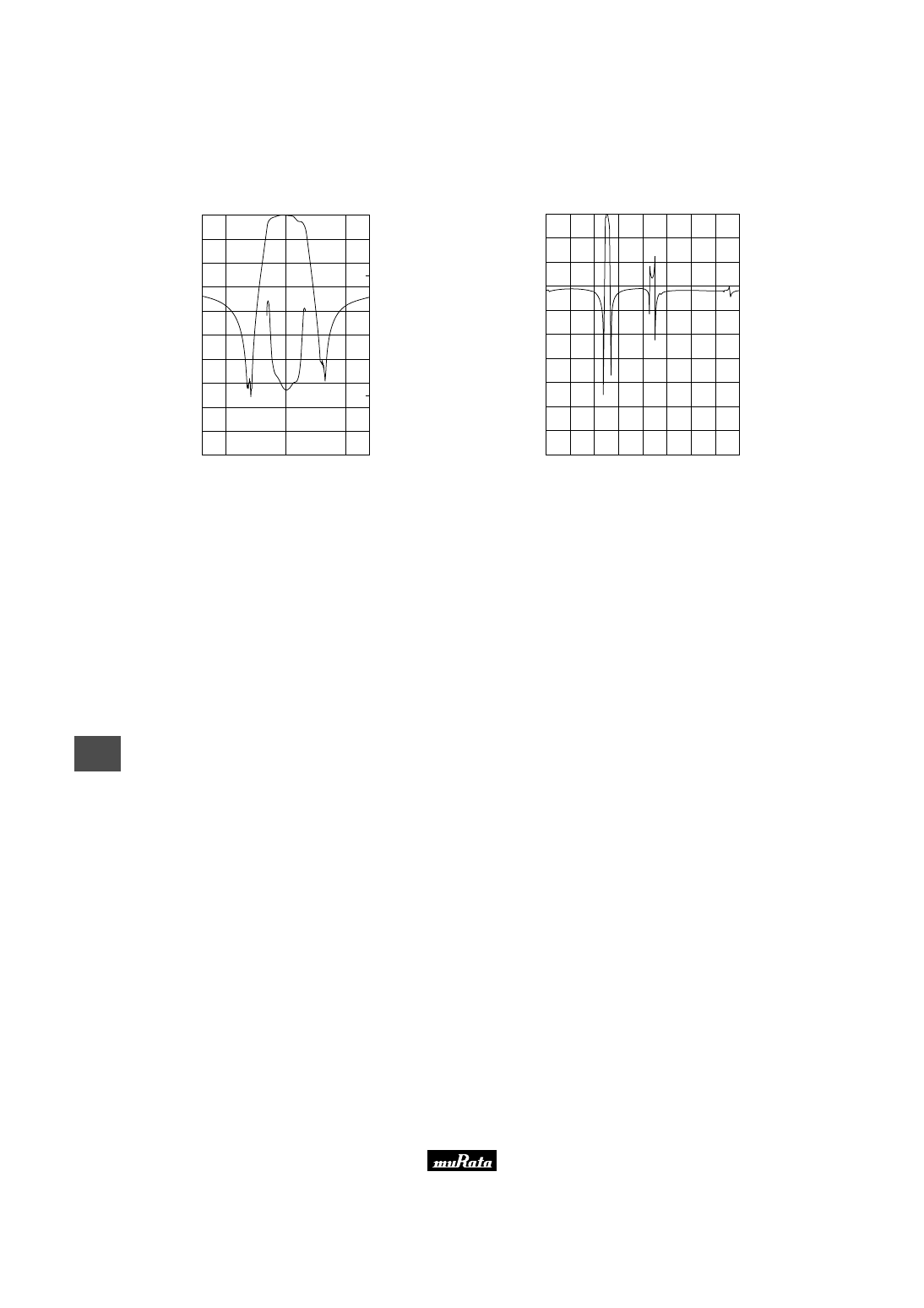
36
12
!
Note
• Please read rating and
!
CAUTION (for storage and operating, rating, soldering and mounting, handling) in this catalog to prevent smoking and/or burning, etc.
• This catalog has only typical specifications because there is no space for detailed specifications. Therefore, please approve our product specification or transact the approval sheet for product specification before ordering.
■ Frequency Characteristics
CFULB455KE4A-B0
100
40
30
20
10
0
A
tt
e
n
u
a
ti
o
n
(
d
B
)
0
50
100
150
200
G
.D
.T
.
(
µ
s
e
c
.)
430
455
480
Frequency (kHz)
90
80
70
60
50
CFULB455KE4A-B0
100
40
30
20
10
0
A
tt
e
n
u
a
ti
o
n
(
d
B
)
200
Frequency (kHz)
90
80
70
60
50
300
400
500
600
700
800
900
1000
Please read rating and
!
CAUTION (for storage and operating, rating, soldering and mounting, handling) in this PDF catalog to prevent smoking and/or burning, etc.
This catalog has only typical specifications. Therefore, you are requested to approve our product specification or to transact the approval sheet for product specificaion before ordering.
!
Note
P05E11.pdf 02.9.2
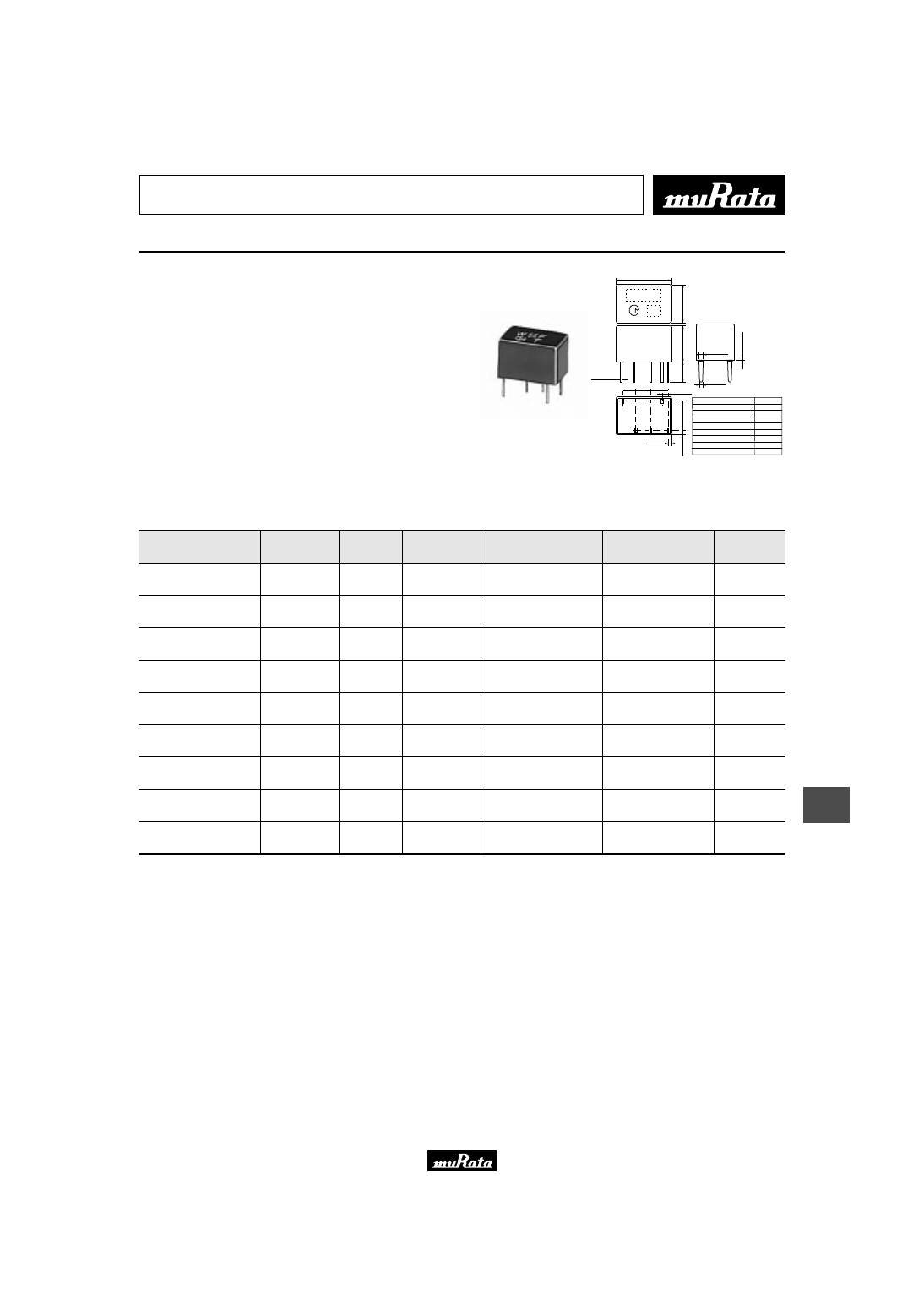
37
13
!
Note
• Please read rating and
!
CAUTION (for storage and operating, rating, soldering and mounting, handling) in this catalog to prevent smoking and/or burning, etc.
• This catalog has only typical specifications because there is no space for detailed specifications. Therefore, please approve our product specification or transact the approval sheet for product specification before ordering.
Ceramic Filters (CERAFILr)/Ceramic Discriminators for Communications Equipment
CERAFIL
r
Plastic Case General Use CFWLB_A Series
CFWLB_A series ceramic filters are miniature, high
performance ceramic filters composed of piezoelectric
elements connected in a ladder form.
These filters, with only 6.3mm high, are 67% the
volume of conventional types. (CFWLB_A series)
They are well suited for miniaturizing various kinds
of communications equipment, pocket pagers, pagers,
car radios, cordless telephones and mobile telephones.
■ Features
1. Miniature and high selectivity.
2. A variety of bandwidths are available.
3. Operating temperature range : -20 to +80 (degree C)
Storage temperature range : -40 to +85 (degree C)
4
.3
±
0
.3
1
.0
m
a
x
.
2.7
±
0.3
2.5
±
0.3
9.5
±
0.3
0.7
±
0.3
1
.0
±
0
.3
6
.3
±
0
.3
6
.5
±
0
.3
0.5
±
0.1
0.7
±
0.1
3
.5
±
0
.3
0.9
±
0.3
0.15
±
0.05
(1)
(3)
(4)
(2)
(5)
2.8
±
0.3
Type
CFWLB455KBFA-B0
CFWLB455KCFA-B0
CFWLB455KDFA-B0
CFWLB455KEFA-B0
CFWLB455KFFA-B0
CFWLB455KGFA-B0
CFWLB455KHFA-B0
CFWLB455KJFA-B0
Marking
W55B
W55C
W55D
W55E
W55F
W55G
W55H
W55I
Connection
(1) : Input
(2) : Output
(3)
(4) : Ground
(5)
(in mm)
}
MARKING
EIAJ
CODE
Part Number
Nominal Center
Frequency (fn)
(kHz)
6dB
Bandwidth
(kHz)
Stop
Bandwidth
(kHz)
Stop Band
Attenuation
(dB)
Insertion
Loss
(dB)
Input/Output
Impedance
(ohm)
CFWLB455KBFA-B0
455
fn
±
15.0
min.
fn
±
30.0 max.
[within 50dB]
35 min.
[within fn
±
100kHz]
4.0 max.
[at minimum loss point]
1500
CFWLB455KCFA-B0
455
fn
±
12.5
min.
fn
±
24.0 max.
[within 50dB]
35 min.
[within fn
±
100kHz]
4.0 max.
[at minimum loss point]
1500
CFWLB455KDFA-B0
455
fn
±
10.0
min.
fn
±
20.0 max.
[within 50dB]
35 min.
[within fn
±
100kHz]
4.0 max.
[at minimum loss point]
1500
CFWLB455KEFA-B0
455
fn
±
7.5
min.
fn
±
15.0 max.
[within 50dB]
35 min.
[within fn
±
100kHz]
6.0 max.
[at minimum loss point]
1500
CFWLB455KEFA004-B0
455
fn
±
7.5
min.
fn
±
15.0 max.
[within 60dB]
60 min.
[within fn
±
15kHz to 30kHz]
5.0 max.
[at fn]
1500
CFWLB455KFFA-B0
455
fn
±
6.0
min.
fn
±
12.5 max.
[within 50dB]
35 min.
[within fn
±
100kHz]
6.0 max.
[at minimum loss point]
2000
CFWLB455KGFA-B0
455
fn
±
4.5
min.
fn
±
10.0 max.
[within 50dB]
35 min.
[within fn
±
100kHz]
6.0 max.
[at minimum loss point]
2000
CFWLB455KHFA-B0
455
fn
±
3.0
min.
fn
±
9.0 max.
[within 50dB]
55 min.
[within fn
±
100kHz]
6.0 max.
[at minimum loss point]
2000
CFWLB455KJFA-B0
455
fn
±
2.0
min.
fn
±
7.0 max.
[within 50dB]
55 min.
[within fn
±
100kHz]
7.0 max.
[at minimum loss point]
2000
For safety purposes, connect the output of filters to the IF amplifier through a D.C. blocking capacitor. Avoid applying a direct current to the output of ceramic filters.
The order quantity should be an integral multiple of the "Minimum Quantity" shown in package page in this catalog.
Please read rating and
!
CAUTION (for storage and operating, rating, soldering and mounting, handling) in this PDF catalog to prevent smoking and/or burning, etc.
This catalog has only typical specifications. Therefore, you are requested to approve our product specification or to transact the approval sheet for product specificaion before ordering.
!
Note
P05E11.pdf 02.9.2
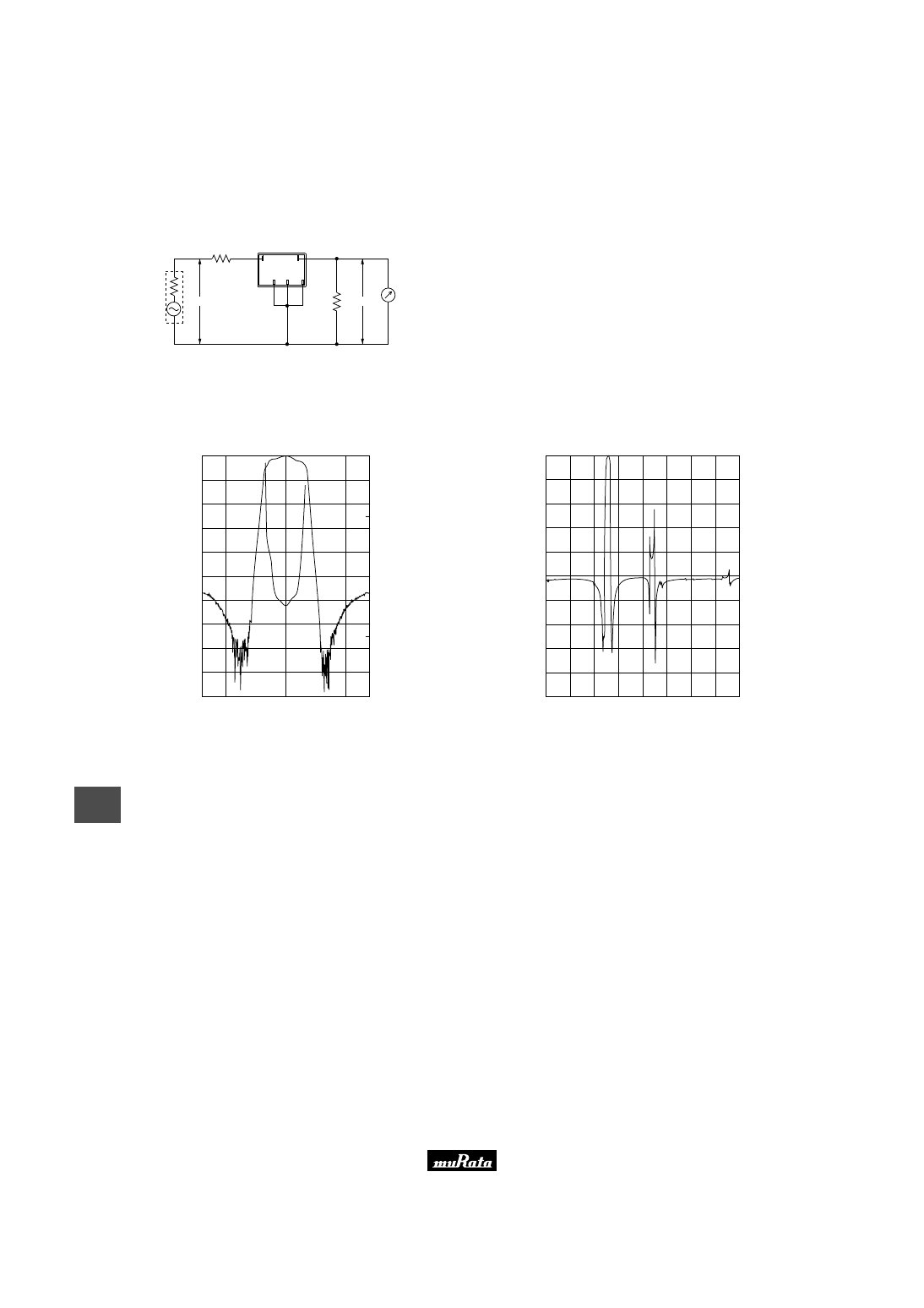
38
13
!
Note
• Please read rating and
!
CAUTION (for storage and operating, rating, soldering and mounting, handling) in this catalog to prevent smoking and/or burning, etc.
• This catalog has only typical specifications because there is no space for detailed specifications. Therefore, please approve our product specification or transact the approval sheet for product specification before ordering.
■ Test Circuit
(1)
(2)
(3)
(4)
(5)
R1
R2
E2
E1
Rg
S.S.G.
0dBm
RF Voltmeter
Connection
(1) : Input
(3)(4)(5) : Ground
(2) : Output
Rg+R1=R2=Input/Output Impedance
■ Frequency Characteristics
CFWLB455KEFA-B0
100
40
30
20
10
0
A
tt
e
n
u
a
ti
o
n
(
d
B
)
0
50
100
200
G
.D
.T
.
(
µ
s
e
c
.)
430
455
480
Frequency (kHz)
90
80
70
60
50
150
CFWLB455KEFA-B0
100
40
30
20
10
0
A
tt
e
n
u
a
ti
o
n
(
d
B
)
200
Frequency (kHz)
90
80
70
60
50
300
400
500
600
700
800
900
1000
Please read rating and
!
CAUTION (for storage and operating, rating, soldering and mounting, handling) in this PDF catalog to prevent smoking and/or burning, etc.
This catalog has only typical specifications. Therefore, you are requested to approve our product specification or to transact the approval sheet for product specificaion before ordering.
!
Note
P05E11.pdf 02.9.2
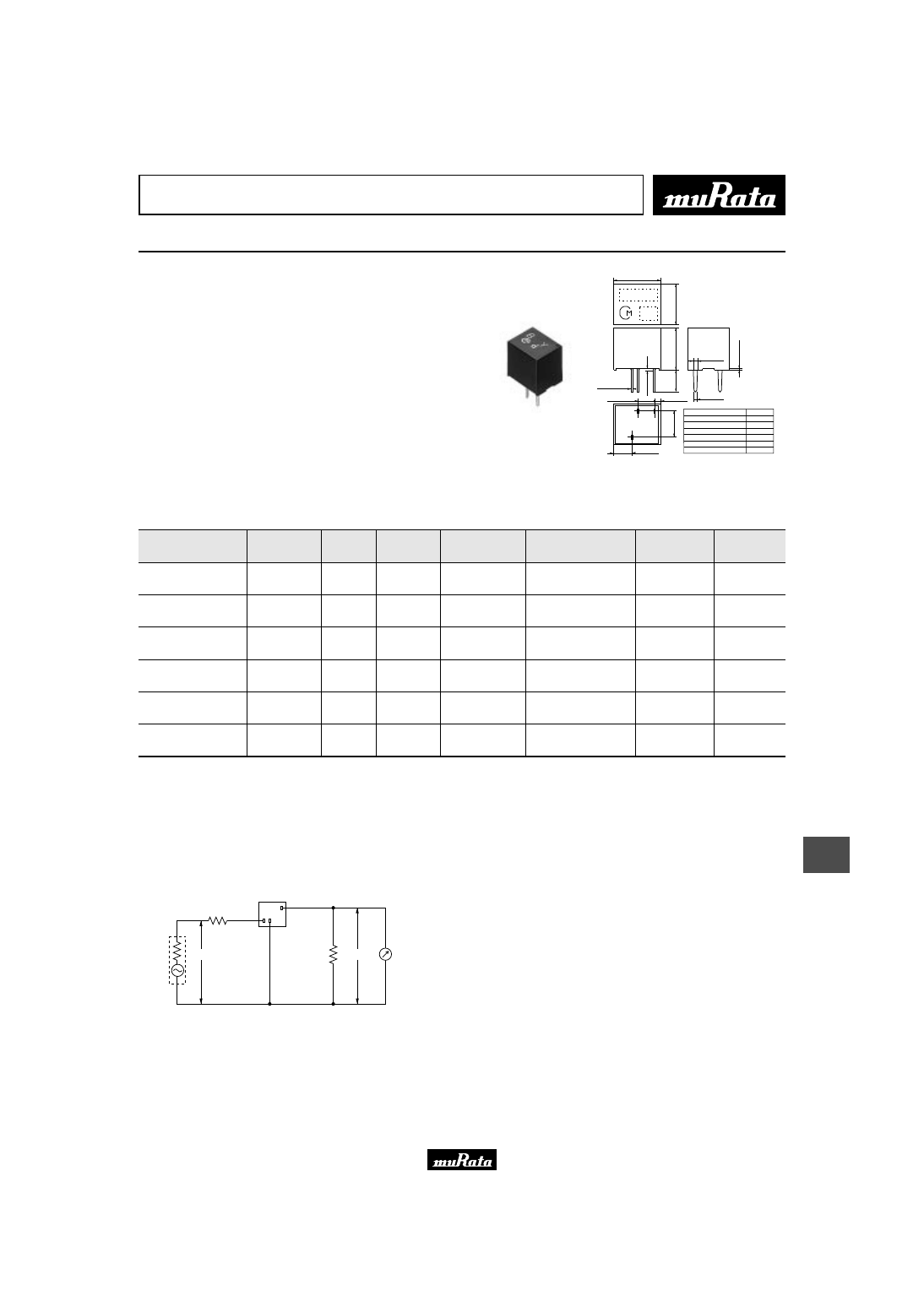
39
14
!
Note
• Please read rating and
!
CAUTION (for storage and operating, rating, soldering and mounting, handling) in this catalog to prevent smoking and/or burning, etc.
• This catalog has only typical specifications because there is no space for detailed specifications. Therefore, please approve our product specification or transact the approval sheet for product specification before ordering.
Ceramic Filters (CERAFILr)/Ceramic Discriminators for Communications Equipment
CERAFIL
r
Plastic Case Group Delay Flat Type CFULA_Y Series
CFULA_Y series are high selectivity ceramic filters,
which consist of 4 ceramic elements connected in a
ladder form.
Most suitable for digital communications and cellular
phones because of their improved GDT characteristics.
■ Features
1. High selectivity.
2. A variety of bandwidth available.
3. Excellent GDT characteristics are available within
pass bandwidth.
4. Easily mounted on a printed circuit board
5. Operating temperature range : -20 to +80 (degree C)
Storage temperature range : -40 to +85 (degree C)
3
.0
±
0
.3
7
.0
±
0
.3
4
.2
±
0
.3
7
.3
±
0
.3
0.8
±
0.1
0.6
±
0.1
1.2
±
0.5
8.0
±
0.3
3.3
±
0.5
2.7
±
0.3
(1)
(2)
(3)
0
.3
±
0
.1
1
.5
m
a
x
.
0.15
±
0.05
Connection
(1) : Input
(2) : Ground
(3) : Output
(in mm)
Type
CFULA455KB4Y-B0
CFULA455KC4Y-B0
CFULA455KD1Y-B0
CFULA455KE1Y-B0
CFULA455KF1Y-B0
CFULA455KG1Y-B0
Marking
BY
CY
DY
EY
FY
GY
MARKING
EIAJ
CODE
Part Number
Center
Frequency (fo)
(kHz)
6dB
Bandwidth
(kHz)
Stop
Bandwidth
(kHz)
Stop Band
Attenuation
(dB)
Insertion
Loss
(dB)
GDT Deviation
(
µ
s)
Input/Output
Impedance
(ohm)
CFULA455KB4Y-B0
455.0
±
1.5kHz
fn
±
15.0
min.
fn
±
35.0 max.
[within 40dB]
25 min.
[within fn
±
100kHz]
5.0 max.
[at minimum loss point]
15.0 max.
[within fn
±
10kHz]
1500
CFULA455KC4Y-B0
455.0
±
1.5kHz
fn
±
12.5
min.
fn
±
30.0 max.
[within 40dB]
25 min.
[within fn
±
100kHz]
6.0 max.
[at minimum loss point]
15.0 max.
[within fn
±
8kHz]
1500
CFULA455KD1Y-B0
455.0
±
1.0kHz
fn
±
10.0
min.
fn
±
25.0 max.
[within 40dB]
23 min.
[within fn
±
100kHz]
7.0 max.
[at minimum loss point]
20.0 max.
[within fn
±
7kHz]
1500
CFULA455KE1Y-B0
455.0
±
1.0kHz
fn
±
7.5
min.
fn
±
20.0 max.
[within 40dB]
23 min.
[within fn
±
100kHz]
8.0 max.
[at minimum loss point]
20.0 max.
[within fn
±
5kHz]
1500
CFULA455KF1Y-B0
455.0
±
1.0kHz
fn
±
6.0
min.
fn
±
17.5 max.
[within 40dB]
23 min.
[within fn
±
100kHz]
9.0 max.
[at minimum loss point]
20.0 max.
[within fn
±
4kHz]
2000
CFULA455KG1Y-B0
455.0
±
1.0kHz
fn
±
4.5
min.
fn
±
15.0 max.
[within 40dB]
23 min.
[within fn
±
100kHz]
10.0 max.
[at minimum loss point]
20.0 max.
[within fn
±
3kHz]
2000
For safety purposes, connect the output of filters to the IF amplifier through a D.C. blocking capacitor. Avoid applying a direct current to the output of ceramic filters.
(fn) means nominal center frequency 455kHz.
The order quantity should be an integral multiple of the "Minimum Quantity" shown in package page in this catalog.
■ Test Circuit
E1
R1
Rg
S.S.G.
0dBm
R2
E2
RF Voltmeter
Connection
(1) : Input
(2) : Ground
(3) : Output
(1) (2)
(3)
Rg+R1=R2=Input/Output Impedance
Please read rating and
!
CAUTION (for storage and operating, rating, soldering and mounting, handling) in this PDF catalog to prevent smoking and/or burning, etc.
This catalog has only typical specifications. Therefore, you are requested to approve our product specification or to transact the approval sheet for product specificaion before ordering.
!
Note
P05E11.pdf 02.9.2
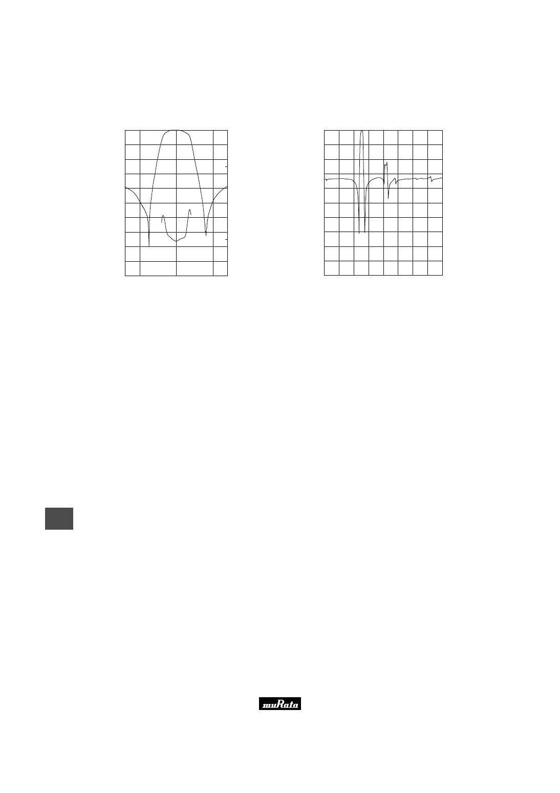
40
14
!
Note
• Please read rating and
!
CAUTION (for storage and operating, rating, soldering and mounting, handling) in this catalog to prevent smoking and/or burning, etc.
• This catalog has only typical specifications because there is no space for detailed specifications. Therefore, please approve our product specification or transact the approval sheet for product specification before ordering.
■ Frequency Characteristics
CFULA455KE1Y-B0
A
tt
e
n
u
a
ti
o
n
(
d
B
)
Frequency (kHz)
G
ro
u
p
D
e
la
y
T
im
e
(
µ
s
e
c
)
430
455
480
10
20
30
40
50
60
70
80
90
100
200
150
100
50
0
0
CFULA455KE1Y-B0
200
300
400
500
600
700
800
900
1000
10
20
30
40
50
60
70
80
90
A
tt
e
n
u
a
ti
o
n
(
d
B
)
Frequency (kHz)
0
100
Please read rating and
!
CAUTION (for storage and operating, rating, soldering and mounting, handling) in this PDF catalog to prevent smoking and/or burning, etc.
This catalog has only typical specifications. Therefore, you are requested to approve our product specification or to transact the approval sheet for product specificaion before ordering.
!
Note
P05E11.pdf 02.9.2
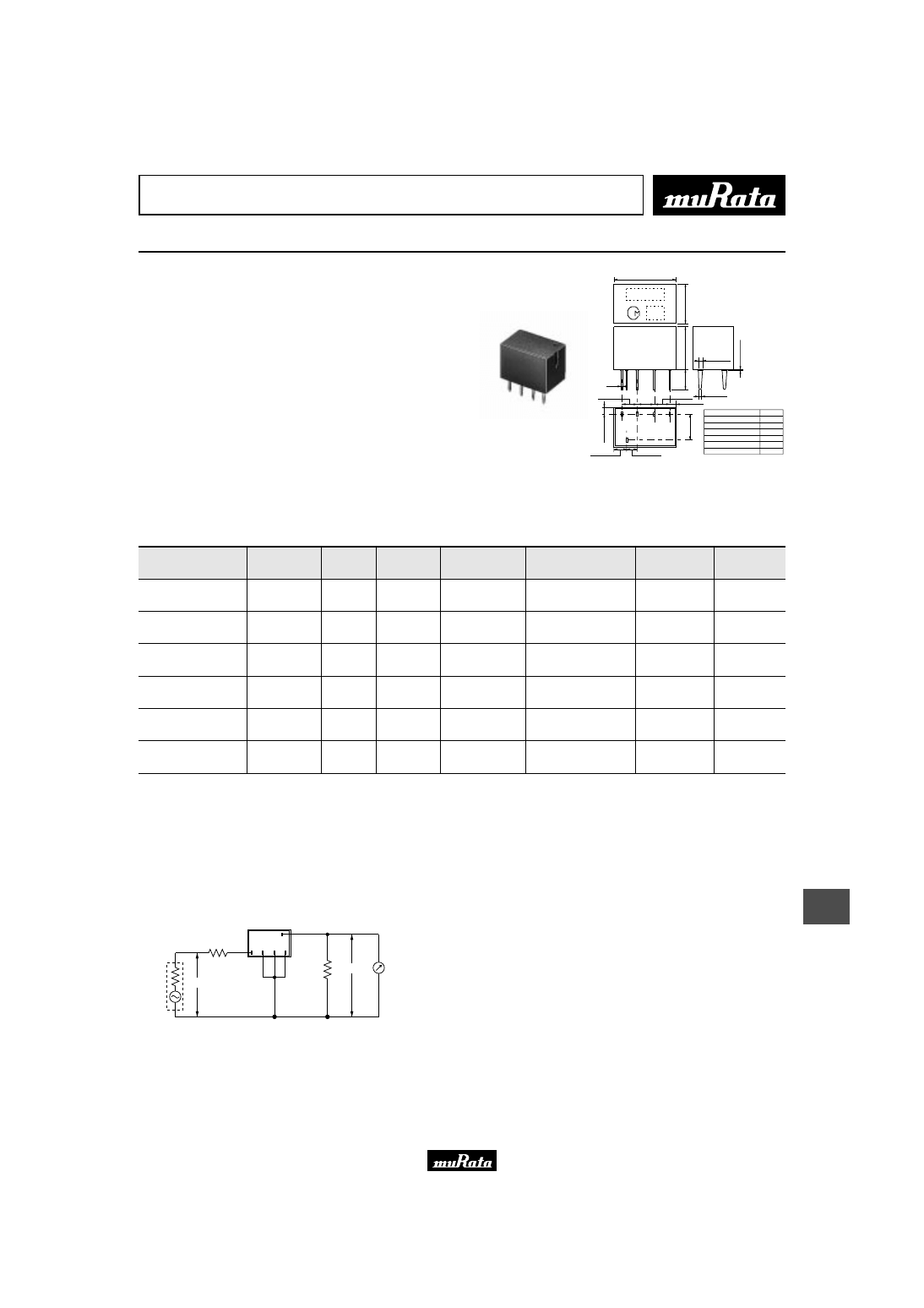
41
15
!
Note
• Please read rating and
!
CAUTION (for storage and operating, rating, soldering and mounting, handling) in this catalog to prevent smoking and/or burning, etc.
• This catalog has only typical specifications because there is no space for detailed specifications. Therefore, please approve our product specification or transact the approval sheet for product specification before ordering.
Ceramic Filters (CERAFILr)/Ceramic Discriminators for Communications Equipment
CERAFIL
r
Plastic Case Group Delay Flat Type CFWLA_Y Series
CFWLA_Y series are high selectivity ceramic filters,
which consist of 6 ceramic elements connected in a
ladder form.
Most suitable for digital communications and mobile
telephones because of their improved GDT
characteristics.
■ Features
1. High selectivity.
2. A variety of bandwidths are available.
3. Excellent GDT characteristics are available within
pass bandwidth.
4. Easily mounted on a printed circuit board
5. Operating temperature range : -20 to +80 (degree C)
Storage temperature range : -40 to +85 (degree C)
4
.3
±
0
.3
0.15
1
.5
m
a
x
.
2.3
±
0.3
2.0
±
0.3
2.9
±
0.3
11.0
±
0.5
1.2
±
0.5
(1)
(2)
(4) (3)
(5)
1
.3
5
±
0
.5
7
.0
±
0
.5
3.
5
±
0.
5
0.6
±
0.1
0.8
±
0.1
7
.5
±
0
.5
2.6
±
0.3
2.9
2.9—
—0.3
0.3
2.9
±
0.3
Type
CFWLA455KB4Y-B0
CFWLA455KC4Y-B0
CFWLA455KD1Y-B0
CFWLA455KE1Y-B0
CFWLA455KF1Y-B0
CFWLA455KG1Y-B0
Marking
BY
CY
DY
EY
FY
GY
Connection
(1) : Input
(2)
(3) : Ground
(4)
(5) : Output
(in mm)
}
MARKING
EIAJ
CODE
Part Number
Center
Frequency (fo)
(kHz)
6dB
Bandwidth
(kHz)
Stop
Bandwidth
(kHz)
Stop Band
Attenuation
(dB)
Insertion
Loss
(dB)
GDT Deviation
(
µ
s)
Input/Output
Impedance
(ohm)
CFWLA455KB4Y-B0
455.0
±
1.5kHz
fn
±
15.0
min.
fn
±
35.0 max.
[within 50dB]
40 min.
[within fn
±
100kHz]
6.0 max.
[at minimum loss point]
30.0 max.
[within fn
±
10kHz]
1500
CFWLA455KC4Y-B0
455.0
±
1.5kHz
fn
±
12.5
min.
fn
±
30.0 max.
[within 50dB]
40 min.
[within fn
±
100kHz]
7.0 max.
[at minimum loss point]
30.0 max.
[within fn
±
8kHz]
1500
CFWLA455KD1Y-B0
455.0
±
1.0kHz
fn
±
10.0
min.
fn
±
25.0 max.
[within 50dB]
40 min.
[within fn
±
100kHz]
8.0 max.
[at minimum loss point]
30.0 max.
[within fn
±
7kHz]
1500
CFWLA455KE1Y-B0
455.0
±
1.0kHz
fn
±
7.5
min.
fn
±
20.0 max.
[within 50dB]
40 min.
[within fn
±
100kHz]
9.0 max.
[at minimum loss point]
30.0 max.
[within fn
±
5kHz]
1500
CFWLA455KF1Y-B0
455.0
±
1.0kHz
fn
±
6.0
min.
fn
±
17.5 max.
[within 50dB]
40 min.
[within fn
±
100kHz]
10.0 max.
[at minimum loss point]
40.0 max.
[within fn
±
4kHz]
2000
CFWLA455KG1Y-B0
455.0
±
1.0kHz
fn
±
4.5
min.
fn
±
15.0 max.
[within 50dB]
40 min.
[within fn
±
100kHz]
11.0 max.
[at minimum loss point]
40.0 max.
[within fn
±
3kHz]
2000
For safety purposes, connect the output of filters to the IF amplifier through a D.C. blocking capacitor. Avoid applying a direct current to the output of ceramic filters.
(fn) means nominal center frequency 455kHz.
The order quantity should be an integral multiple of the "Minimum Quantity" shown in package page in this catalog.
■ Test Circuit
E1
R1
R2
E2
RF Voltmeter
Connection
(1) : Input
(5) : Output
(2)(3)(4) : Ground
Rg
S.S.G.
0dBm
(1) (2) (3) (4)
(5)
Rg+R1=R2=Input/Output Impedance
Please read rating and
!
CAUTION (for storage and operating, rating, soldering and mounting, handling) in this PDF catalog to prevent smoking and/or burning, etc.
This catalog has only typical specifications. Therefore, you are requested to approve our product specification or to transact the approval sheet for product specificaion before ordering.
!
Note
P05E11.pdf 02.9.2
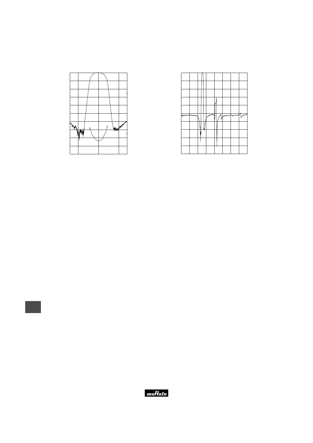
42
15
!
Note
• Please read rating and
!
CAUTION (for storage and operating, rating, soldering and mounting, handling) in this catalog to prevent smoking and/or burning, etc.
• This catalog has only typical specifications because there is no space for detailed specifications. Therefore, please approve our product specification or transact the approval sheet for product specification before ordering.
■ Frequency Characteristics
CFWLA455KE1Y-B0
A
tt
e
n
u
a
ti
o
n
(
d
B
)
430
455
480
Frequency (kHz)
10
20
30
40
50
60
70
80
90
100
400
300
200
100
0
G
ro
u
p
D
e
la
y
T
im
e
(
µ
s
e
c
)
0
CFWLA455KE1Y-B0
200
300
400
500
600
700
800
900
1000
10
20
30
40
50
60
70
80
90
A
tt
e
n
u
a
ti
o
n
(
d
B
)
Frequency (kHz)
0
100
Please read rating and
!
CAUTION (for storage and operating, rating, soldering and mounting, handling) in this PDF catalog to prevent smoking and/or burning, etc.
This catalog has only typical specifications. Therefore, you are requested to approve our product specification or to transact the approval sheet for product specificaion before ordering.
!
Note
P05E11.pdf 02.9.2
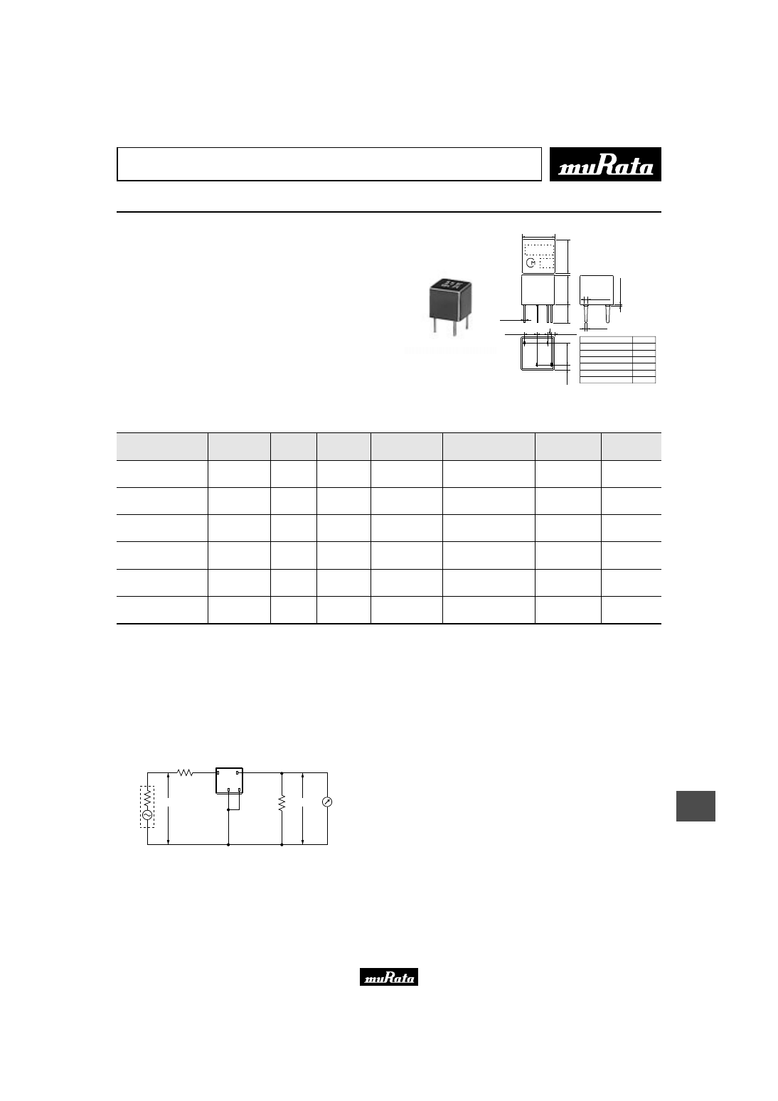
43
16
!
Note
• Please read rating and
!
CAUTION (for storage and operating, rating, soldering and mounting, handling) in this catalog to prevent smoking and/or burning, etc.
• This catalog has only typical specifications because there is no space for detailed specifications. Therefore, please approve our product specification or transact the approval sheet for product specification before ordering.
Ceramic Filters (CERAFILr)/Ceramic Discriminators for Communications Equipment
CERAFIL
r
Plastic Case Group Delay Flat Type Miniaturized Type CFULB_Y Series
Ceramic filter CFULB_Y series are miniature and high
performance filters. These filters, with only 6.3mm
high, are 65% the volume of conventional types
(CFULA455K_Y series).
Well suited for miniaturizing the communications
equipment, especially for a cellular phone.
■ Features
1. Miniature, flat GDT characteristics.
2. Suitable for a cellular phone.
3. A variety of band width are available.
4. Operating temperature range : -20 to +80 (degree C)
Storage temperature range : -40 to +85 (degree C)
4
.3
±
0
.3
1
.0
m
a
x
.
1.8
±
0.3
2.4
±
0.3
6.5
±
0.3
0.8
±
0.3
1.
0
±
0.
3
6
.3
±
0
.3
6
.5
±
0
.3
0.5
±
0.1
0.7
±
0.1
3
.5
±
0
.3
0.7
±
0.3
(1)
(2)
(3)
(4)
0.15
±
0.05
Connection
(1) : Input
(2) : Output
(3)
: Ground
(4)
(in mm)
Type
CFULB455KB4Y-B0
CFULB455KC4Y-B0
CFULB455KD1Y-B0
CFULB455KE1Y-B0
CFULB455KF1Y-B0
CFULB455KG1Y-B0
Marking
BY
CY
DY
EY
FY
GY
}
MARKING
EIAJ
CODE
Part Number
Center
Frequency (fo)
(kHz)
6dB
Bandwidth
(kHz)
Stop
Bandwidth
(kHz)
Stop Band
Attenuation
(dB)
Insertion
Loss
(dB)
GDT Deviation
(
µ
s)
Input/Output
Impedance
(ohm)
CFULB455KB4Y-B0
455.0
±
1.5kHz
fn
±
15.0
min.
fn
±
35.0 max.
[within 40dB]
25 min.
[within fn
±
100kHz]
5.0 max.
[at minimum loss point]
15.0 max.
[within fn
±
10kHz]
1500
CFULB455KC4Y-B0
455.0
±
1.5kHz
fn
±
12.5
min.
fn
±
30.0 max.
[within 40dB]
25 min.
[within fn
±
100kHz]
6.0 max.
[at minimum loss point]
15.0 max.
[within fn
±
8kHz]
1500
CFULB455KD1Y-B0
455.0
±
1.0kHz
fn
±
10.0
min.
fn
±
25.0 max.
[within 40dB]
23 min.
[within fn
±
100kHz]
7.0 max.
[at minimum loss point]
20.0 max.
[within fn
±
7kHz]
1500
CFULB455KE1Y-B0
455.0
±
1.0kHz
fn
±
7.5
min.
fn
±
20.0 max.
[within 40dB]
23 min.
[within fn
±
100kHz]
8.0 max.
[at minimum loss point]
20.0 max.
[within fn
±
5kHz]
1500
CFULB455KF1Y-B0
455.0
±
1.0kHz
fn
±
6.0
min.
fn
±
17.5 max.
[within 40dB]
23 min.
[within fn
±
100kHz]
9.0 max.
[at minimum loss point]
20.0 max.
[within fn
±
4kHz]
2000
CFULB455KG1Y-B0
455.0
±
1.0kHz
fn
±
4.5
min.
fn
±
15.0 max.
[within 40dB]
23 min.
[within fn
±
100kHz]
10.0 max.
[at minimum loss point]
20.0 max.
[within fn
±
3kHz]
2000
For safety purposes, connect the output of filters to the IF amplifier through a D.C. blocking capacitor. Avoid applying a direct current to the output of ceramic filters.
(fn) means nominal center frequency 455kHz.
The order quantity should be an integral multiple of the "Minimum Quantity" shown in package page in this catalog.
CFULB455K_Y series filters are 4-element ceramic filters and miniature versions of CFULA455K_Y series.
■ Test Circuit
E1
R1
Rg
S.S.G.
0dBm
R2
E2
RF Voltmeter
Connection
(1) : Input
(2) : Output
(3)(4) :Ground
(1)
(2)
(3)
(4)
Rg+R1=R2=Input/Output Impedance
Please read rating and
!
CAUTION (for storage and operating, rating, soldering and mounting, handling) in this PDF catalog to prevent smoking and/or burning, etc.
This catalog has only typical specifications. Therefore, you are requested to approve our product specification or to transact the approval sheet for product specificaion before ordering.
!
Note
P05E11.pdf 02.9.2
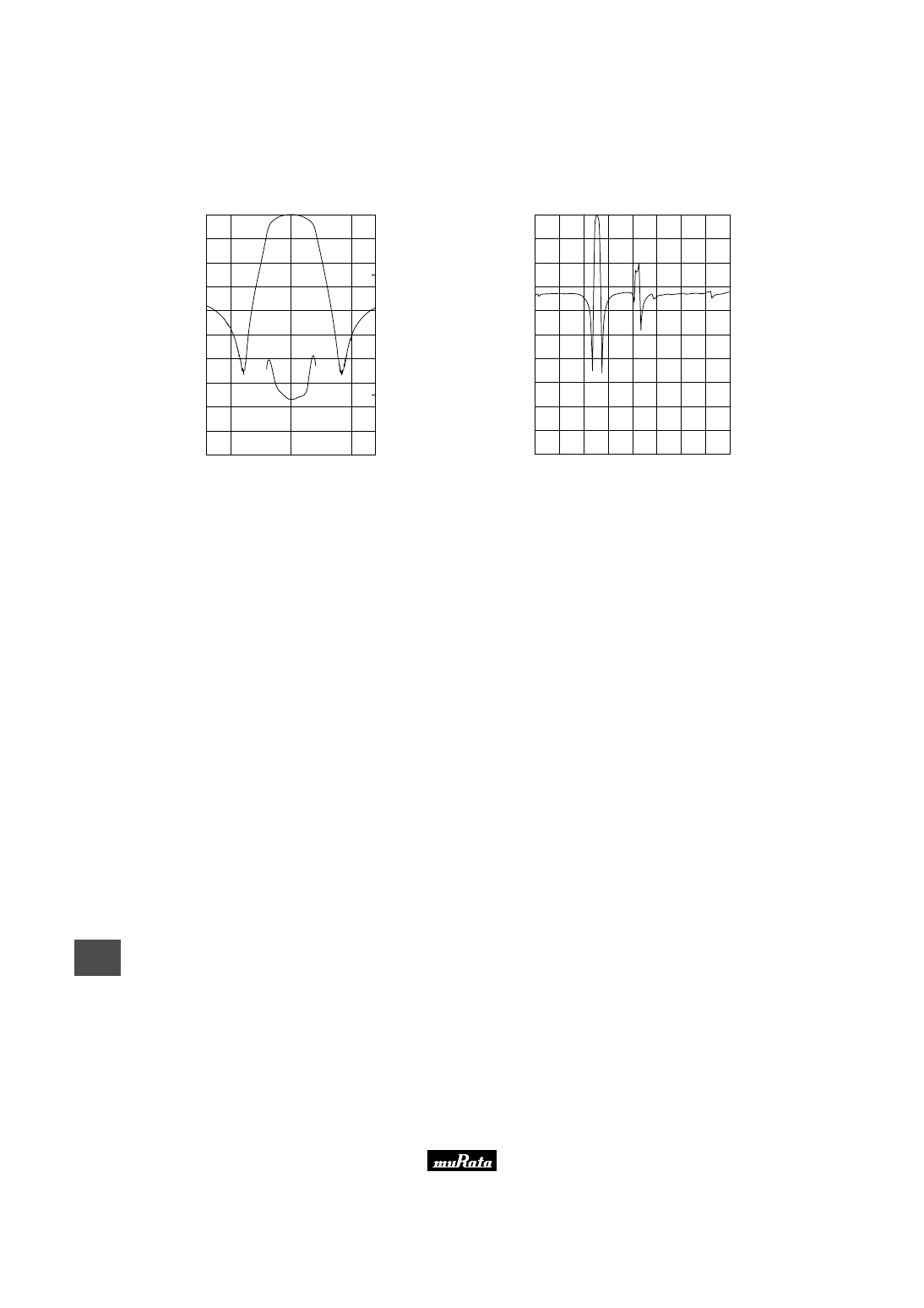
44
16
!
Note
• Please read rating and
!
CAUTION (for storage and operating, rating, soldering and mounting, handling) in this catalog to prevent smoking and/or burning, etc.
• This catalog has only typical specifications because there is no space for detailed specifications. Therefore, please approve our product specification or transact the approval sheet for product specification before ordering.
■ Frequency Characteristics
CFULB455KE1Y-B0
A
tt
e
n
u
a
ti
o
n
(
d
B
)
Frequency (kHz)
G
ro
u
p
D
e
la
y
T
im
e
(
µ
s
e
c
)
430
455
480
10
20
30
40
50
60
70
80
90
100
200
150
100
50
0
0
CFULB455KE1Y-B0
200
300
400
500
600
700
800
900
1000
10
20
30
40
50
60
70
80
90
A
tt
e
n
u
a
ti
o
n
(
d
B
)
Frequency (kHz)
0
100
Please read rating and
!
CAUTION (for storage and operating, rating, soldering and mounting, handling) in this PDF catalog to prevent smoking and/or burning, etc.
This catalog has only typical specifications. Therefore, you are requested to approve our product specification or to transact the approval sheet for product specificaion before ordering.
!
Note
P05E11.pdf 02.9.2
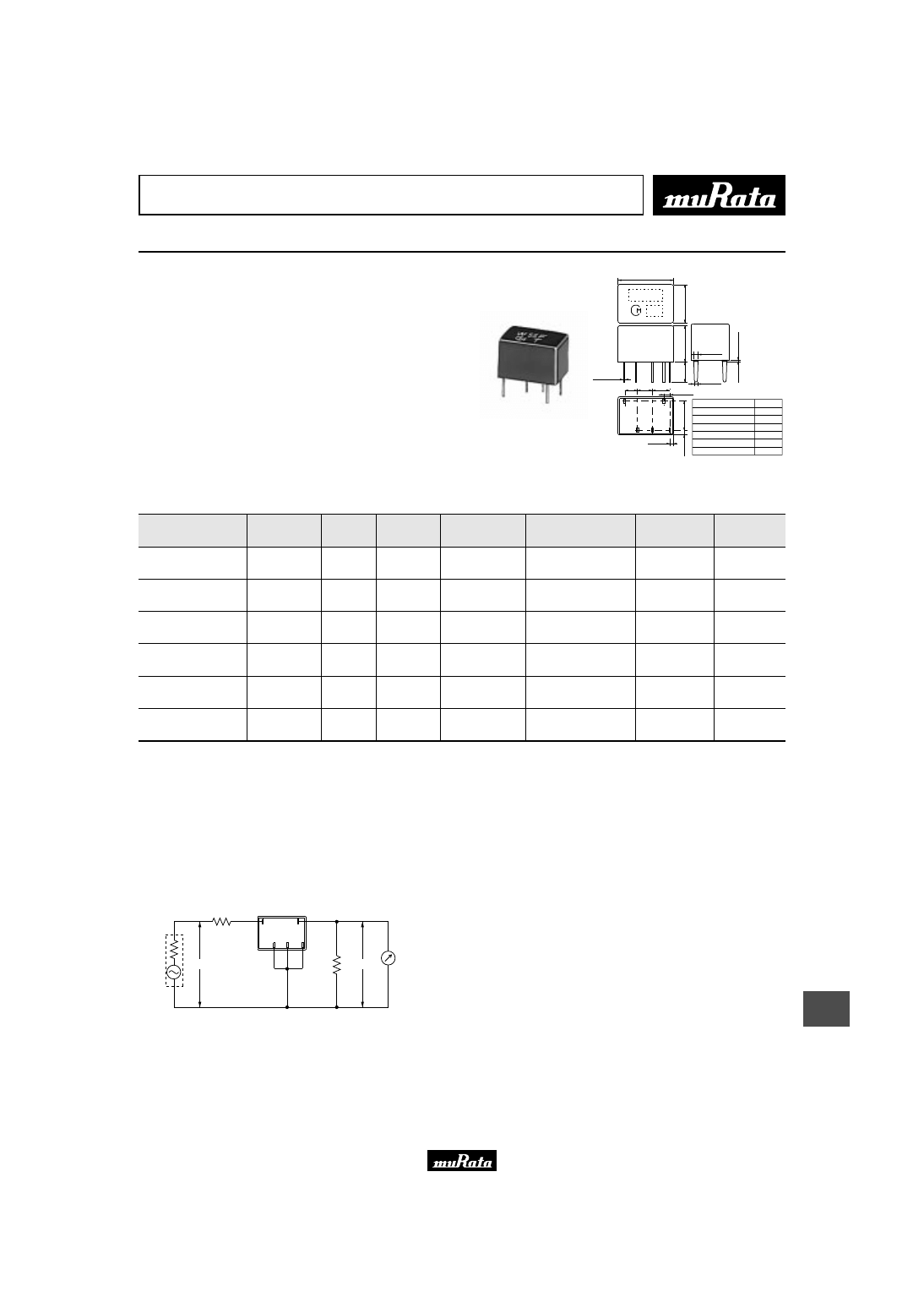
45
17
!
Note
• Please read rating and
!
CAUTION (for storage and operating, rating, soldering and mounting, handling) in this catalog to prevent smoking and/or burning, etc.
• This catalog has only typical specifications because there is no space for detailed specifications. Therefore, please approve our product specification or transact the approval sheet for product specification before ordering.
Ceramic Filters (CERAFILr)/Ceramic Discriminators for Communications Equipment
CERAFIL
r
Plastic Case Group Delay Flat Type CFWLB_Y Series
Ceramic filter CFWLB_Y series are miniature and
high-performance filters. These filters, with only
6.3mm high, are 67% the volume of conventional types
(CFWLA455K_Y series).
Well suited for miniaturizing the communications
equipment, especially for a cellular phone.
■ Features
1. Miniature, flat GDT characteristics.
2. Suitable for a cellular phone.
3. A variety of band width are available.
4. Operating temperature range : -20 to +80 (degree C)
Storage temperature range : -40 to +85 (degree C)
4
.3
±
0
.3
1
.0
m
a
x
.
2.7
±
0.3
2.5
±
0.3
9.5
±
0.3
0.7
±
0.3
1
.0
±
0
.3
6
.3
±
0
.3
6
.5
±
0
.3
0.5
±
0.1
0.7
±
0.1
3
.5
±
0
.3
0.9
±
0.3
0.15
±
0.05
(1)
(3)
(4)
(2)
(5)
2.8
±
0.3
Type
CFWLB455KB4Y-B0
CFWLB455KC4Y-B0
CFWLB455KD1Y-B0
CFWLB455KE1Y-B0
CFWLB455KF1Y-B0
CFWLB455KG1Y-B0
Marking
BY
CY
DY
EY
FY
GY
Connection
(1) : Input
(2) : Output
(3)
(4) : Ground
(5)
(in mm)
}
MARKING
EIAJ
CODE
Part Number
Center
Frequency (fo)
(kHz)
6dB
Bandwidth
(kHz)
Stop
Bandwidth
(kHz)
Stop Band
Attenuation
(dB)
Insertion
Loss
(dB)
GDT Deviation
(
µ
s)
Input/Output
Impedance
(ohm)
CFWLB455KB4Y-B0
455.0
±
1.5kHz
fn
±
15.0
min.
fn
±
30.0 max.
[within 50dB]
40 min.
[within fn
±
100kHz]
6.0 max.
[at minimum loss point]
30.0 max.
[within fn
±
10kHz]
1500
CFWLB455KC4Y-B0
455.0
±
1.5kHz
fn
±
12.5
min.
fn
±
27.5 max.
[within 50dB]
40 min.
[within fn
±
100kHz]
7.0 max.
[at minimum loss point]
30.0 max.
[within fn
±
8kHz]
1500
CFWLB455KD1Y-B0
455.0
±
1.0kHz
fn
±
10.0
min.
fn
±
25.0 max.
[within 50dB]
40 min.
[within fn
±
100kHz]
8.0 max.
[at minimum loss point]
30.0 max.
[within fn
±
7kHz]
1500
CFWLB455KE1Y-B0
455.0
±
1.0kHz
fn
±
7.5
min.
fn
±
20.0 max.
[within 50dB]
40 min.
[within fn
±
100kHz]
9.0 max.
[at minimum loss point]
30.0 max.
[within fn
±
5kHz]
1500
CFWLB455KF1Y-B0
455.0
±
1.0kHz
fn
±
6.0
min.
fn
±
17.5 max.
[within 50dB]
40 min.
[within fn
±
100kHz]
10.0 max.
[at minimum loss point]
40.0 max.
[within fn
±
4kHz]
2000
CFWLB455KG1Y-B0
455.0
±
1.0kHz
fn
±
4.5
min.
fn
±
15.0 max.
[within 50dB]
40 min.
[within fn
±
100kHz]
11.0 max.
[at minimum loss point]
40.0 max.
[within fn
±
3kHz]
2000
For safety purposes, connect the output of filters to the IF amplifier through a D.C. blocking capacitor. Avoid applying a direct current to the output of ceramic filters.
(fn) means nominal center frequency 455kHz.
The order quantity should be an integral multiple of the "Minimum Quantity" shown in package page in this catalog.
CFWLB455K_Y series filters are 4-element ceramic filters and miniature versions of CFWLA455K_Y series.
■ Test Circuit
(1)
(2)
(3)
(4)
(5)
R1
R2
E2
E1
Rg
S.S.G.
0dBm
RF Voltmeter
Connection
(1) : Input
(3)(4)(5) : Ground
(2) : Output
Rg+R1=R2=Input/Output Impedance
Please read rating and
!
CAUTION (for storage and operating, rating, soldering and mounting, handling) in this PDF catalog to prevent smoking and/or burning, etc.
This catalog has only typical specifications. Therefore, you are requested to approve our product specification or to transact the approval sheet for product specificaion before ordering.
!
Note
P05E11.pdf 02.9.2
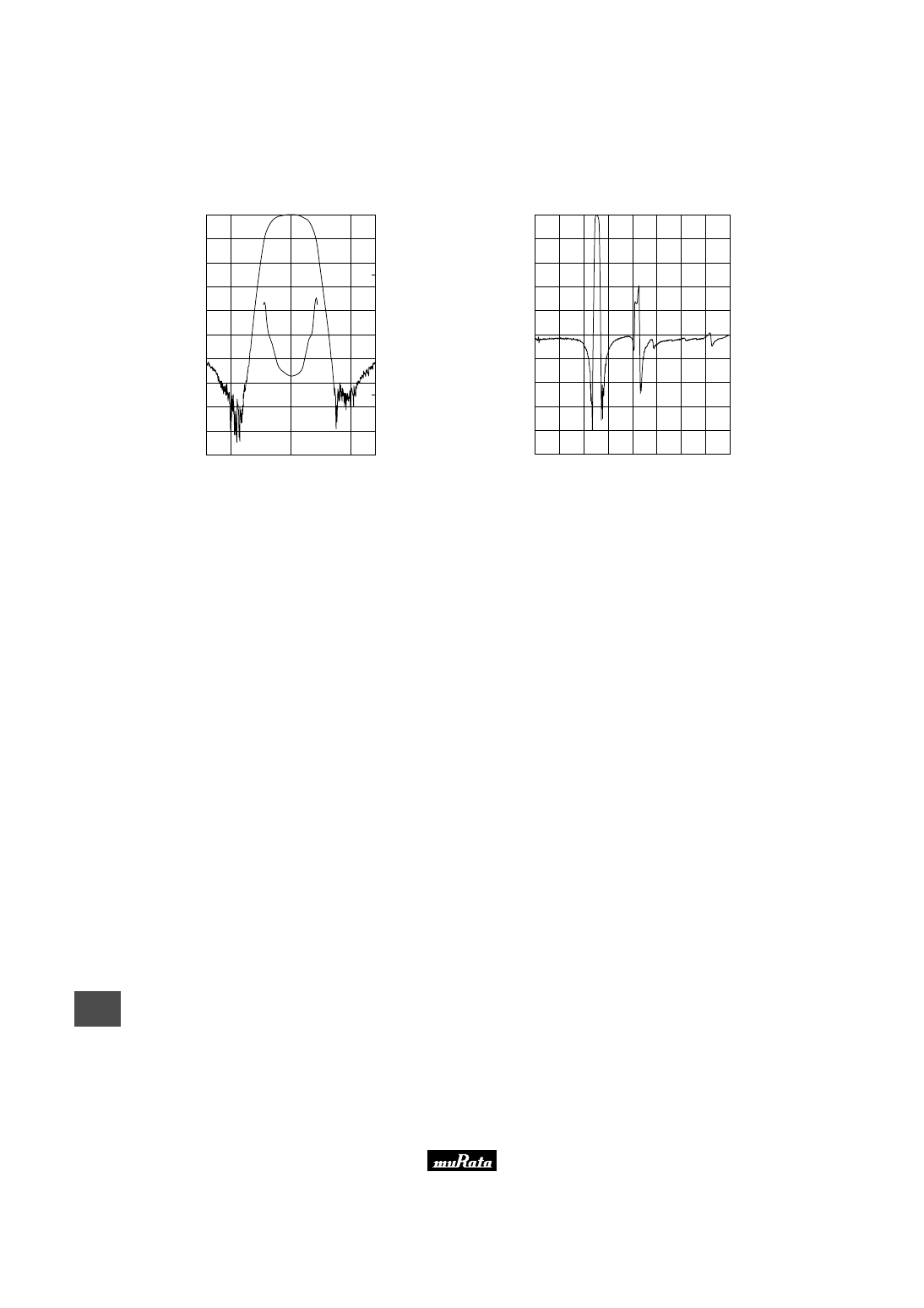
46
17
!
Note
• Please read rating and
!
CAUTION (for storage and operating, rating, soldering and mounting, handling) in this catalog to prevent smoking and/or burning, etc.
• This catalog has only typical specifications because there is no space for detailed specifications. Therefore, please approve our product specification or transact the approval sheet for product specification before ordering.
■ Frequency Characteristics
CFWLB455KE1Y-B0
A
tt
e
n
u
a
ti
o
n
(
d
B
)
430
455
480
Frequency (kHz)
10
20
30
40
50
60
70
80
90
100
200
150
100
50
0
G
ro
u
p
D
e
la
y
T
im
e
(
µ
s
e
c
)
0
CFWLB455KE1Y-B0
200
300
400
500
600
700
800
900
1000
10
20
30
40
50
60
70
80
90
A
tt
e
n
u
a
ti
o
n
(
d
B
)
Frequency (kHz)
0
100
Please read rating and
!
CAUTION (for storage and operating, rating, soldering and mounting, handling) in this PDF catalog to prevent smoking and/or burning, etc.
This catalog has only typical specifications. Therefore, you are requested to approve our product specification or to transact the approval sheet for product specificaion before ordering.
!
Note
P05E11.pdf 02.9.2
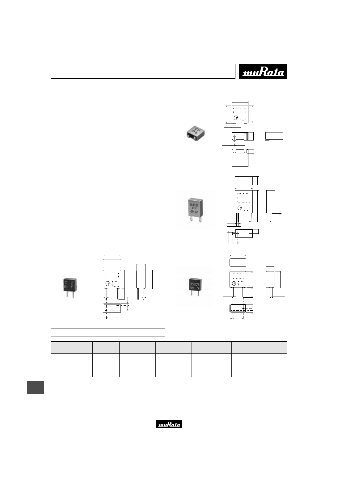
48
18
!
Note
• Please read rating and
!
CAUTION (for storage and operating, rating, soldering and mounting, handling) in this catalog to prevent smoking and/or burning, etc.
• This catalog has only typical specifications because there is no space for detailed specifications. Therefore, please approve our product specification or transact the approval sheet for product specification before ordering.
Ceramic Filters (CERAFILr)/Ceramic Discriminators for Communications Equipment
kHz Type Ceramic Discriminators
Ceramic discriminator consists of wide band
piezoelectric resonator.
It is ideal for mobile communication equipments due to
its small size and light weight.
Standard line include products for wide range of
application, from cordless telecom to cellular
telephone, making non-adjustment and shrinking of the
detection circuit possible.
■ Features
1. Small in size and light weight.
2. Realize no-adjustment in detection circuit.
3. High sensitivity and stability.
4. Wide range of standard products are available for
various ICs.
5. Operating temperature range : -20 to +80 (degree C)
Storage temperature range : -40 to +85 (degree C)
MARKING
EIAJ
CODE
6
.6
±
0
.3
1
.5
±
0
.3
6.0
±
0.2
1.15
±
0.2
1.0
±
0.1
3.7
±
0.2
3
.1
m
a
x
.
6
.2
±
0
.2
(in mm)
CDBCB Series
0
.2
5
±
0
.0
5
5.0
±
0.2
(in mm)
MARKING
EIAJ
CODE
3
.5
±
0
.5
9
.0
±
0
.3
3
.5
±
0
.3
1
.5
m
a
x
.
0
.1
±
0
.0
5
1
.7
5
±
0
.5
0.8
±
0.1
1.1
±
0.1
7.0
±
0.3
CDBLA Series
(in mm)
MARKING
EIAJ
CODE
0
.6
±
0
.2
1
.8
±
0
.2
6
.3
m
a
x
.
4.2
±
0.2
6.0
±
0.2
0.5
±
0.1
0.15
±
0.05
0.9
±
0.2
3.0
±
0.3
6
.0
m
a
x
.
4
.2
±
0
.5
CDBLB_CAX Series
(in mm)
MARKING
EIAJ
CODE
1
.5
±
0
.3
1
.0
±
0
.3
0
.5
±
0
.2
6
.3
m
a
x
.
4.2
±
0.2
6.0
±
0.2
0.5
±
0.1
0.15
±
0.05
0.9
±
0.2
3.0
±
0.3
6
.0
m
a
x
.
4
.2
±
0
.5
CDBLB_CAY Series
Specified by Impedance Characteristics 1
Part Number
Nominal Center
Frequency (fn)
(kHz)
Inclination of
Impedance Curve(1)
Inclination of
Impedance Curve(2)
Capacitance
(C)
IC
IC Maker
Type
CDBLB455KCAX02-B0
455
447.0
±
1.5kHz
(at |Z|=2.05kohm)
463.0
±
1.5kHz
(at |Z|=10.0kohm)
140pF
±
20%
TA8104F
TOSHIBA
PLASTIC
CDBLB455KCAX31-B0
455
447.0
±
1.5kHz
(at |Z|=2.05kohm)
463.0
±
1.5kHz
(at |Z|=10.0kohm)
140pF
±
20%
TA31141
TOSHIBA
PLASTIC
Please read rating and
!
CAUTION (for storage and operating, rating, soldering and mounting, handling) in this PDF catalog to prevent smoking and/or burning, etc.
This catalog has only typical specifications. Therefore, you are requested to approve our product specification or to transact the approval sheet for product specificaion before ordering.
!
Note
P05E11.pdf 02.9.2
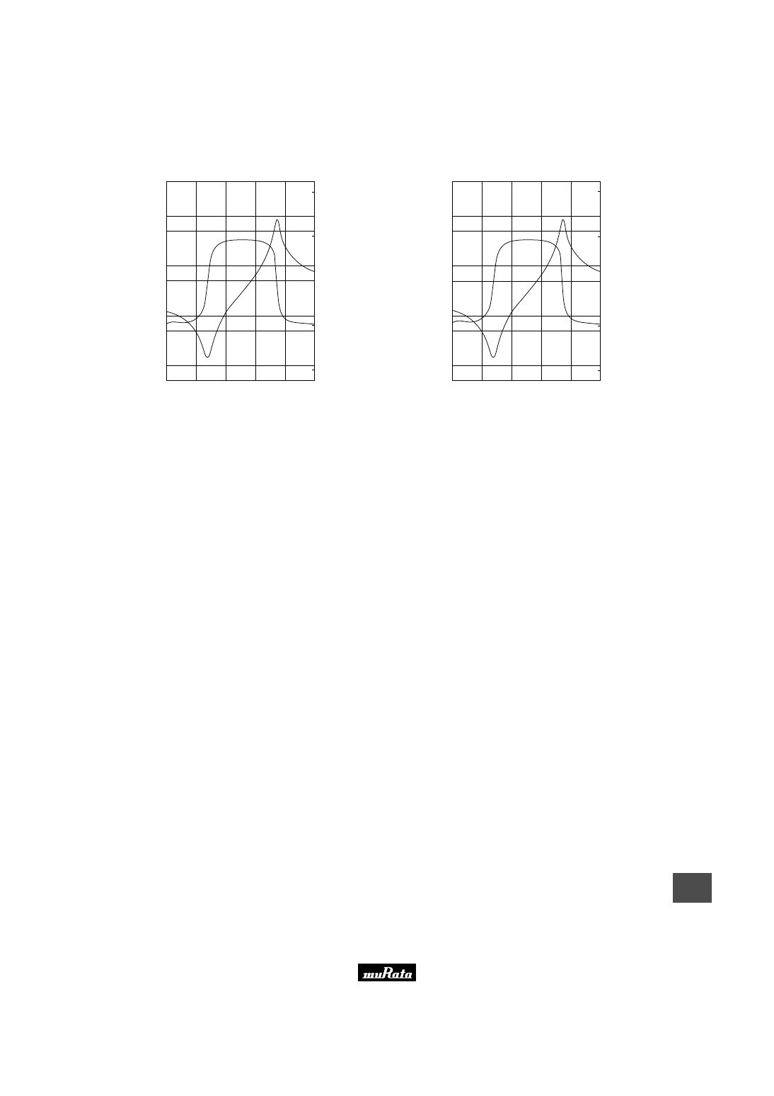
49
18
!
Note
• Please read rating and
!
CAUTION (for storage and operating, rating, soldering and mounting, handling) in this catalog to prevent smoking and/or burning, etc.
• This catalog has only typical specifications because there is no space for detailed specifications. Therefore, please approve our product specification or transact the approval sheet for product specification before ordering.
■ Impedance Curve Specification 1
CDBLB455KCAX02-B0
500K
180
50K
90
10K
5K
0
1K
500
−
90
100
−
180
Im
p
e
d
a
n
c
e
(
Ω
)
P
h
a
s
e
(
d
e
g
)
400
420
440
460
480
Frequency (kHz)
500
100K
50
CDBLB455KCAX31-B0
500K
180
50K
90
10K
5K
0
1K
500
−
90
100
−
180
Im
p
e
d
a
n
c
e
(
Ω
)
P
h
a
s
e
(
d
e
g
)
400
420
440
460
480
Frequency (kHz)
500
100K
50
Please read rating and
!
CAUTION (for storage and operating, rating, soldering and mounting, handling) in this PDF catalog to prevent smoking and/or burning, etc.
This catalog has only typical specifications. Therefore, you are requested to approve our product specification or to transact the approval sheet for product specificaion before ordering.
!
Note
P05E11.pdf 02.9.2
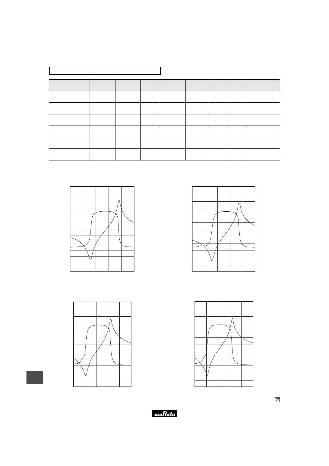
50
18
!
Note
• Please read rating and
!
CAUTION (for storage and operating, rating, soldering and mounting, handling) in this catalog to prevent smoking and/or burning, etc.
• This catalog has only typical specifications because there is no space for detailed specifications. Therefore, please approve our product specification or transact the approval sheet for product specification before ordering.
Specified by Impedance Characteristics 2
Part Number
Nominal Center
Frequency (fn)
(kHz)
Anti-resonant
Frequency (Fa)
Delta F
(Fa-Fr)
Resonant
Resistance (R)
Capacitance
(C)
IC
IC Maker
Type
CDBCB455KCAX33-R0
-
458.0
±
1.5kHz
42
±
4.0kHz
300ohm max.
280pF
±
20%
CXA1474
SONY
SMD
CDBLA455KCAY03-B0
-
455.0
±
1.5kHz
48
±
5.0kHz
70ohm max.
600pF
±
20%
CXA1184
SONY
PLASTIC
CDBLB455KCAY03-B0
-
455.0
±
1.5kHz
46
±
5.0kHz
70ohm max.
550pF
±
20% CXA1184M
SONY
PLASTIC
CDBLB455KCAX15-B0
-
463.5
±
1.0kHz
43
±
2.0kHz
300ohm max.
140pF
±
20% CXA1183M
SONY
PLASTIC
CDBLB455KCAX25-B0
455
465.0
±
1.5kHz
45
±
4.0kHz
300ohm max.
135pF
±
20%
CXA1484
SONY
PLASTIC
CDBLB455KCAX33-B0
455
465.0
±
1.5kHz
45
±
4.0kHz
300ohm max.
135pF
±
20%
CXA1474
SONY
PLASTIC
■ Impedance Curve Specification 2
CDBLA/CDBLB455KCAY03-B0
100K
180
5K
90
1K
500
0
100
50
−
90
−
180
Im
p
e
d
a
n
c
e
(
Ω
)
380
400
420
440
460
Frequency (kHz)
480
10K
10
50K
P
h
a
s
e
(
d
e
g
)
CDBLB455KCAX15-B0
500K
180
50K
90
10K
5K
0
1K
500
−
90
100
−
180
Im
p
e
d
a
n
c
e
(
Ω
)
P
h
a
s
e
(
d
e
g
)
390
410
430
450
470
Frequency (kHz)
490
100K
50
CDBLB455KCAX25-B0
500K
180
50K
90
10K
5K
0
1K
500
−
90
100
−
180
Im
p
e
d
a
n
c
e
(
Ω
)
P
h
a
s
e
(
d
e
g
)
400
420
440
460
480
Frequency (kHz)
500
100K
50
CDBCB455KCAX33-R0
500K
100K
10K
Im
p
e
d
a
n
c
e
(
Ω
)
P
h
a
s
e
(
d
e
g
)
400
420
440
460
480
500
Frequency (kHz)
500
50
180
50K
90
5K
0
−
90
1K
−
180
100
Continued on the following page.
Please read rating and
!
CAUTION (for storage and operating, rating, soldering and mounting, handling) in this PDF catalog to prevent smoking and/or burning, etc.
This catalog has only typical specifications. Therefore, you are requested to approve our product specification or to transact the approval sheet for product specificaion before ordering.
!
Note
P05E11.pdf 02.9.2
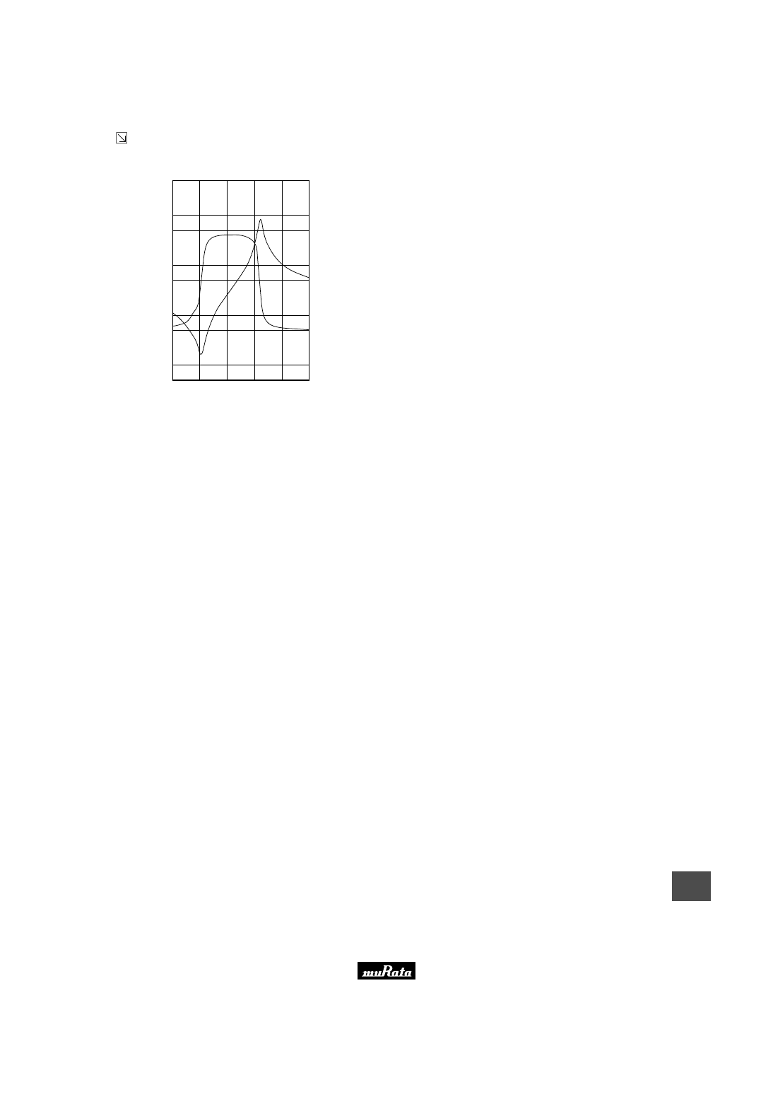
51
18
!
Note
• Please read rating and
!
CAUTION (for storage and operating, rating, soldering and mounting, handling) in this catalog to prevent smoking and/or burning, etc.
• This catalog has only typical specifications because there is no space for detailed specifications. Therefore, please approve our product specification or transact the approval sheet for product specification before ordering.
Continued from the preceding page.
■ Impedance Curve Specification 2
CDBLB455KCAX33-B0
500K
100K
10K
Im
p
e
d
a
n
c
e
(
Ω
)
P
h
a
s
e
(
d
e
g
)
400
420
440
460
480
500
Frequency (kHz)
500
50
180
50K
90
5K
0
−
90
1K
−
180
100
Please read rating and
!
CAUTION (for storage and operating, rating, soldering and mounting, handling) in this PDF catalog to prevent smoking and/or burning, etc.
This catalog has only typical specifications. Therefore, you are requested to approve our product specification or to transact the approval sheet for product specificaion before ordering.
!
Note
P05E11.pdf 02.9.2
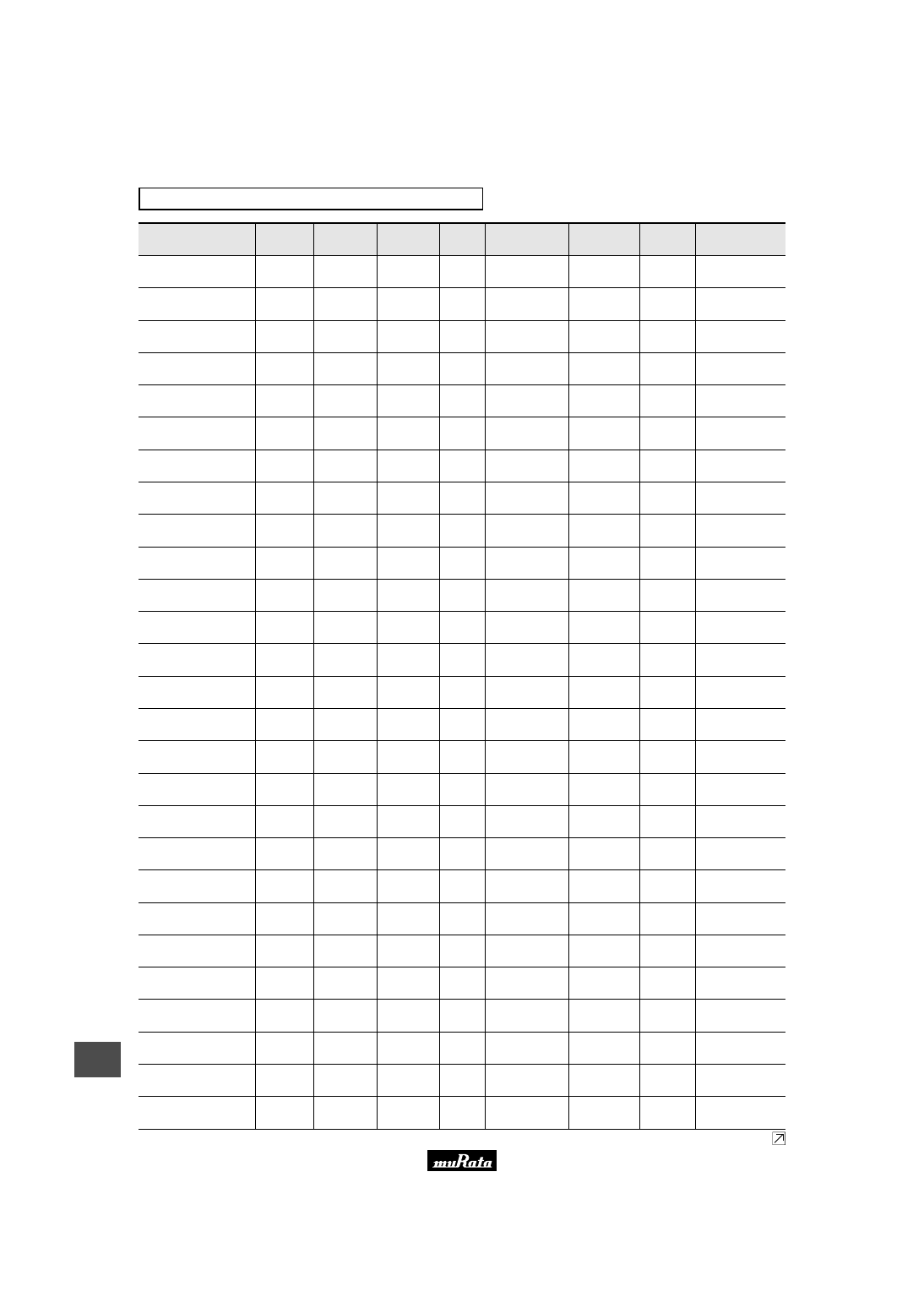
52
18
!
Note
• Please read rating and
!
CAUTION (for storage and operating, rating, soldering and mounting, handling) in this catalog to prevent smoking and/or burning, etc.
• This catalog has only typical specifications because there is no space for detailed specifications. Therefore, please approve our product specification or transact the approval sheet for product specification before ordering.
Specified by Recovered Audio Characteristics
Part Number
Nominal Center
Frequency (fn)
(kHz)
Recovered
Audio 3dB BW
(kHz)
Recovered
Audio Output
(mV)
Distortion
(at fn)
(%)
Distortion
(%)
IC
IC Maker
Type
CDBCB455KCAY07-R0
455
fn
±
4.0 min.
350
±
60
3.0 max.
-
MC3357
MOTOROLA
SMD
CDBCB455KCAY09-R0
455
fn
±
4.0 min.
120
±
40
1.5 max.
-
NE604N
PHILIPS
SMD
CDBCB455KCAY13-R0
455
fn
±
4.0 min.
330
±
50
4.0 max.
-
CXA1003BM
SONY
SMD
CDBCB455KCAY16-R0
455
fn
±
4.0 min.
175
±
40
2.0 max.
-
MC3372
MOTOROLA
SMD
CDBCB455KCAY21-R0
455
fn
±
4.0 min.
55
±
20
2.0 max.
-
TA31132
TOSHIBA
SMD
CDBCB455KCAY24-R0
455
fn
±
4.0 min.
100
±
40
2.0 max.
-
TA31136
TOSHIBA
SMD
CDBCB455KCAY27-R0
455
fn
±
4.0 min.
90
±
30
2.0 max.
-
TK10487
TOKO
SMD
CDBCB455KCAY28-R0
455
fn
±
4.0 min.
40
±
20
3.0 max.
-
TA31142F
TOSHIBA
SMD
CDBCB455KCAY29-R0
455
fn
±
4.0 min.
100
±
30
2.5 max.
-
NE605
PHILIPS
SMD
CDBCB455KCAY32-R0
455
fn
±
4.0 min.
40
±
20
3.0 max.
-
TA31143
TOSHIBA
SMD
CDBCB455KCAY35-R0
455
fn
±
4.0 min.
100
±
40
2.5 max.
-
TK10930
TOKO
SMD
CDBCB455KCAY40-R0
455
fn
±
4.0 min.
40
±
20
3.5 max.
-
TA31145
TOSHIBA
SMD
CDBCB455KCAY49-R0
455
fn
±
4.0 min.
45
±
10
3.0 max.
-
MC3361
MOTOROLA
SMD
CDBCB455KCAY50-R0
455
fn
±
4.0 min.
64
±
6.4
4.0 max.
-
CXA3117N
SONY
SMD
CDBCB455KCLX36-R0
455
fn
±
13.0 min.
90
±
30
2.5 max.
5.0 max.
[within fn
±
6kHz]
NE(SA)606
/NE(SA)616
PHILIPS
SMD
CDBCB455KCLX39-R0
455
fn
±
11.0 min.
130
±
20
2.5 max.
7.0 max.
[within fn
±
8kHz]
NE607
/NE617
PHILIPS
SMD
CDBCB455KCLY13-R0
455
fn
±
13.0 min.
120
±
30
1.5 max.
5.0 max.
[within fn
±
8kHz]
CXA1003BM
SONY
SMD
CDBCB455KCLY21-R0
455
fn
±
11.0 min.
75
±
25
2.5 max.
5.0 max.
[within fn
±
5.5kHz]
TA31132
TOSHIBA
SMD
CDBLA455KCAY07-B0
455
fn
±
4.0 min.
340
±
60
2.5 max.
-
MC3357
MOTOROLA
PLASTIC
CDBLA455KCAY09-B0
455
fn
±
5.0 min.
100 min.
1.5 max.
-
NE604N
PHILIPS
PLASTIC
CDBLA455KCAY13A-B0
455
fn
±
4.0 min.
350
±
50
3.0 max.
-
CXA1003BM
SONY
PLASTIC
CDBLA455KCAY16-B0
455
fn
±
4.0 min.
185
±
40
2.0 max.
-
MC3372
MOTOROLA
PLASTIC
CDBLA455KCAY24-B0
455
fn
±
4.0 min.
100
±
40
2.0 max.
-
TA31136
TOSHIBA
PLASTIC
CDBLA455KCAY28-B0
455
fn
±
4.0 min.
40
±
20
3.0 max.
-
TA31142
TOSHIBA
PLASTIC
CDBLA455KCAY34-B0
455
fn
±
4.0 min.
65
±
20
2.5 max.
-
MC13136
MOTOROLA
PLASTIC
CDBLA455KCLY09-B0
455
fn
±
15.0 min.
70
±
20
1.5 max.
3.5 max.
[within fn
±
8kHz]
NE604N
PHILIPS
PLASTIC
CDBLA455KCLY13-B0
455
fn
±
15.0 min.
110
±
30
1.5 max.
5.0 max.
[within fn
±
8kHz]
CXA1003BM
SONY
PLASTIC
Continued on the following page.
Please read rating and
!
CAUTION (for storage and operating, rating, soldering and mounting, handling) in this PDF catalog to prevent smoking and/or burning, etc.
This catalog has only typical specifications. Therefore, you are requested to approve our product specification or to transact the approval sheet for product specificaion before ordering.
!
Note
P05E11.pdf 02.9.2
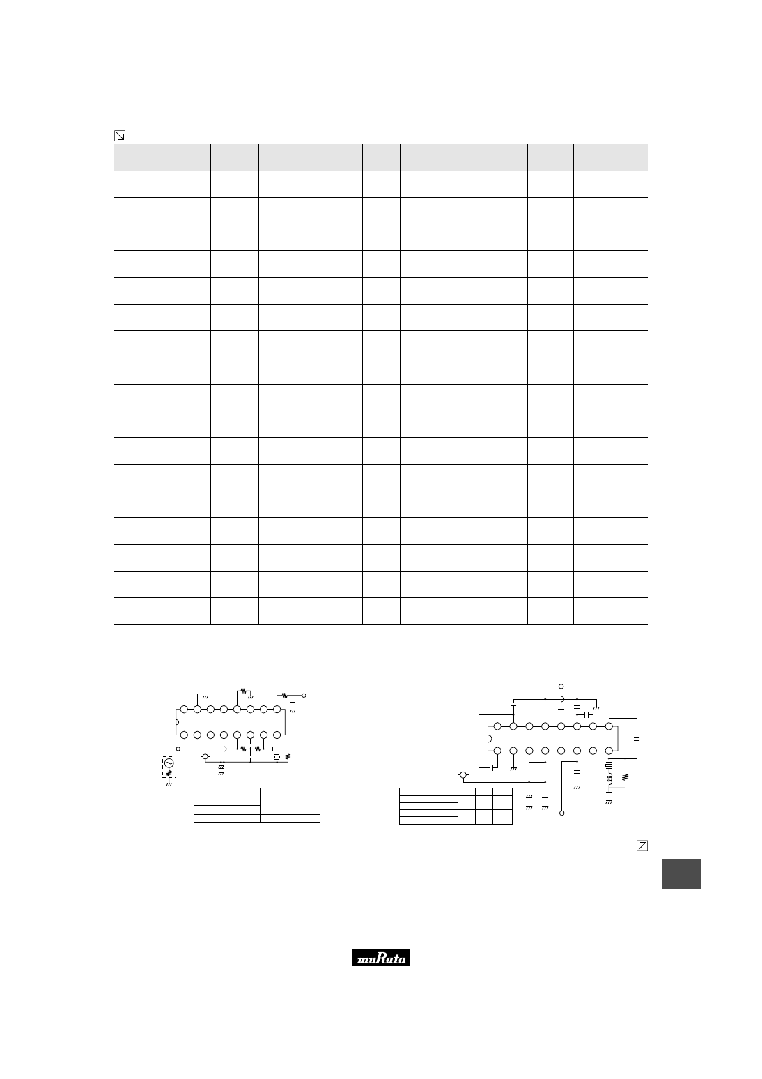
53
18
!
Note
• Please read rating and
!
CAUTION (for storage and operating, rating, soldering and mounting, handling) in this catalog to prevent smoking and/or burning, etc.
• This catalog has only typical specifications because there is no space for detailed specifications. Therefore, please approve our product specification or transact the approval sheet for product specification before ordering.
Part Number
Nominal Center
Frequency (fn)
(kHz)
Recovered
Audio 3dB BW
(kHz)
Recovered
Audio Output
(mV)
Distortion
(at fn)
(%)
Distortion
(%)
IC
IC Maker
Type
Continued from the preceding page.
CDBLB455KCAY07-B0
455
fn
±
4.0 min.
340
±
60
3.0 max.
-
MC3357
MOTOROLA
PLASTIC
CDBLB455KCAY13A-B0
455
fn
±
4.0 min.
350
±
50
3.0 max.
-
CXA1003BM
SONY
PLASTIC
CDBLB455KCAY21-B0
455
fn
±
4.0 min.
55
±
20
2.0 max.
-
TA31132
TOSHIBA
PLASTIC
CDBLB455KCAY24-B0
455
fn
±
4.0 min.
100
±
40
2.0 max.
-
TA31136
TOSHIBA
PLASTIC
CDBLB455KCAY28-B0
455
fn
±
4.0 min.
40
±
20
3.0 max.
-
TA31142FN
TOSHIBA
PLASTIC
CDBLB455KCAY32-B0
455
fn
±
4.0 min.
40
±
20
3.0 max.
-
TA31143
TOSHIBA
PLASTIC
CDBLB455KCAY34-B0
455
fn
±
4.0 min.
65
±
20
2.5 max.
-
MC13136
MOTOROLA
PLASTIC
CDBLB455KCAY40-B0
455
fn
±
4.0 min.
40
±
20
3.0 max.
-
TA31145
TOSHIBA
PLASTIC
CDBLB455KCAY42-B0
455
fn
±
4.0 min.
40
±
15
3.0 max.
-
TK14590
/TK14591
TOKO
PLASTIC
CDBLB455KCAY49-B0
455
fn
±
4.0 min.
45
±
10
3.0 max.
-
MC3361
MOTOROLA
PLASTIC
CDBLB455KCAY50-B0
455
fn
±
4.0 min.
64
±
6.4
4.0 max.
-
CXA3117N
SONY
PLASTIC
CDBLB455KCLY09-B0
455
fn
±
15.0 min.
70
±
20
1.5 max.
3.5 max.
[within fn
±
8kHz]
NE604N
PHILIPS
PLASTIC
CDBLB455KCLY13-B0
455
fn
±
15.0 min.
110
±
30
1.5 max.
5.0 max.
[within fn
±
8kHz]
CXA1003BM
SONY
PLASTIC
CDBLB455KCLY21-B0
455
fn
±
13.0 min.
65
±
20
2.5 max.
5.0 max.
[within fn
±
8kHz]
TA31132
TOSHIBA
PLASTIC
CDBLB455KCAX16-B0
455
fn
±
4.0 min.
185
±
40
2.0 max.
-
MC3372
MOTOROLA
PLASTIC
CDBLB455KCAX18-B0
455
fn
±
3.0 min.
180
±
40
2.0 max.
-
MC3371
MOTOROLA
PLASTIC
CDBLB455KCAX36-B0
455
fn
±
3.5 min.
100
±
25
3.5 max.
-
NE606
/616
PHILIPS
PLASTIC
■ Test Circuit
MC3357
AF output
Vcc
0.1
µ
0.01
µ
C
R
X
0.022
µ
FM S. S. G.
(Rg = 50
Ω
)
16
9
15
14
13
12
11
10
1
8
2
3
4
5
6
7
8.2k
10k
MC3357
50
0.1
µ
+
10
µ
47k
CDBLA455KCAY07-B0
CDBLB455KCAY07-B0
CDBCB455KCAY07-R0
Part Number (X)
C
R
150pF
150pF
1.5k
Ω
1.3k
Ω
Unit C
R
: F
:
Ω
NE604N
16
AF output
Vcc
0.1
µ
47
µ
C
R
X
1
0
0
p
0
.1
µ
100p
IF input
9
15
14
13
12
11
10
1
8
2
3
4
5
6
7
0
.0
1
µ
0.1
µ
+
1000p
L
0.01
µ
NE604
CDBLA455KCAY09-B0
CDBCB455KCAY09-R0
Part Number (X)
C
R
CDBLA455KCLY09-B0
CDBLB455KCLY09-B0
120pF 560
Ω
L
220
µ
H
120pF 1.8k
Ω
−
Unit C : F
R :
Ω
Continued on the following page.
Please read rating and
!
CAUTION (for storage and operating, rating, soldering and mounting, handling) in this PDF catalog to prevent smoking and/or burning, etc.
This catalog has only typical specifications. Therefore, you are requested to approve our product specification or to transact the approval sheet for product specificaion before ordering.
!
Note
P05E11.pdf 02.9.2
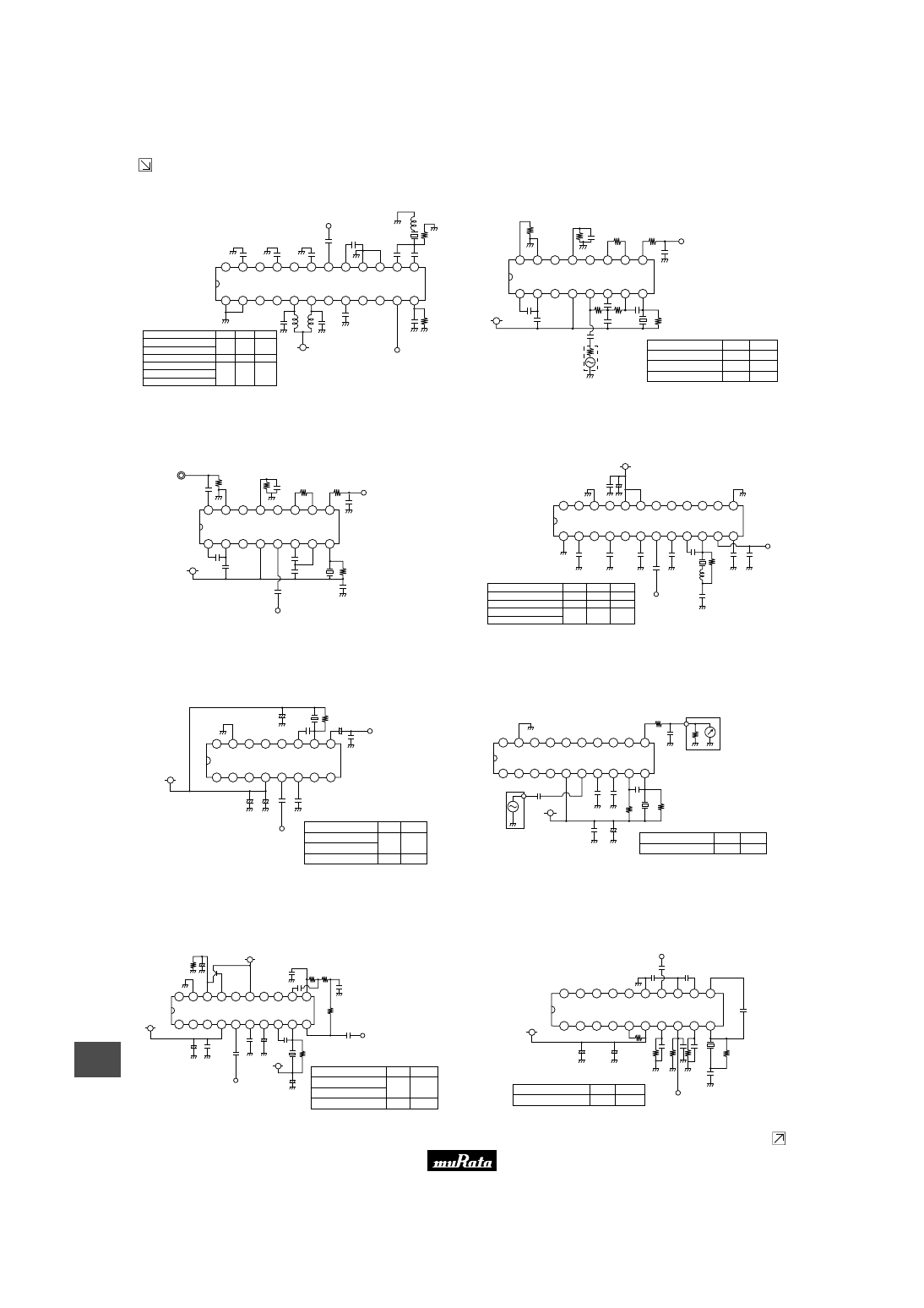
54
18
!
Note
• Please read rating and
!
CAUTION (for storage and operating, rating, soldering and mounting, handling) in this catalog to prevent smoking and/or burning, etc.
• This catalog has only typical specifications because there is no space for detailed specifications. Therefore, please approve our product specification or transact the approval sheet for product specification before ordering.
Continued from the preceding page.
■ Test Circuit
CXA1003BM
24
AF output
Vcc
0.01
µ
C
R
X
0
.0
1
µ
100
µ
CXA1003BM
2
7
0
0
p
51k
0.01
µ
0.01
µ
0.01
µ
0.01
µ
0.01
µ
L
100
µ
0.01
µ
13
14
15
16
17
18
19
20
21
22
23
1
12
11
10
9
8
7
6
5
4
3
2
0.01
µ
CDBLA455KCAY13A-B0
CDBLB455KCAY13A-B0
CDBCB455KCAY13-R0
Part Number (X)
C
R
82pF
82pF
1.2k
Ω
1.0k
Ω
CDBLA455KCLY13-B0
CDBLB455KCLY13-B0
CDBCB455KCLY13-R0
82pF 560
Ω
L
220
µ
H
−
−
IF input
Unit C : F
R :
Ω
MC3372
AF output
Unit C : F
R :
Ω
Vcc
16
15
14
13
12
11
10
9
1
2
3
4
5
6
7
8
0.01
µ
51
51k
0.1
µ
510k
8.2k
0.01
µ
R
51k
1.8k
0.1
µ
C
0.01
µ
0.1
µ
(Rg = 50
Ω
)
FM S. S. G
220p
68p
MC3372
X
CDBLA455KCAX16-B0
CDBLB455KCAX16-B0
CDBCB455KCAY16-R0
Part Number (X)
C
R
100pF
27pF
100pF
1.3k
Ω
4.3k
Ω
1.0k
Ω
MC3371
AF output
Unit C
R
: F
:
Ω
RF input
16
9
15
14
13
12
11
10
1
8
2
3
4
5
6
7
0.01
µ
51
51k
0.1
µ
510k
8.2k
0.01
µ
0
.1
µ
0.1
µ
0.01
µ
IF input
68p
220p
R
X
Test condition
Vcc =
+
6.0V
R = 6.2k
Ω
X : CDBLB455KCAX18-B0
MC3371
Vcc
TA31132
24
AF
output
Vcc
10n
100
µ
13
14
15
16
17
18
19
20
21
22
23
1
12
11
10
9
8
7
6
5
4
3
2
TA31132
22n 22n
22n
22n
10n
IF input
10n
X
R
L
0.1
µ
C
1n
CDBLB455KCAY21-B0
CDBCB455KCAY21-R0
Part Number (X)
C
R
100pF
100pF
1.5k
Ω
1.2k
Ω
CDBLB455KCLY21-B0
CDBCB455KCLY21-R0
100pF
680
Ω
L
220
µ
H
−
−
Unit C : F
R :
Ω
TA31136
AF output
Vcc
(
+
2.0V)
10
µ
+
X
R
1
µ
0.01
µ
C
0
.1
µ
0
.0
1
µ
0
.1
µ
10
µ
+
+
TA31136F
16
9
15
14
13
12
11
10
1
8
2
3
4
5
6
7
IF input
CDBLA455KCAY24-B0
CDBLB455KCAY24-B0
CDBCB455KCAY24-R0
Part Number (X)
C
R
91pF
91pF
1.5k
Ω
1.2k
Ω
Unit C : F
R :
Ω
TK10487
20
19
18
17
16
15
14
13
12
1
R
C
2k
Vcc
TK10487
0.01
µ
10
µ
+
0
.1
µ
0
.1
µ
0
.0
1
µ
0
.0
1
µ
8.2k
2
3
4
5
6
7
8
9
11
10
X
CDBCB455KCAY27-R0
Part Number (X)
C
R
33pF
1.0k
Ω
Unit C : F
R :
Ω
TA31142
20
AF
output
Vcc
11
12
13
14
15
16
17
18
19
1
10
9
8
7
6
5
4
3
2
430
+
2.2
µ
Vcc
560p
68k 68k
3300p
68k
0.01
µ
R
10
µ
IF input
0.01
µ
0
.1
µ
1
0
µ
+
+
+
10
µ
0.1
µ
2SC1048
0.01
µ
TA31142F
X
C
Vcc
CDBLA455KCAY28-B0
CDBLB455KCAY28-B0
CDBCB455KCAY28-R0
Part Number (X)
C
R
22pF
22pF
3.3k
Ω
2.7k
Ω
Unit C : F
R :
Ω
NE605
20
AF output
Vcc
+
0.1
µ
0.01
µ
C
0.1
µ
R
X
0.1
µ
1
5
0
p
5
n
0
.1
µ
1
0
0
k
1
0
0
k
22k
0.1
µ
22
µ
NE605
11
12
13
14
15
16
17
18
19
1
10
9
8
7
6
5
4
3
2
IF input
1
0
0
k
CDBCB455KCAY29-R0
Part Number (X)
C
R
56pF
2.2k
Ω
Unit C : F
R :
Ω
Continued on the following page.
Please read rating and
!
CAUTION (for storage and operating, rating, soldering and mounting, handling) in this PDF catalog to prevent smoking and/or burning, etc.
This catalog has only typical specifications. Therefore, you are requested to approve our product specification or to transact the approval sheet for product specificaion before ordering.
!
Note
P05E11.pdf 02.9.2
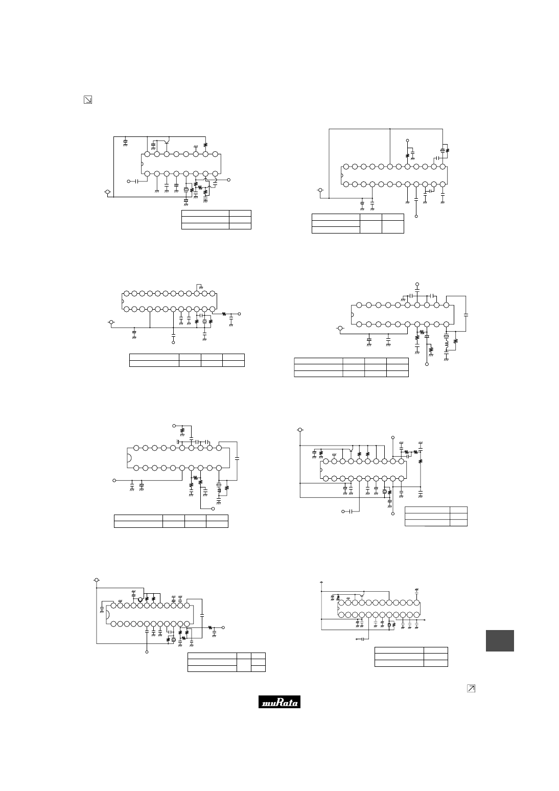
55
18
!
Note
• Please read rating and
!
CAUTION (for storage and operating, rating, soldering and mounting, handling) in this catalog to prevent smoking and/or burning, etc.
• This catalog has only typical specifications because there is no space for detailed specifications. Therefore, please approve our product specification or transact the approval sheet for product specification before ordering.
Continued from the preceding page.
■ Test Circuit
TA31143
AF output
Vcc
0.1
µ
100
µ
R
X
0.1
µ
TA31143
16
9
10
11
12
13
14
15
1
8
7
6
5
4
3
2
10
µ
+
+
+
IF input
3300p
560p
68k
10
µ
68k
2SA1015
1.2k
68k
+
0.01
µ
2.2
µ
CDBLB455KCAY32-B0
CDBCB455KCAY32-R0
Part Number (X)
R
3.3k
Ω
2.7k
Ω
Unit C : F
R :
Ω
MC13136
24
1
23
2
22
3
21
4
20
5
19
6
18
7
17
8
16
9
15
10
14
11
13
12
R
X
C
Vcc
MC13136
0.01
µ
0.01
µ
0.15
µ
1k
0.1
µ
IF input
AF input
0.1
µ
0.1
µ
0.1
µ
+
CDBLA455KCAY34-B0
CDBLB455KCAY34-B0
Part Number (X)
C
R
100pF
1.2k
Ω
Unit C
R
: F
:
Ω
TK10930
24
1
23
2
22
3
21
4
20
5
19
6
18
7
17
8
16
9
15
10
14
11
13
12
R2
R1
C
X
Vcc
AF
output
IF input
TK10930
0.01
µ
0.1
µ
0.1
µ
10
µ
+
0.1
µ
0.1
µ
8.2k
CDBCB455KCAY35-R0
Part Number (X)
R1
R2
2.0k
Ω
1.0k
Ω
C
33pF
Unit C : F
R :
Ω
NE(SA)606/616
20
1
19
2
18
3
17
4
16
5
15
6
14
7
13
8
12
9
11
10
R
X
L
IF input
AF output
C
20k
2k
8.2k
Vcc
NE606 or NE616
0.1
µ
0.1
µ
0.1
µ
0.01
µ
0.1
µ
0.1
µ
2.2
µ
+
2.2
µ
+
CDBLB455KCAX36-B0
CDBCB455KCLX36-R0
Part Number (X)
C
R
22pF
27pF
4.7k
Ω
2.2k
Ω
L
−
1mH
Unit C : F
R :
Ω
NE(SA)607/617
20
AF output
Vcc
0.1
µ
0.01
µ
0.01
µ
C
R
X
L
0.1
µ
0.01
µ
51
IF input
11
19
18
17
16
15
14
13
12
1
10
2
3
4
5
6
7
8
9
22k
1.5k
NE607/617 (PHILIPS)
8.2k
+10
µ
0.1
µ
0.1
µ
CDBCB455KCLX39-R0
Part Number (X)
C
R
22pF
2.7k
Ω
L
1mH
Unit C : F
R :
Ω
L : H
TA31145
AF output
0.1
µ
R
X
0.1
µ
1000p
100k
10
µ
IF input
3300p
Vcc
0.1
µ
20
+
+
10
µ
5600p
100k
+
2.2
µ
430
+
0.01
µ
68k
68k
68k
560p
TA31145 (TOSHIBA)
11
19
18
17
16
15
14
13
12
1
10
2
3
4
5
6
7
8
9
CDBLB455KCAY40-B0
CDBCB455KCAY40-R0
Part Number (X)
R
3.3k
Ω
2.7k
Ω
Unit C : F
R :
Ω
TK14590/14591
AF
output
Vcc
(1.3V)
0.1
µ
0.01
µ
C
R
0.0033
µ
100k
X
IF input
24
13
14
15
16
17
18
19
20
21
22
23
1
12
11
10
9
8
7
6
5
4
3
2
100k
8.2k
0.01
µ
560p
100k
0.1
µ
0.1
µ
0.01
µ
1
µ
TK14590V (TOKO)
0.01
µ
0.15
µ
100k
100k
CDBLA455KCAY42-B0
CDBCB455KCAY42-R0
3.3k
Ω
2.7k
Ω
Part Number (X)
C
R
22pF
Unit C : F
R :
Ω
TA31147
24
22
20 19
16 15 14 13
17
18
21
23
1
3
5
6
9 10 11 12
8
7
4
2
1200p
1000p
10
µ
10
µ
0.1
µ
0.01
µ
2.2
µ
0.1
µ
0.1
µ
1200p
820p
R
X
W
W
W
IF
input
AF
output
Vcc
TA31147(TOSHIBA)
430
Part Number (X)
CDBLB455KCAY47-B0
CDBCB455KCAY47-R0
R
3.3k
Ω
2.7k
Ω
Unit C : F
R :
Ω
Continued on the following page.
Please read rating and
!
CAUTION (for storage and operating, rating, soldering and mounting, handling) in this PDF catalog to prevent smoking and/or burning, etc.
This catalog has only typical specifications. Therefore, you are requested to approve our product specification or to transact the approval sheet for product specificaion before ordering.
!
Note
P05E11.pdf 02.9.2
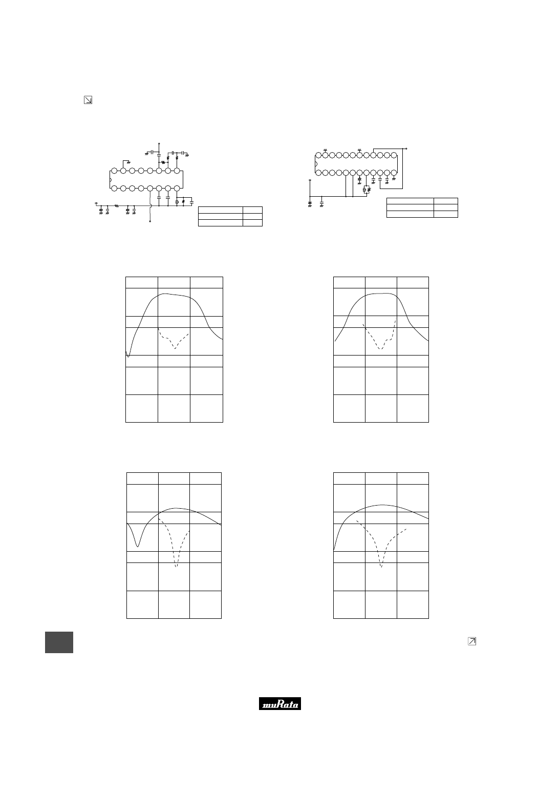
56
18
!
Note
• Please read rating and
!
CAUTION (for storage and operating, rating, soldering and mounting, handling) in this catalog to prevent smoking and/or burning, etc.
• This catalog has only typical specifications because there is no space for detailed specifications. Therefore, please approve our product specification or transact the approval sheet for product specification before ordering.
Continued from the preceding page.
■ Test Circuit
MC3361
47
µ
0.01
µ
0.1
µ
Vcc
16
15
14
13
12
11
10
9
1
2
3
4
5
6
7
1
µ
22
MC3361
100p
1000p
0.1
µ
0.1
µ
150k
100k
AF output
1k
R
X
IF input
0.022
µ
0.1
µ
0.1
µ
8
Part Number (X)
CDBLB455KCAY49-B0
CDBCB455KCAY49-R0
R
1.8k
Ω
1.5k
Ω
Unit C
R
: F
:
Ω
CXA3117
24
22
20 19
16 15 14 13
17
21
23
1
3
5
6
9 10 11 12
8
7
4
2
1
2
0
0
p
1
µ
33
µ
0.01
µ
1200p
1200p
R
X
AF out
Vcc
CXA3117(SONY)
18
Part Number (X)
CDBLB455KCAY50-B0
CDBCB455KCAY50-R0
R
8.2k
Ω
6.2k
Ω
Unit C
R
: F
:
Ω
■ Recovered Audio Curve Specification
CDBCB455KCAY07-R0
500
A
F
O
u
tp
u
t
V
o
lt
a
g
e
(
m
V
)
T
.H
.D
.
(%
)
440
450
460
470
Frequency (kHz)
50.0
100
10.0
50
5.0
10
1.0
5
0.5
1
0.1
CDBLA/CDBLB455KCAY07-B0
500
A
F
O
u
tp
u
t
V
o
lt
a
g
e
(
m
V
)
T
.H
.D
.
(%
)
440
450
460
470
Frequency (kHz)
50.0
100
10.0
50
5.0
10
1.0
5
0.5
1
0.1
CDBCB455KCAY09-R0
500
A
F
O
u
tp
u
t
V
o
lt
a
g
e
(
m
V
)
T
.H
.D
.
(%
)
440
450
460
470
Frequency (kHz)
50.0
100
10.0
50
5.0
10
1.0
5
0.5
1
0.1
CDBLA455KCAY09-B0
500
A
F
O
u
tp
u
t
V
o
lt
a
g
e
(
m
V
)
T
.H
.D
.
(%
)
440
450
460
470
Frequency (kHz)
50.0
100
10.0
50
5.0
10
1.0
5
0.5
1
0.1
Continued on the following page.
Please read rating and
!
CAUTION (for storage and operating, rating, soldering and mounting, handling) in this PDF catalog to prevent smoking and/or burning, etc.
This catalog has only typical specifications. Therefore, you are requested to approve our product specification or to transact the approval sheet for product specificaion before ordering.
!
Note
P05E11.pdf 02.9.2
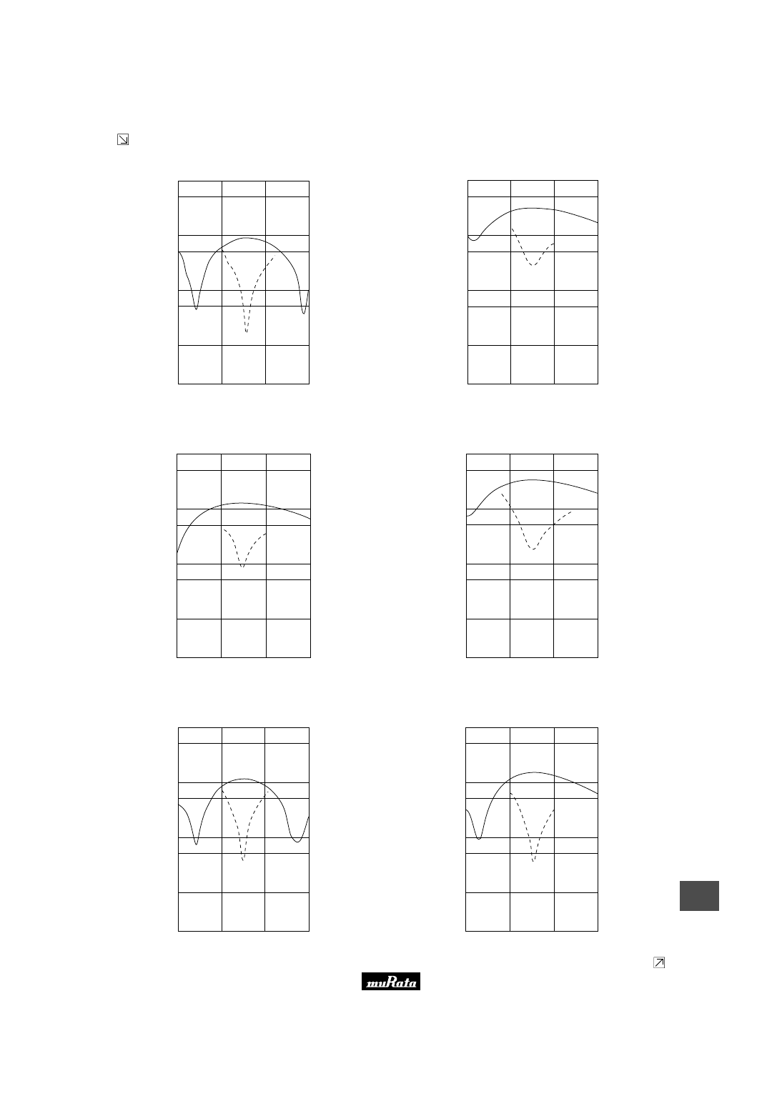
57
18
!
Note
• Please read rating and
!
CAUTION (for storage and operating, rating, soldering and mounting, handling) in this catalog to prevent smoking and/or burning, etc.
• This catalog has only typical specifications because there is no space for detailed specifications. Therefore, please approve our product specification or transact the approval sheet for product specification before ordering.
Continued from the preceding page.
■ Recovered Audio Curve Specification
CDBLA/CDBLB455KCLY09-B0
500
A
F
O
u
tp
u
t
V
o
lt
a
g
e
(
m
V
)
T
.H
.D
.
(%
)
395
435
475
515
Frequency (kHz)
50.0
100
10.0
50
5.0
10
1.0
5
0.5
1
0.1
CDBCB455KCAY13-R0
500
A
F
O
u
tp
u
t
V
o
lt
a
g
e
(
m
V
)
T
.H
.D
.
(%
)
440
450
460
470
Frequency (kHz)
50.0
100
10.0
50
5.0
10
1.0
5
0.5
1
0.1
CDBCB455KCLY13-R0
A
F
O
u
tp
u
t
V
o
lt
a
g
e
(
m
V
)
425
445
465
485
Frequency (kHz)
500
100
50
10
5
1
T
.H
.D
.
(%
)
50.0
10.0
5.0
1.0
0.5
0.1
CDBLA/CDBLB455KCAY13A-B0
500
A
F
O
u
tp
u
t
V
o
lt
a
g
e
(
m
V
)
T
.H
.D
.
(%
)
440
450
460
470
Frequency (kHz)
50.0
100
10.0
50
5.0
10
1.0
5
0.5
1
0.1
CDBLA/CDBLB455KCLY13-B0
500
A
F
O
u
tp
u
t
V
o
lt
a
g
e
(
m
V
)
T
.H
.D
.
(%
)
395
435
475
515
Frequency (kHz)
50.0
100
10.0
50
5.0
10
1.0
5
0.5
1
0.1
CDBCB455KCAY16-R0
A
F
O
u
tp
u
t
V
o
lt
a
g
e
(
m
V
)
440
450
460
470
Frequency (kHz)
500
100
50
10
5
1
T
.H
.D
.
(%
)
50.0
10.0
5.0
1.0
0.5
0.1
Continued on the following page.
Please read rating and
!
CAUTION (for storage and operating, rating, soldering and mounting, handling) in this PDF catalog to prevent smoking and/or burning, etc.
This catalog has only typical specifications. Therefore, you are requested to approve our product specification or to transact the approval sheet for product specificaion before ordering.
!
Note
P05E11.pdf 02.9.2
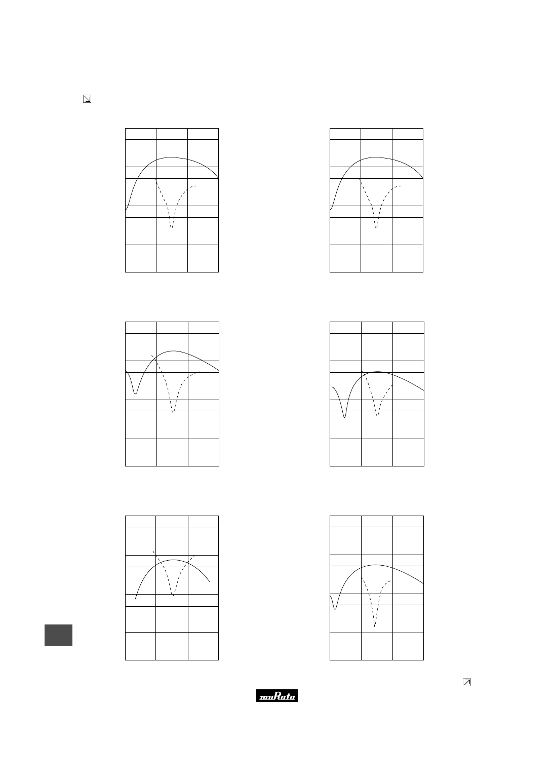
58
18
!
Note
• Please read rating and
!
CAUTION (for storage and operating, rating, soldering and mounting, handling) in this catalog to prevent smoking and/or burning, etc.
• This catalog has only typical specifications because there is no space for detailed specifications. Therefore, please approve our product specification or transact the approval sheet for product specification before ordering.
Continued from the preceding page.
■ Recovered Audio Curve Specification
CDBLA455KCAY16-B0
A
F
O
u
tp
u
t
V
o
lt
a
g
e
(
m
V
)
440
450
460
470
Frequency (kHz)
500
100
50
10
5
1
T
.H
.D
.
(%
)
50.0
10.0
5.0
1.0
0.5
0.1
CDBLB455KCAX16-B0
A
F
O
u
tp
u
t
V
o
lt
a
g
e
(
m
V
)
440
450
460
470
Frequency (kHz)
500
100
50
10
5
1
T
.H
.D
.
(%
)
50.0
10.0
5.0
1.0
0.5
0.1
CDBLB455KCAX18-B0
A
F
O
u
tp
u
t
V
o
lt
a
g
e
(
m
V
)
440
450
460
470
Frequency (kHz)
500
100
50
10
5
1
T
.H
.D
.
(%
)
50.0
10.0
5.0
1.0
0.5
0.1
CDBCB455KCAY21-R0
A
F
O
u
tp
u
t
V
o
lt
a
g
e
(
m
V
)
440
450
460
470
Frequency (kHz)
500
100
50
10
5
1
T
.H
.D
.
(%
)
50.0
10.0
5.0
1.0
0.5
0.1
CDBCB455KCLY21-R0
A
F
O
u
tp
u
t
V
o
lt
a
g
e
(
m
V
)
410
440
470
500
Frequency (kHz)
500
100
50
10
5
1
T
.H
.D
.
(%
)
50.0
10.0
5.0
1.0
0.5
0.1
CDBLB455KCAY21-B0
A
F
O
u
tp
u
t
V
o
lt
a
g
e
(
m
V
)
440
450
460
470
Frequency (kHz)
500
100
50
10
5
1
T
.H
.D
.
(%
)
50.0
10.0
5.0
1.0
0.5
0.1
Continued on the following page.
Please read rating and
!
CAUTION (for storage and operating, rating, soldering and mounting, handling) in this PDF catalog to prevent smoking and/or burning, etc.
This catalog has only typical specifications. Therefore, you are requested to approve our product specification or to transact the approval sheet for product specificaion before ordering.
!
Note
P05E11.pdf 02.9.2
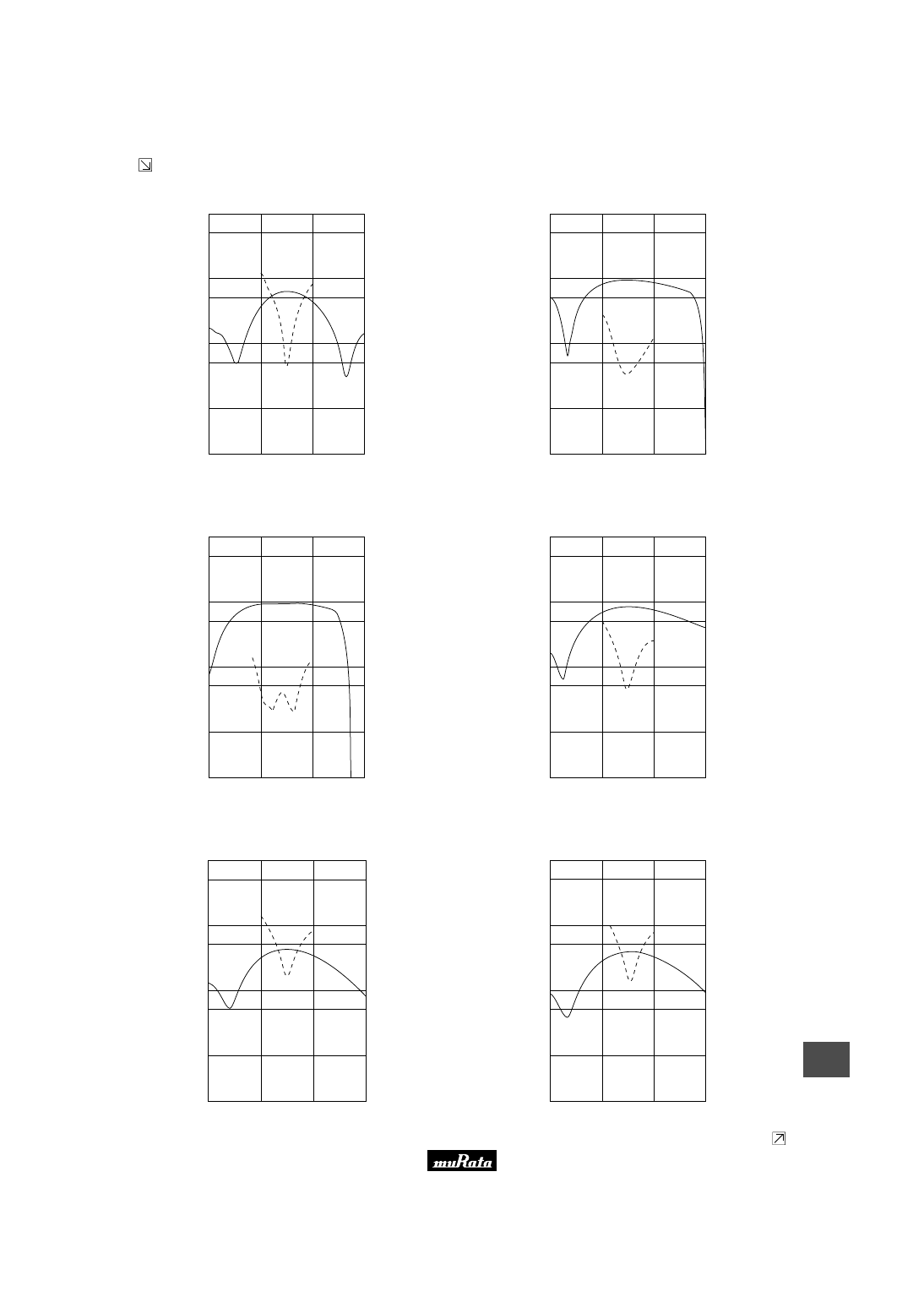
59
18
!
Note
• Please read rating and
!
CAUTION (for storage and operating, rating, soldering and mounting, handling) in this catalog to prevent smoking and/or burning, etc.
• This catalog has only typical specifications because there is no space for detailed specifications. Therefore, please approve our product specification or transact the approval sheet for product specification before ordering.
Continued from the preceding page.
■ Recovered Audio Curve Specification
CDBLB455KCLY21-B0
A
F
O
u
tp
u
t
V
o
lt
a
g
e
(
m
V
)
395
435
475
515
Frequency (kHz)
500
100
50
10
5
1
T
.H
.D
.
(%
)
50.0
10.0
5.0
1.0
0.5
0.1
CDBCB455KCAY24-R0
A
F
O
u
tp
u
t
V
o
lt
a
g
e
(
m
V
)
440
450
460
470
Frequency (kHz)
500
100
50
10
5
1
T
.H
.D
.
(%
)
50.0
10.0
5.0
1.0
0.5
0.1
CDBLA/CDBLB455KCAY24-B0
A
F
O
u
tp
u
t
V
o
lt
a
g
e
(
m
V
)
440
450
460
470
Frequency (kHz)
500
100
50
10
5
1
T
.H
.D
.
(%
)
50.0
10.0
5.0
1.0
0.5
0.1
CDBCB455KCAY27-R0
A
F
O
u
tp
u
t
V
o
lt
a
g
e
(
m
V
)
440
450
460
470
Frequency (kHz)
500
100
50
10
5
1
T
.H
.D
.
(%
)
50.0
10.0
5.0
1.0
0.5
0.1
CDBCB455KCAY28-R0
A
F
O
u
tp
u
t
V
o
lt
a
g
e
(
m
V
)
440
450
460
470
Frequency (kHz)
500
100
50
10
5
1
T
.H
.D
.
(%
)
50.0
10.0
5.0
1.0
0.5
0.1
CDBLA/CDBLB455KCAY28-B0
A
F
O
u
tp
u
t
V
o
lt
a
g
e
(
m
V
)
440
450
460
470
Frequency (kHz)
500
100
50
10
5
1
T
.H
.D
.
(%
)
50.0
10.0
5.0
1.0
0.5
0.1
Continued on the following page.
Please read rating and
!
CAUTION (for storage and operating, rating, soldering and mounting, handling) in this PDF catalog to prevent smoking and/or burning, etc.
This catalog has only typical specifications. Therefore, you are requested to approve our product specification or to transact the approval sheet for product specificaion before ordering.
!
Note
P05E11.pdf 02.9.2
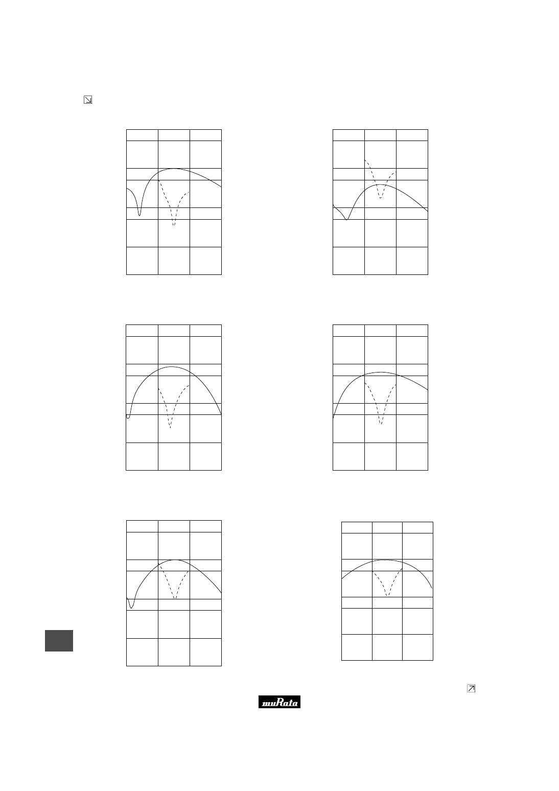
60
18
!
Note
• Please read rating and
!
CAUTION (for storage and operating, rating, soldering and mounting, handling) in this catalog to prevent smoking and/or burning, etc.
• This catalog has only typical specifications because there is no space for detailed specifications. Therefore, please approve our product specification or transact the approval sheet for product specification before ordering.
Continued from the preceding page.
■ Recovered Audio Curve Specification
CDBCB455KCAY29-R0
A
F
O
u
tp
u
t
V
o
lt
a
g
e
(
m
V
)
440
450
460
470
Frequency (kHz)
500
100
50
10
5
1
T
.H
.D
.
(%
)
50.0
10.0
5.0
1.0
0.5
0.1
CDBCB455KCAY32-R0
A
F
O
u
tp
u
t
V
o
lt
a
g
e
(
m
V
)
440
450
460
470
Frequency (kHz)
500
100
50
10
5
1
T
.H
.D
.
(%
)
50.0
10.0
5.0
1.0
0.5
0.1
CDBLB455KCAY32-B0
A
F
O
u
tp
u
t
V
o
lt
a
g
e
(
m
V
)
440
450
460
470
Frequency (kHz)
500
100
50
10
5
1
T
.H
.D
.
(%
)
50.0
10.0
5.0
1.0
0.5
0.1
CDBLA/CDBLB455KCAY34-B0
A
F
O
u
tp
u
t
V
o
lt
a
g
e
(
m
V
)
440
450
460
470
Frequency (kHz)
500
100
50
10
5
1
T
.H
.D
.
(%
)
50.0
10.0
5.0
1.0
0.5
0.1
CDBCB455KCAY35-R0
A
F
O
u
tp
u
t
V
o
lt
a
g
e
(
m
V
)
440
450
460
470
Frequency (kHz)
500
100
50
10
5
1
T
.H
.D
.
(%
)
50.0
10.0
5.0
1.0
0.5
0.1
CDBCB455KCLX36-R0
A
F
O
u
tp
u
t
V
o
lt
a
g
e
(
m
V
)
T
.H
.D
.
(%
)
Frequency ( kHz )
1
10
100
500
425
445
465
486
0.1
0.5
5
50
5
50
1
10
Continued on the following page.
Please read rating and
!
CAUTION (for storage and operating, rating, soldering and mounting, handling) in this PDF catalog to prevent smoking and/or burning, etc.
This catalog has only typical specifications. Therefore, you are requested to approve our product specification or to transact the approval sheet for product specificaion before ordering.
!
Note
P05E11.pdf 02.9.2
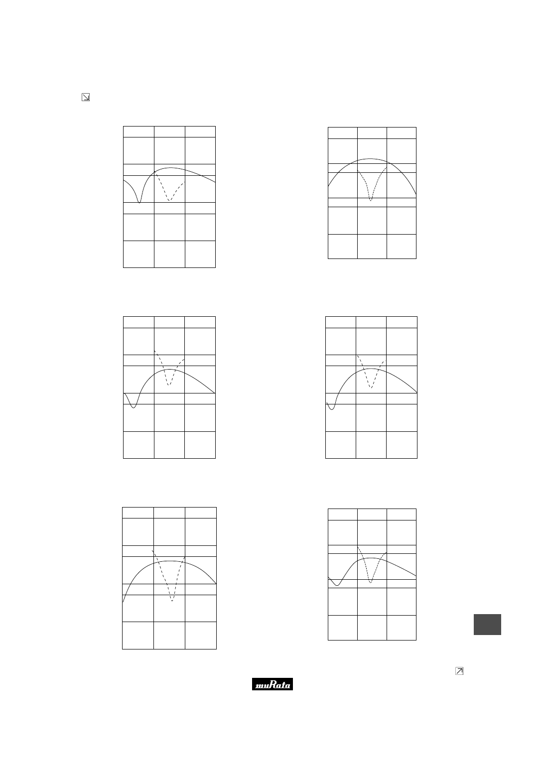
61
18
!
Note
• Please read rating and
!
CAUTION (for storage and operating, rating, soldering and mounting, handling) in this catalog to prevent smoking and/or burning, etc.
• This catalog has only typical specifications because there is no space for detailed specifications. Therefore, please approve our product specification or transact the approval sheet for product specification before ordering.
Continued from the preceding page.
■ Recovered Audio Curve Specification
CDBLB455KCAX36-B0
A
F
O
u
tp
u
t
V
o
lt
a
g
e
(
m
V
)
440
450
460
470
Frequency (kHz)
500
100
50
10
5
1
T
.H
.D
.
(%
)
50.0
10.0
5.0
1.0
0.5
0.1
CDBCB455KCLX39-R0
Frequency (kHz)
425
445
465
485
500
100
50
10
5
1
50.0
10.0
5.0
1.0
0.5
0.1
A
F
O
u
tp
u
t
V
o
lt
a
g
e
(
m
V
)
T
.
H
.
D
.
(%
)
CDBCB455KCAY40-R0
500
A
F
O
u
tp
u
t
V
o
lt
a
g
e
(
m
V
)
T
.H
.D
.
(%
)
440
450
460
470
Frequency (kHz)
50.0
100
10.0
50
5.0
10
1.0
5
0.5
1
0.1
CDBLB455KCAY40-B0
500
A
F
O
u
tp
u
t
V
o
lt
a
g
e
(
m
V
)
T
.H
.D
.
(%
)
440
450
460
470
Frequency (kHz)
50.0
100
10.0
50
5.0
10
1.0
5
0.5
1
0.1
CDBLA/CDBLB455KCAY42-B0
500
A
F
O
u
tp
u
t
V
o
lt
a
g
e
(
m
V
)
T
.H
.D
.
(%
)
440
450
460
470
Frequency (kHz)
50.0
100
10.0
50
5.0
10
1.0
5
0.5
1
0.1
CDBCB455KCAY49-R0
Frequency (kHz)
A
F
O
u
tp
u
t
V
o
lt
a
g
e
(
m
V
)
T
.
H
.
D
.
(%
)
440
450
460
470
500
100
50
10
5
1
50.0
10.0
5.0
1.0
0.5
0.1
Continued on the following page.
Please read rating and
!
CAUTION (for storage and operating, rating, soldering and mounting, handling) in this PDF catalog to prevent smoking and/or burning, etc.
This catalog has only typical specifications. Therefore, you are requested to approve our product specification or to transact the approval sheet for product specificaion before ordering.
!
Note
P05E11.pdf 02.9.2
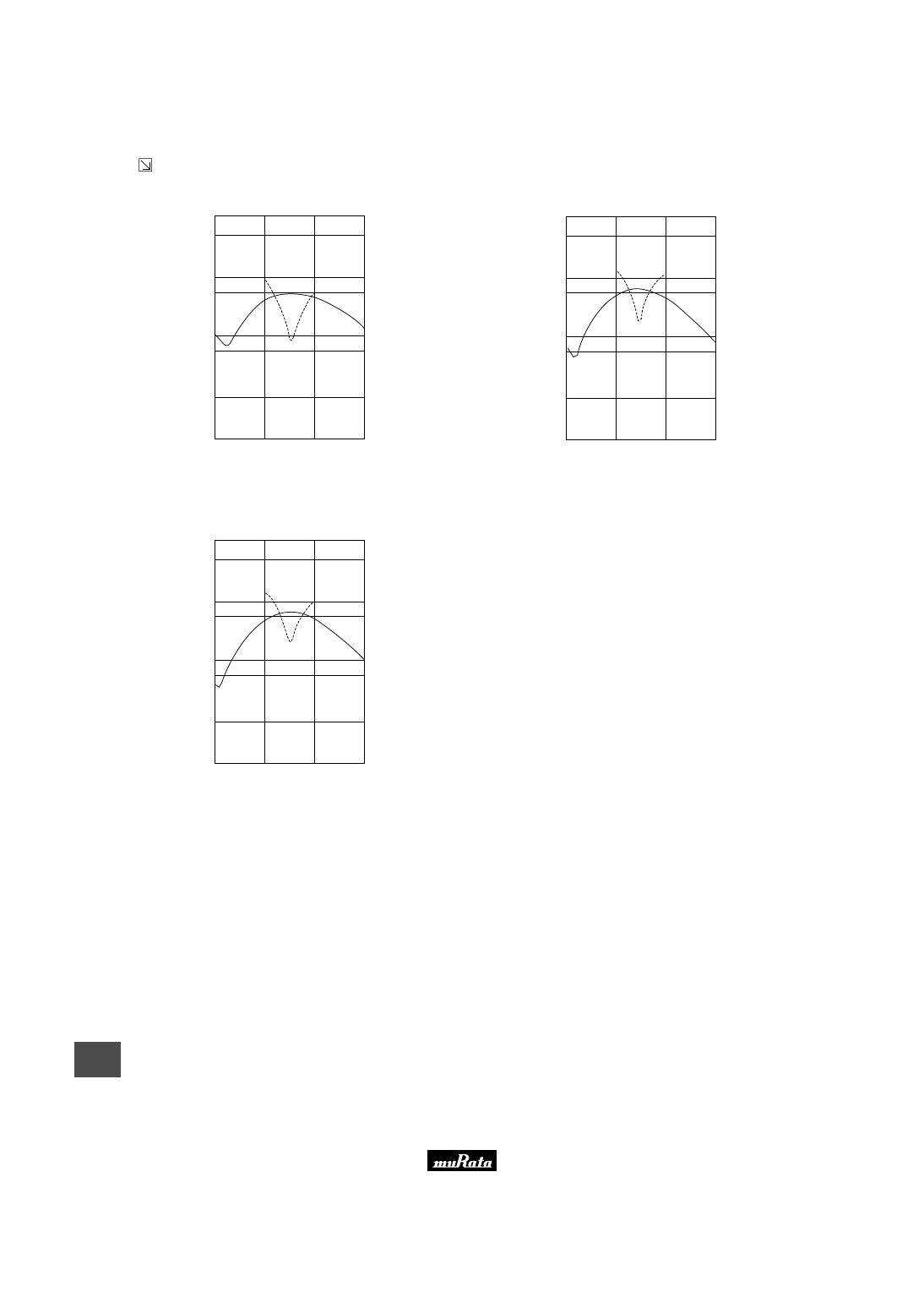
62
18
!
Note
• Please read rating and
!
CAUTION (for storage and operating, rating, soldering and mounting, handling) in this catalog to prevent smoking and/or burning, etc.
• This catalog has only typical specifications because there is no space for detailed specifications. Therefore, please approve our product specification or transact the approval sheet for product specification before ordering.
Continued from the preceding page.
■ Recovered Audio Curve Specification
CDBLB455KCAY49-B0
Frequency (kHz)
A
F
O
u
tp
u
t
V
o
lt
a
g
e
(
m
V
)
T
.
H
.
D
.
(%
)
440
450
460
470
500
100
50
10
5
1
50.0
10.0
5.0
1.0
0.5
0.1
CDBCB455KCAY50-R0
Frequency (kHz)
A
F
O
u
tp
u
t
V
o
lt
a
g
e
(
m
V
)
T
.
H
.
D
.
(%
)
440
450
460
470
500
100
50
10
5
1
50.0
10.0
5.0
1.0
0.5
0.1
CDBLB455KCAY50-B0
Frequency (kHz)
A
F
O
u
tp
u
t
V
o
lt
a
g
e
(
m
V
)
T
.
H
.
D
.
(%
)
440
450
460
470
500
100
50
10
5
1
50.0
10.0
5.0
1.0
0.5
0.1
Please read rating and
!
CAUTION (for storage and operating, rating, soldering and mounting, handling) in this PDF catalog to prevent smoking and/or burning, etc.
This catalog has only typical specifications. Therefore, you are requested to approve our product specification or to transact the approval sheet for product specificaion before ordering.
!
Note
P05E11.pdf 02.9.2
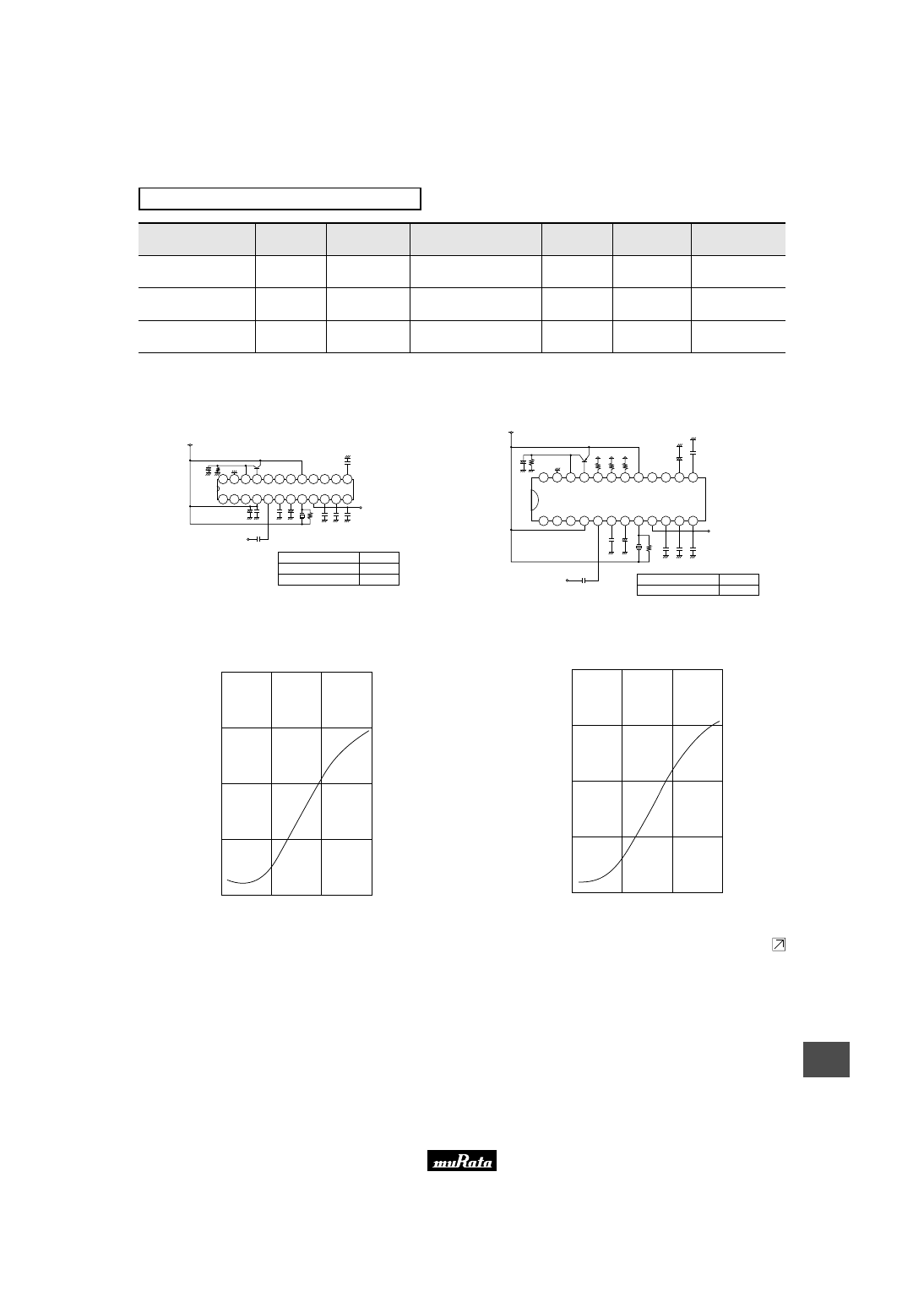
63
18
!
Note
• Please read rating and
!
CAUTION (for storage and operating, rating, soldering and mounting, handling) in this catalog to prevent smoking and/or burning, etc.
• This catalog has only typical specifications because there is no space for detailed specifications. Therefore, please approve our product specification or transact the approval sheet for product specification before ordering.
Specified by S Curve Characteristics
Part Number
Nominal Center
Frequency (fn)
(kHz)
S Curve (1)
Output Volt. at fn
(mV)
S Curve (2)
at fn
±
4.8kHz
(mV)
IC
IC Maker
Type
CDBCB455KCAY47-R0
455
130
±
20
150
±
15
TA31147
TOSHIBA
SMD
CDBCB455KCAY54-R0
455
165
±
20
170
±
20
TA31149
TOSHIBA
SMD
CDBLB455KCAY47-B0
455
140
±
20
150
±
15
TA31147
TOSHIBA
PLASTIC
■ Test Circuit
TA31147
24
22
20 19
16 15 14 13
17
18
21
23
1
3
5
6
9 10 11 12
8
7
4
2
1
2
0
0
p
1000p
1
0
µ
10
µ
0.1
µ
0.01
µ
2.2
µ
0
.1
µ
0
.1
µ
1
2
0
0
p
8
2
0
p
R
X
W
W
W
IF
input
AF
output
Vcc
TA31147(TOSHIBA)
430
Part Number (X)
CDBLB455KCAY47-B0
CDBCB455KCAY47-R0
R
3.3k
Ω
2.7k
Ω
Unit C : F
R :
Ω
TA31149
24
22
16
15
1
3
5
9
7
4
2
1
0
0
0
p
1
0
µ
0
.1
µ
10
µ
1
0
0
0
p
1
0
0
k
0.1
µ
R
X
A
F
o
u
tp
u
t
1
2
0
0
p
1
5
0
0
p
Vcc (
W
1.4V)
TA31149(TOSHIBA)
12
11
8
10
6
IF
input
17
2
.2
µ
430
23
21
20
Vcc
1
0
0
k
Vcc
1
0
0
k
Vcc
19
18
14
13
+
+
+
Part Number (X)
CDBCB455KCAY54-R0
R
2.7k
Ω
Unit C : F
R :
Ω
■ S Curve Specification
CDBCB455KCAY47-R0
440
450
460
470
0.0
0.1
0.2
0.3
0.4
Frequency (kHz)
V
o
lt
(
V
)
CDBLB455KCAY47-B0
Frequency (kHz)
440
450
460
470
0.0
0.1
0.2
0.3
0.4
V
o
lt
(
V
)
Continued on the following page.
Please read rating and
!
CAUTION (for storage and operating, rating, soldering and mounting, handling) in this PDF catalog to prevent smoking and/or burning, etc.
This catalog has only typical specifications. Therefore, you are requested to approve our product specification or to transact the approval sheet for product specificaion before ordering.
!
Note
P05E11.pdf 02.9.2
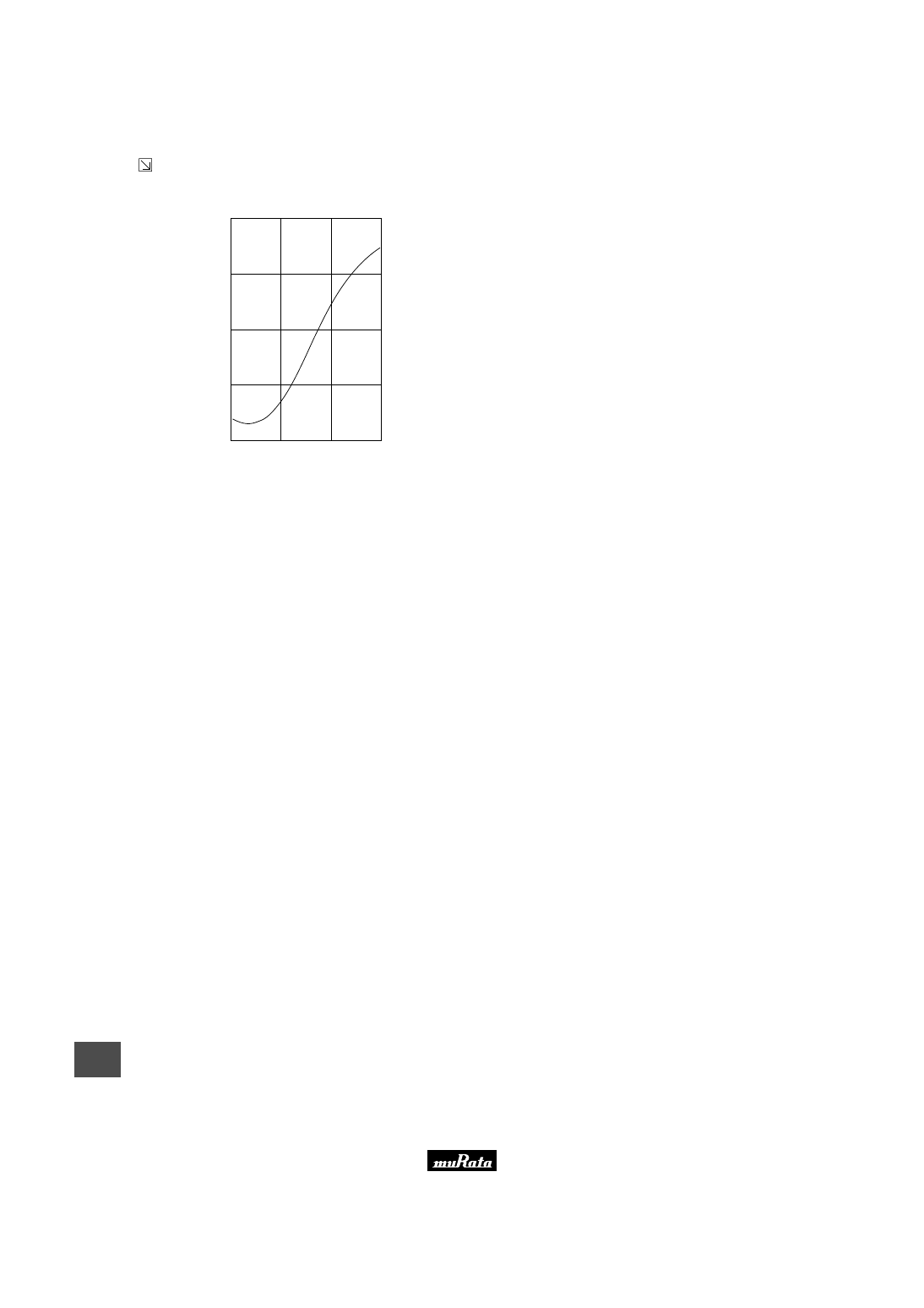
64
18
!
Note
• Please read rating and
!
CAUTION (for storage and operating, rating, soldering and mounting, handling) in this catalog to prevent smoking and/or burning, etc.
• This catalog has only typical specifications because there is no space for detailed specifications. Therefore, please approve our product specification or transact the approval sheet for product specification before ordering.
Continued from the preceding page.
■ S Curve Specification
CDBCB455KCAY54-R0
440
450
460
470
0.0
0.1
0.2
0.3
0.4
Frequency (kHz)
V
o
lt
(
V
)
Please read rating and
!
CAUTION (for storage and operating, rating, soldering and mounting, handling) in this PDF catalog to prevent smoking and/or burning, etc.
This catalog has only typical specifications. Therefore, you are requested to approve our product specification or to transact the approval sheet for product specificaion before ordering.
!
Note
P05E11.pdf 02.9.2

Ceramic Discriminators Notice
67
19
!
Note
• Please read rating and
!
CAUTION (for storage and operating, rating, soldering and mounting, handling) in this catalog to prevent smoking and/or burning, etc.
• This catalog has only typical specifications because there is no space for detailed specifications. Therefore, please approve our product specification or transact the approval sheet for product specification before ordering.
■ CDBCB Series Notice (Soldering and Mounting)
Filter is soldered one time within the following
temperature condition and then being placed in natural
condition for 24 hours.
1. Standard Reflow Soldering Condition
(1) Reflow
CFC alternatives(HCFC Series), Isopropyl Alcohol(IPA),
Water(Demineralized Water),Cleaning Water
Solution(Cleanthrough-750H,Pine Alha 100S),
Silicon(Technocare FRW)
2. Wash
(1) Cleaning Solvent
Immersion Wash
2 minutes max. in above solvent at +60
°
C max.
Shower or Rinse Wash
2 minutes max. in above solvent at +60
°
C max.
(2) Cleaning Conditions
When components are immersed in solvent, be sure to
maintain the temperature of components below the
temperature of solvent.
Please do not use ultrasonic cleaning.
Total washing time should be within 4minutes.
Please ensure the component is thoroughly evaluated
in your application circuit.
Please do not use chlorine, petroleum and alkali
cleaning solvent.
If you plan to use any other type of solvents, please
consult with Murata or MUrata representative prior to
using.
(3) Notice
Electrode is directly with the tip of soldering iron of +350
±
5
°
C for 3
±
1 seconds, and then being placed in natural
condition for 24hours.
(2) Soldering Iron
Peak
(235
°
C max.)
Heating
(200
°
C)
Gradual
Cooling
Pre-heating
(140-160
°
C)
100
200
240
T
e
m
p
e
ra
tu
re
(
°
C
)
30sec. min. 60sec.-120sec.
50sec. max. 120sec. min.
Continued on the following page.
Please read rating and
!
CAUTION (for storage and operating, rating, soldering and mounting, handling) in this PDF catalog to prevent smoking and/or burning, etc.
This catalog has only typical specifications. Therefore, you are requested to approve our product specification or to transact the approval sheet for product specificaion before ordering.
!
Note
P05E11.pdf 02.9.2

Ceramic Discriminators Notice
68
19
!
Note
• Please read rating and
!
CAUTION (for storage and operating, rating, soldering and mounting, handling) in this catalog to prevent smoking and/or burning, etc.
• This catalog has only typical specifications because there is no space for detailed specifications. Therefore, please approve our product specification or transact the approval sheet for product specification before ordering.
Continued from the preceding page.
■ CDSCA Series Notice (Soldering and Mounting)
1. Standard Reflow Soldering Condition
(1) Reflow
The component cannot be withstand washing.
2. Wash
Lead terminal is directly contacted with the tip of
soldering iron of +280
±
5
°
C for 3.0 seconds
±
0.5 seconds.
(2) Soldering Iron
5 sec
Gradual
Cooling
150
240
260
60
60
Time (sec.)
T
e
m
p
e
ra
tu
re
(
°
C
)
Please read rating and
!
CAUTION (for storage and operating, rating, soldering and mounting, handling) in this PDF catalog to prevent smoking and/or burning, etc.
This catalog has only typical specifications. Therefore, you are requested to approve our product specification or to transact the approval sheet for product specificaion before ordering.
!
Note
P05E11.pdf 02.9.2
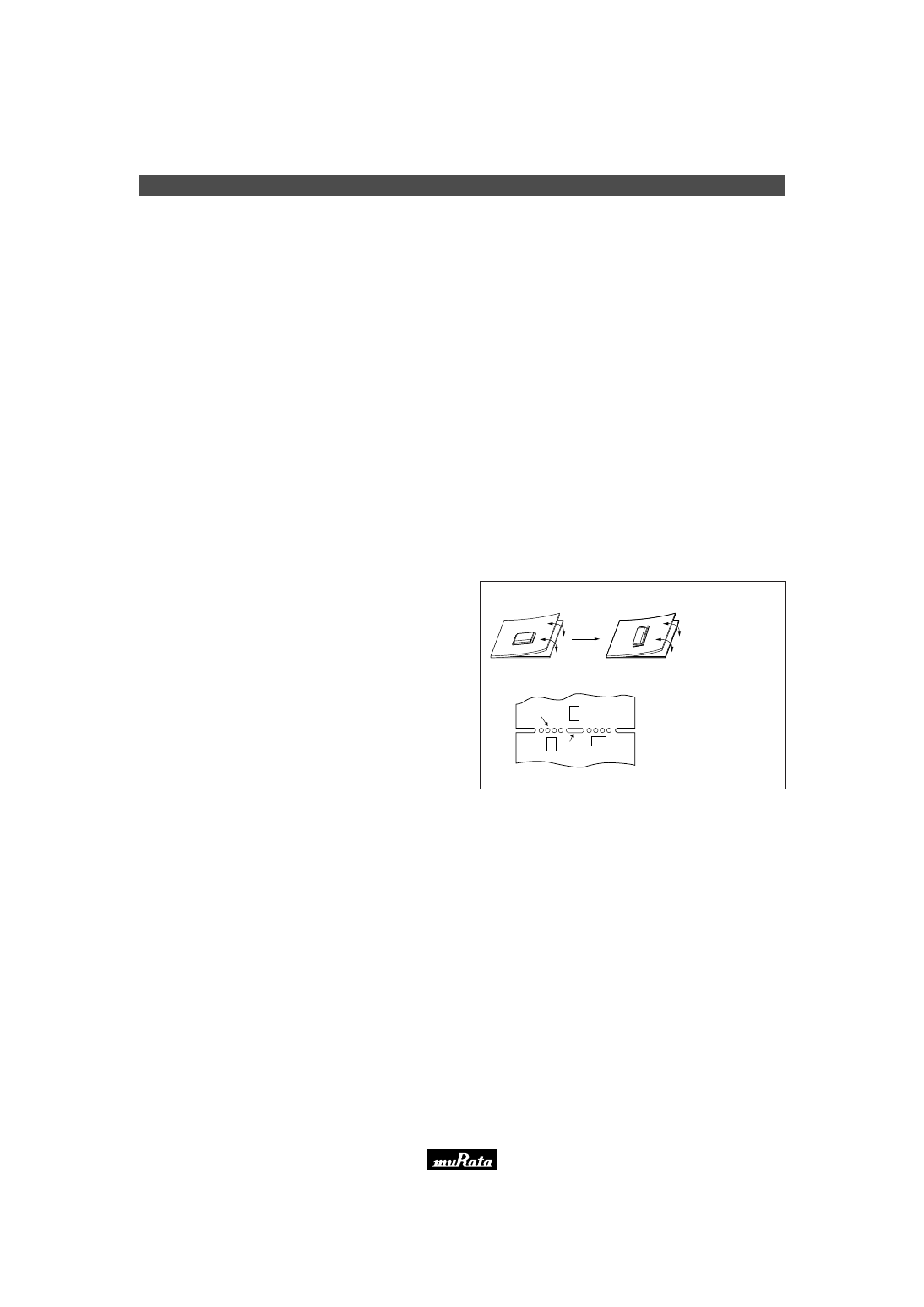
Ceramic Discriminators Notice
69
19
!
Note
• Please read rating and
!
CAUTION (for storage and operating, rating, soldering and mounting, handling) in this catalog to prevent smoking and/or burning, etc.
• This catalog has only typical specifications because there is no space for detailed specifications. Therefore, please approve our product specification or transact the approval sheet for product specification before ordering.
■ CDBCB Series Notice (Handling)
1. The component will be damaged when an excessive
stress is applied.
2. In the case that the component is cleaned, confirm
no reliability degradation is created.
3. In case of covering filter with over coat,
conditions such as material of resin, cure
temperature, and so on should be evaluated well.
4. Do not use strong acidity flux, more than 0.2wt%
chlorine content, in re-flow soldering.
5. The product, packed in the moisture-proof bag (dry
pack), is sensitive to moisture.
The following treatment is required before applying
re-flow soldering, to avoid package cracks or
reliability degradation caused by thermal stress.
When unpacked, store the component in an atmosphere
of below 25C. and below 65%R.H., and solder within
48 hours.
■ CDBLA/CDBLB Series Notice (Handling)
1. Do not use this product with bend. The component
may be damaged if excess mechanical stress is
applied to it mounted on the printed circuit board.
2. The component will be damaged when an excessive
stress is applied.
3. All kinds of re-flow soldering must not be applied
on the component.
4. Do not clean or wash the component as it is not
hermetically sealed.
5. Do not use strong acidity flux, more than 0.2wt%
chlorine content, in flow soldering.
6. In case of covering discriminator with over coat,
conditions such as material of resin, cure
emperature, and so on should be evaluated well.
■ CDSCA Series Notice (Handling)
1. The component mounted on the PCB may be damaged if
excess mechanical stress is applied.
2. Layout the components on the PCB to minimize the
stress imposed by the warp or flexure of the board.
3. After installing components, if solder is excessively
applied to the circuit board, mechanical stress will cause
destruction resistance characteristics to be lower. To
prevent this, be extremely careful in determining shape
and dimension before designing the circuit board diagram.
4. When the positioning claw or pick up nozzle are worn, the
excess load is applied to the components while
positioning or placing are performed. Careful checking
and maintenance are necessary to prevent unexpected
trouble.
5. When correcting component's position with a soldering
iron, the tip of the soldering iron should not directly touch
the chip component. Depending on the soldering
conditions, the effective area of terminations may be
reduced. The use of solder containing Ag should be
considerd to prevent the electrode erosion.
6. Do not clean or wash the component as it is not
hermetically sealed.
7. In case of overcoating the part, coating conditions such
as material, curing temperature, and so on must be
evaluated deeply.
8. Accurate test circuit values are required to measure
electrical characteristics.
It may be a cause of mis-correlation if there is any
deviation, especially stray capacitance, from the test
circuit in the specification.
[Component direction]
[Component layout close to board]
Put the
component
laterally to the
direction in
which stress
acts.
Susceptibility to
stress is in the order
of : A>C>B
B
A
C
Slit
Perforation
Please read rating and
!
CAUTION (for storage and operating, rating, soldering and mounting, handling) in this PDF catalog to prevent smoking and/or burning, etc.
This catalog has only typical specifications. Therefore, you are requested to approve our product specification or to transact the approval sheet for product specificaion before ordering.
!
Note
P05E11.pdf 02.9.2
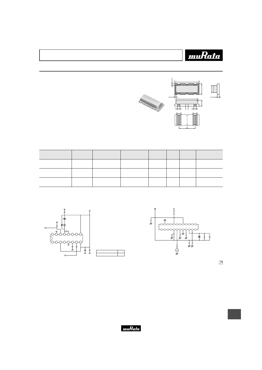
65
19
!
Note
• Please read rating and
!
CAUTION (for storage and operating, rating, soldering and mounting, handling) in this catalog to prevent smoking and/or burning, etc.
• This catalog has only typical specifications because there is no space for detailed specifications. Therefore, please approve our product specification or transact the approval sheet for product specification before ordering.
Ceramic Filters (CERAFILr)/Ceramic Discriminators for Communications Equipment
MHz Type Ceramic Discriminators
CDSCA10M7 series forms a resonator on a piezo electric
ceramic sabstrate. In combination with ICs, this type
obtains stable demoduration characteristics in wide
bandwidth.
■ Features
1. Compact and high reliability and recommended for
automotive applications.
2. Can be combined with various ICs. The IC is
determined by the last number in the part number.
3. Stable demoduration characteristics can be
obtained without adjustment.
4. Stable temperature characteristics.
5. Recommended for Pb free soldering.
4.1max
1
.2
m
a
x
4.5
±
0.1
0.2
±
0.2
2
.0
±
0
.1
0
.3
±
0
.2
0.4(ref.)
0.4(ref.)
1
.4
m
a
x
0.4
±
0.05
1.5
±
0.1
0.8
±
0.1
0.8
±
0.1
1.5
±
0.1
(in mm)
CDSCA Series
Part Number
Nominal Center
Frequency (fn)
(MHz)
Recovered
Audio 3dB BW
(kHz)
Recovered
Audio Output
(mV)
Distortion
(at fn)
(%)
IC
IC Maker
Type
CDSCA10M7GF072-R0
10.700
fn
±
150 min.
130 min.
2.0 max.
TA31161
TOSHIBA
SMD
CDSCA10M7GF107-R0
10.700
fn
±
80 min.
52 min.
3.0 max.
TA31272F
TOSHIBA
SMD
CDSCA10M7GF109-R0
10.700
fn
±
100 min.
170 min.
3.0 max.
TK14588V
TOKO
SMD
■ Test Circuit
CDSCA10M7GF072-R0
16
Vcc (3V)
9
10
11
12
13
14
15
1
8
7
6
5
4
3
2
IF-IN
AF-OUT
0.01
µ
33
µ
0.01
µ
R
10p
4.7
µ
X
0.01
µ
0.01
µ
0
.0
1
µ
+
TA31161 (TOSHIBA)
CDSCA10M7GF072-R0
Part Number (X)
R
820
Unit C : F
R :
Ω
CDSCA10M7GF107-R0
4
5
6
7
8
9
3
2
1
21
20 19 18 17 16 15 14 13
10 11 12
22
23
24
TA31272F
S.S.G.
X: CDSCA10M7GF107-B0
R: 1.2 [kohm]
C: open
X
R
C
0.01
µ
F
0.1
µ
F
0.01
µ
F
AF OUT
Vcc (5.0V)
0.1
µ
F
0.01
µ
F
1
0
0
0
p
F
0
.0
1
µ
F
0
.0
1
µ
F
Continued on the following page.
Please read rating and
!
CAUTION (for storage and operating, rating, soldering and mounting, handling) in this PDF catalog to prevent smoking and/or burning, etc.
This catalog has only typical specifications. Therefore, you are requested to approve our product specification or to transact the approval sheet for product specificaion before ordering.
!
Note
P05E11.pdf 02.9.2
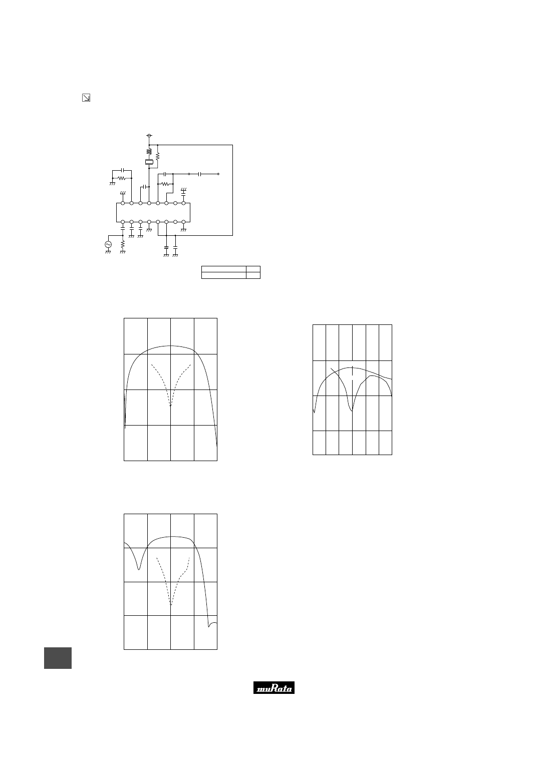
66
19
!
Note
• Please read rating and
!
CAUTION (for storage and operating, rating, soldering and mounting, handling) in this catalog to prevent smoking and/or burning, etc.
• This catalog has only typical specifications because there is no space for detailed specifications. Therefore, please approve our product specification or transact the approval sheet for product specification before ordering.
Continued from the preceding page.
■ Test Circuit
CDSCA10M7GF109-R0
8
7
6
5
4
3
2
1
9
10
11
12
13
14
15
16
0.01
µ
0.01
µ
Vcc (3V)
12k
51k
1000p
8p
+
S.S.G.
R
D.C. OUT
AF OUT
X
0
.0
1
µ
0
.0
1
µ
0
.0
1
µ
0
.0
1
µ
4
.7
µ
5
1
0
.0
1
µ
1
.2
µ
TK14588V (TOKO)
CDSCA10M7GF109-R0
Part Number (X)
R
820
Unit C
R
L
: F
:
Ω
: H
■ Frequency Characteristics
CDSCA10M7GF072-R0
A
F
O
u
tp
u
t
V
o
lt
a
g
e
(
m
V
)
T
.H
.D
.
(%
)
Frequency (MHz)
100
10
1000
100
10
1
1
0.1
10.3
10.5
10.7
10.9
11.1
CDSCA10M7GF107-R0
R
e
c
o
v
e
re
d
A
F
O
u
tp
u
t
V
o
lt
a
g
e
(m
V
)
D
is
to
rt
io
n
(
%
)
Frequency (MHz)
10.5
10.4
10.6
10.7
10.8
10.9
11.0
1
10
100
1000
0.1
1
10
100
AF Output
Distortion
Input Level
Mod. Freq.
Freq.Dev.
100dB
µ
1000Hz
±
40kHz
Input signal conditions
CDSCA10M7GF109-R0
A
F
O
u
tp
u
t
V
o
lt
a
g
e
(
m
V
)
T
.H
.D
.
(%
)
Frequency (MHz)
1000
100
10
1
100
10
1
0.1
10.3
10.5
10.7
10.9
11.1
Please read rating and
!
CAUTION (for storage and operating, rating, soldering and mounting, handling) in this PDF catalog to prevent smoking and/or burning, etc.
This catalog has only typical specifications. Therefore, you are requested to approve our product specification or to transact the approval sheet for product specificaion before ordering.
!
Note
P05E11.pdf 02.9.2
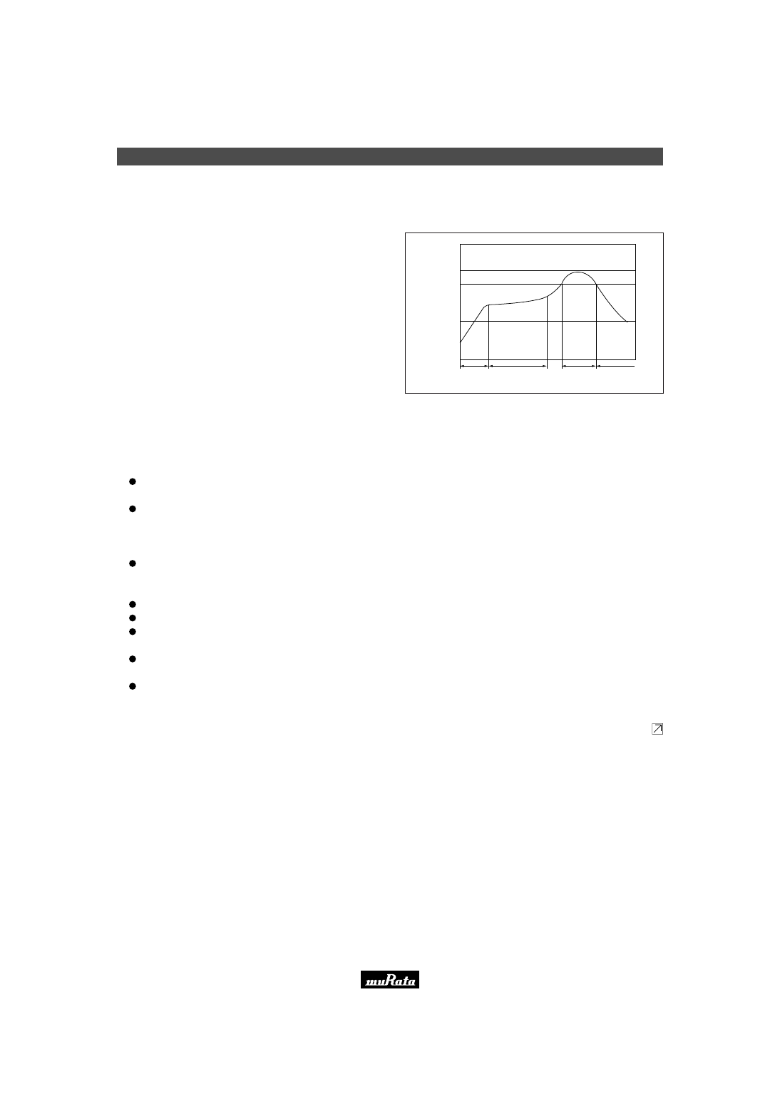
Ceramic Discriminators Notice
67
19
!
Note
• Please read rating and
!
CAUTION (for storage and operating, rating, soldering and mounting, handling) in this catalog to prevent smoking and/or burning, etc.
• This catalog has only typical specifications because there is no space for detailed specifications. Therefore, please approve our product specification or transact the approval sheet for product specification before ordering.
■ CDBCB Series Notice (Soldering and Mounting)
Filter is soldered one time within the following
temperature condition and then being placed in natural
condition for 24 hours.
1. Standard Reflow Soldering Condition
(1) Reflow
CFC alternatives(HCFC Series), Isopropyl Alcohol(IPA),
Water(Demineralized Water),Cleaning Water
Solution(Cleanthrough-750H,Pine Alha 100S),
Silicon(Technocare FRW)
2. Wash
(1) Cleaning Solvent
Immersion Wash
2 minutes max. in above solvent at +60
°
C max.
Shower or Rinse Wash
2 minutes max. in above solvent at +60
°
C max.
(2) Cleaning Conditions
When components are immersed in solvent, be sure to
maintain the temperature of components below the
temperature of solvent.
Please do not use ultrasonic cleaning.
Total washing time should be within 4minutes.
Please ensure the component is thoroughly evaluated
in your application circuit.
Please do not use chlorine, petroleum and alkali
cleaning solvent.
If you plan to use any other type of solvents, please
consult with Murata or MUrata representative prior to
using.
(3) Notice
Electrode is directly with the tip of soldering iron of +350
±
5
°
C for 3
±
1 seconds, and then being placed in natural
condition for 24hours.
(2) Soldering Iron
Peak
(235
°
C max.)
Heating
(200
°
C)
Gradual
Cooling
Pre-heating
(140-160
°
C)
100
200
240
T
e
m
p
e
ra
tu
re
(
°
C
)
30sec. min. 60sec.-120sec.
50sec. max. 120sec. min.
Continued on the following page.
Please read rating and
!
CAUTION (for storage and operating, rating, soldering and mounting, handling) in this PDF catalog to prevent smoking and/or burning, etc.
This catalog has only typical specifications. Therefore, you are requested to approve our product specification or to transact the approval sheet for product specificaion before ordering.
!
Note
P05E11.pdf 02.9.2
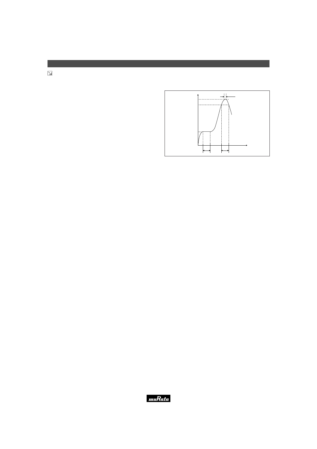
Ceramic Discriminators Notice
68
19
!
Note
• Please read rating and
!
CAUTION (for storage and operating, rating, soldering and mounting, handling) in this catalog to prevent smoking and/or burning, etc.
• This catalog has only typical specifications because there is no space for detailed specifications. Therefore, please approve our product specification or transact the approval sheet for product specification before ordering.
Continued from the preceding page.
■ CDSCA Series Notice (Soldering and Mounting)
1. Standard Reflow Soldering Condition
(1) Reflow
The component cannot be withstand washing.
2. Wash
Lead terminal is directly contacted with the tip of
soldering iron of +280
±
5
°
C for 3.0 seconds
±
0.5 seconds.
(2) Soldering Iron
5 sec
Gradual
Cooling
150
240
260
60
60
Time (sec.)
T
e
m
p
e
ra
tu
re
(
°
C
)
Please read rating and
!
CAUTION (for storage and operating, rating, soldering and mounting, handling) in this PDF catalog to prevent smoking and/or burning, etc.
This catalog has only typical specifications. Therefore, you are requested to approve our product specification or to transact the approval sheet for product specificaion before ordering.
!
Note
P05E11.pdf 02.9.2

Ceramic Discriminators Notice
69
19
!
Note
• Please read rating and
!
CAUTION (for storage and operating, rating, soldering and mounting, handling) in this catalog to prevent smoking and/or burning, etc.
• This catalog has only typical specifications because there is no space for detailed specifications. Therefore, please approve our product specification or transact the approval sheet for product specification before ordering.
■ CDBCB Series Notice (Handling)
1. The component will be damaged when an excessive
stress is applied.
2. In the case that the component is cleaned, confirm
no reliability degradation is created.
3. In case of covering filter with over coat,
conditions such as material of resin, cure
temperature, and so on should be evaluated well.
4. Do not use strong acidity flux, more than 0.2wt%
chlorine content, in re-flow soldering.
5. The product, packed in the moisture-proof bag (dry
pack), is sensitive to moisture.
The following treatment is required before applying
re-flow soldering, to avoid package cracks or
reliability degradation caused by thermal stress.
When unpacked, store the component in an atmosphere
of below 25C. and below 65%R.H., and solder within
48 hours.
■ CDBLA/CDBLB Series Notice (Handling)
1. Do not use this product with bend. The component
may be damaged if excess mechanical stress is
applied to it mounted on the printed circuit board.
2. The component will be damaged when an excessive
stress is applied.
3. All kinds of re-flow soldering must not be applied
on the component.
4. Do not clean or wash the component as it is not
hermetically sealed.
5. Do not use strong acidity flux, more than 0.2wt%
chlorine content, in flow soldering.
6. In case of covering discriminator with over coat,
conditions such as material of resin, cure
emperature, and so on should be evaluated well.
■ CDSCA Series Notice (Handling)
1. The component mounted on the PCB may be damaged if
excess mechanical stress is applied.
2. Layout the components on the PCB to minimize the
stress imposed by the warp or flexure of the board.
3. After installing components, if solder is excessively
applied to the circuit board, mechanical stress will cause
destruction resistance characteristics to be lower. To
prevent this, be extremely careful in determining shape
and dimension before designing the circuit board diagram.
4. When the positioning claw or pick up nozzle are worn, the
excess load is applied to the components while
positioning or placing are performed. Careful checking
and maintenance are necessary to prevent unexpected
trouble.
5. When correcting component's position with a soldering
iron, the tip of the soldering iron should not directly touch
the chip component. Depending on the soldering
conditions, the effective area of terminations may be
reduced. The use of solder containing Ag should be
considerd to prevent the electrode erosion.
6. Do not clean or wash the component as it is not
hermetically sealed.
7. In case of overcoating the part, coating conditions such
as material, curing temperature, and so on must be
evaluated deeply.
8. Accurate test circuit values are required to measure
electrical characteristics.
It may be a cause of mis-correlation if there is any
deviation, especially stray capacitance, from the test
circuit in the specification.
[Component direction]
[Component layout close to board]
Put the
component
laterally to the
direction in
which stress
acts.
Susceptibility to
stress is in the order
of : A>C>B
B
A
C
Slit
Perforation
Please read rating and
!
CAUTION (for storage and operating, rating, soldering and mounting, handling) in this PDF catalog to prevent smoking and/or burning, etc.
This catalog has only typical specifications. Therefore, you are requested to approve our product specification or to transact the approval sheet for product specificaion before ordering.
!
Note
P05E11.pdf 02.9.2
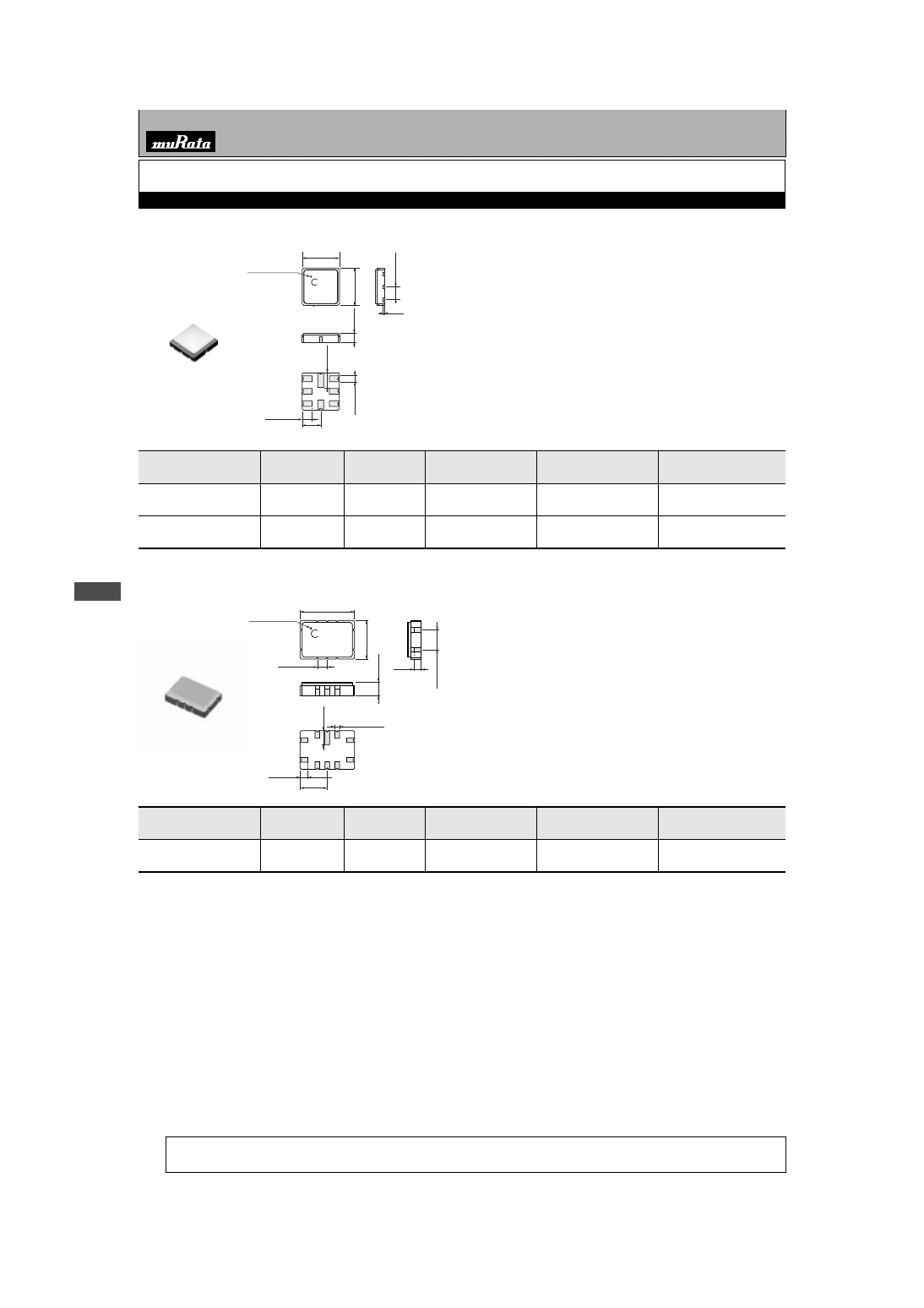
Filters for Communication Equipment
7
Filters for Communication Equipment
320
!
Note
• This catalog has only typical specifications because there is no space for detailed specifications. Therefore, please approve our product specifications or transact the approval sheet for product specifications
before ordering. Especially, please read rating and
!
CAUTION (for storage, operating, rating, soldering, mounting and handling) in them to prevent smoking and/or burning, etc.
• You are able to read a detailed specifications in the website (http://search.murata.co.jp/) before to require our product specifications or to transact the approval sheet for product specifications.
for IF
SAW Filters
o
AMPS/ADC
SAFCG130MCA0T00
(0.20)
1.15max.
1.50
±
0.13
1.9
±
0.2
8-0.6
±
0.08
7-1.00
±
0.13
3.8
±
0.2
3.8
±
0.2
Dot Marking(ø0.2)
(8)
(1)
(5)
(7)
(6)
(2)
(3)
(4)
4-1.27
±
0.13
M
Laser Printing
EIAJ Code
Marking :
∗
:
(in mm)
Pin
Input
Input (Ground)
Output
Output (Ground)
Ground
(8) :
(6) :
(4) :
(2) :
Others :
∗
Part Number
Center
Frequency
(MHz)
3dB Bandwidth
(kHz)
Insertion Loss
(dB)
Ripple (dB max.)
Input/Output
Impedance
SAFCG130MCA0T00
130.380
±
630 min.
5.5 max.
(at fo point)
-
310ohm//1.6
µ
H (Input)
310ohm//1.6
µ
H (Output)
SAFCT85M3JB0X05
85.380
±
12 min.
5.5 max.
(at min. loss point)
1.5
(fo
±
12kHz)
870ohm//-1.8pF (Input)
870ohm//-1.8pF (Output)
o
DECT
7.0
±
0.2
4-1.27
±
0.15
M
3.5
±
0.2
9-1.0
±
0.2
10-0.60
±
0.15
(0.90)
5.0
±
0.2
2-2.54
±
0.15
1.8 max.
1.8
±
0.2
Dot Marking(ø0.3)
Marking :
∗
:
Laser Printing
EIAJ Code
(in mm)
Input
Output
Ground
(9) :
(4) :
Others :
∗
(1)
(2)
(10)
(3)
(4)
(9)
(8)
(5)
(6)
(7)
Part Number
Center
Frequency
(MHz)
3dB Bandwidth
(kHz)
Insertion Loss
(dB)
Ripple (dB max.)
Input/Output
Impedance
SAFCT110MCA1T00
110.592
±
576 min.
4.5 max.
(at min. loss point)
-
300ohm//1.2
µ
H (Input)
300ohm//1.2
µ
H (Output)
04.10.20
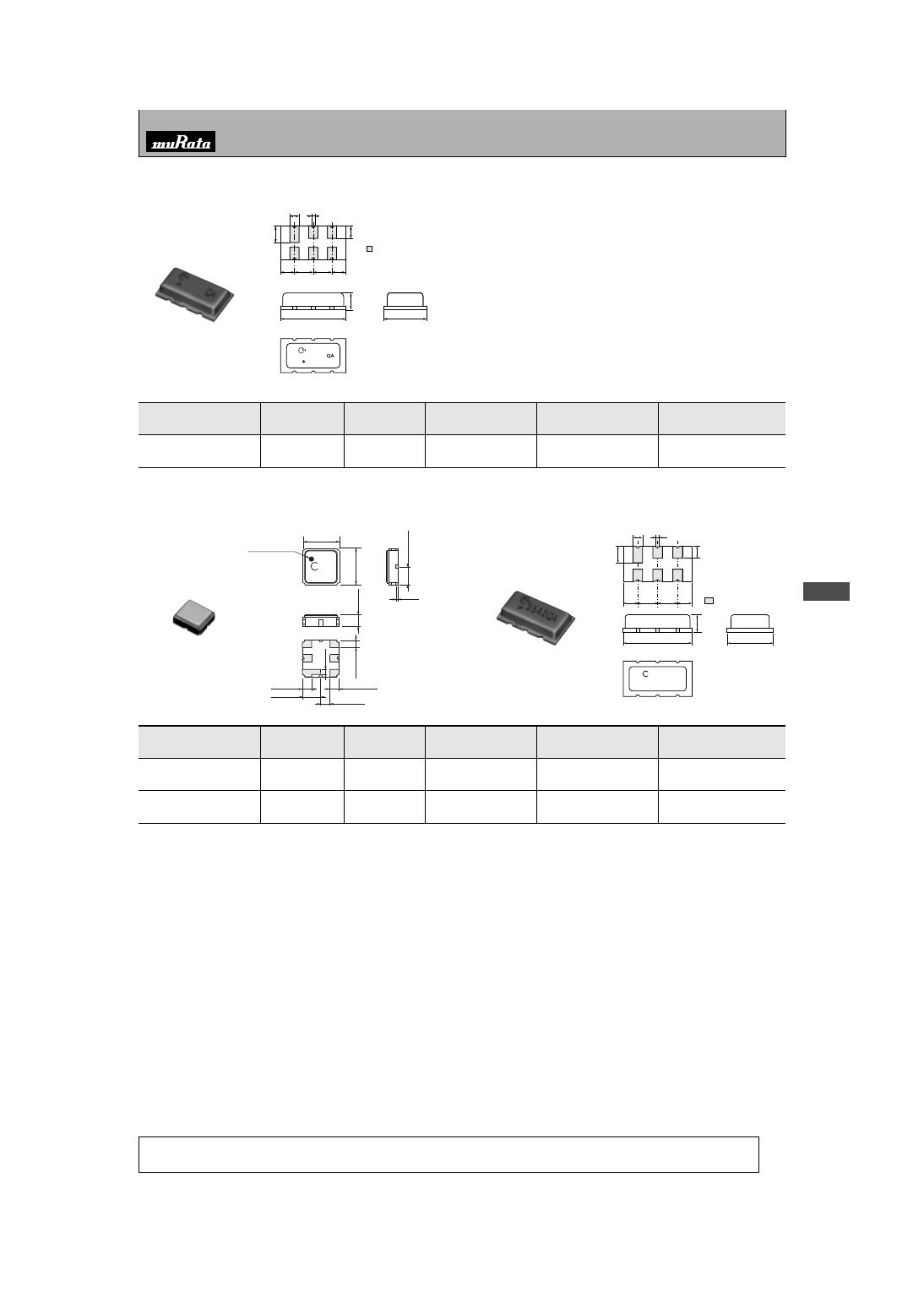
7
F
il
te
rs
f
o
r
C
o
m
m
u
n
ic
a
ti
o
n
E
q
u
ip
m
e
n
t
321
!
Note
• This catalog has only typical specifications because there is no space for detailed specifications. Therefore, please approve our product specifications or transact the approval sheet for product specifications
before ordering. Especially, please read rating and
!
CAUTION (for storage, operating, rating, soldering, mounting and handling) in them to prevent smoking and/or burning, etc.
• You are able to read a detailed specifications in the website (http://search.murata.co.jp/) before to require our product specifications or to transact the approval sheet for product specifications.
o
ETCS
(1) Ground
(2) Ground
(3) Output
(4) Output
(5) Ground
(6) Input
: Electrode
1.0
±
0.1
2.3
±
0.1
9.6
±
0.2
2.5
±
0.1
2.5
±
0.1
2.3
±
0.1
(1)
0.6
±
0.2
(2)
(3)
(6)
(6)
(5)
(4)
(1)
(2)
(3)
(5)
(4)
2
.5
5
±
0
.1
1
.5
±
0
.1
5.1
±
0.2
2
.0
m
a
x
.
(1)
(2)
(3)
(6)
(5)
(4)
(in mm)
Part Number
Center
Frequency
(MHz)
3dB Bandwidth
(MHz)
Insertion Loss
(dB)
Ripple (dB max.)
Input/Output
Impedance
SAFJA40M0WQAZ00R10
40.000
±
2.5 min.
21.5 max.
(at min. loss point)
-
-
o
GPS
SAFCC110MCA1T00
(1)
(2)
(3)
(4)
(5)
(6)
0.75
±
0.20
1.50
±
0.20
5-0.75
±
0.20
0.75
±
0.10
6
-0
.6
0
±
0
.1
5
3.0
±
0.2
3
.0
±
0
.2
0
.4
±
0
.1
M
(in mm)
Pin
1
.1
5
m
a
x
.
4
-1
.5
0
±
0
.1
5
(0.20)
Dot Marking(ø0.5)
Marking :
∗
:
Laser Printing
EIAJ Code
Input
Input
(or Ground)
Output
Output
(or Ground)
Ground
(3) :
(2) :
(6) :
(5) :
Others :
∗
SAFJA35M4WC0Z00R03
2.3
±
0.1
2.55
±
0.1
1.5
±
0.1
2.0 max.
: Electrode
1.0
±
0.1 0.6
±
0.2
2.3
±
0.1
(6)
(5)
(4)
(6)
(5)
(4)
(1)
(2)
(3)
(1)
(2)
(3)
2.5
±
0.1
2.5
±
0.1
9.6
±
0.2
35.42C
(1) Input or Ground
(2) Ground
(3) Output
(4) Output or Ground
(5) Ground
(6) Input
M
∗
5.1
±
0.2
(in mm)
Filters for Communication Equipment
Part Number
Center
Frequency
(MHz)
3dB Bandwidth
(MHz)
Insertion Loss
(dB)
Ripple (dB max.)
Input/Output
Impedance
SAFCC110MCA1T00
110.0
±
1.023 min.
3.7 max.
(at min. loss point)
0.6
480ohm//-1.6
µ
H (Input)
650ohm//-1.6
µ
H (Output)
SAFJA35M4WC0Z00R03
35.42
(fn)
1.90 min.
(1dB Bandwidth)
20.5 max.
(at fn)
1.6
(within 34.62 to 36.22MHz)
14.3k ohm//5.1pF (Input)
4.0k ohm//5.1pF (Output)
04.10.20
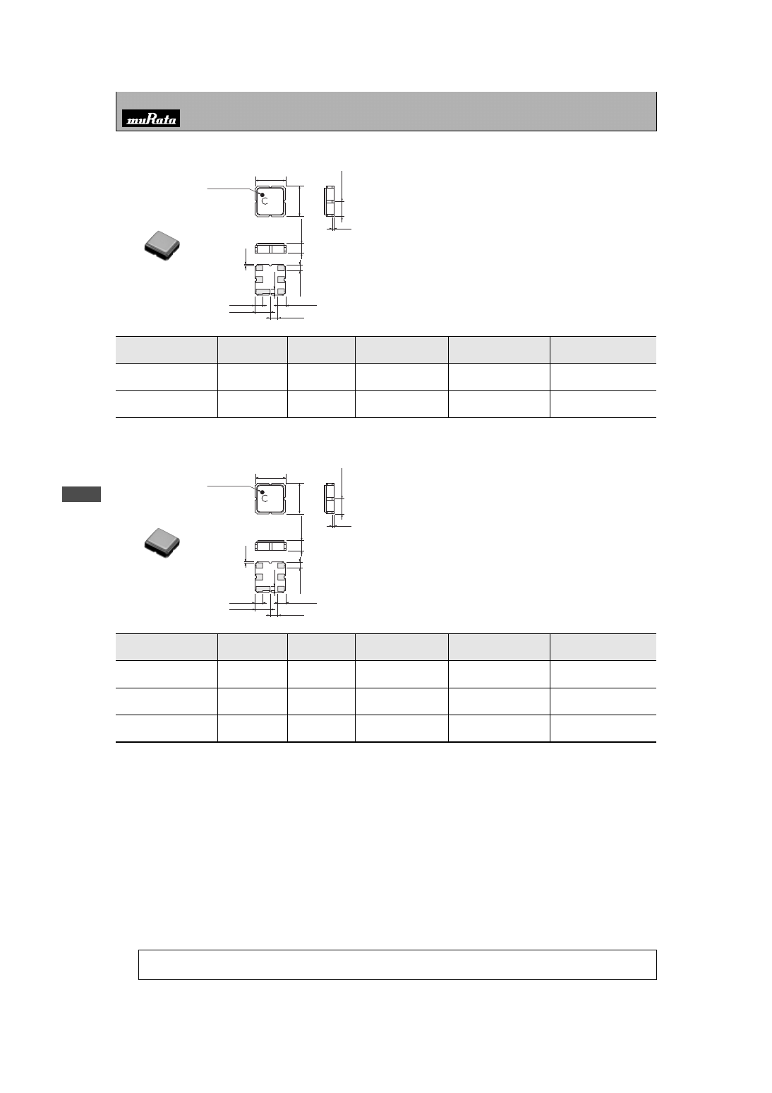
Filters for Communication Equipment
7
F
il
te
rs
f
o
r
C
o
m
m
u
n
ic
a
ti
o
n
E
q
u
ip
m
e
n
t
322
!
Note
• This catalog has only typical specifications because there is no space for detailed specifications. Therefore, please approve our product specifications or transact the approval sheet for product specifications
before ordering. Especially, please read rating and
!
CAUTION (for storage, operating, rating, soldering, mounting and handling) in them to prevent smoking and/or burning, etc.
• You are able to read a detailed specifications in the website (http://search.murata.co.jp/) before to require our product specifications or to transact the approval sheet for product specifications.
o
GSM
SAFCC225MRA0X00
(1)
(2)
(3)
(4)
(5)
(6)
0.75
±
0.20
1.50
±
0.20
5-0.75
±
0.20
0.75
±
0.10
6
-0
.6
0
±
0
.1
5
(0
.1
0
)
3.0
±
0.2
3
.0
±
0
.2
0
.4
±
0
.1
M
(in mm)
Pin
1
.1
5
m
a
x
.
4
-1
.5
0
±
0
.1
5
(0.20)
Dot Marking (ø0.5)
Marking :
∗
:
Laser Printing
EIAJ Code
Input
Output
Ground
(2) :
(5) :
Others :
∗
Part Number
Center
Frequency
(MHz)
3dB Bandwidth
(kHz)
Insertion Loss
(dB)
Ripple (dB max.)
Input/Output
Impedance
SAFCC225MRA0X00
225.000
±
80 min.
9.0 max.
(at min. loss point)
1.5
(fo
±
80kHz)
1100ohm//-0.42pF (Input)
900ohm//-0.30pF (Output)
SAFCC282MRA0X01
282.000
±
80 min.
9.0 max.
(at min. loss point)
1.5
(fo
±
80kHz)
1000ohm//-0.34pF (Input)
860ohm//-0.34pF (Output)
o
PHS
SAFCC243MRB9X00
(1)
(2)
(3)
(4)
(5)
(6)
0.75
±
0.20
1.50
±
0.20
5-0.75
±
0.20
0.75
±
0.10
6
-0
.6
0
±
0
.1
5
(0
.1
0
)
3.0
±
0.2
3
.0
±
0
.2
0
.4
±
0
.1
M
(in mm)
Pin
1
.1
5
m
a
x
.
4
-1
.5
0
±
0
.1
5
(0.20)
Dot Marking (ø0.5)
Marking :
∗
:
Laser Printing
EIAJ Code
Input
Output
Ground
(2) :
(5) :
Others :
∗
Part Number
Center
Frequency
(MHz)
3dB Bandwidth
(kHz)
Insertion Loss
(dB)
Ripple (dB max.)
Input/Output
Impedance
SAFCC243MRB9X00
243.950
±
130 min.
4.5 max.
(at min. loss point)
1.0
(fo
±
100kHz)
760ohm//-1.0pF (Input)
760ohm//-0.8pF (Output)
SAFCC265MRB5X01
265.550
±
130 min.
4.5 max.
(at fo point)
1.0
(fo
±
100kHz)
740ohm//-1.0pF (Input)
820ohm//-0.9pF (Output)
SAFDA243MRD9X00
243.950
±
130 min.
4.5 max.
(at fo point)
1.0
(fo
±
100kHz)
760ohm//-1.0pF (Input)
760ohm//-0.8pF (Output)
04.10.20
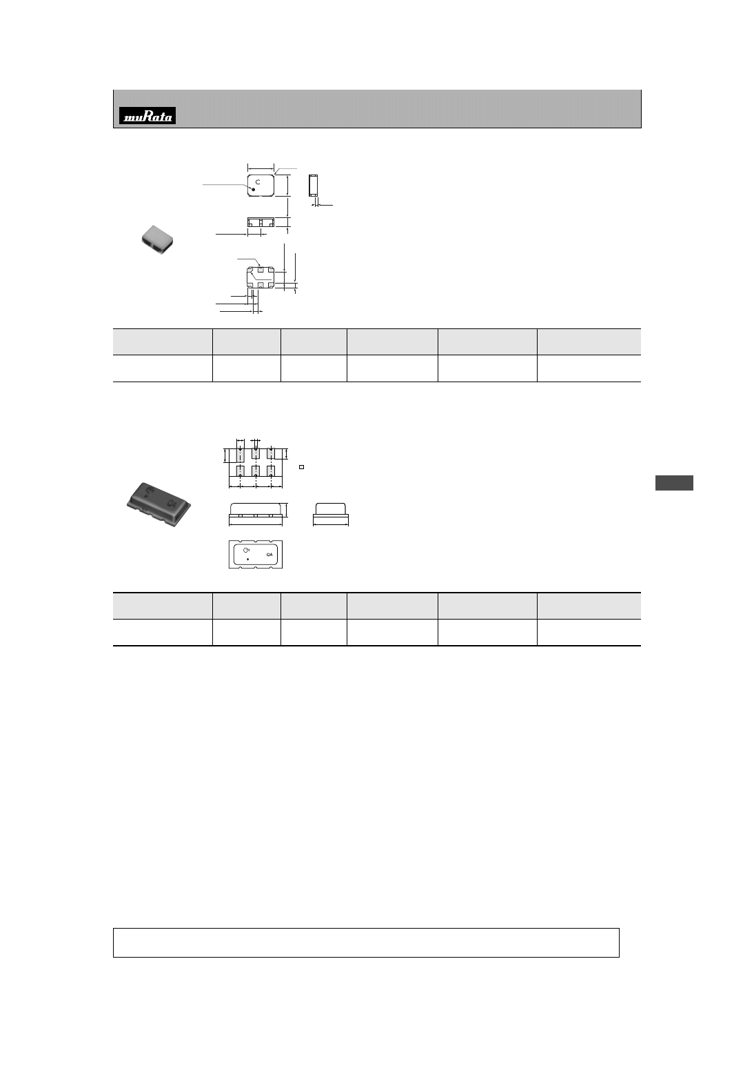
7
F
il
te
rs
f
o
r
C
o
m
m
u
n
ic
a
ti
o
n
E
q
u
ip
m
e
n
t
323
!
Note
• This catalog has only typical specifications because there is no space for detailed specifications. Therefore, please approve our product specifications or transact the approval sheet for product specifications
before ordering. Especially, please read rating and
!
CAUTION (for storage, operating, rating, soldering, mounting and handling) in them to prevent smoking and/or burning, etc.
• You are able to read a detailed specifications in the website (http://search.murata.co.jp/) before to require our product specifications or to transact the approval sheet for product specifications.
o
W-CDMA
(in mm)
Pin
Input
Input
(or Ground)
Output
Output
(or Ground)
Ground
(1) :
(3) :
(4) :
(6) :
Others :
Dot Marking(ø0.4)
R2-0.12
1
.0
m
a
x
.
(0.25)
(3)
(2)
(1)
(4)
(5)
(6)
(0.40)
(C0.3)
M
2.5
±
0.2
4-1.25
±
0.15
6-0.50
±
0.15
4-0.50
±
0.10
2
-0
.7
4
±
0
.1
0
6
-0
.6
3
±
0
.1
5
2
.0
±
0
.2
Marking :
∗
:
Laser Printing
EIAJ Code
∗
R4-0.15
Part Number
Center
Frequency
(MHz)
3dB Bandwidth
(MHz)
Insertion Loss
(dB)
Ripple (dB max.)
Input/Output
Impedance
SAFSD570MCM0T00
570
±
2.5 min.
3.5 max.
(at fo point)
0.8
(fo
±
1.92MHz)
310ohm//120nH (Input)
310ohm//120nH (Output)
o
Wireless LAN
(1) Ground
(2) Ground
(3) Output
(4) Output
(5) Ground
(6) Input
: Electrode
1.0
±
0.1
2.3
±
0.1
9.6
±
0.2
2.5
±
0.1
2.5
±
0.1
2.3
±
0.1
(1)
0.6
±
0.2
(2)
(3)
(6)
(6)
(5)
(4)
(1)
(2)
(3)
(5)
(4)
2
.5
5
±
0
.1
1
.5
±
0
.1
5.1
±
0.2
2
.0
m
a
x
.
(1)
(2)
(3)
(6)
(5)
(4)
(in mm)
Part Number
Center
Frequency
(MHz)
3dB Bandwidth
(MHz)
Insertion Loss
(dB)
Ripple (dB max.)
Input/Output
Impedance
SAFJA43M0WC0Z00R03
43.00
±
0.1MHz
(fo)
1.25 min.
21.0 max.
(at fo point)
-
-
Filters for Communication Equipment
04.10.20
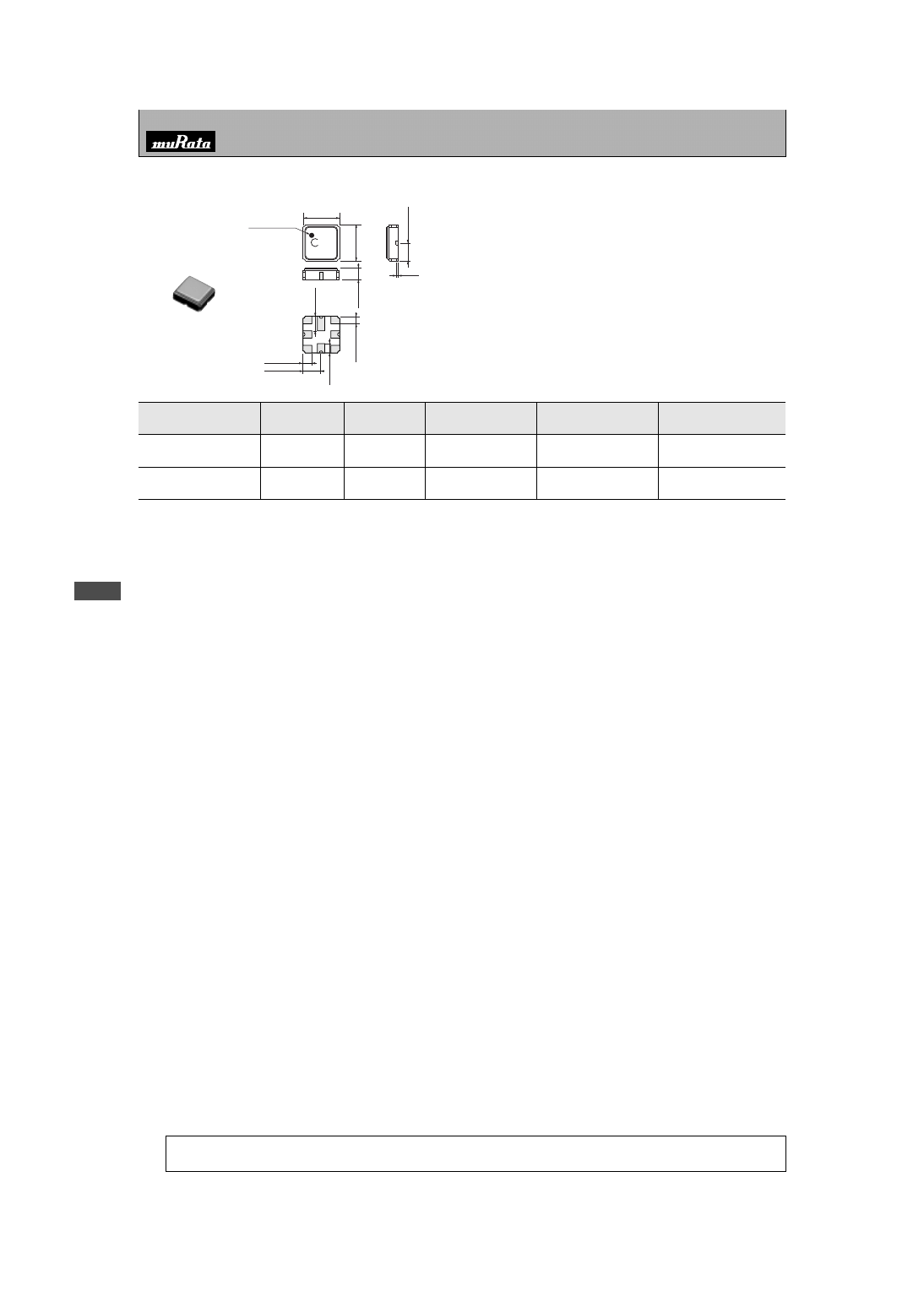
Filters for Communication Equipment
7
F
il
te
rs
f
o
r
C
o
m
m
u
n
ic
a
ti
o
n
E
q
u
ip
m
e
n
t
324
!
Note
• This catalog has only typical specifications because there is no space for detailed specifications. Therefore, please approve our product specifications or transact the approval sheet for product specifications
before ordering. Especially, please read rating and
!
CAUTION (for storage, operating, rating, soldering, mounting and handling) in them to prevent smoking and/or burning, etc.
• You are able to read a detailed specifications in the website (http://search.murata.co.jp/) before to require our product specifications or to transact the approval sheet for product specifications.
Part Number
Center
Frequency
(MHz)
3dB Bandwidth
(MHz)
Insertion Loss
(dB)
Ripple (dB max.)
Input/Output
Impedance
SAFCD450MCL0N00
450
±
8.2 min.
4.5 max.
(at min. loss point)
1.5
(fo
±
8.2MHz)
200ohm//150nH (Input)
200ohm//150nH (Output)
SAFCD570MCL0N00
570
±
8.5 min.
(2dB Bandwidth)
7.0 max.
(fo
±
8.5MHz)
2.0
(fo
±
8.5MHz)
200ohm//100nH (Input)
200ohm//100nH (Output)
o
5G W-LAN
SAFCD450MCL0N00
(5)
(4)
(6)
(7)
(8)
6-0.75
±
0.20
4-1.50
±
0.20
8
-0
.6
0
±
0
.1
5
3.0
±
0.2
3
.0
±
0
.2
M
1
.1
5
m
a
x
.
4
-1
.5
0
±
0
.1
5
(0.20)
0
.7
5
±
0
.2
0
Dot Marking(ø0.5)
Marking :
∗
:
Laser Printing
EIAJ Code
(in mm)
Pin
Input
Input (Ground)
Output
Output (Ground)
Ground
(3) :
(1) :
(7) :
(5) :
Others :
∗
(1)
(2)
(3)
1
.2
0
±
0
.2
0
04.10.20
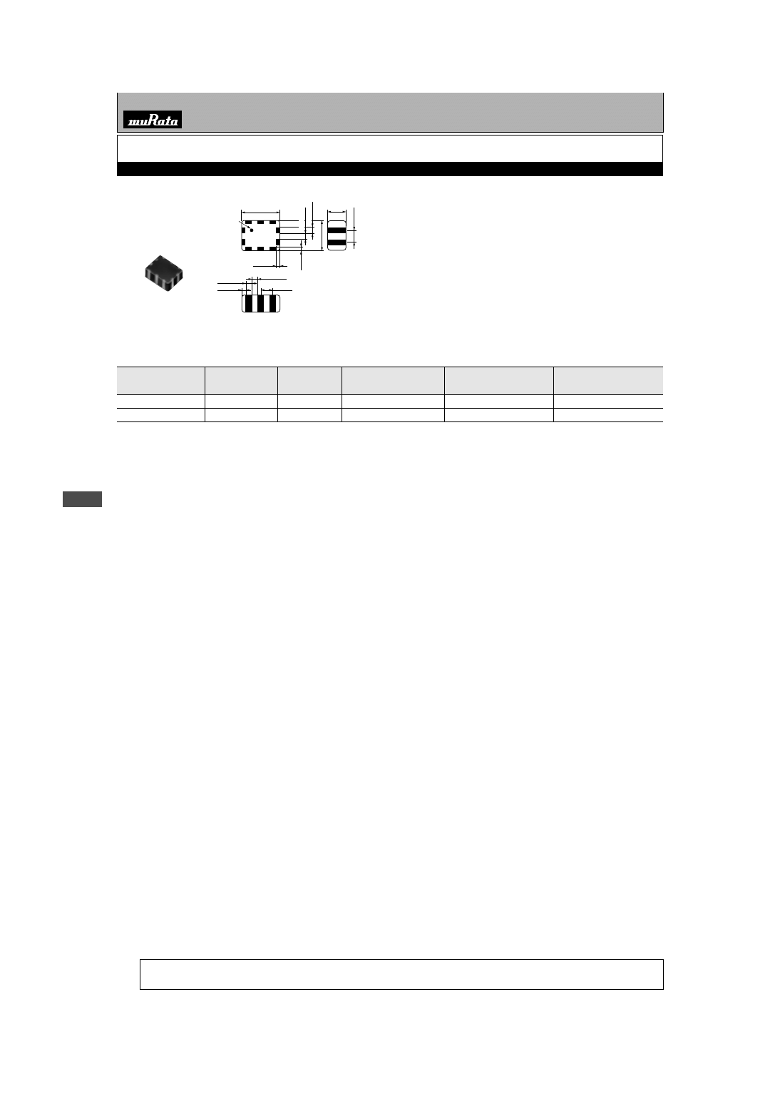
Filters for Communication Equipment
7
Filters for Communication Equipment
324
!
Note
• This catalog has only typical specifications because there is no space for detailed specifications. Therefore, please approve our product specifications or transact the approval sheet for product specifications
before ordering. Especially, please read rating and
!
CAUTION (for storage, operating, rating, soldering, mounting and handling) in them to prevent smoking and/or burning, etc.
• You are able to read a detailed specifications in the website (http://search.murata.co.jp/) before to require our product specifications or to transact the approval sheet for product specifications.
for IF
Chip LC Filters (Balance-balance Type)
LFB32130MSH3A569
∗
Terminal of "NC1" should be fixed to the no connected pattern.
Terminal of "NC2" should not be fixed to any pattern.
(in mm)
All the technical data and Information contained herein are
subject to change without prior notice.
(1)(3)
:
Balance IN
(2)(7)
:
NC1
(4)(5)(9)(10) :
NC2
(6)(8)
:
Balance OUT
1.5
±
0.1
0.8
±
0.1
0.40
±
0.15
0.4
±
0.2
0.60
±
0.15
1.0
±
0.1
3.2
±
0.2
(4)
(5)
(1) (2) (3)
(8) (7) (6)
2.5
±
0.2
0.3
±
0.2
0.3
±
0.2
(10)
(9)
Directional
Input Mark
0.40
±
0.15
0.40
±
0.15
Part Number
Nominal Center
Frequency (fo)
(MHz)
Bandwidth (BW)
(MHz)
Insertion Loss in BW
(dB)
Input Balance Impedance
(Differential) (Nom.)
(ohm)
Output Balance Impedance
(Differential) (Nom.)
(ohm)
LFB32130MSH3A569
130.38
fo
±
0.7
5.0 max. (at 25
°
C)
1000
250
LFB32166MSH2A570
166.85
fo
±
0.65
5.0 max. (at 25
°
C)
300
300
04.10.20
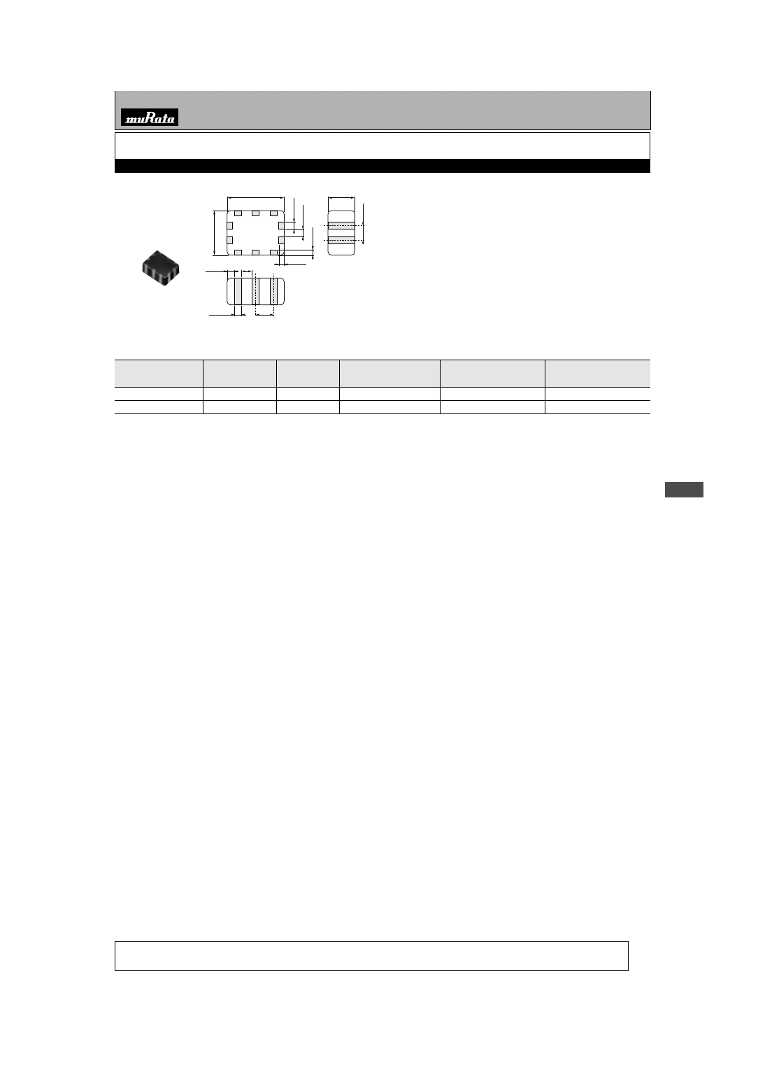
7
Filters for Communication Equipment
325
!
Note
• This catalog has only typical specifications because there is no space for detailed specifications. Therefore, please approve our product specifications or transact the approval sheet for product specifications
before ordering. Especially, please read rating and
!
CAUTION (for storage, operating, rating, soldering, mounting and handling) in them to prevent smoking and/or burning, etc.
• You are able to read a detailed specifications in the website (http://search.murata.co.jp/) before to require our product specifications or to transact the approval sheet for product specifications.
for IF
Chip LC Filters (Balance-unbalance Type)
LFB32130MSQ1A552
(in mm)
∗
Terminal of "NC1" should be fixed to the no connected pattern.
Terminal of "NC2" should not be fixed to any pattern.
All the technical data and Information contained herein are subject
to change without prior notice.
(1)
(2)
(3)
(8)
(10)
(9)
(4)
(5)
(7)
(6)
3.2
±
0.2
0.6
±
0.15
0.4
±
0.2
0.4
±
0.15
1.0
±
0.1
1.5
±
0.1
2.5
±
0.2
0.4
±
0.15
0.4
±
0.15
0.3
±
0.2
0.3
±
0.2
0.8
±
0.1
(1)(3) : Balance IN
(2)(7) : GND
(4)(5)(9)(10) : NC2
(6) : Unbalance OUT
(8) : NC1 (Biasing terminal)
Part Number
Nominal Center
Frequency (fo)
(MHz)
Bandwidth (BW)
(MHz)
Insertion Loss in BW
(dB)
Balance Impedance
(Differential) (Nom.)
(ohm)
Unbalance Impedance
(Nom.)
(ohm)
LFB32130MSQ1A552
130.38
fo
±
0.65
5.5 max. (at 25
°
C)
1000
50
LFB32166MSQ1A527
166.85
fo
±
0.7
4.0 max. (at 25
°
C)
200
50
Filters for Communication Equipment
04.10.20
Wyszukiwarka
Podobne podstrony:
NFM21P NFM39 Murata
BLM21B Murata
murata filtry dyskryminatory
BLM31P Murata
BLM41P Murata
dss306 DS306 EMI leaded filter Murata
BLM21P Murata
BLM18P Murata
NFM41P Murata
NFM3DC Murata
BLM18B Murata id 90170 Nieznany (2)
BNX022 EMI Murata
BLM21A Murata
muratafilter 147
BLM18A Murata
BLM31A Murata
BLM21B Murata
więcej podobnych podstron