1/11
September 2002
■
MEDIUM SPEED OPERATION :
8 MHz (Typ.) at 10V
■
SYNCHRONOUS INTERNAL CARRY
PROPAGATION
■
RESET AND PRESET CAPABILITY
■
STANDARDIZED SYMMETRICAL OUTPUT
CHARACTERISTICS
■
QUIESCENT CURRENT SPECIF. UP TO 20V
■
5V, 10V AND 15V PARAMETRIC RATINGS
■
INPUT LEAKAGE CURRENT
I
I
= 100nA (MAX) AT V
DD
= 18V T
A
= 25
°
C
■
100% TESTED FOR QUIESCENT CURRENT
■
MEETS ALL REQUIREMENTS OF JEDEC
JESD13B ”STANDARD SPECIFICATIONS
FOR DESCRIPTION OF B SERIES CMOS
DEVICES”
DESCRIPTION
HCF4516B is a monolithic integrated circuit
fabricated
in
Metal
Oxide
Semiconductor
technology available in DIP package.
It is a PRESETTABLE BINARY UP/DOWN
COUNTER,
consists
of
four
synchronously
clocked D-type flip-flops (with a gating structure to
provide T-type flip-flop capability) connected as a
counter. This counter can be cleared by a high
level on the RESET line, and can be preset to any
binary number present on the jam inputs by a high
level on the PRESET ENABLE line. Synchronous
cascading is accomplished by connecting all clock
inputs in parallel and connecting the CARRY OUT
of a less significant stage to the CARRY IN of a
more
significant
stage.
HCF4516B
can
be
cascaded in the ripple mode by connecting all
clock inputs in parallel and connecting the CARRY
OUT to the clock of the next stage. If the UP/
DOWN input changes during a terminal count, the
CARRY OUT must be gated with the clock, and
the UP/DOWN input must change while the clock
is high. This method provides a clean clock signal
to the subsequent counting stage.
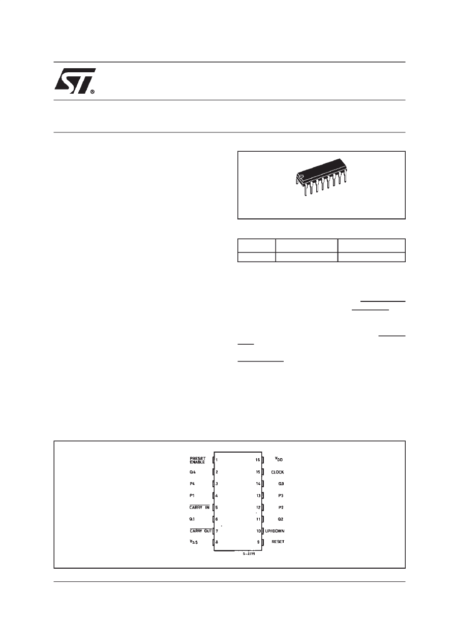
HCF4516B
PRESETTABLE BINARY UP/DOWN COUNTER
PIN CONNECTION
ORDER CODES
PACKAGE
TUBE
T & R
DIP
HCF4516BEY
DIP
HCF4516B
2/11
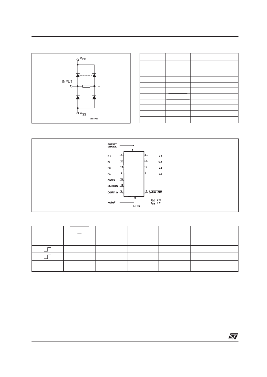
IINPUT EQUIVALENT CIRCUIT
PIN DESCRIPTION
FUNCTIONAL DIAGRAM
TRUTH TABLE
X : Don’t Care
PIN No
SYMBOL
NAME AND FUNCTION
1
PRESET
ENABLE
Preset Enable Input
4, 12, 13, 3
P1 to P4
Inputs
6, 11, 14, 2
Q1 to Q4
Outputs
15
CLOCK
Clock Input
10
UP/DOWN
Up/Down Control Input
5
CARRY-IN
Carry Input
7
CARRY-OUT Carry Output
9
RESET
Reset Input
8
V
SS
Negative Supply Voltage
16
V
DD
Positive Supply Voltage
CL
CARRY-IN
CI
UP/DOWN
PRESET
ENABLE
RESET
ACTION
X
H
X
L
L
NO COUNT
L
H
L
L
COUNT UP
L
L
L
L
COUNT DOWN
X
X
X
H
L
PRESET
X
X
X
X
H
RESET
HCF4516B
3/11
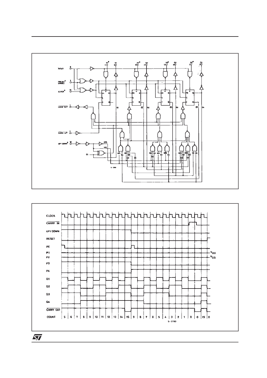
LOGIC DIAGRAM
TIMING CHART
HCF4516B
4/11
ABSOLUTE MAXIMUM RATINGS
Absolute Maximum Ratings are those values beyond which damage to the device may occur. Functional operation under these conditions is
not implied.
All voltage values are referred to V
SS
pin voltage.
RECOMMENDED OPERATING CONDITIONS
Symbol
Parameter
Value
Unit
V
DD
Supply Voltage
-0.5 to +22
V
V
I
DC Input Voltage
-0.5 to V
DD
+ 0.5
V
I
I
DC Input Current
±
10
mA
P
D
Power Dissipation per Package
200
mW
Power Dissipation per Output Transistor
100
mW
T
op
Operating Temperature
-55 to +125
°
C
T
stg
Storage Temperature
-65 to +150
°
C
Symbol
Parameter
Value
Unit
V
DD
Supply Voltage
3 to 20
V
V
I
Input Voltage
0 to V
DD
V
T
op
Operating Temperature
-55 to 125
°
C
HCF4516B
5/11
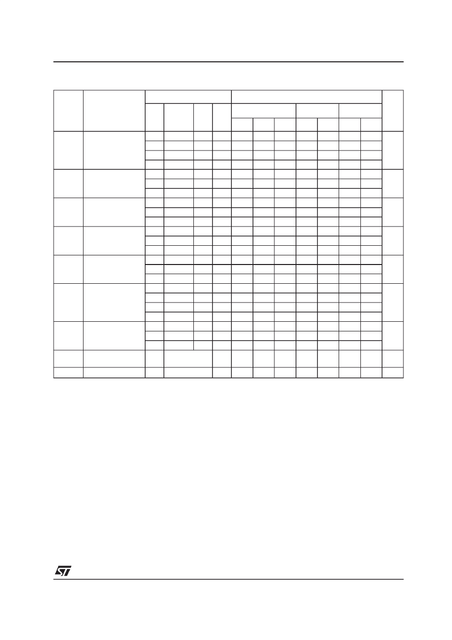
DC SPECIFICATIONS
The Noise Margin for both ”1” and ”0” level is: 1V min. with V
DD
=5V, 2V min. with V
DD
=10V, 2.5V min. with V
DD
=15V
Symbol
Parameter
Test Condition
Value
Unit
V
I
(V)
V
O
(V)
|I
O
|
(
µ
A)
V
DD
(V)
T
A
= 25
°
C
-40 to 85
°
C
-55 to 125
°
C
Min.
Typ.
Max.
Min.
Max.
Min.
Max.
I
L
Quiescent Current
0/5
5
0.04
5
150
150
µ
A
0/10
10
0.04
10
300
300
0/15
15
0.04
20
600
600
0/20
20
0.08
100
3000
3000
V
OH
High Level Output
Voltage
0/5
<1
5
4.95
4.95
4.95
V
0/10
<1
10
9.95
9.95
9.95
0/15
<1
15
14.95
14.95
14.95
V
OL
Low Level Output
Voltage
5/0
<1
5
0.05
0.05
0.05
V
10/0
<1
10
0.05
0.05
0.05
15/0
<1
15
0.05
0.05
0.05
V
IH
High Level Input
Voltage
0.5/4.5
<1
5
3.5
3.5
3.5
V
1/9
<1
10
7
7
7
1.5/13.5
<1
15
11
11
11
V
IL
Low Level Input
Voltage
4.5/0.5
<1
5
1.5
1.5
1.5
V
9/1
<1
10
3
3
3
13.5/1.5
<1
15
4
4
4
I
OH
Output Drive
Current
0/5
2.5
<1
5
-1.36
-3.2
-1.1
-1.1
mA
0/5
4.6
<1
5
-0.44
-1
-0.36
-0.36
0/10
9.5
<1
10
-1.1
-2.6
-0.9
-0.9
0/15
13.5
<1
15
-3.0
-6.8
-2.4
-2.4
I
OL
Output Sink
Current
0/5
0.4
<1
5
0.44
1
0.36
0.36
mA
0/10
0.5
<1
10
1.1
2.6
0.9
0.9
0/15
1.5
<1
15
3.0
6.8
2.4
2.4
I
I
Input Leakage
Current
0/18
Any Input
18
±
10
-5
±
0.1
±
1
±
1
µ
A
C
I
Input Capacitance
Any Input
5
7.5
pF
HCF4516B
6/11
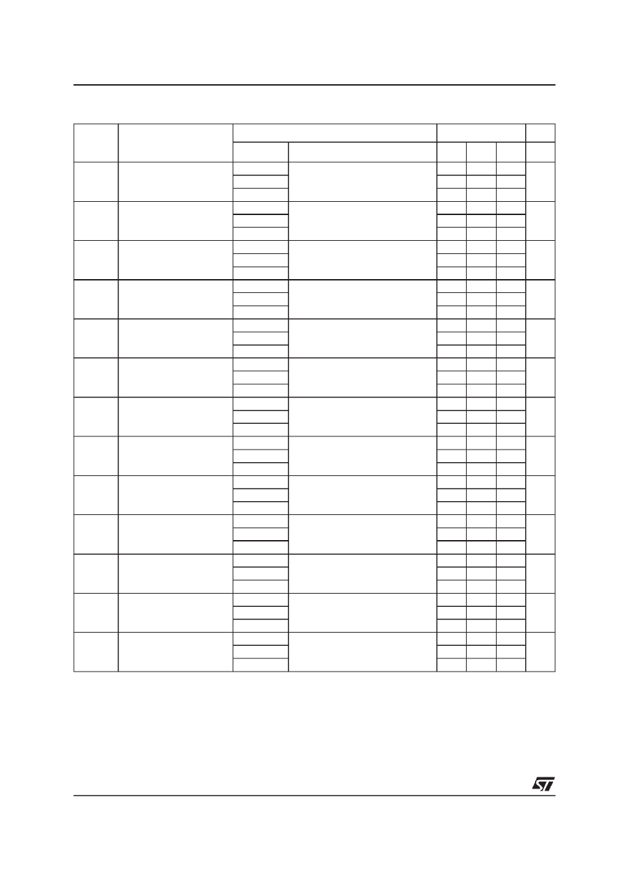
DYNAMIC ELECTRICAL CHARACTERISTICS (T
amb
= 25
°
C, C
L
= 50pF, R
L
= 200K
Ω
, t
r
= t
f
= 20 ns)
(*) Typical temperature coefficient for all V
DD
value is 0.3 %/
°
C.
(1) Time required after the falling edge of the reset or preset enable inputs before the rising edge of the clock will trigger the counter (similar
to setup time)
(2) If more than unit is cascaded in the parallel clocked application, trCL should be made less than or equal to the sum of the fixed propagation
delay at 15pF and the transition time of the carry output driving stage for the estimated capacitive load.
Symbol
Parameter
Test Condition
Value (*)
Unit
V
DD
(V)
Min.
Typ.
Max.
t
PHL
t
PLH
Propagation Delay Time
Clock to Q Output
5
200
400
ns
10
100
200
15
75
150
t
PHL
t
PLH
Propagation Delay Time
Preset or Reset to Q
Output
5
210
420
ns
10
105
210
15
80
160
t
PHL
t
PLH
Propagation Delay Time
Clock to Carry Out
5
240
480
ns
10
120
240
15
90
180
t
PHL
t
PLH
Propagation Delay Time
Carry in to Carry Out
5
125
250
ns
10
60
120
15
50
100
t
PHL
t
PLH
Propagation Delay Time
Preset or Reset to Carry
Out
5
320
640
ns
10
160
320
15
125
250
t
THL
t
TLH
Transition Time
5
100
200
ns
10
50
100
15
40
80
f
MAX
Maximum Clock
Frequency
5
2
4
MHz
10
4
8
15
5.5
11
t
W
Clock Pulse Width
5
150
ns
10
75
15
60
t
REM
(1)
Preset Enable or Reset
Removal Time
5
150
ns
10
80
15
60
t
r
, t
f
(2)
Clock Rise or Fall Time
5
15
µ
s
10
5
15
5
t
setup
Carry in Setup Time
5
130
ns
10
60
15
45
t
setup
Up/Down Setup Time
5
360
ns
10
160
15
110
t
W
Preset Enable or Reset
Pulse Width
5
220
ns
10
100
15
75
HCF4516B
7/11
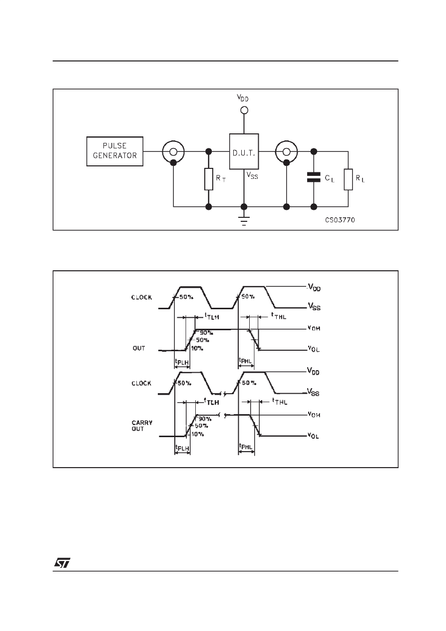
TEST CIRCUIT
C
L
= 50pF or equivalent (includes jig and probe capacitance)
R
L
= 200K
Ω
R
T
= Z
OUT
of pulse generator (typically 50
Ω
)
WAVEFORM 1 : PROPAGATION DELAY TIMES (f=1MHz; 50% duty cycle)
HCF4516B
8/11
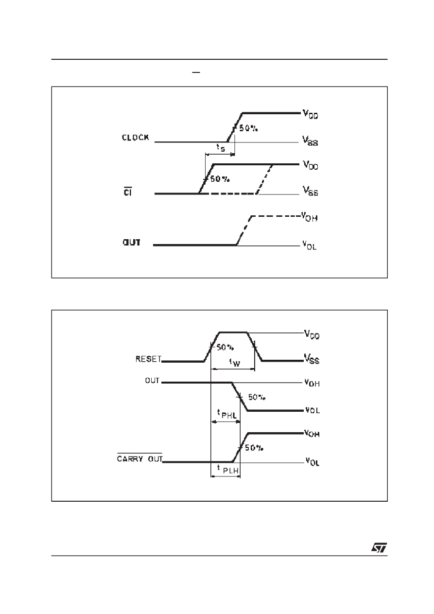
WAVEFORM 2 : MINIMUM SETUP TIME (CI TO CLOCK) (f=1MHz; 50% duty cycle)
WAVEFORM 3 : PROPAGATION DELAY TIMES, MINIMUM RESET PULSE WIDTH (f=1MHz; 50%
duty cycle)
HCF4516B
9/11
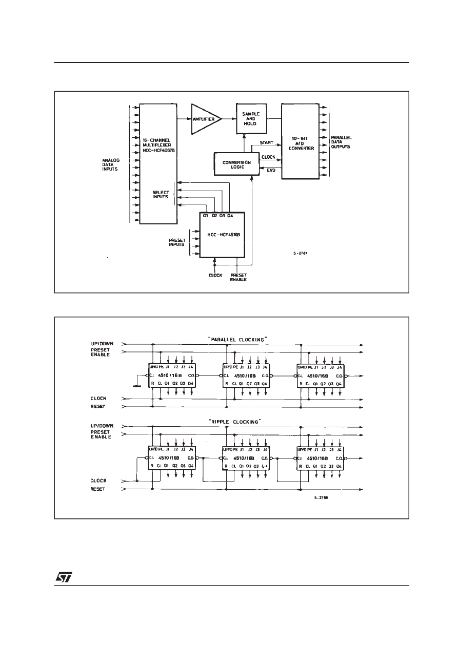
TYPICAL APPLICATIONS TIPICAL 16 CHANNEL, 10 BIT ACQUISITION SYSTEM
TYPICAL APPLICATIONS CASCADING COUNTER PACKAGES
HCF4516B
10/11
Information furnished is believed to be accurate and reliable. However, STMicroelectronics assumes no responsibility for the
consequences of use of such inform ation nor for any infringe ment of patents or other righ ts of third parties which may result from
its use. No license is granted by implication or otherwise under any patent or patent rights of STMicroelectronics. Specifications
mentioned in this pub lication are subject to change without notice. Thi s pub lication supersedes and replaces all information
previously supplied. STMicroelectronics prod ucts are not authori zed for use as critical components in life suppo rt devices or
systems without express written approval of STMicroelectronics.
The ST logo is a registered trademark of STMicroelectronics
2001 STMicroelectronics - Printed in Italy - All Rights Reserved
STMicroelectronics GROUP OF COMPANIES
Australia - Brazil - China - Finland - France - Germany - Hong Kong - India - Italy - Japan - Malaysia - Malta - Morocco
Singapore - Spain - Sweden - Swit zerland - United Kingdom
http://w ww.st.com
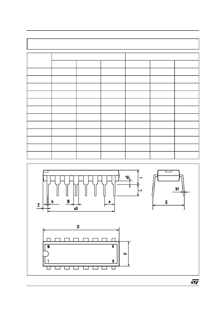
DIM.
mm.
inch
MIN.
TYP
MAX.
MIN.
TYP.
MAX.
a1
0.51
0.020
B
0.77
1.65
0.030
0.065
b
0.5
0.020
b1
0.25
0.010
D
20
0.787
E
8.5
0.335
e
2.54
0.100
e3
17.78
0.700
F
7.1
0.280
I
5.1
0.201
L
3.3
0.130
Z
1.27
0.050
Plastic DIP-16 (0.25) MECHANICAL DATA
P001C

HCF4516B
11/11
Information furnished is believed to be accurate and reliable. However, STMicroelectronics assumes no responsibility for the
consequences of use of such information nor for any infringement of patents or other rights of third parties which may result from
its use. No license is granted by implication or otherwise under any patent or patent rights of STMicroelectronics. Specifications
mentioned in this publication are subject to change without notice. This publication supersedes and replaces all information
previously supplied. STMicroelectronics products are not authorized for use as critical components in life support devices or
systems without express written approval of STMicroelectronics.
The ST logo is a registered trademark of STMicroelectronics
2002 STMicroelectronics - Printed in Italy - All Rights Reserved
STMicroelectronics GROUP OF COMPANIES
Australia - Brazil - Canada - China - Finland - France - Germany - Hong Kong - India - Israel - Italy - Japan - Malaysia - Malta - Morocco
Singapore - Spain - Sweden - Switzerland - United Kingdom - United States.
http://www.st.com
Wyszukiwarka
Podobne podstrony:
4516
4516
4516
4516
4516
4516
4516 ac
a lot of various circuits index 1628613 25 4516
więcej podobnych podstron