
1
PASSIVE PFC FOR FLYBACK CONVERTORS
Parviz Parto and Keyue M. Smedley
Dept. of Electrical and Computer Engineering
University of California, Irvine
Irvine, California 92697
Abstract—A new passive Power Factor Corrector
(PFC) based on Valley Fill (VF) is proposed for an off-line
Flyback converter. By adding an extra winding which is
magnetically coupled to the Flyback transformer and
electrically coupled to the VF, higher Power Factor (PF)
and lower Total Harmonic Distortion (THD) can be
achieved. The proposed circuit uses a high frequency
inductor, low voltage capacitors that operate at a voltage
slightly higher then the half of the peak line voltage, and a
low stress switch for DC/DC conversion. Since it is
passive an active switch for PFC functions is not
necessary. The paper describes the proposed circuit in
detail followed by experimental results.
I. INTRODUCTION
Conventional diode rectifiers draw input current in
short pulses rather then smooth sine waves, which
causes harmonics distortion and low power factor. This
pulsed input current pollutes the power systems,
interfere neighbouring appliance, and impose high
voltage and current stress to the DC/DC converters.
Many agencies have set international standards to
regulate the input current of electronic products. In
order to fulfil the standards, numerous Power Factor
Correction (PFC) methods have been proposed in
recent years.
Power factor improvement circuits can be achieved
by active and passive means. A typical active two stage
PFC circuit uses a boost converter followed by a
DC/DC converter to regulate the output voltage with a
DC link at higher voltage than the peak of the AC
supply. The active PFC circuit is entirely satisfactory
for harmonics compliance but the design complexity
and cost of the additional circuitry is often
unacceptable in low power applications.
The single-stage active PFC integrates two power
stages into one, but the high switch stress and the use
of high voltage capacitor are some of the drawbacks.
The passive PFC circuits operate at the line
frequency and use capacitors and inductors in a low
pass or band pass configuration. This solution offers a
trade-off between the cost and performance.
Unfortunately, the physical size and weight of this filter
makes it unattractive for compact solutions.
Another way to achieve passive power factor
improvement is by a circuit called “Valley Fill”, which
mostly used in the electronic ballast as PFC.
In this paper, a new single-stage Flyback converter
suitable for low power application with Improved
Valley Fill (IVF) as power factor corrector is
introduced. The new converter uses an extra winding
that is magnetically coupled to the Flyback transformer
and electrically coupled to the Valley Fill capacitors. A
high frequency inductor is employed to suppress the
charging spikes at the peaks of the current wave and
achieve lower total harmonic distortion (THD).
Section II provides a review of various conventional
passive PFC methods. The principle of the proposed
circuit is given in Section III, Section IV illustrates the
experimental results. Further improvement with
experiment results has been shown in Section V,
Section VI discuses the output voltage ripples and
finally conclusions are given in Section VII.
II. REVIEW OF PASSIVE PFC METHODS
A frequently used passive PFC is a LC-network,
which works at the line frequency and has been
thoroughly described in literature. There are many
possible positions for placing the capacitors and
inductors, as discussed in [1], [2]. An extension has
been shown in [3], by adding an extra capacitor and
one diode, which is, called “LCD” rectifier. The
improvement leads to smaller inductance and
consequently smaller magnetic core and causes the
equipment to change the class from D to A according
to the EN61000-3-2 Standards [4].
The other passive PFC solution is the conventional
Valley Fill which is frequently used in electronic
ballast applications. The circuit contains two capacitors
and three diodes. The two electrolytic capacitors are
charged in series around the line peak to a half of the
peak line voltage. As long as the line voltage remains
above single capacitor voltage, the line feeds the load
directly. When the line voltage falls below the single
capacitor voltage, the bridge rectifier diodes are
reversely biased, and Valley Fill’s diodes conduct and
the capacitors are connected in parallel to feed the
load.
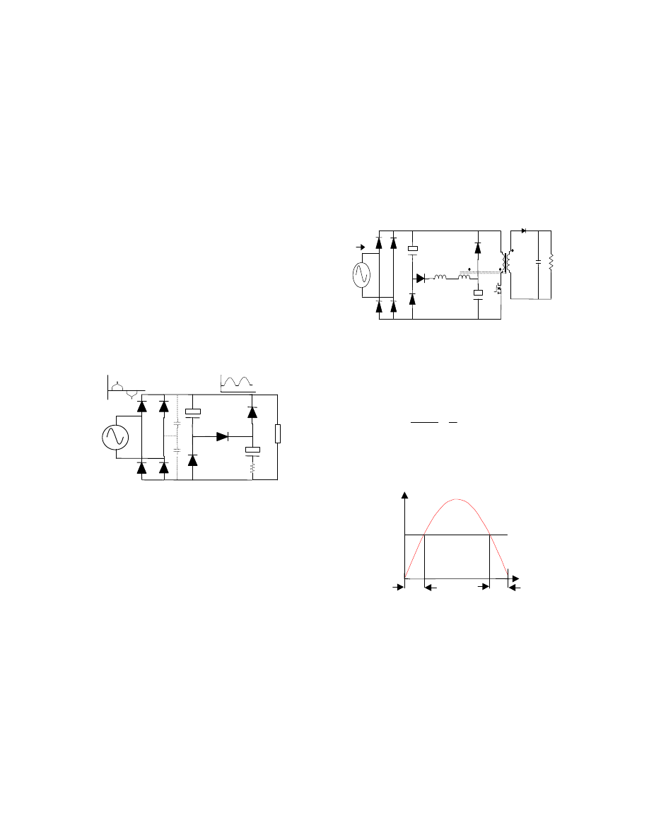
Figure 1 shows a conventional Valley Filled circuit
and its waveforms, the spike at the peak of input
2
current is a result of charging the capacitors at the peak
line voltage. This spike and the cross over distortion
are reflected to AC side as alternating current pulses
and associated harmonics.
To improve the basic Valley Fill circuit, an inductor
can be added in front of bridge or charging leg to
smooth out the peak of input current due to the abrupt
charging of the two capacitors [5]. However, the
penalty is again the addition of a line frequency
inductor.
Another solution has been presented in [6] to reduce
the charging current spike by inserting a resistor R
1
in
to the bottom electrode of C
2
(see figure 1, dashed
components) and adding a voltage doubler to extending
the input current conduction angle. A higher power
factor and lower THD can be achieved, but the
drawback is lower efficiency, due to losses at the
resistor R
1
. The losses can be slightly reduced if
resistor R
1
is inserted in the diode D
1
branch instead.
A resonant based improvement of Valley Fill circuit
was reported in [7] for light ballast applications where
a resonant current was injected in to the Valley Fill
circuit to improve the input current waveform.
C
1
C
2
D
1
D
2
D
3
V
g
V
g
/2
V
g
C
3
C
4
R
1
i
g
Load
V
DC-bus
Fig.1 the original Valley Fill and its waveforms
The objective of this paper is to develop an
improved valley fill method for a PWM converter (i.e.
Flyback) to achieve low input distortion and high
power factor at a low cost.
The advantage of the proposed circuit is that it uses
low voltage capacitors that operate at a voltage slightly
over the half of input voltage and high frequency
inductor. No additional switch is needed to perform
PFC function and no additional voltage and current
stresses are added to the DC/DC converter switch.
Therefore it is a cost-effective solution and provides
less stress over the DC/DC converter. The parallel
combination of capacitors also can provide the hold-up
voltage to DC/DC converter during the time when
input voltage is low.
III. THE PROPOSED CIRCUIT
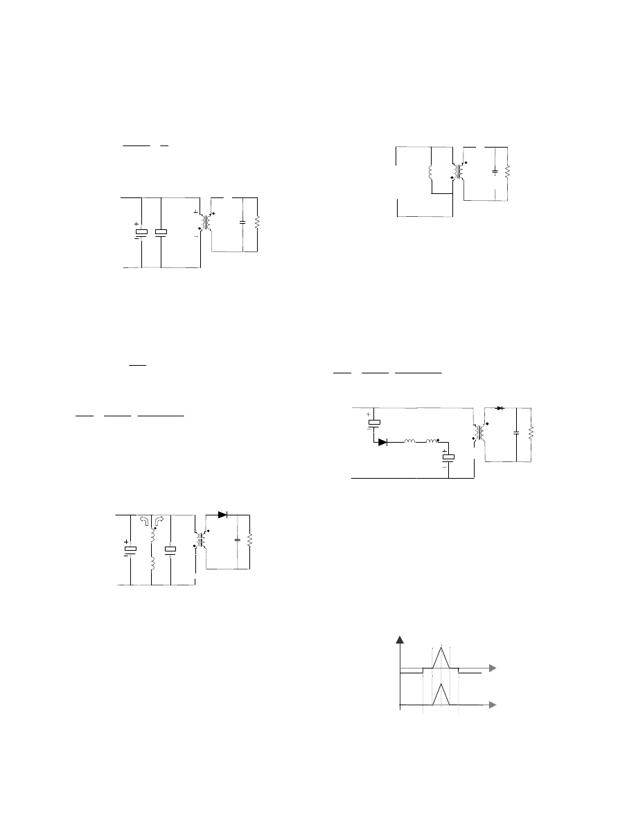
The functional diagram of the proposed circuit is
shown in Figure 2. The converter operates under both
low (line) and high (switching) frequency. The circuit
contains two electrolytic capacitors (C
1
, C2), three
diodes (D
1
, D
2
and D
3
), an inductor (L
1
) and an extra
winding (N
2
), which is magnetically coupled to the
Flyback transformer and electrically coupled to valley
fill capacitors. L
1
and N
2
connected in series with the
capacitors in charging path to smooth out the peaking
of input current. The inductor L
1
operates at the high
frequency, which means small size and relatively low
cost. In the following analysis, it is assumed that the
switch and diodes are ideal.
C
1
D
1
D
3
C
2
D
2
D
4
V
g
Q
T
N
1
N
3
C
o
R
L
i
g
V
c
V
c
V
o
N
2
+
+
+
+
L
1
+
_
V
L1
V
N
V
N
+
_
_
_
_
_
V
DC--bus
Fig.2 the proposed circuit for Flyback converter
The operation of the Flyback converter is well known
so it is not repeated here. It is assumed that the
converter operates beyond the boundary condition
(CCM and DCM), thus the output voltage is given by:
n
D
D
V
V
bus
DC
o
1
1
∗
−
∗
=
−
(1)
where V
o
is output voltage, V
DC-bus
is primary voltage,
D is duty cycle and n is Flyback transformers turns
ratio N
1
/N
3
. The operation consists of two modes in a
half of a line cycle.
V
g
t
V
c
M
1
M
2
M
1
Fig3.Tthe operating modes in half of a line cycle
Operating mode M
1
:
0 < V
g
< V
c
The input voltage starts from zero crossing of the input
voltage. Since
g
c
V
V
〉
the rectifier diodes are reverse-
biased, the valley fill capacitors (C
1
, C2) are connected
via D
1
and D
2
in parallel to provide energy to the load.
During this mode there is no input current drawn from the
AC source by the converter.
While switch Q conducts, energy from the VFs’
capacitors charges the primary inductance L
l
, and we
have:
3
c
bus
DC
V
V
=
−
(2)
During that interval there is no current through N
2
,
because diode D
4
is reverse-biased (see figure 4). The
output voltage is given by the following equation:
n
D
D
Vc
V
o
1
1
∗
−
∗
=
(3)
where V
c
is Capacitor voltage.
T
N
1
N
3
C
o
R
L
V
o
V
N1
C
2
C
1
V
c
Fig.4 Mode 1, Vc>V
g
and Q
1
is on
When switch Q is off, the diode D
4
conducts and the
stored energy transfers to the load.
If
c
g
N
V
V
V
2
2
〈
+
(4)
3
2
2
*
N
N
V
V
o
N
=
(5)
By combining (3) and (5), condition (4) becomes:
1
2
1
1
2
≈
−
〈
−
∗
c
g
c
V
V
V
D
D
N
N
(6)
Under this condition, there is no current through N
2
.
If:
c
g
N
V
V
V
2
2
〉
+
(7)
the current starts to flow through N
2
and L
1
and charges
C
1
and C
2
. Figure 5 shows the equivalent circuit.
N
1
V
c
C
1
C
2
N
2
T
N
3
D
4
C
o
R
L
V
o
L
1
Fig.5 Mode 1, switch Q is off and V
N2
+Vg>2V
C
The voltage stress across switch Q during mode 1 is
given by:
n
V
Vc
V
o
Q
+
=
where V
Q
is voltage across switch, V
c
is capacitor
voltage, V
o
is output voltage and n is the turns ratio
N
1
/N
3
.
Operating mode M
2
:
V
g
>V
c
When the magnitude of the input voltage increases
above V
c
, the line directly supplies energy to the
Flyback. When transistor Q is on, the primary winding
inductance of transformer is charged by the input
voltage V
DC-bus
= V
g
.
T
N
1
N
3
C
o
R
L
V
o
L
l
V
g
+
_
V
N1
Fig.6 Mode 2, V
g
>V
c
and Q
1
is on
The stored energy transfers to the output when
transistor Q
is off and
diode D
4
conducts. There is no
current through N
2
if:
c
g
N
V
V
V
2
2
〈
+
(4)
The capacitors are being charged through N
2
(see
figure 7) when:
c
g
N
V
V
V
2
2
〉
+
(8)
1
2
1
1
2
≈
−
〉
−
∗
g
g
c
V
V
V
D
D
N
N
(9)
D
4
C
1
D
3
C
2
T
N
1
C
o
R
L
V
c
V
c
V
o
N
2
N
3
L
1
Fig.7 Mode2, 2V
c
<V
g
<V
c
and Q
is off and C
1
, C
2
charge
through N
2
and L
1
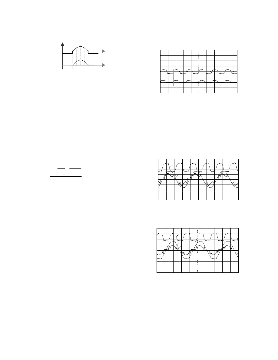
Equation (9) shows that the extra winding pulls current
from input to charge the capacitors. In contrast, the
original Valley Fill charges the capacitors only at the
peak of input voltage. Figure 8 shows the theoretically
current waveforms through the capacitors (I
c
) and
charging leg (I
D3
) of original Vally Fill circuit. The
correspondent currents for the Improved Valley Fill
with extra winding (proposed circuit) are shown in
figure 9.
I
c
I
D3
M
1
M
2
t
t
Fig.8 I
c
and I
D3
for en original Valley Fill
4
I
c
I
D3
M
1
M
2
t
t
Fig.9 I
c
and I
D3
for the proposed circuit
By adjusting the turns ratio between the two
windings N
1
and N
2
, the voltage across the capacitors
can be controlled. In this case, the capacitors voltage is
slightly higher than half of the peak line voltage; as a
result, the current peak is reduced. If the winding N
2
is
too high such that the capacitor voltage is much higher
than a half of the peak input voltage. The non-
conduction angle will be larger which results in higher
THD. The non-conduction angle is directly related to
the capacitor voltage and input voltage and can be
expressed as follows:
α
Sin
V
V
g
c
∗
=
(10)
Eq. (11) shows
α as a function of N
2
/N
1
and duty cycle
D.
2
1
1
1
2
D
D
N
N
Sin
−
∗
+
=
αα
(11)
where
α is the non-conduction angle of input current.
An important note is that it is necessary to have both
N
2
and L
1
in the charging path. N
2
provides an early
charging of capacitors, and acts as an extra voltage
source, while L
1
smooth out the current. The using of
L
1
also results in a lower output ripple.
The maximum voltage stress across switch Q occurs
during this mode is given by:
n
V
Vg
V
o
Q
+
=
(12)
where V
Q
is voltage across switch, V
g
input voltage, V
o
output voltage and n is N
1
/N
3
.
Equation (12) shows
that the new circuit doesn’t cause additional
stress to the switch, thus the switch stress will
be the same as that of a regular Flyback.
IV. EXPERIMENTAL RESULTS
The proposed circuit of figure 2 has been prototyped
and tested in the laboratory. The prototype is designed
for a 50kHz Flyback with following component data:
C
1
, C
2
= 150
µF, C
o
=200
µF, N
2
/N
1
=[0, 0.25 and 1],
L
1
=200
µ
H, P
out
=50W. The line voltage is 110V
ac
, 60
Hz. Efficiency measured on a 50 W power supply is
only slightly (1%) less then the Flyback converter with
conventional diode rectifiers. Figure 10 shows the
measured currents through the Valley Fill capacitor I
c1
and charging leg I
D3
with N
2
/N
1
=1.
M 1
M 2
G N D (1)
G N D (2)
1
Fig.10 The measured I
c1
and I
D3
for the proposed circuit
1):I
c1
(1A/div), 2):I
D3
(1A/div)
Horizontal scale (5 ms/div)
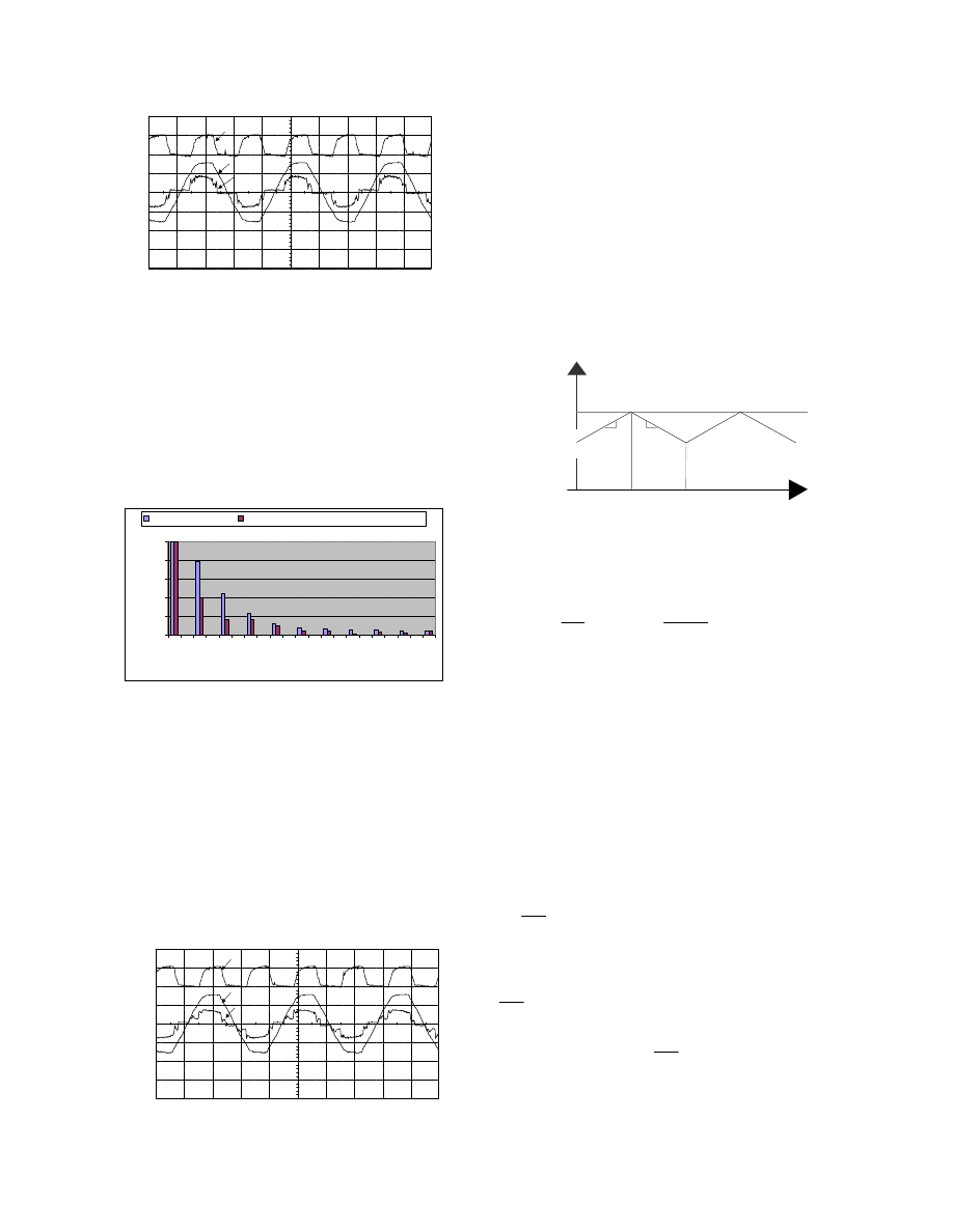
As figure 10 shows the capacitors are charged up
smoothly when Mode 2 starts and there is no spike at
the peak. Figures 11-13 show the experimental
waveforms of DC-bus voltage, input voltage and input
current, measured at closed loop with a different turns
ratio N
2
/N
1
.
(G N D )
1
2
3
Fig.11 1)V
dc-bus
(50V/div),
, 2)input voltage (100V/div), and
3)input current (1A/div), with N
2
/N
1
=0 and Closed loop,
THD=42%
Horizontal scale (5 ms/div)
(G N D )
1`
2
3
Fig.12 1)V
dc-bus
(50V/div), 2)input voltage (100V/div), and
3)input current (1A/div), with N
2
/N
1
=0.25 and Closed loop,
THD=38%
Horizontal scale (5 ms/div)
5
(G N D )
1
2
3
Fig.13 1)V
dc-bus
(50V/div), 2)input voltage (100V/div), and
3)input current (1A/div), with N
2
/N
1
=1 and Closed loop,
THD=33%
Horizontal scale (5 ms/div)
The results show how varying the N
2
/N
1
ratio can
control the DC-bus voltage and AC line current and
consequently improves the input current shape form to
satisfy the harmonics standard. Figure 14 shows the
measured harmonics of input current compared with
EN 6100-3-2 class D.
0
20
40
60
80
100
1 2 3 4 5 6 7 8 9 10 11 12 13 14 15 16 17 18 19 20 21
nth Harmonics
% of Input Current
EN 61000-3-2 Class D
The measured harmonics of the propsed Circuit
Fig.14. Input current and its harmonics compering to the EN
61000-3-2 Class D at N
2
/N
1
=1
V. FURTHER IMPROVMENT
To further improve the proposed circuit, a voltage
doubler according to [6] can be applied. (See figure 1,
dashed capacitors C
3
and C
4
). The extra current path,
created by two small capacitors, causes the current to
start at zero crossing, and extend the conduction angle,
which results in lower THD. Figure 15 shows the input
current with a voltage doubbler. The measured THD
have been reduced to 23%.
1
2
3
(G N D )
Fig.15 1)V
dc-bus
(50V/div), 2)input voltage (100V/div), and
3)input current (1A/div), with N
2
/N
1
=1 and Closed loop,
THD=23%
Horizontal scale (5 ms/div)
VI. OUTPUT VOLTAGE RIPPLE
Current programmed control scheme has been used
for the experiments. Figure 16 shows the inductor
current waveform I
L
, of a current-mode converter being
controlled by an error voltage V
e
. The inductor current
rises with a slope m
1
and falls with a slope m
2
.
i
L
(t)
DT
s
T
s
t
i
L
(0)
V
e
m
1
m
2
Fig.16 Inductor current of a CMC
The slopes m
1
and m
2
for a Flyback converter are
given by:
p
g
L
V
m
=
1
and
P
o
L
n
V
m
*
2
=
where V
g
is input voltage, L
p
is the transformers
primary inductance, V
o
is the output voltage, n is turns
ratio of transformers, D is duty cycle and T
s
is
switching period.
This controller is unstable when converter steady-
state duty cycle D is grater than 0.5. It can be
stabilised by adding an artificial ramp to the sensed
switch current waveform. The artificial ramp can also
be adjusted to reduce the output voltage ripple. The
ripple at the input voltage will be found in the sensed
switch current.
The artificial ramp should fulfil the following
relationship:
2
2
2
m
m
m
c
〈
〈
where m
2
is the falling slope of the inductor and m
c
is
the artificial slope.
c
m
m
〈
2
2
guarantees current loop stability at duty cycle
greater than 50%, and
2
2
2
m
m
m
c
〈
〈
is for the best
possible input ripple rejection.
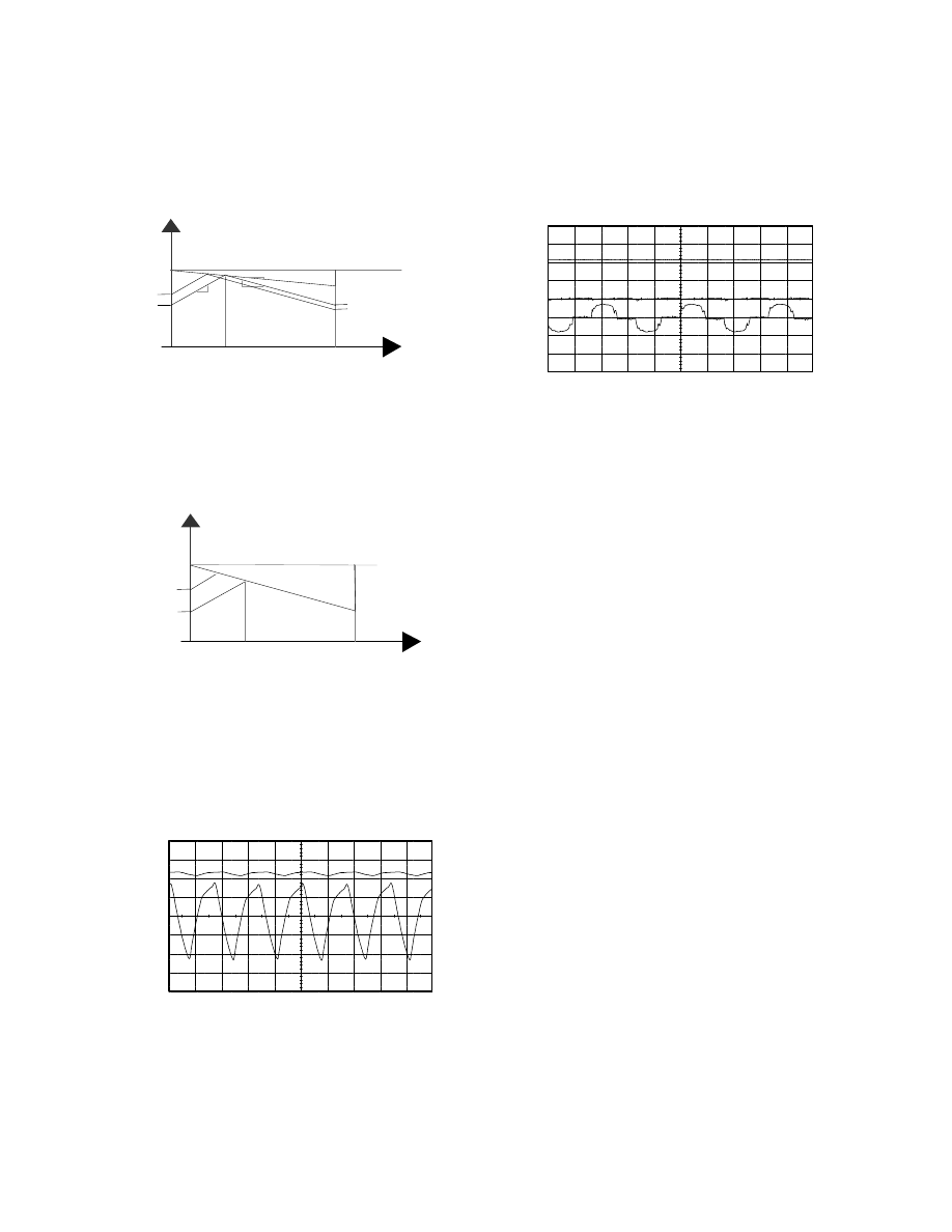
6
Figure 17 shows the inductor current waveform and
the artificial slope. It shows that any transient
∆I
caused by input voltage perturbation decreases with
time by adding a proper artificial slope.
.
i
L
(t
)
DT
s
T
s
t
i
L
(0)
V
e
m
1
m
2
m
c
∆i
0
∆i
1
Fig. 17 inductor current and the artificial slope
Figure 18 shows graphically, how a transient
perturbation is damped out in exactly one cycle when
2
m
m
c
=
.
i
L
(t)
DT
s
T
s
t
i
L
(0)
V
e
m
1
m
2
m
c
=m
2
∆i
0
Fig. 18 inductor current and the artificial slope when
mc=m2
When adjust the artificial ramp to the value in
between m
2
/2 and m
2
, the effect of the input ripple may
be minimized. Figure 19 shows the proposed circuit
measured output voltage and its ripple without artificial
slope.
.
G N D (2)
1
2
G N D (1)
Fig.19 output voltage and its ripple waveform without
artificial slope
1)V
out
(10V/div), 2)V
out
(500mV/div) ac coupled
Horizontal scale (5 ms/div)
Figure 20 shows the measured output voltage, its
ripple and input current with a tuned artificial slope
m
c
=0.82 m
2
. As shown the output ripple is reduced to
very low value without affecting the input current
shape.
G N D (3)
G N D (1)
G N D (2)
1
2
3
Fig.20 output voltage and its ripple waveform with tuned
artificial slope and input current
1)V
out
(10V/div), 2)V
out
(500mV/div) ac coupled,
3)I
in
(1A/div).Horizontal scale (5 ms/div) time
VII. CONCLUSION
A low-cost passive power factor corrector method is
introduced that combines Valley Fill with a Flyback
converter by adding an extra winding. This yields a
cost-effective solution and compliance with the
harmonics standard can be achieved. It is suitable for
low power and low cost. Experimental results have
shown an improvement in power factor and THD of
input current. The output voltage ripple can be reduced
to an acceptable level by adjusting the artificial slope
of the current control loop.
VIII. ACKNOWLEDGMENT
The authors would like to thank the members of the
Power Electronic Lab of University of California,
Irvine for many valuable discussions.
REFERENCES
[1] A. Prasad, P Ziogas, S Manias “A Novel Passive
Waveshaping Method for Single-Phase Diod Rectifiers”
IEEE Transaction on Industrial Electronics, VOL 37, NO 6,
December 1990, P521-30.
[2] R. Redl, L. Balogh “Power-Factor Correction in Bridge
and Voltage-Doubler Rectifier Circuits with Inductor and
Capacitors” APEC’95, P446-72.
[3] R. Redl “An Economical Single-Phase Passive Power-
Factor-Corrected Rectifier: Topology, Operation, Extensions,
and Design for compliance” APEC’98, P454-60
[4] Limits for Harmonic Current EN 61000-3-2 1995,
English version
[5] Jim Spangler, Anup K. Behara “Electronic Fluorescent
Ballast using a Power Factor Correction Techniques for
Loads Greater then 300 Watts” APEC’91, P393-9.
[6] K. Kit Sum “Improved Valley-Fill Passive Current
Shaper” PCIM’97, P42-50

7
[7] Yong-Sik Youn, Gyun Chae and Gyu-Hyeong Cho”A
Unity Power Factor Electronic Ballast for Fluorescent Lamp
having Improved Valley Fill and Valley Boost Converter”
PEPSC’97, P53-9.
.
Wyszukiwarka
Podobne podstrony:
więcej podobnych podstron