1
1
2
2
3
3
4
4
D
D
C
C
B
B
A
A
Title
Number
Revision
Size
Letter
Date:
3/14/2007
Sheet of
File:
C:\Program Files\..\Chopper_A.SchDoc
Drawn By:
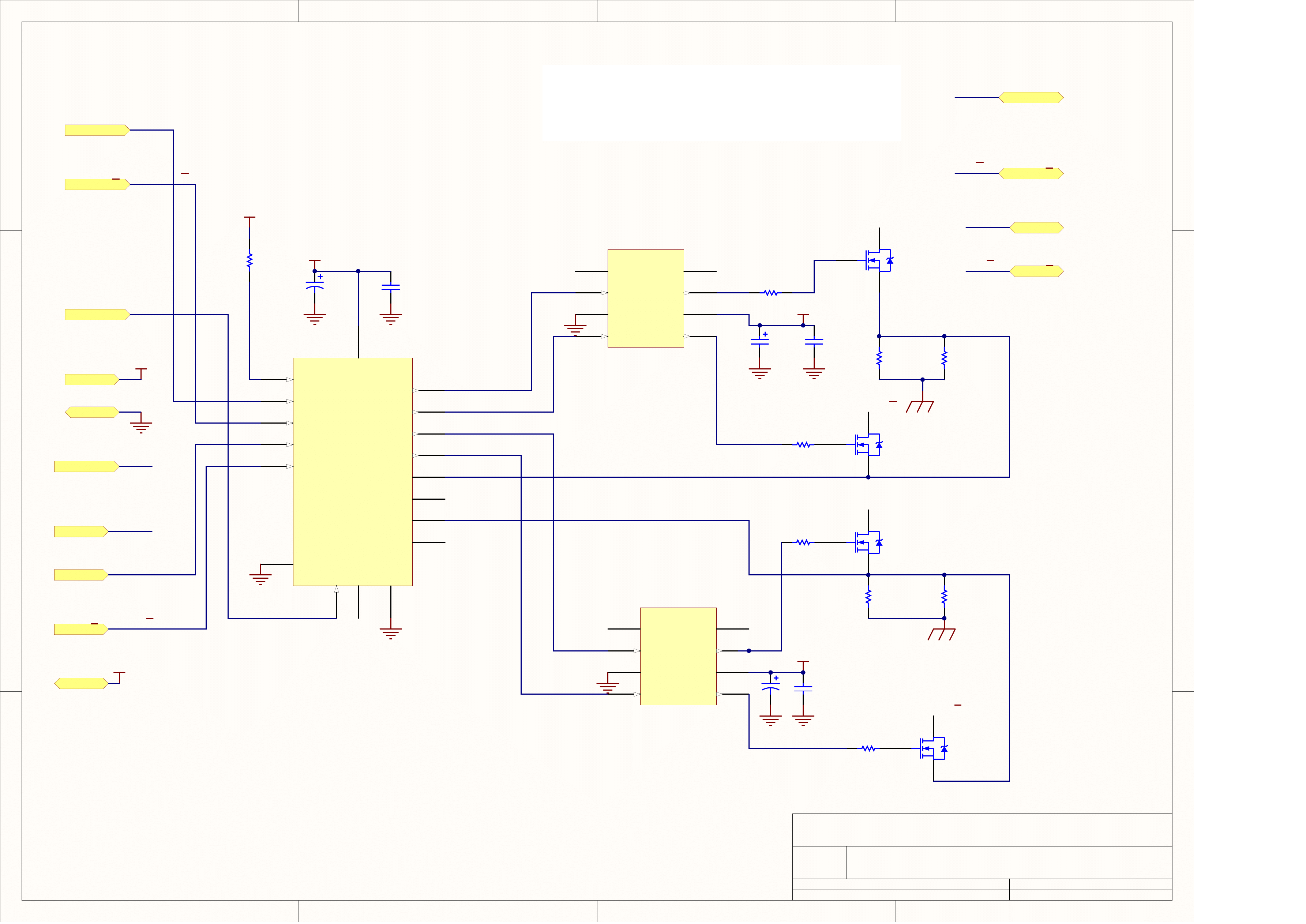
R10
47
R11
47
Q1
IRL640
Q2
IRL640
R14a
0.2 Ohm 5 Watt
Vsense1
Coil_A
Coil_A
VREF1
VCC
Phase_A
Phase_A
VREF1
COIL_A
COIL_A
VREF1
Phase _A
Phase _A
Coil_A
Coil_A
C12
10 uF 16 Volt
MARDUS-KREUTZ CHOPPER WITH L6506
KREUTZ
0.00
SYNC
SYNC
VCC
GND
VCC
C13
0.1 uF Ceramic
C16
0.1 uF
R14
0.2 Ohm 5 Watt
2/3
Use IRL640 logic input power MOSFETS
The 47 ohm (1/8 watt) gate resistor value is subject to change depending on
Turn-on and Turn-off times of the chosen mosfet, a resistor is often
necessary in order to suppress ringing
C11
10 uF 16 volt
VDD
R/C
1
O
S
C
2
S
y
n
c
3
Pwr EN
4
In1
5
In2
6
In3
7
In4
8
G
N
D
9
Vs1
10
Vs2
15
Ref1
16
Ref2
17
Out4
11
Out3
12
Out2
13
Out1
14
V
C
C
1
8
U4
L6506
VREF2
Phase_B
Phase_B
Phase_B
Phase_B
VREF2
VREF2
Q3
IRL640
Q4
IRL640
R15
0.2 Ohm 5 Watt
R15a
0.2 Ohm 5 Watt
Coil_B
Coil_B
R12
47
R13
47
VCC
R9
10k
COIL_B
COIL_B
Coil_B
Coil_B
NC
1
INA
2
GND
3
INB
4
OUTB
5
VDD
6
OUTA
7
NC
8
U5
TC427CPA
NC
1
INA
2
GND
3
INB
4
OUTB
5
VDD
6
OUTA
7
NC
8
U6
TC427CPA
VDD
C15
0.1 uF ceramic
C14
10 uF 16 Volt
VDD
VDD
Vsense2
1
1
2
2
3
3
4
4
D
D
C
C
B
B
A
A
Title
Number
Revision
Size
Letter
Date:
3/14/2007
Sheet of
File:
C:\Program Files\..\Input-Power.SchDoc
Drawn By:
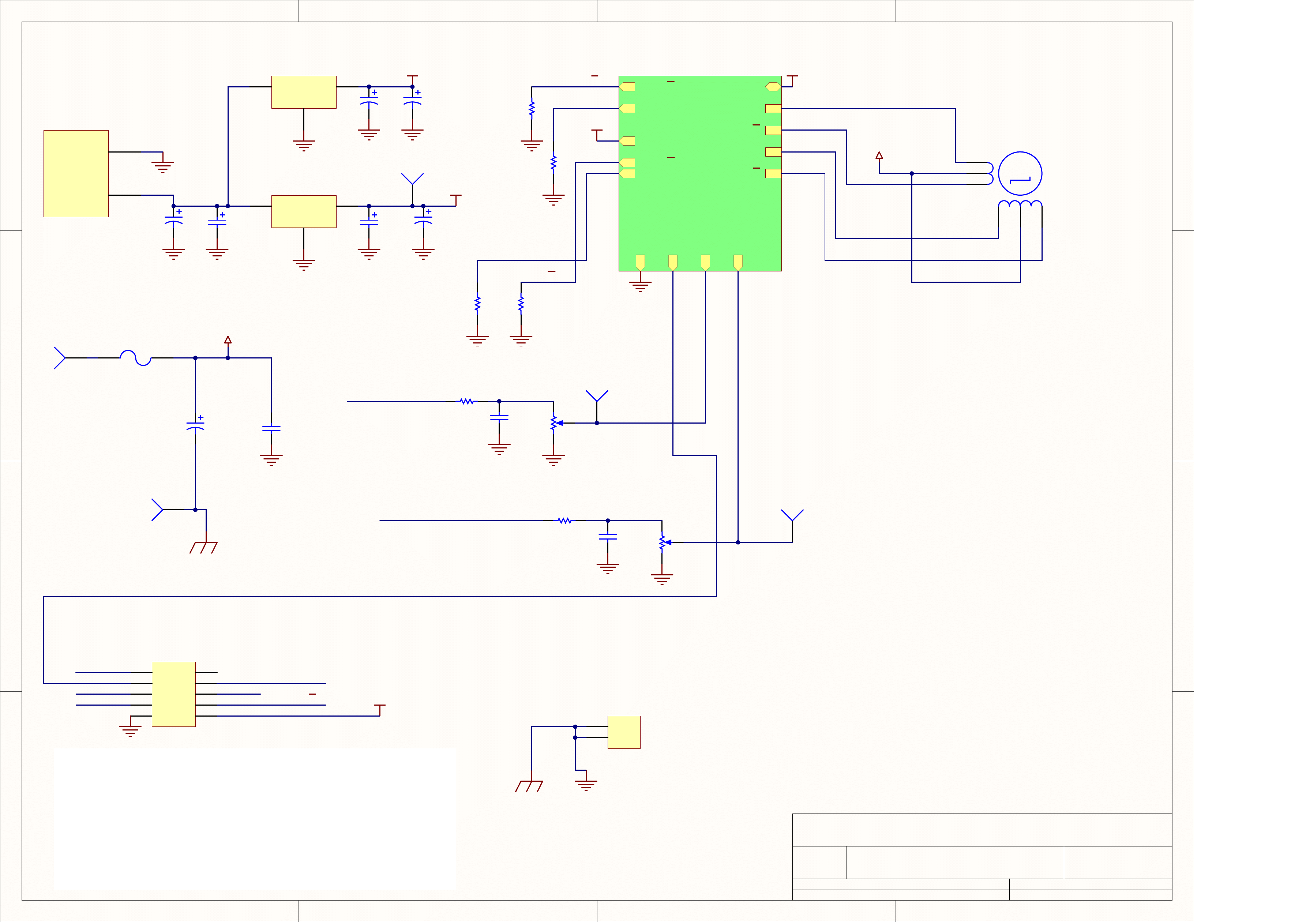
IN
1
2
OUT
3
GND
U8
MC7805BT
C1
100 uF 25 volt
C4
10 uF 16 volt
VCC
C3
1 uF
C2
1 uF
VMotor
J1
Socket
J2
Socket
C7
470 uF 160 volt
VCC
M
Motor Stepper
VMotor
MARDUS-KREUTZ UNIPOLAR STEPPER DRIVER WITH L6506
0.00
KREUTZ
+12 TO +15 VOLT DC INPUT
+80 VOLT MAX
POWER GROUND
1
2
3
4
5
6
7
8
9
10
P4
Header 5X2
VCC
Phase_A
Phase_A
Phase_B
Phase_B
VREF_Channel A
VREF_Channel B
VREF2
VREF1
Phase_A
Phase_B
Phase_A
Phase_B
R7
5k
R8
5k
R6
10k
R5
10k
VREF_Channel A
VREF_Channel B
PowerGround
1
2
P5
Header 2
C10
0.01 uF
C9
0.01 uF
+V
+V
A
A-
B
B-
To Translator Stage
Gnd test points on the board
J?
Socket
+5 Volt
R1, R2, R3 and R4 (4.7K) pull-down resistors are required in order to avoid the output
transistors to turn on during power up or in case the translator circuit is not connected
to the board, and during the microcontroller initialization stage after reset or power up.
+12 volt must be present before powering up the +Vmotor power supply.
For 8 Amp option use 2 Oz copper FR4 pcb or beefup with solder the PCB traces
corresponding with the coil connections and +Vmotor. Replace also the 10 Amp slow
Blow fuse by 20 Amp Slow Blow Fuse. 10 Amp fuse has been calculated for 4 Amp
peak coil current. Keep the Sensor resistor's bodies separated from the PCB board by
at least 1 mm.
F1
10A T
+V
PWM filter fc ~ 1.5 khz
PWM filter fc ~ 1.5khz
1/3
TP2
TP3
R2
4.7K
R1
4.7K
R3
4.7K
R4
4.7K
VCC= 5.0 Volt
VDD
C5
100 uF 25 volt
VDD= 9 Volt
IN
1
2
OUT
3
GND
U7
L7809ABV
C6
1 uF
1
1
2
2
J3
Term. Box 2 pos
C8
1 uF Metalized Polypropylene 250 V
PB1
Phase_A
Phase_A
V
R
E
F
1
COIL_A
COIL_A
S
Y
N
C
VCC
G
N
D
V
R
E
F
2
Phase_B
Phase_B
COIL_B
COIL_B
VDD
U_Chopper_A
Chopper_A.SchDoc
VDD
1
1
2
2
3
3
4
4
D
D
C
C
B
B
A
A
Title
Number
Revision
Size
Letter
Date:
3/14/2007
Sheet of
File:
C:\Program Files\..\Translator2.f.SchDoc
Drawn By:
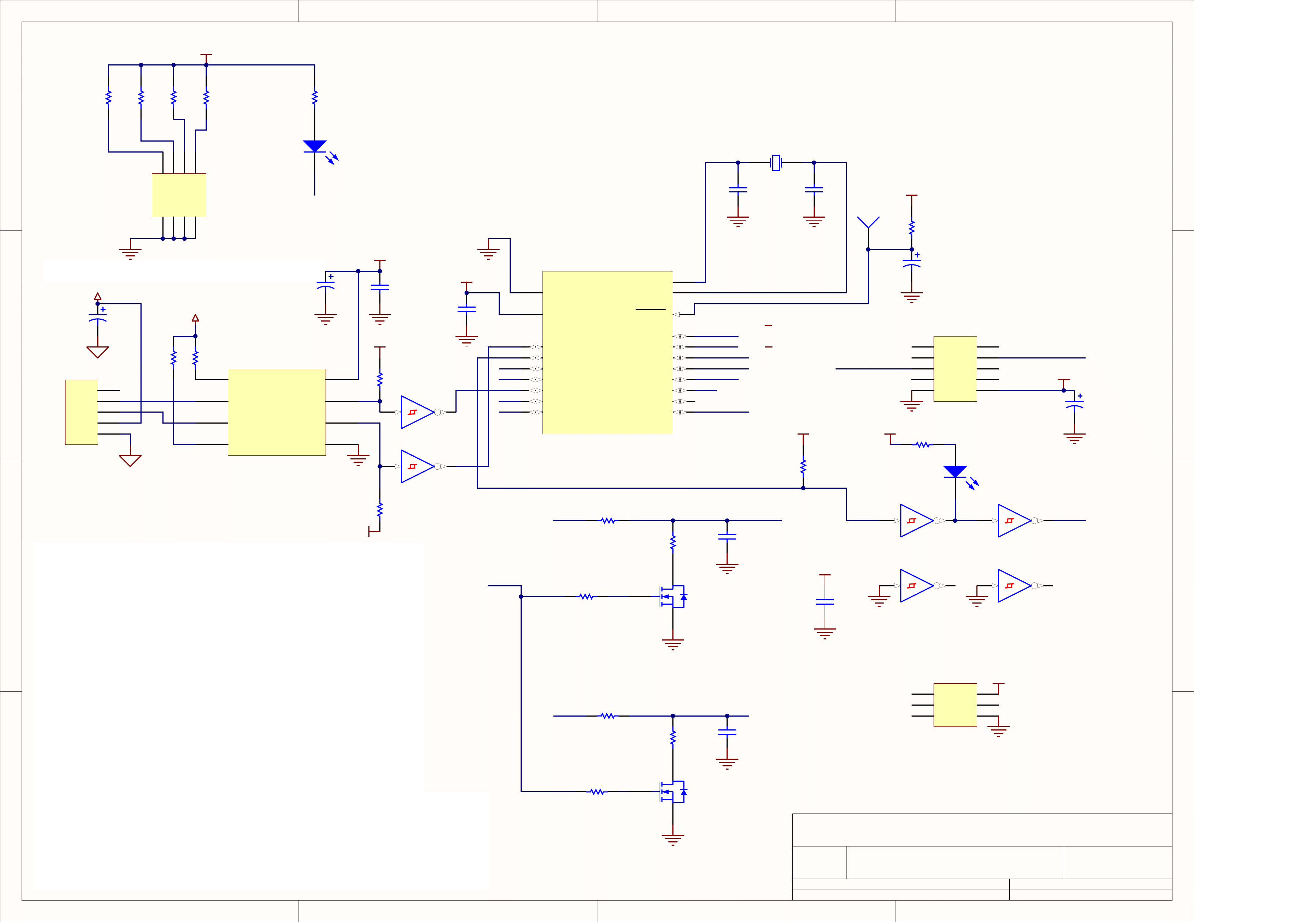
1
2
Y?
20 MHz
RESET
1
PD0 (RXD)
2
PD1 (TXD)
3
XTAL2
4
XTAL1
5
PD2 (INT0)
6
PD3 (INT1)
7
PD4 (T0)
8
PD5 (T1)
9
GND
10
PD6 (ICP)
11
PB0 (AIN0)
12
PB1 (AIN1)
13
PB2
14
PB3 (OC1)
15
PB4
16
PB5 (MOSI)
17
PB6 (MISO)
18
PB7 (SCK)
19
VCC
20
U2
ATTINY2313-20PI
1
2
U3A
M74HC14B1R
3
4
U3B
M74HC14B1R
5
6
U3C
M74HC14B1R
9
8
U3D
M74HC14B1R
11
10
U3E
M74HC14B1R
13
12
U3F
M74HC14B1R
VCC
DIR
STEP
Phase_A
Phase_A
Phase_B
Phase_B
VREF_Channel A
VREF_Channel B
1
2
3
4
5
6
7
8
9
10
P2
Header 5X2
C23
0.1 uF
C27
10 uF 16 volt
R16
10K
R17
10K
R18
10K
R19
10K
R23
10K
R24
10K
VCC
VCC
VCC
VCC
R25
10K
C26
10 uF 16 volt
PD6
PD5
PD4
PD3
PD1
PD0
Jumpers S1-1-2 to S1-5-6 binary encoded
PD3 PD1 PD0
0 0 0 Full step
0 0 1 Half step
0 1 0 1/4 Step
0 1 1 1/8 Step
1 0 0 1/16 Step
1 0 1 1/5 Step
1 1 0 1/10 Step
1 1 1 Reserved for testing and adjustment
--------------------------------------------------------------------------------------
S1-7-8 RESERVED FOR NEW FEATURES
1 Sec standby current reduction R39=R40= 1K => 50% reduction
1= OFF position
0= ON position
2.1F-00
KREUTZ
MARDUS-KREUTZ TRANSLATOR STAGE with AT TINY2313
C24
22 pF
C25
22 pF
1 Anode
1
1 Cathode
2
2 Cathode
3
2 Anode
4
GND
5
2 Output
6
1 Output
7
VCC
8
U1
HCPL2631
VCC_PC
VCC_PC
R21
330
R22
330
VCC
STEP-DIR from Breakout Board
TO MICROSTEPPER POWER STAGE
OPTO-ISOLATION STAGE
VCC
PB2
PD5
PD0
PD1
PD3
PD4
Jumper Settings
PB0
PB1
PB3
PB4
PB5
PB6
PB7
3 /3
C22
0.1 uF
STEP and DIR signals from the Printer port are "active
Low".
R20
330
DS1
RED LED
PB1
ERROR / OUTPUT DISABLE
R28
1k
R31
1k
R29
1k
R32
1k
VREF_Channel A
VREF_Channel B
R30
100
R33
100
TP1
1
2
3
4
5
6
7
8
S?
Header 4X2
Current reduction Jumper
PB2
FEATURES: 39.2 KHZ PWM Chopper frequency with programmable "Blanking time"
40 KHZ PWM type DAC for Reference 1 and Reference 2 Microstep reference waveforms.
Active Low STEP and DIRECTION optically isolated inputs.
MAXIMUM COIL CURRENTs adjustable from 0.5 TO 8 Amps.
Automatic coil current reduction after 1 seconds (selectable %)
Microstep Modes: Full, Half, 1/4, 1/5, 1/8, 1/10, 1/16
PD5A
PD5A
R26
10k
VCC
R27
330
DS2
Yellow LED
VCC
Current reduction Indicator
Q?
2N7002
Q?
2N7002
PB0
PB1
PB2
PB3
PB4
PB5
PB6
PB7
1
2
3
4
5
6
ISP
Header 3X2
VCC
PB5
PB6
PB7
RST
RST
6 PIN ISP programming interface
C28
0.1 uF
C20
1uF
1
2
3
4
5
P1
Header 5
PB1
P4 pin 5 Error/Enable output (high=Enabled)
for Standby current reduction to 68% use R29=R32= 2.2 Kohm
C29
0.1 uF
C21
2.2 uF
C30
0.1 uF
VCC
Document Outline
- Schematics
- Chopper_A.SchDoc
- Input-Power.SchDoc
- Translator2.f.SchDoc
- Components
- C1
- C2
- C3
- C4
- C5
- C6
- C7
- C8
- C9
- C10
- C11
- C12
- C13
- C14
- C15
- C16
- C20
- C21
- C22
- C23
- C24
- C25
- C26
- C27
- C28
- C29
- C30
- DS1
- DS2
- F1
- ISP
- J1
- J2
- J3
- J?
- Motor?
- P1
- P2
- P4
- P5
- Q1
- Q2
- Q3
- Q4
- Q?
- R1
- R2
- R3
- R4
- R5
- R6
- R7
- R8
- R9
- R10
- R11
- R12
- R13
- R14
- R14a
- R15
- R15a
- R16
- R17
- R18
- R19
- R20
- R21
- R22
- R23
- R24
- R25
- R26
- R27
- R28
- R29
- R30
- R31
- R32
- R33
- S?
- TP1
- TP2
- TP3
- U1
- U2
- U3A
- U4
- U5
- U6
- U7
- U8
- Y?
- Nets
- PHASE_A\
- PHASE_B\
- PHASE _A\
- COIL_B\
- COIL_A\
- +V
- COIL_A
- COIL_B
- DIR
- GND
- NetC1_1
- NetC9_2
- NetC10_2
- NetC24_2
- NetC25_2
- NetDS1_1
- NetDS2_1
- NetDS2_2
- NetF1_1
- NetMotor?_1
- NetMotor?_3
- NetMotor?_4
- NetMotor?_6
- NetP1_5
- NetP4_3
- NetQ1_1
- NetQ2_1
- NetQ3_1
- NetQ4_1
- NetQ?_1
- NetQ?_3
- NetR9_2
- NetR10_1
- NetR11_1
- NetR12_2
- NetR13_2
- NetR21_1
- NetR22_1
- NetR23_1
- NetR24_2
- NetU2_6
- NetU3_10
- NetU3_12
- NetU4_2
- NetU4_11
- NetU4_12
- NetU4_13
- NetU4_14
- NetU5_1
- NetU5_8
- NetU6_1
- NetU6_8
- PB0
- PB1
- PB2
- PB3
- PB4
- PB5
- PB6
- PB7
- PC_GND
- PD0
- PD1
- PD3
- PD4
- PD5
- PD5A
- PD6
- PHASE _A
- PHASE_A
- PHASE_B
- POWERGND
- POWERGROUND
- RST
- STEP
- VCC
- VCC_PC
- VDD
- VMOTOR
- VREF1
- VREF2
- VREF_CHANNEL A
- VREF_CHANNEL B
- VREF_CHANNEL A
- VREF_CHANNEL B
- VSENSE1
- VSENSE2
Wyszukiwarka
Podobne podstrony:
więcej podobnych podstron