HCC/HCF4063B
June 1989
4-BIT MAGNITUDE COMPARATOR
.
QUIESCENT CURRENT SPECIFIED TO 20V
FOR HCC DEVICE
.
STANDARD B-SERIES OUTPUT DRIVE
.
EXPANSION TO 8-16V...4 N BITS BY CASCAD-
ING UNITS
.
MEDIUM SPEED OPERATION : COMPARES
TWO 4-BIT WORDS IN 250ns (typ.) AT 10V
.
INPUT CURRENT OF 100nA AT 18V AND 25
°
C
FOR HCC DEVICE
.
100% TESTED FOR QUIESCENT CURRENT
.
MEETS ALL REQUIREMENTS OF JEDEC TEN-
TATIVE STANDARD N
°
13A, ”STANDARD SPE-
CIFICATIONS FOR DESCRIPTION OF ”B”
SERIES CMOS DEVICES”
DESCRIPTION
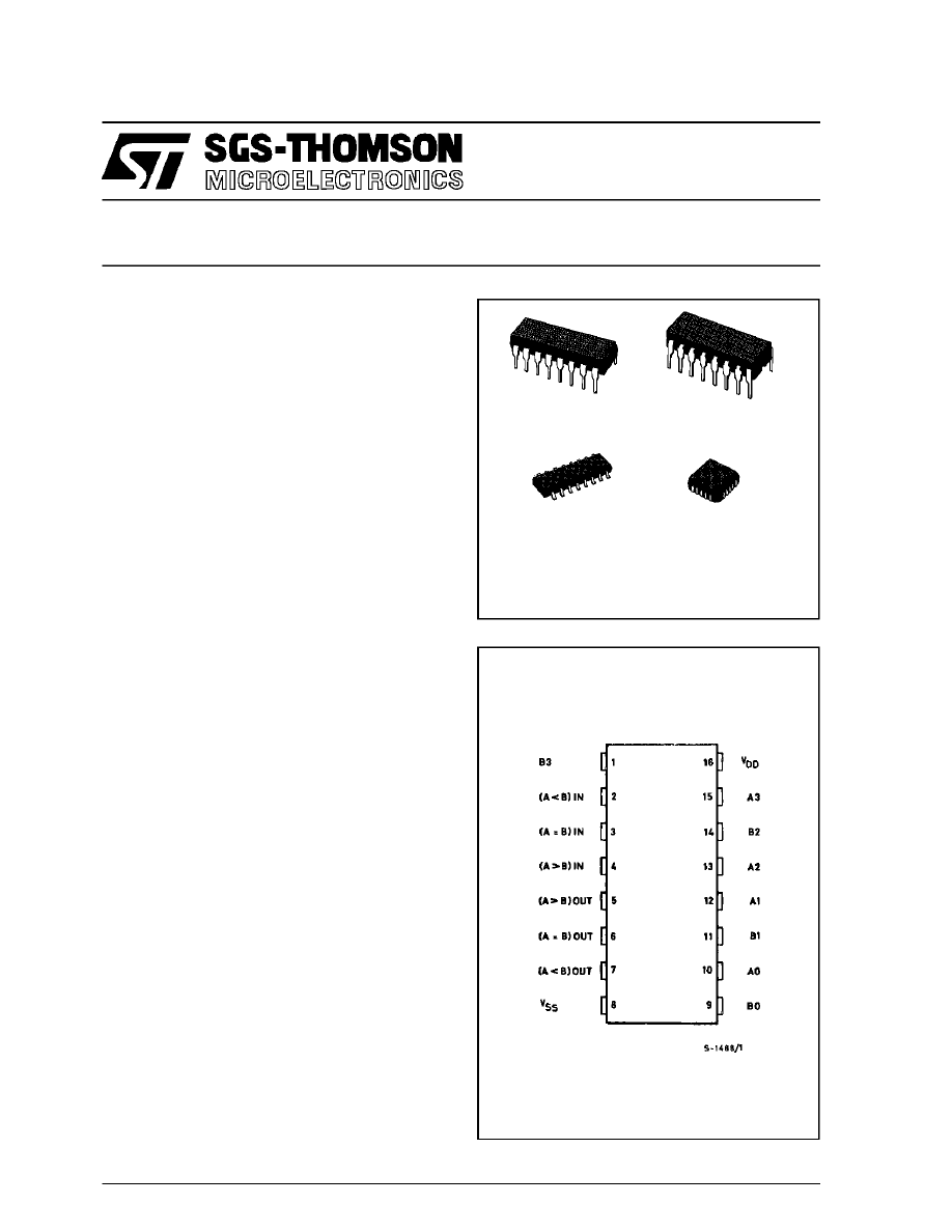
The HCC4063B (extended temperature range) and
HCF4063B (intermediate temperature range) are
available in 16-lead dual in-line plastic or ceramic
package
and
plastic
micro
package.
The
HCC/HCF4063B is a low-power 4-bit magnitude
comparator designed for use in computer and logic
applications that require the comparison of two 4-bit
words. This logic circuit determines whether one 4-
bit word (Binary or BCD) is ”less than”, ”equal to” or
”greater
than”
a
second
4-bit
word.
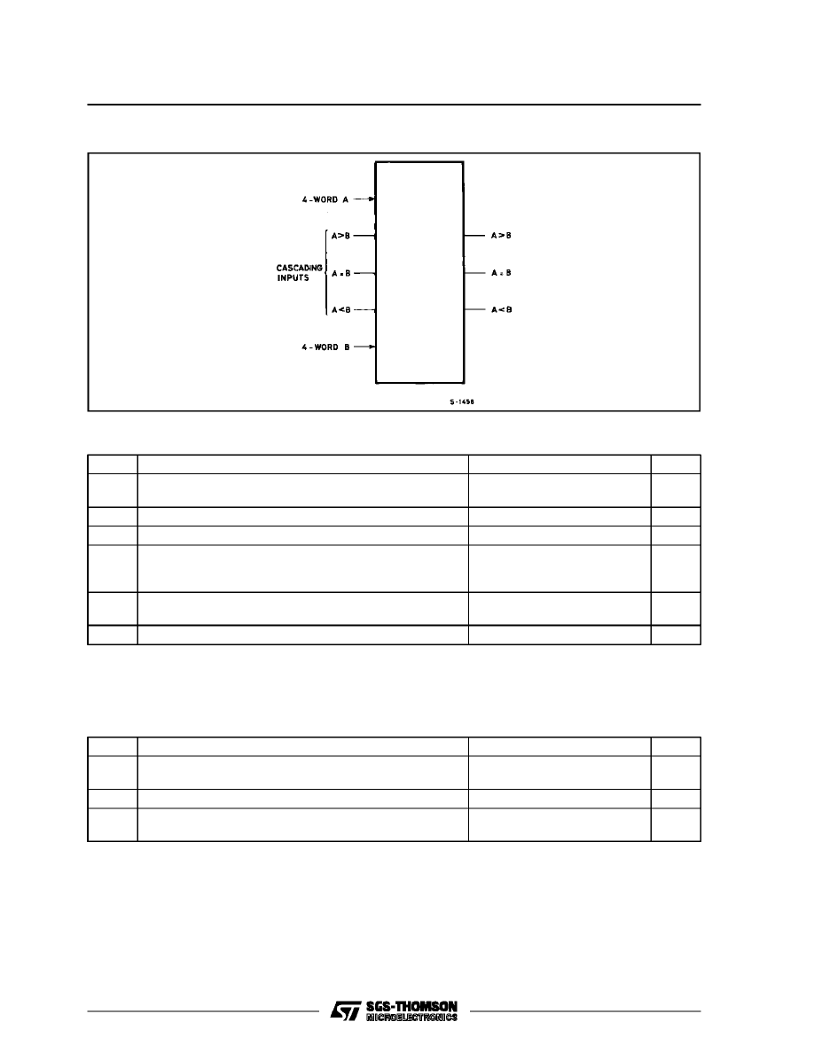
The
HCC/HCF4063B has eight comparing inputs (A3,
B3, through A0, B0), three outputs (A < B, A = B, A
> B) and three cascading inputs (A < B, A = B, A >
B) that permit systems designers to expand the
comparator function to 8, 12, 16...4 N bits. When a
single HCC/HCF4063B is used, the cascading in-
puts are connected as follows :
(A < B) = low, (A = B) = high, (A > B) = low.
For words longer than 4 bits, HCC/HCF4063B de-
vices may be cascaded by connecting the outputs
of the less-significant comparator to the correspond-
ing cascading inputs of the more-significant com-
parator. Cascading inputs (A < B, A = B, and A > B)
on the least significant comparator are connected to
a low, a high, and a low level, respectively.
EY
(Plastic Package)
F
(Ceramic Frit Seal Package)
M1
(Micro Package)
C1
(Plastic Chip Carrier)
ORDER CODES :
HCC4063BF
HCF4063BM1
HCF4063BEY
HCF4063BC1
PIN CONNECTIONS
1/12
ABSOLUTE MAXIMUM RATINGS
Symbol
Parameter
Value
Unit
V
DD
*
Supply Voltage : HC C Types
H C F Types
– 0.5 to + 20
– 0.5 to + 18
V
V
V
i
Input Voltage
– 0.5 to V
DD
+ 0.5
V
I
I
DC Input Current (any one input)
±
10
mA
P
t o t
Total Power Dissipation (per package)
Dissipation per Output Transistor
for T
o p
= Full Package-temperature Range
200
100
mW
mW
T
o p
Operating Temperature : HCC Types
H CF Types
– 55 to + 125
– 40 to + 85
°
C
°
C
T
s t g
Storage Temperature
– 65 to + 150
°
C
Stresses above those listed under ”Absolute Maximum Ratings” may cause permanent damage to the device. This is a stress
rating only and functional operation of the device at these or any other conditions above those indicated in the operational sections
of this specification is not implied. Exposure to absolute maximum rating conditions for external periods may affect device reliability.
* All voltage values are referred to V
SS
pin voltage.
FUNCTIONAL DIAGRAM
RECOMMENDED OPERATING CONDITIONS
Symbol
Parameter
Value
Unit
V
DD
Supply Voltage : HC C Types
H C F Types
3 to 18
3 to 15
V
V
V
I
Input Voltage
0 to V
DD
V
T
o p
Operating Temperature : H CC Types
H C F Types
– 55 to + 125
– 40 to + 85
°
C
°
C
HCC/HCF4063B
2/12
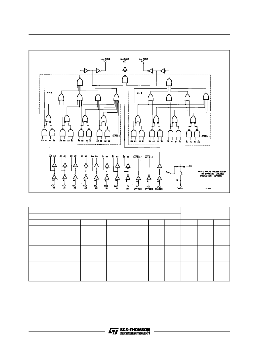
LOGIC DIAGRAM
TRUTH TABLE
Inputs
Comparing
Cascading
Outputs
A3, B3
A2, B2
A1, B1
A0, B0
A < B
A = B
A > B
A < B
A = B
A > B
A3 > B3
A3 = B3
A3 = B3
A3 = B3
X
A2 > B2
A2 = B2
A2 = B2
X
X
A1 > B1
A1 = B1
X
X
X
A0 > B0
X
X
X
X
X
X
X
X
X
X
X
X
0
0
0
0
0
0
0
0
1
1
1
1
A3 = B3
A3 = B3
A3 = B3
A2 = B2
A2 = B2
A2 = B2
A1 = B1
A1 = B1
A1 = B1
A0 = B0
A0 = B0
A0 = B0
0
0
1
0
1
0
1
0
0
0
0
1
0
1
0
1
0
0
A3 = B3
A3 = B3
A3 = B3
A3 < B3
A2 = B2
A2 = B2
A2 < B2
X
A1 = B1
A1 < B1
X
X
A0 < B0
X
X
X
X
X
X
X
X
X
X
X
X
X
X
X
1
1
1
1
0
0
0
0
0
0
0
0
X = Don’t care
1
≡
High state
0
≡
Low state.
HCC/HCF4063B
3/12
STATIC ELECTRICAL CHARACTERISTICS (over recommended operating conditions)
Test Conditions
Val ue
V
I
V
O
|I
O
|
V
D D
T
L o w
*
25
°
C
T
Hi g h
*
Symbol
Parameter
(V)
(V)
(
µ
A)
(V)
Mi n. Max. Min. Typ. Max. Min. Max.
Unit
I
L
Quiescent
Current
HCC
Types
0/ 5
5
5
0.04
5
150
µ
A
0/10
10
10
0.04
10
300
0/15
15
20
0.04
20
600
0/20
20
100
0.08
100
3000
HCF
Types
0/ 5
5
20
0.04
20
150
0/10
10
40
0.04
40
300
0/15
15
80
0.04
80
600
V
O H
Output High
Voltage
0/ 5
< 1
5
4.95
4.95
4.95
V
0/10
< 1
10
9.95
9.95
9.95
0/15
< 1
15
14.95
14.95
14.95
V
O L
Output Low
Voltage
5/0
< 1
5
0.05
0.05
0.05
V
10/0
< 1
10
0.05
0.05
0.05
15/0
< 1
15
0.05
0.05
0.05
V
IH
Input High
Voltage
0.5/4.5
< 1
5
3.5
3.5
3.5
V
1/9
< 1
10
7
7
7
1.5/13.5
< 1
15
11
11
11
V
IL
Input Low
Voltage
4.5/0.5
< 1
5
1.5
1.5
1.5
V
9/1
< 1
10
3
3
3
13.5/1.5
< 1
15
4
4
4
I
O H
Output
Drive
Current
HCC
Types
0/ 5
2.5
5
– 2
– 1.6 – 3.2
– 1.15
mA
0/ 5
4.6
5
– 0.64
– 0.51 – 1
– 0.36
0/10
9.5
10
– 1.6
– 1.3 – 2.6
– 0.9
0/15
13.5
15
– 4.2
– 3.4 – 6.8
– 2.4
HCF
Types
0/ 5
2.5
5
– 1.53
– 1.36 – 3.2
– 1.1
0/ 5
4.6
5
– 0.52
– 0.44 – 1
– 0.36
0/10
9.5
10
– 1.3
– 1.1 – 2.6
– 0.9
0/15
13.5
15
– 3.6
– 3.0 – 6.8
– 2.4
I
O L
Output
Sink
Current
HCC
Types
0/ 5
0.4
5
0.64
0.51
1
0.36
mA
0/10
0.5
10
1.6
1.3
2.6
0.9
0/15
1.5
15
4.2
3.4
6.8
2.4
HCF
Types
0/ 5
0.4
5
0.52
0.44
1
0.36
0/10
0.5
10
1.3
1.1
2.6
0.9
0/15
1.5
15
3.6
3.0
6.8
2.4
I
IH
, I
IL
Input
leakage
Current
HCC
Types 0/18
Any Input
18
±
0.1
±
10
– 5
±
0.1
±
1
µ
A
HCF
Types
0/15
15
±
0.3
±
10
– 5
±
0.3
±
1
C
I
Input Capacitance
Any Input
5
7.5
pF
* T
Lo w
= – 55
°
C for HCC device : – 40
°
C for HCF device.
* T
High
= + 125
°
C for HCC device : + 85
°
C for HCF device.
The Noise Margin for both ”1” and ” 0” level is : 1V min. with V
DD
= 5V, 2V min. with V
DD
= 10V, 2.5V min. with V
DD
= 15V.
HCC/HCF4063B
4/12
DYNAMIC ELECTRICAL CHARACTERISTICS (T
amb
= 25
°
C, C
L
= 50pF, R
L
= 200k
Ω
,
typical temperature coefficient for all V
DD
values is 0.3%/
°
C, all input rise and fall times = 20ns)
Test Conditions
Val ue
Symbol
Parameter
V
D D
(V)
Min.
Typ.
Max.
Unit
t
PL H
, t
PHL
Propagation Delay Time
Comparing Inputs to
Outputs
5
625
1250
ns
10
250
500
15
175
350
Cascading Inputs to
Outputs
5
500
1000
10
200
400
15
140
280
t
T L H
, t
THL
Transition Time
5
100
200
ns
10
50
100
15
40
80
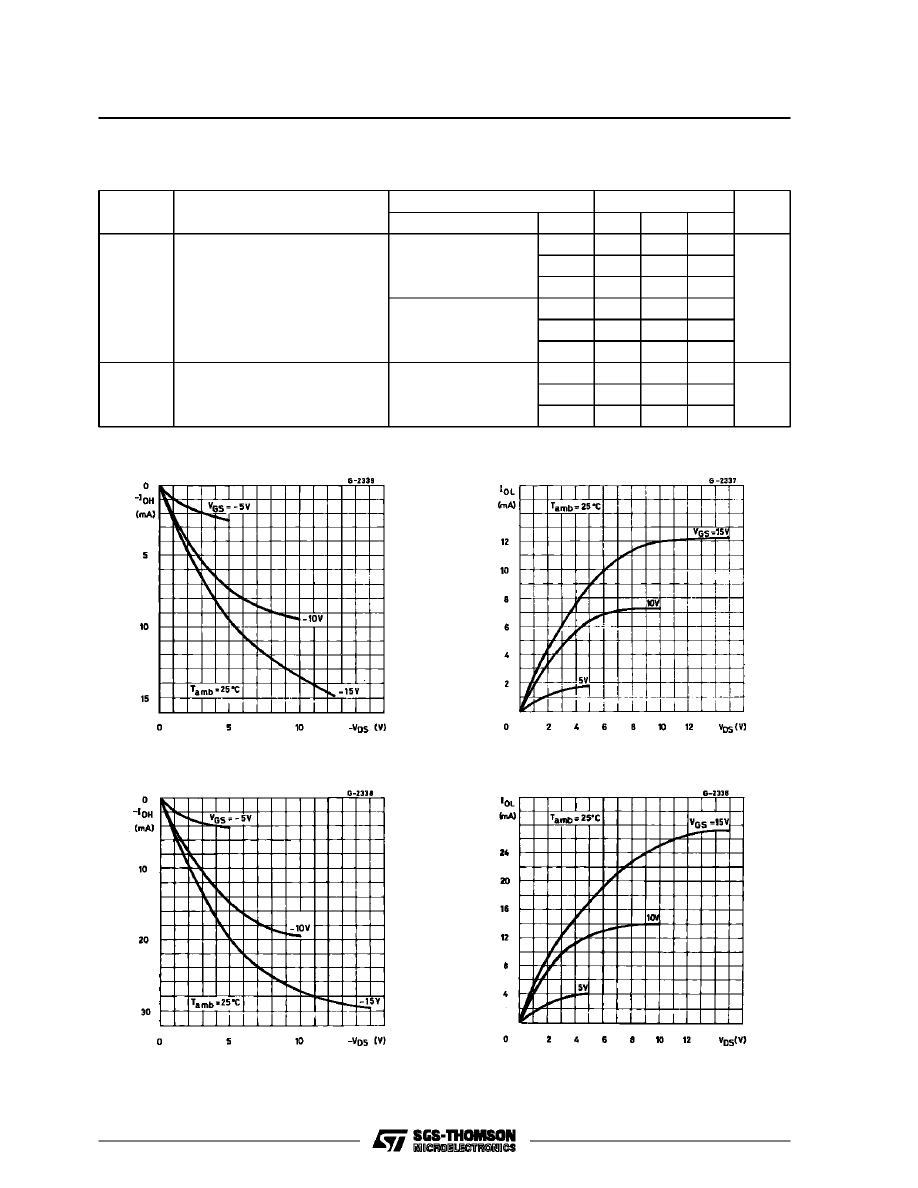
Minimum Output High (source) Current Charac-
teristics.
Minimum Output Low (sink) Current Charac-
teristics.
Typical Output High (source) Current Charac-
teristics.
Typical Output Low (sink) Current Characteristics.
HCC/HCF4063B
5/12
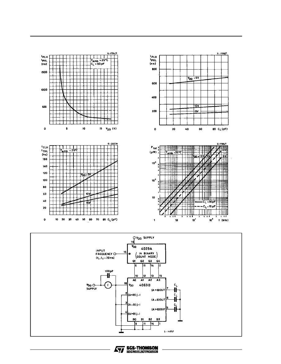
Typical Propagation Delay Time vs. V
DD
.
Typical Propagation Delay Time vs. C
L
.
Typical Transition Time vs. Load Capacitance.
Typical Power Dissipation Characteristics.
Dynamic Power Dissipation.
HCC/HCF4063B
6/12
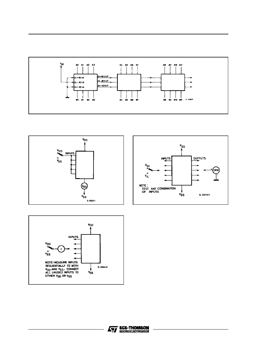
TEST CIRCUITS
Quiescent Device Current.
Noise Immunity.
Input Leakage Current.
TYPICAL SPEED CHARACTERISTICS OF A 12-BIT COMPARATOR
TYPICAL APPLICATION
t
p (TOT.)
= t
p
(COMPARE INPUTS) + 2 x t
p
(CASCADE INPUTS) at C
L
= 50pF (each output),
V
DD
= 10V (3 stages) = 250 + 2 x (200) = 650ns (typ.).
HCC/HCF4063B
7/12
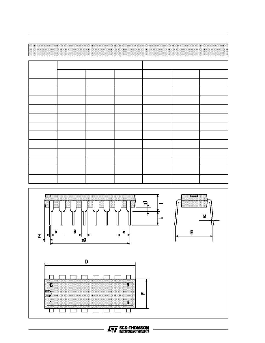
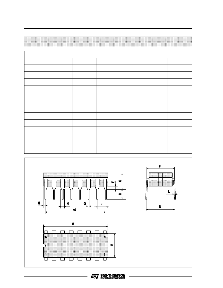
Plastic DIP16 (0.25) MECHANICAL DATA
DIM.
mm
inch
MIN.
TYP.
MAX.
MIN.
TYP.
MAX.
a1
0.51
0.020
B
0.77
1.65
0.030
0.065
b
0.5
0.020
b1
0.25
0.010
D
20
0.787
E
8.5
0.335
e
2.54
0.100
e3
17.78
0.700
F
7.1
0.280
I
5.1
0.201
L
3.3
0.130
Z
1.27
0.050
P001C
HCC/HCF4063B
8/12
Ceramic DIP16/1 MECHANICAL DATA
DIM.
mm
inch
MIN.
TYP.
MAX.
MIN.
TYP.
MAX.
A
20
0.787
B
7
0.276
D
3.3
0.130
E
0.38
0.015
e3
17.78
0.700
F
2.29
2.79
0.090
0.110
G
0.4
0.55
0.016
0.022
H
1.17
1.52
0.046
0.060
L
0.22
0.31
0.009
0.012
M
0.51
1.27
0.020
0.050
N
10.3
0.406
P
7.8
8.05
0.307
0.317
Q
5.08
0.200
P053D
HCC/HCF4063B
9/12
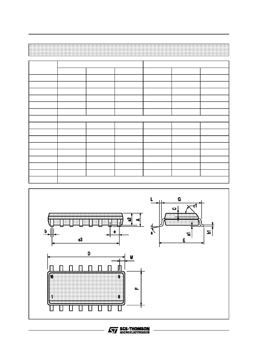
SO16 (Narrow) MECHANICAL DATA
DIM.
mm
inch
MIN.
TYP.
MAX.
MIN.
TYP.
MAX.
A
1.75
0.068
a1
0.1
0.2
0.004
0.007
a2
1.65
0.064
b
0.35
0.46
0.013
0.018
b1
0.19
0.25
0.007
0.010
C
0.5
0.019
c1
45
°
(typ.)
D
9.8
10
0.385
0.393
E
5.8
6.2
0.228
0.244
e
1.27
0.050
e3
8.89
0.350
F
3.8
4.0
0.149
0.157
G
4.6
5.3
0.181
0.208
L
0.5
1.27
0.019
0.050
M
0.62
0.024
S
8
°
(max.)
P013H
HCC/HCF4063B
10/12
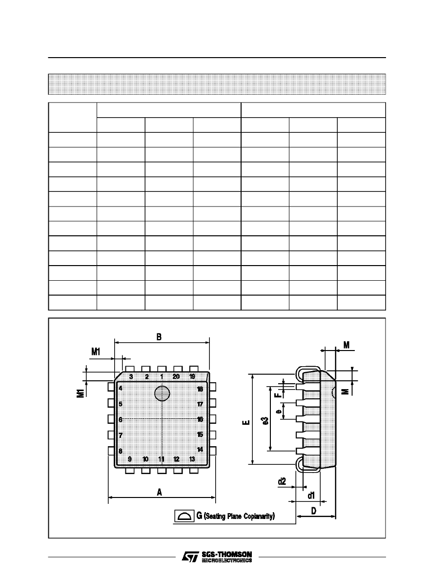
PLCC20 MECHANICAL DATA
DIM.
mm
inch
MIN.
TYP.
MAX.
MIN.
TYP.
MAX.
A
9.78
10.03
0.385
0.395
B
8.89
9.04
0.350
0.356
D
4.2
4.57
0.165
0.180
d1
2.54
0.100
d2
0.56
0.022
E
7.37
8.38
0.290
0.330
e
1.27
0.050
e3
5.08
0.200
F
0.38
0.015
G
0.101
0.004
M
1.27
0.050
M1
1.14
0.045
P027A
HCC/HCF4063B
11/12

Information furnished is believed to be accurate and reliable. However, SGS-THOMSON Microelectronics assumes no responsability for the
consequences of use of such information nor for any infringement of patents or other rights of third parties which may results from its use. No
license is granted by implication or otherwise under any patent or patent rights of SGS-THOMSON Microelectronics. Specifications mentioned
in this publication are subject to change without notice. This publication supersedes and replaces all information previously supplied.
SGS-THOMSON Microelectronics products are not authorized for use as critical components in life support devices or systems without express
written approval of SGS-THOMSON Microelectonics.
1994 SGS-THOMSON Microelectronics - All Rights Reserved
SGS-THOMSON Microelectronics GROUP OF COMPANIES
Australia - Brazil - France - Germany - Hong Kong - Italy - Japan - Korea - Malaysia - Malta - Morocco - The Netherlands -
Singapore - Spain - Sweden - Switzerland - Taiwan - Thailand - United Kingdom - U.S.A
HCC/HCF4063B
12/12
Wyszukiwarka
Podobne podstrony:
4063 ac
4063
4063 (Texas Instruments) id 384 Nieznany (2)
4063
4063
4063
4063
4063
4063
4063 ac
4063
4063 standstr ziemne2
4063
więcej podobnych podstron