1/17
March 2005
■
OUTPUT CURRENT UP TO 100 mA
■
OUTPUT VOLTAGES OF -5; -6; -8; -9; -12;
-15 V
■
THERMAL OVERLOAD PROTECTION
■
SHORT CIRCUIT PROTECTION
■
NO EXTERNAL COMPONENTS ARE
REQUIRED
■
AVAILABLE IN EITHER ± 5% (AC) OR ± 10%
(C) SELECTION
DESCRIPTION
The L79L00 series of three-terminal negative
regulators employ internal current limiting and
thermal shutdown, making them essentially
indestructible. If adequate heat-sink is provided,
they can deliver up to 100 mA output current.
They are intended as fixed voltage regulators in a
wide range of applications including local or
on-card regulation for elimination of noise and
distribution problems associated with single-point
regulation. In addition, they can be used with
power pass elements to make high-current
voltage regulators.
The L79L00 series used as Zener diode/resistor
combination replacement, offers an effective
output impedance improvement of typically two
orders of magnitude, along with lower quiescent
current and lower noise.
L79L00
SERIES
NEGATIVE VOLTAGE REGULATORS
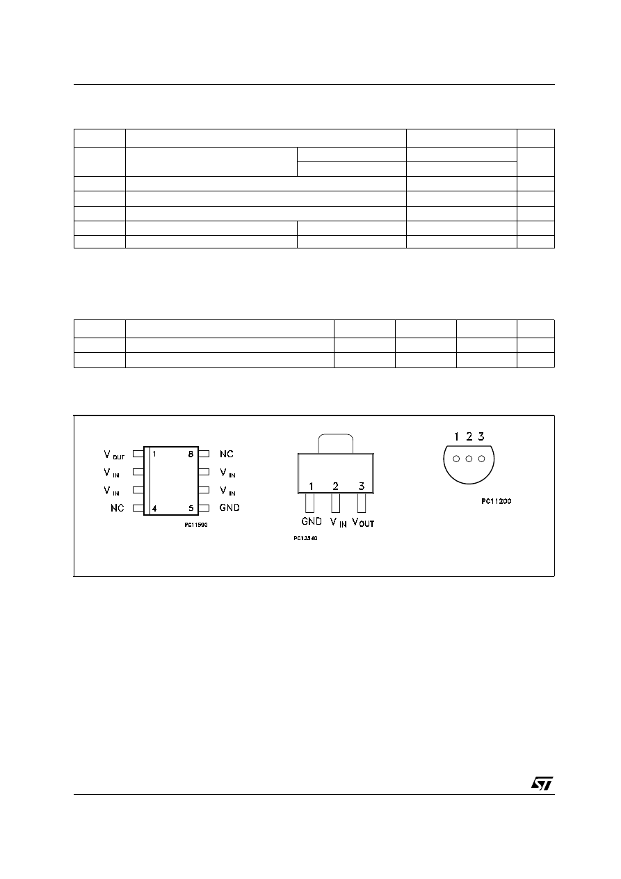
Figure 1: Schematic Diagram
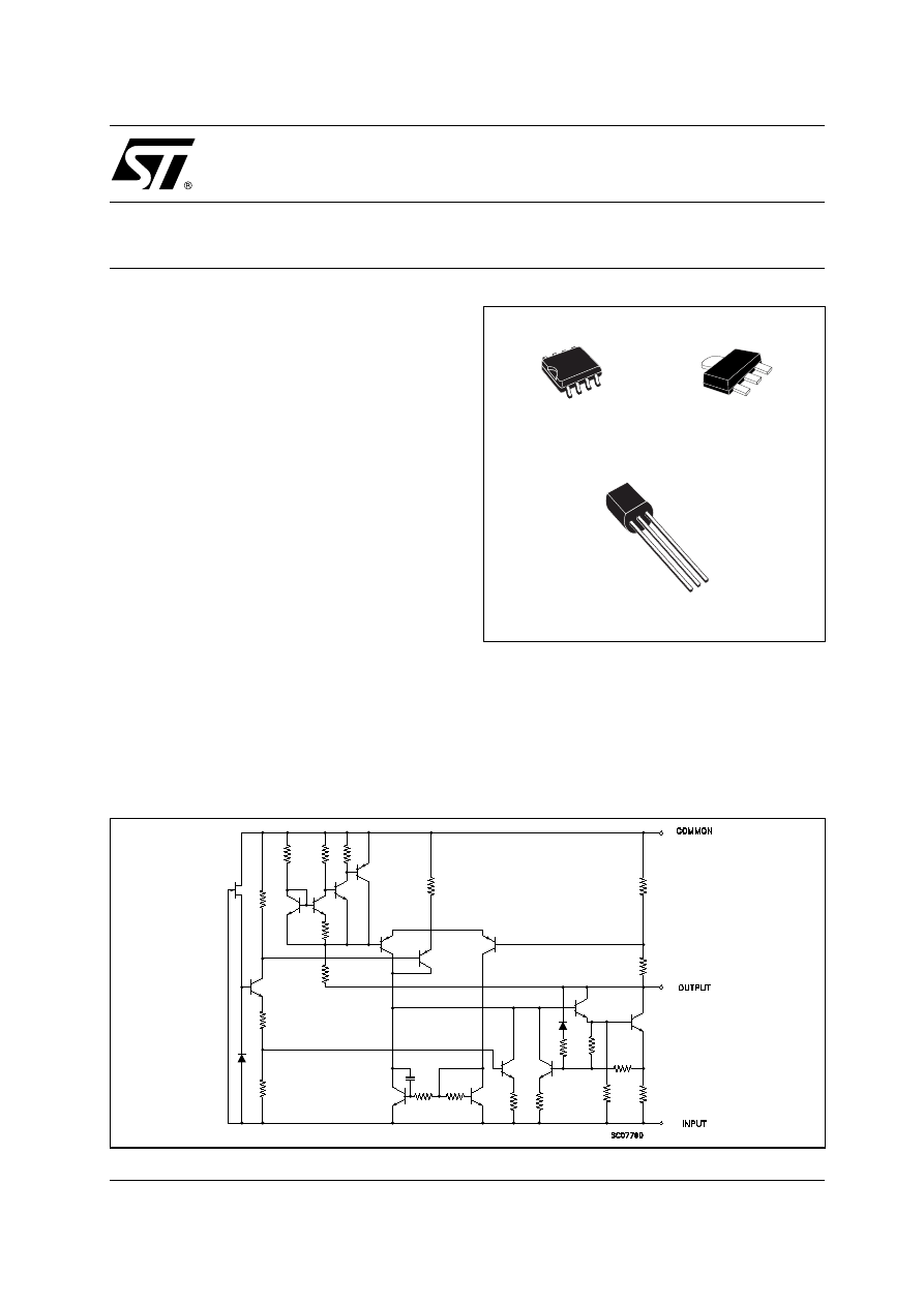
SO-8
SOT-89
TO-92
Rev. 10
L79L00 SERIES
2/17
Table 1: Absolute Maximum Ratings
(*) Our SO-8 package used for Voltage Regulators is modified internally to have pins 2, 3, 6 and 7 electrically communed to the die attach
flag. This particular frame decreases the total thermal resistance of the package and increases its ability to dissipate power when an appro-
priate area of copper on the printed circuit board is available for heat-sinking. The external dimensions are the same as for the standard SO-8.
Table 2: Thermal Data
(*) Considering 6 cm
2
of copper Board heat-sink.
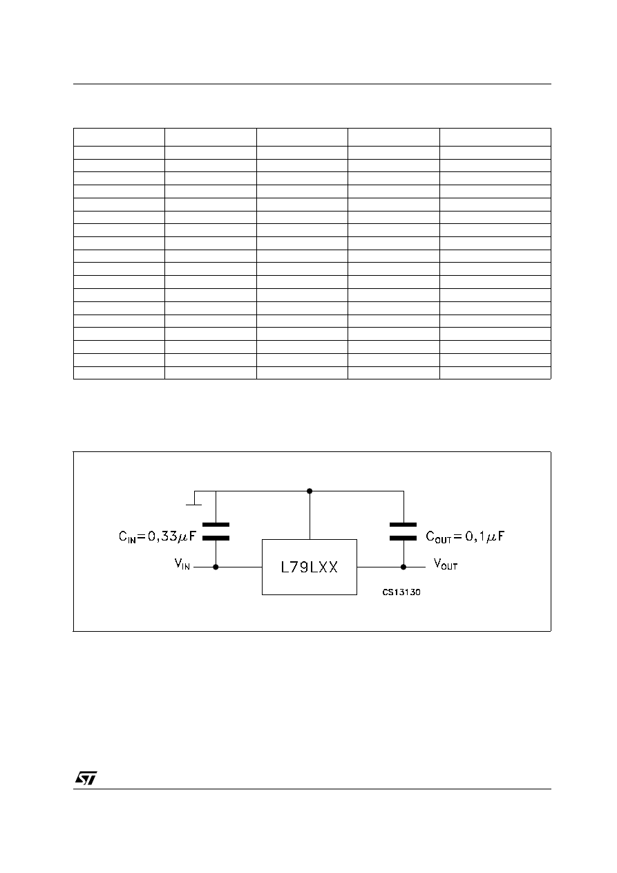
Figure 2: Pin Connection (top view, bottom view for TO-92)
Symbol
Parameter
Value
Unit
V
I
DC Input Voltage
V
O
= -5 to -9 V
-30
V
V
O
= -12 to -15 V
-35
I
O
Output Current
100
mA
P
tot
Power Dissipation
Internally Limited (*)
T
stg
Storage Temperature Range
-40 to 150
°C
T
op
Operating Junction Temperature Range
For L79L00C, L79L00AC
0 to 125
°C
For L79L00AB
-40 to 125
°C
Symbol
Parameter
SO-8
TO-92
SOT-89
Unit
R
thj-case
Thermal Resistance Junction-case Max
20
15
°C/W
R
thj-amb
Thermal Resistance Junction-ambient Max
55 (*)
200
°C/W
SO-8
TO-92
PIN 1 = GND
PIN 2 = V
IN
PIN 3 = V
OUT
SOT-89
L79L00 SERIES
3/17
Table 3: Order Codes
(*) Available in Tape & Reel with the suffix "13TR".
(**) Available in Ammopak with the suffix "-AP" or in Tape & Reel with the suffix "-TR". Please note that in these cases pins are shaped
according to Tape & Reel specifications.
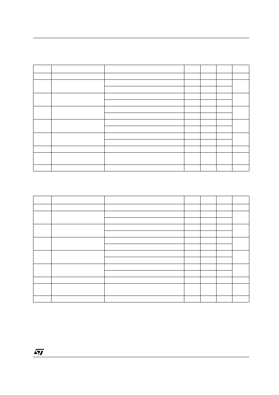
Figure 3: Test Circuits
TYPE
SO-8 (TUBE)*
TO-92 (TUBE)**
SOT-89 (T&R)
OUTPUT VOLTAGE
L79L05C
L79L05CD
L79L05CZ
-5 V
L79L05AC
L79L05ACD
L79L05ACZ
L79L05ACU
-5 V
L79L05AB
L79L05ABD
L79L05ABZ
L79L05ABU
-5 V
L79L06C
L79L06CD
L79L06CZ
-6 V
L79L06AC
L79L06ACD
L79L06ACZ
L79L06ACU
-6 V
L79L06AB
L79L06ABD
L79L06ABZ
L79L06ABU
-6 V
L79L08C
L79L08CD
L79L08CZ
-8 V
L79L08AC
L79L08ACD
L79L08ACZ
L79L08ACU
-8 V
L79L08AB
L79L08ABD
L79L08ABZ
L79L08ABU
-8 V
L79L09C
L79L09CD
L79L09CZ
-9 V
L79L09AC
L79L09ACD
L79L09ACZ
L79L09ACU
-9 V
L79L09AB
L79L09ABD
L79L09ABZ
L79L09ABU
-9 V
L79L12C
L79L12CD
L79L12CZ
-12 V
L79L12AC
L79L12ACD
L79L12ACZ
L79L12ACU
-12 V
L79L12AB
L79L12ABD
L79L12ABZ
L79L12ABU
-12 V
L79L15C
L79L15CD
L79L15CZ
-15 V
L79L15AC
L79L15ACD
L79L15ACZ
-15 V
L79L15AB
L79L15ABD
L79L15ABZ
-15 V

L79L00 SERIES
4/17
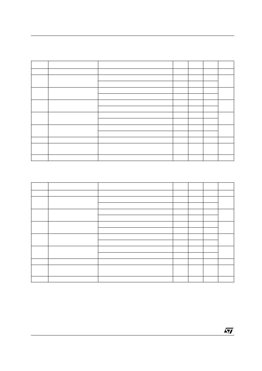
Table 4: Electrical Characteristics Of L79L05 (refer to the test circuits, T
J
= 0 to 125°C, V
I
= -10V,
I
O
= 40 mA, C
I
= 0.33 µF, C
O
= 0.1 µF unless otherwise specified).
Table 5: Electrical Characteristics Of L79L06 (refer to the test circuits, T
J
= 0 to 125°C, V
I
= -12V,
I
O
= 40 mA, C
I
= 0.33 µF, C
O
= 0.1 µF unless otherwise specified).
Symbol
Parameter
Test Conditions
Min.
Typ.
Max.
Unit
V
O
Output Voltage
T
J
= 25°C
-4.6
-5
-5.4
V
V
O
Output Voltage
I
O
= 1 to 40 mA
V
I
= -7 to -20 V
-4.5
-5.5
V
I
O
= 1 to 70 mA
V
I
= -10 V
-4.5
-5.5
∆
V
O
Line Regulation
V
I
= -7 to -20 V
T
J
= 25°C
200
mV
V
I
= -8 to -20 V
T
J
= 25°C
150
∆
V
O
Load Regulation
I
O
= 1 to 100 mA
T
J
= 25°C
60
mV
I
O
= 1 to 40 mA
T
J
= 25°C
30
I
d
Quiescent Current
T
J
= 25°C
6
mA
T
J
= 125°C
5.5
∆
I
d
Quiescent Current Change
I
O
= 1 to 40 mA
0.2
mA
V
I
= -8 to -20 V
1.5
eN
Output Noise Voltage
B = 10Hz to 100KHz
T
J
= 25°C
40
µ
V
SVR
Supply Voltage Rejection
I
O
= 40 mA f = 120Hz
T
J
= 25°C
V
I
= -8 to -18 V
40
49
dB
V
d
Dropout Voltage
1.7
V
Symbol
Parameter
Test Conditions
Min.
Typ.
Max.
Unit
V
O
Output Voltage
T
J
= 25°C
-5.52
-6
-6.48
V
V
O
Output Voltage
I
O
= 1 to 40 mA
V
I
= -8.5 to -20 V
-5.4
-6.6
V
I
O
= 1 to 70 mA
V
I
= -12 V
-5.4
-6.6
∆
V
O
Line Regulation
V
I
= -8.5 to -20 V
T
J
= 25°C
200
mV
V
I
= -9 to -20 V
T
J
= 25°C
150
∆
V
O
Load Regulation
I
O
= 1 to 100 mA
T
J
= 25°C
60
mV
I
O
= 1 to 40 mA
T
J
= 25°C
30
I
d
Quiescent Current
T
J
= 25°C
6
mA
T
J
= 125°C
5.5
∆
I
d
Quiescent Current Change
I
O
= 1 to 40 mA
0.2
mA
V
I
= -8 to -20 V
1.5
eN
Output Noise Voltage
B = 10Hz to 100KHz
T
J
= 25°C
50
µ
V
SVR
Supply Voltage Rejection
I
O
= 40 mA f = 120Hz
T
J
= 25°C
V
I
= -9 to -20 V
38
46
dB
V
d
Dropout Voltage
1.7
V
L79L00 SERIES
5/17
Table 6: Electrical Characteristics Of L79L08 (refer to the test circuits, T
J
= 0 to 125°C, V
I
= -14V,
I
O
= 40 mA, C
I
= 0.33 µF, C
O
= 0.1 µF unless otherwise specified).
Table 7: Electrical Characteristics Of L79L09 (refer to the test circuits, T
J
= 0 to 125°C, V
I
= -15V,
I
O
= 40 mA, C
I
= 0.33 µF, C
O
= 0.1 µF unless otherwise specified).
Symbol
Parameter
Test Conditions
Min.
Typ.
Max.
Unit
V
O
Output Voltage
T
J
= 25°C
-7.36
-8
-8.64
V
V
O
Output Voltage
I
O
= 1 to 40 mA
V
I
= -10.5 to -23 V
-7.2
-8.8
V
I
O
= 1 to 70 mA
V
I
= -14 V
-7.2
-8.8
∆
V
O
Line Regulation
V
I
= -10.5 to -23 V
T
J
= 25°C
200
mV
V
I
= -11 to -23 V
T
J
= 25°C
150
∆
V
O
Load Regulation
I
O
= 1 to 100 mA
T
J
= 25°C
80
mV
I
O
= 1 to 40 mA
T
J
= 25°C
40
I
d
Quiescent Current
T
J
= 25°C
6
mA
T
J
= 125°C
5.5
∆
I
d
Quiescent Current Change
I
O
= 1 to 40 mA
0.2
mA
V
I
= -11 to -23 V
1.5
eN
Output Noise Voltage
B = 10Hz to 100KHz
T
J
= 25°C
60
µ
V
SVR
Supply Voltage Rejection
I
O
= 40 mA f = 120Hz
T
J
= 25°C
V
I
= -12 to -23 V
36
45
dB
V
d
Dropout Voltage
1.7
V
Symbol
Parameter
Test Conditions
Min.
Typ.
Max.
Unit
V
O
Output Voltage
T
J
= 25°C
-8.28
-9
-9.72
V
V
O
Output Voltage
I
O
= 1 to 40 mA
V
I
= -11.5 to -23 V
-8.1
-9.9
V
I
O
= 1 to 70 mA
V
I
= -15 V
-8.1
-9.9
∆
V
O
Line Regulation
V
I
= -11.5 to -23 V
T
J
= 25°C
250
mV
V
I
= -12 to -23 V
T
J
= 25°C
200
∆
V
O
Load Regulation
I
O
= 1 to 100 mA
T
J
= 25°C
80
mV
I
O
= 1 to 40 mA
T
J
= 25°C
40
I
d
Quiescent Current
T
J
= 25°C
6
mA
T
J
= 125°C
5.5
∆
I
d
Quiescent Current Change
I
O
= 1 to 40 mA
0.2
mA
V
I
= -12 to -23 V
1.5
eN
Output Noise Voltage
B = 10Hz to 100KHz
T
J
= 25°C
70
µ
V
SVR
Supply Voltage Rejection
I
O
= 40 mA f = 120Hz
T
J
= 25°C
V
I
= -12 to -23 V
36
44
dB
V
d
Dropout Voltage
1.7
V
L79L00 SERIES
6/17
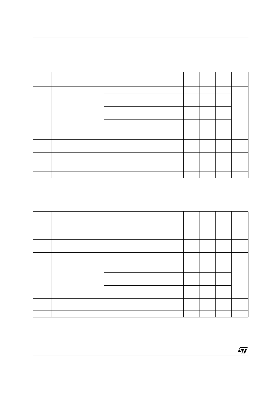
Table 8: Electrical Characteristics Of L79L12 (refer to the test circuits, T
J
= 0 to 125°C, V
I
= -19V,
I
O
= 40 mA, C
I
= 0.33 µF, C
O
= 0.1 µF unless otherwise specified).
Table 9: Electrical Characteristics Of L79L15 (refer to the test circuits, T
J
= 0 to 125°C, V
I
= -23V,
I
O
= 40 mA, C
I
= 0.33 µF, C
O
= 0.1 µF unless otherwise specified).
Symbol
Parameter
Test Conditions
Min.
Typ.
Max.
Unit
V
O
Output Voltage
T
J
= 25°C
-11.1
-12
-12.9
V
V
O
Output Voltage
I
O
= 1 to 40 mA
V
I
= -14.5 to -27 V
-10.8
-13.2
V
I
O
= 1 to 70 mA
V
I
= -19 V
-10.8
-13.2
∆
V
O
Line Regulation
V
I
= -14.5 to -27 V
T
J
= 25°C
250
mV
V
I
= -16 to -27 V
T
J
= 25°C
200
∆
V
O
Load Regulation
I
O
= 1 to 100 mA
T
J
= 25°C
100
mV
I
O
= 1 to 40 mA
T
J
= 25°C
50
I
d
Quiescent Current
T
J
= 25°C
6.5
mA
T
J
= 125°C
6
∆
I
d
Quiescent Current Change
I
O
= 1 to 40 mA
0.2
mA
V
I
= -16 to -27 V
1.5
eN
Output Noise Voltage
B = 10Hz to 100KHz
T
J
= 25°C
80
µ
V
SVR
Supply Voltage Rejection
I
O
= 40 mA f = 120Hz
T
J
= 25°C
V
I
= -15 to -25 V
36
42
dB
V
d
Dropout Voltage
1.7
V
Symbol
Parameter
Test Conditions
Min.
Typ.
Max.
Unit
V
O
Output Voltage
T
J
= 25°C
-13.8
-15
-16.2
V
V
O
Output Voltage
I
O
= 1 to 40 mA
V
I
= -17.5 to -30 V
-13.5
-16.5
V
I
O
= 1 to 70 mA
V
I
= -23 V
-13.5
-16.5
∆
V
O
Line Regulation
V
I
= -17.5 to -30 V
T
J
= 25°C
300
mV
V
I
= -20 to -30 V
T
J
= 25°C
250
∆
V
O
Load Regulation
I
O
= 1 to 100 mA
T
J
= 25°C
150
mV
I
O
= 1 to 40 mA
T
J
= 25°C
75
I
d
Quiescent Current
T
J
= 25°C
6.5
mA
T
J
= 125°C
6
∆
I
d
Quiescent Current Change
I
O
= 1 to 40 mA
0.2
mA
V
I
= -20 to -30 V
1.5
eN
Output Noise Voltage
B = 10Hz to 100KHz
T
J
= 25°C
90
µ
V
SVR
Supply Voltage Rejection
I
O
= 40 mA f = 120Hz
T
J
= 25°C
V
I
= -18.5 to -28.5 V
33
39
dB
V
d
Dropout Voltage
1.7
V
L79L00 SERIES
7/17
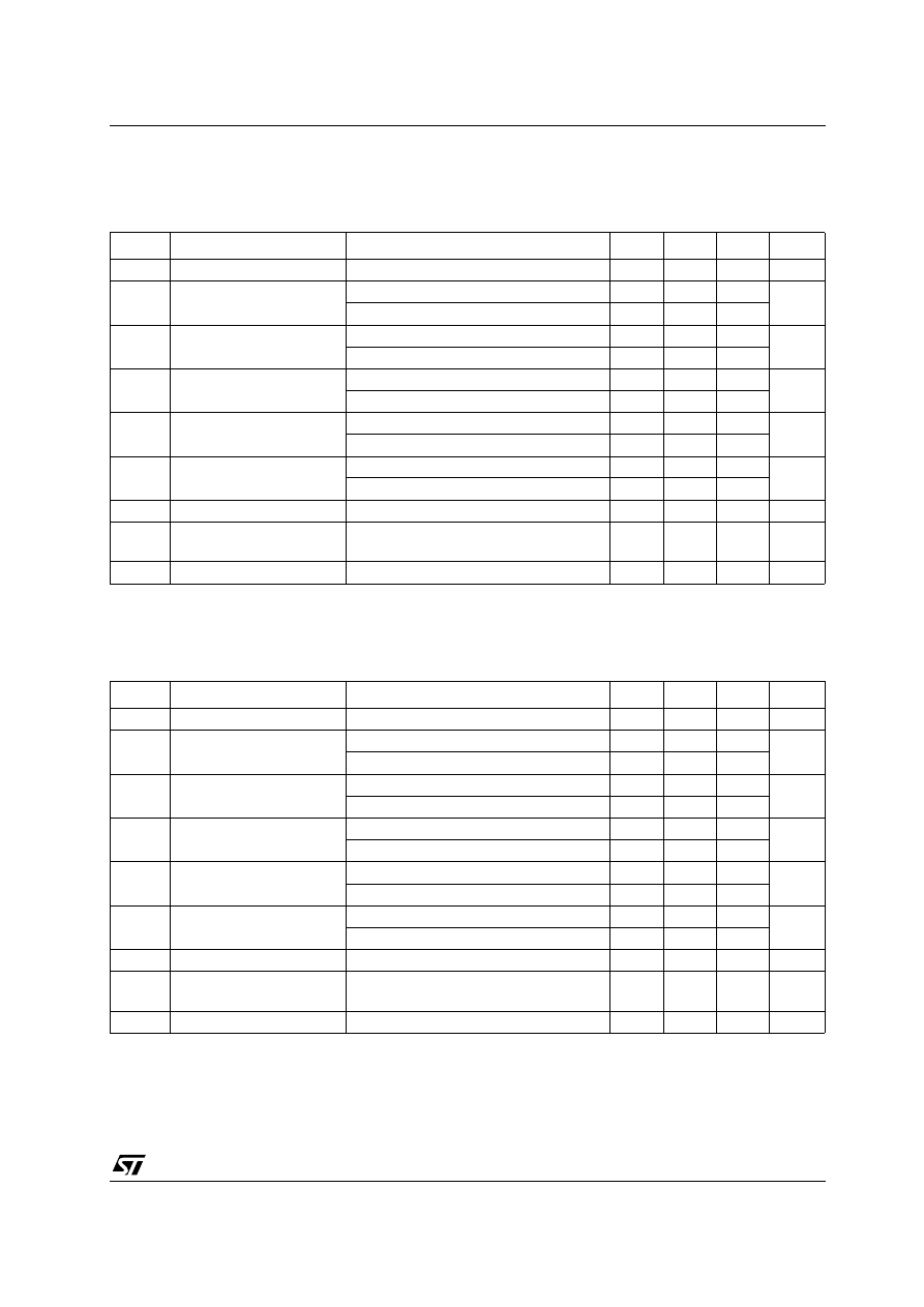
Table 10: Electrical Characteristics Of L79L05AB And L79L05AC (refer to the test circuits, V
I
= -10V,
I
O
= 40 mA, C
I
= 0.33 µF, C
O
= 0.1 µF, T
J
= 0 to 125°C for L79L05AC, T
J
= -40 to 125°C for L79L05AB,
unless otherwise specified).
Table 11: Electrical Characteristics Of L79L06AB And L79L06AC (refer to the test circuits, V
I
= -12V,
I
O
= 40 mA, C
I
= 0.33 µF, C
O
= 0.1 µF, T
J
= 0 to 125°C for L79L06AC, T
J
= -40 to 125°C for L79L06AB,
unless otherwise specified).
Symbol
Parameter
Test Conditions
Min.
Typ.
Max.
Unit
V
O
Output Voltage
T
J
= 25°C
-4.8
-5
-5.2
V
V
O
Output Voltage
I
O
= 1 to 40 mA
V
I
= -7 to -20 V
-4.75
-5.25
V
I
O
= 1 to 70 mA
V
I
= -10 V
-4.75
-5.25
∆
V
O
Line Regulation
V
I
= -7 to -20 V
T
J
= 25°C
150
mV
V
I
= -8 to -20 V
T
J
= 25°C
100
∆
V
O
Load Regulation
I
O
= 1 to 100 mA
T
J
= 25°C
60
mV
I
O
= 1 to 40 mA
T
J
= 25°C
30
I
d
Quiescent Current
T
J
= 25°C
6
mA
T
J
= 125°C
5.5
∆
I
d
Quiescent Current Change
I
O
= 1 to 40 mA
0.1
mA
V
I
= -8 to -20 V
1.5
eN
Output Noise Voltage
B = 10Hz to 100KHz
T
J
= 25°C
40
µ
V
SVR
Supply Voltage Rejection
I
O
= 40 mA f = 120Hz
T
J
= 25°C
V
I
= -8 to -18 V
41
49
dB
V
d
Dropout Voltage
1.7
V
Symbol
Parameter
Test Conditions
Min.
Typ.
Max.
Unit
V
O
Output Voltage
T
J
= 25°C
-5.76
-6
-6.24
V
V
O
Output Voltage
I
O
= 1 to 40 mA
V
I
= -8.5 to -20 V
-5.7
-6.3
V
I
O
= 1 to 70 mA
V
I
= -12 V
-5.7
-6.3
∆
V
O
Line Regulation
V
I
= -8.5 to -20 V
T
J
= 25°C
150
mV
V
I
= -9 to -20 V
T
J
= 25°C
100
∆
V
O
Load Regulation
I
O
= 1 to 100 mA
T
J
= 25°C
60
mV
I
O
= 1 to 40 mA
T
J
= 25°C
30
I
d
Quiescent Current
T
J
= 25°C
6
mA
T
J
= 125°C
5.5
∆
I
d
Quiescent Current Change
I
O
= 1 to 40 mA
0.1
mA
V
I
= -9 to -20 V
1.5
eN
Output Noise Voltage
B = 10Hz to 100KHz
T
J
= 25°C
50
µ
V
SVR
Supply Voltage Rejection
I
O
= 40 mA f = 120Hz
T
J
= 25°C
V
I
= -9 to -20 V
39
46
dB
V
d
Dropout Voltage
1.7
V
L79L00 SERIES
8/17
Table 12: Electrical Characteristics Of L79L08AB And L79L08AC (refer to the test circuits, V
I
= -14V,
I
O
= 40 mA, C
I
= 0.33 µF, C
O
= 0.1 µF, T
J
= 0 to 125°C for L79L08AC, T
J
= -40 to 125°C for L79L08AB,
unless otherwise specified).
Table 13: Electrical Characteristics Of L79L09AB And L79L09AC (refer to the test circuits, V
I
= -15V,
I
O
= 40 mA, C
I
= 0.33 µF, C
O
= 0.1 µF, T
J
= 0 to 125°C for L79L09AC, T
J
= -40 to 125°C for L79L09AB,
unless otherwise specified).
Symbol
Parameter
Test Conditions
Min.
Typ.
Max.
Unit
V
O
Output Voltage
T
J
= 25°C
-7.68
-8
-8.32
V
V
O
Output Voltage
I
O
= 1 to 40 mA
V
I
= -10.5 to -23 V
-7.6
-8.4
V
I
O
= 1 to 70 mA
V
I
= -14 V
-7.6
-8.4
∆
V
O
Line Regulation
V
I
= -10.5 to -23 V
T
J
= 25°C
175
mV
V
I
= -11 to -23 V
T
J
= 25°C
125
∆
V
O
Load Regulation
I
O
= 1 to 100 mA
T
J
= 25°C
80
mV
I
O
= 1 to 40 mA
T
J
= 25°C
40
I
d
Quiescent Current
T
J
= 25°C
6
mA
T
J
= 125°C
5.5
∆
I
d
Quiescent Current Change
I
O
= 1 to 40 mA
0.1
mA
V
I
= -11 to -23 V
1.5
eN
Output Noise Voltage
B = 10Hz to 100KHz
T
J
= 25°C
60
µ
V
SVR
Supply Voltage Rejection
I
O
= 40 mA f = 120Hz
T
J
= 25°C
V
I
= -12 to -23 V
37
45
dB
V
d
Dropout Voltage
1.7
V
Symbol
Parameter
Test Conditions
Min.
Typ.
Max.
Unit
V
O
Output Voltage
T
J
= 25°C
-8.64
-9
-9.36
V
V
O
Output Voltage
I
O
= 1 to 40 mA
V
I
= -11.5 to -23 V
-8.55
-9.45
V
I
O
= 1 to 70 mA
V
I
= -15 V
-8.55
-9.45
∆
V
O
Line Regulation
V
I
= -11.5 to -23 V
T
J
= 25°C
225
mV
V
I
= -12 to -23 V
T
J
= 25°C
150
∆
V
O
Load Regulation
I
O
= 1 to 100 mA
T
J
= 25°C
80
mV
I
O
= 1 to 40 mA
T
J
= 25°C
40
I
d
Quiescent Current
T
J
= 25°C
6
mA
T
J
= 125°C
5.5
∆
I
d
Quiescent Current Change
I
O
= 1 to 40 mA
0.1
mA
V
I
= -12 to -23 V
1.5
eN
Output Noise Voltage
B = 10Hz to 100KHz
T
J
= 25°C
70
µ
V
SVR
Supply Voltage Rejection
I
O
= 40 mA f = 120Hz
T
J
= 25°C
V
I
= -12 to -23 V
37
44
dB
V
d
Dropout Voltage
1.7
V
L79L00 SERIES
9/17
Table 14: Electrical Characteristics Of L79L12AB And L79L12AC (refer to the test circuits, V
I
= -19V,
I
O
= 40 mA, C
I
= 0.33 µF, C
O
= 0.1 µF, T
J
= 0 to 125°C for L79L12AC, T
J
= -40 to 125°C for L79L12AB,
unless otherwise specified).
Figure 4: Electrical Characteristics Of L79L15AB And L79L15AC (refer to the test circuits, V
I
= -23V,
I
O
= 40 mA, C
I
= 0.33 µF, C
O
= 0.1 µF, T
J
= 0 to 125°C for L79L15AC, T
J
= -40 to 125°C for L79L15AB,
unless otherwise specified).
Symbol
Parameter
Test Conditions
Min.
Typ.
Max.
Unit
V
O
Output Voltage
T
J
= 25°C
-11.5
-12
-12.5
V
V
O
Output Voltage
I
O
= 1 to 40 mA
V
I
= -14.5 to -27 V
-11.4
-12.6
V
I
O
= 1 to 70 mA
V
I
= -19 V
-11.4
-12.6
∆
V
O
Line Regulation
V
I
= -14.5 to -27 V
T
J
= 25°C
250
mV
V
I
= -16 to -27 V
T
J
= 25°C
200
∆
V
O
Load Regulation
I
O
= 1 to 100 mA
T
J
= 25°C
100
mV
I
O
= 1 to 40 mA
T
J
= 25°C
50
I
d
Quiescent Current
T
J
= 25°C
6.5
mA
T
J
= 125°C
6
∆
I
d
Quiescent Current Change
I
O
= 1 to 40 mA
0.1
mA
V
I
= -16 to -27 V
1.5
eN
Output Noise Voltage
B = 10Hz to 100KHz
T
J
= 25°C
80
µ
V
SVR
Supply Voltage Rejection
I
O
= 40 mA f = 120Hz
T
J
= 25°C
V
I
= -15 to -25 V
37
42
dB
V
d
Dropout Voltage
1.7
V
Symbol
Parameter
Test Conditions
Min.
Typ.
Max.
Unit
V
O
Output Voltage
T
J
= 25°C
-14.4
-15
-15.6
V
V
O
Output Voltage
I
O
= 1 to 40 mA
V
I
= -17.5 to -30 V
-14.25
-15.75
V
I
O
= 1 to 70 mA
V
I
= -23 V
-14.25
-15.75
∆
V
O
Line Regulation
V
I
= -17.5 to -30 V
T
J
= 25°C
300
mV
V
I
= -20 to -30 V
T
J
= 25°C
250
∆
V
O
Load Regulation
I
O
= 1 to 100 mA
T
J
= 25°C
150
mV
I
O
= 1 to 40 mA
T
J
= 25°C
75
I
d
Quiescent Current
T
J
= 25°C
6.5
mA
T
J
= 125°C
6
∆
I
d
Quiescent Current Change
I
O
= 1 to 40 mA
0.1
mA
V
I
= -20 to -30 V
1.5
eN
Output Noise Voltage
B = 10Hz to 100KHz
T
J
= 25°C
90
µ
V
SVR
Supply Voltage Rejection
I
O
= 40 mA f = 120Hz
T
J
= 25°C
V
I
= -18.5 to -28.5 V
34
39
dB
V
d
Dropout Voltage
1.7
V
L79L00 SERIES
10/17
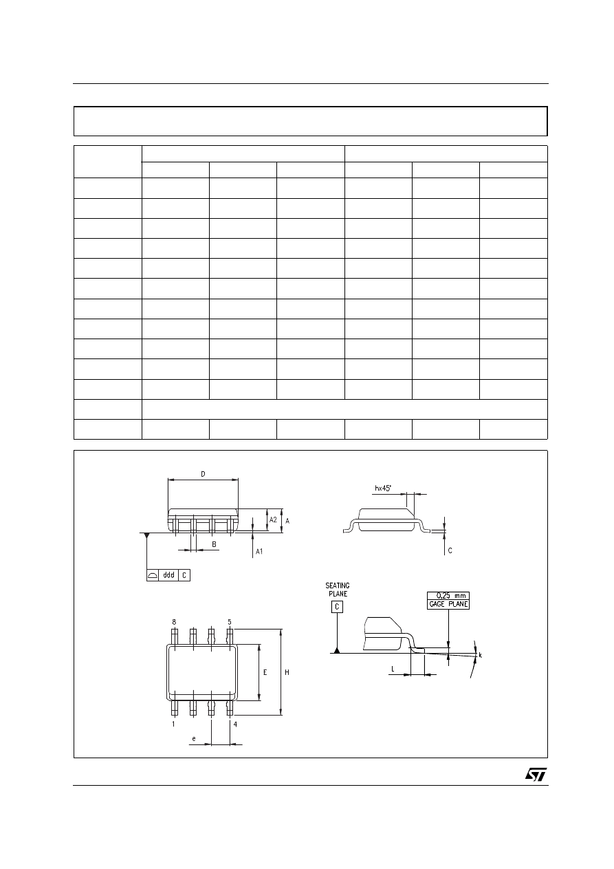
DIM.
mm.
inch
MIN.
TYP
MAX.
MIN.
TYP.
MAX.
A
1.35
1.75
0.053
0.069
A1
0.10
0.25
0.04
0.010
A2
1.10
1.65
0.043
0.065
B
0.33
0.51
0.013
0.020
C
0.19
0.25
0.007
0.010
D
4.80
5.00
0.189
0.197
E
3.80
4.00
0.150
0.157
e
1.27
0.050
H
5.80
6.20
0.228
0.244
h
0.25
0.50
0.010
0.020
L
0.40
1.27
0.016
0.050
k
˚ (max.)
ddd
0.1
0.04
SO-8 MECHANICAL DATA
0016023/C
8
L79L00 SERIES
11/17
DIM.
mm.
mils
MIN.
TYP
MAX.
MIN.
TYP.
MAX.
A
1.4
1.6
55.1
63.0
B
0.44
0.56
17.3
22.0
B1
0.36
0.48
14.2
18.9
C
0.35
0.44
13.8
17.3
C1
0.35
0.44
13.8
17.3
D
4.4
4.6
173.2
181.1
D1
1.62
1.83
63.8
72.0
E
2.29
2.6
90.2
102.4
e
1.42
1.57
55.9
61.8
e1
2.92
3.07
115.0
120.9
H
3.94
4.25
155.1
167.3
L
0.89
1.2
35.0
47.2
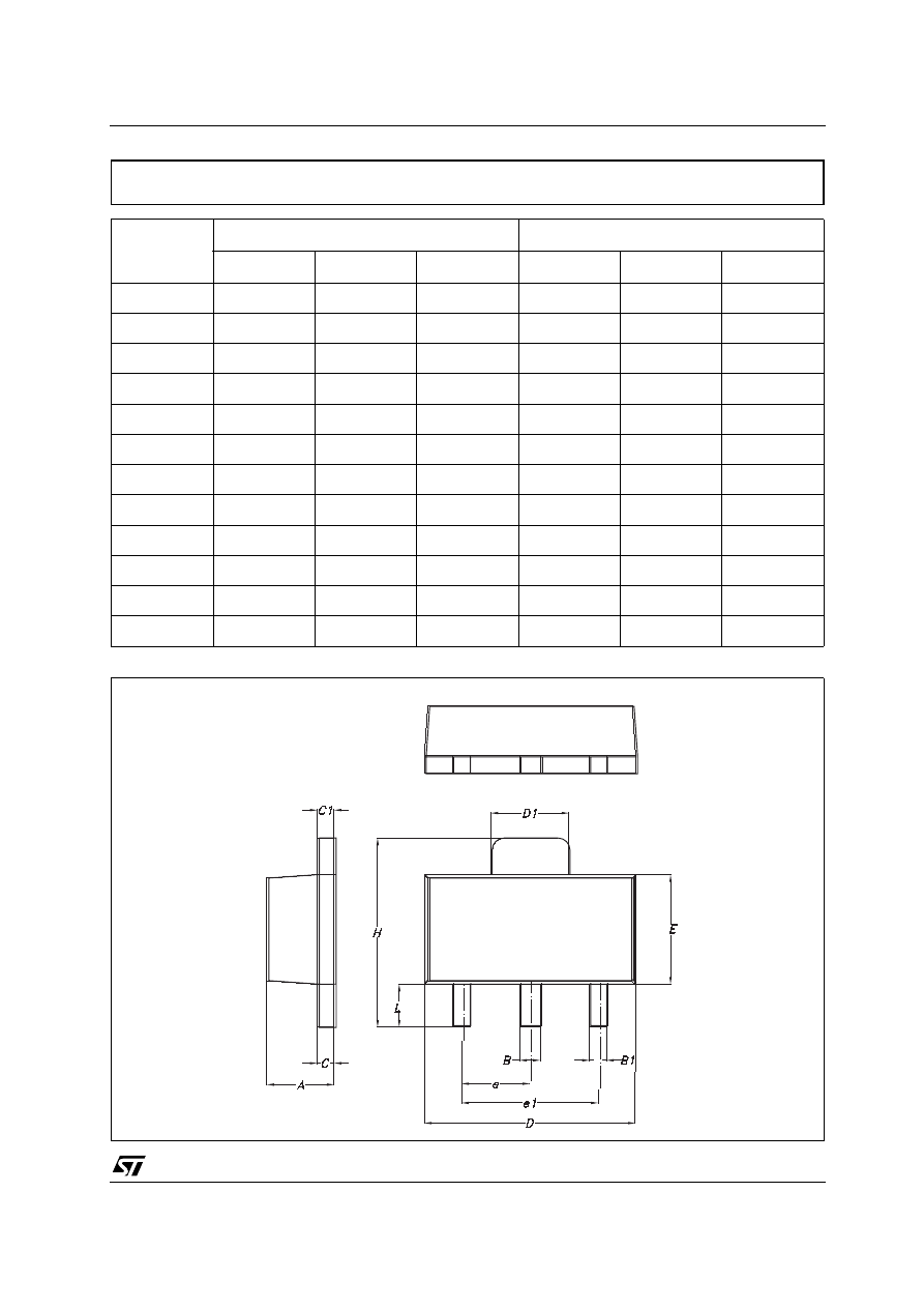
SOT-89 MECHANICAL DATA
P025H
L79L00 SERIES
12/17
DIM.
mm.
mils
MIN.
TYP
MAX.
MIN.
TYP.
MAX.
A
4.32
4.95
170.1
194.9
b
0.36
0.51
14.2
20.1
D
4.45
4.95
175.2
194.9
E
3.30
3.94
129.9
155.1
e
2.41
2.67
94.9
105.1
e1
1.14
1.40
44.9
55.1
L
12.7
15.49
500.0
609.8
R
2.16
2.41
85.0
94.9
S1
0.92
1.52
36.2
59.8
W
0.41
0.56
16.1
22.0
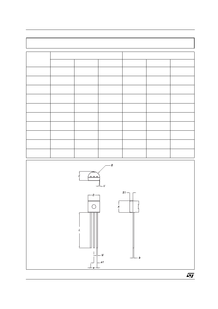
TO-92 MECHANICA DATA
0102782/C
L79L00 SERIES
13/17
DIM.
mm.
inch
MIN.
TYP
MAX.
MIN.
TYP.
MAX.
A
330
12.992
C
12.8
13.2
0.504
0.519
D
20.2
0.795
N
60
2.362
T
22.4
0.882
Ao
8.1
8.5
0.319
0.335
Bo
5.5
5.9
0.216
0.232
Ko
2.1
2.3
0.082
0.090
Po
3.9
4.1
0.153
0.161
P
7.9
8.1
0.311
0.319
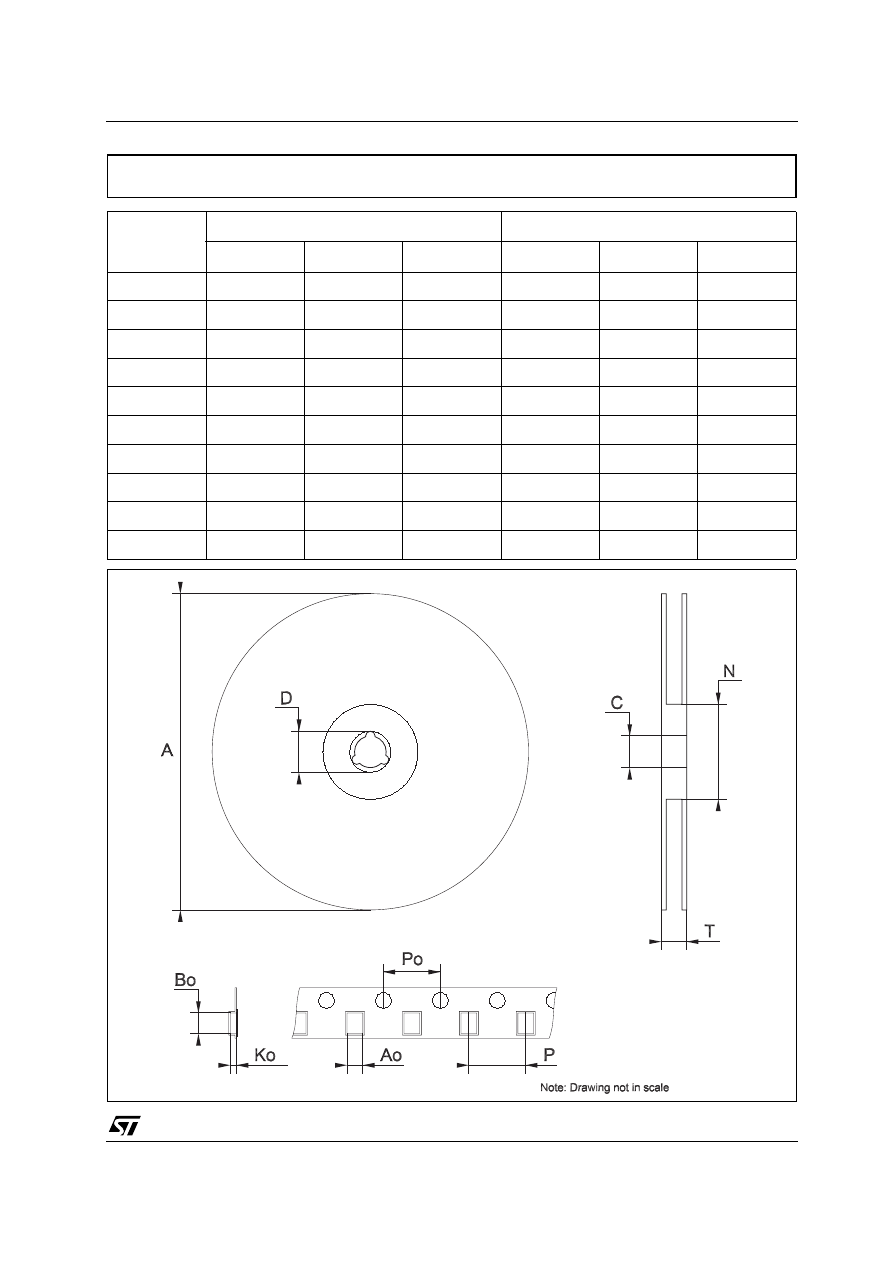
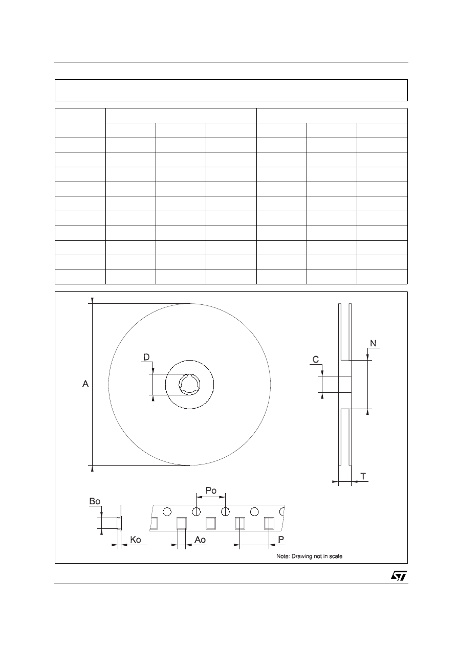
Tape & Reel SO-8 MECHANICAL DATA
L79L00 SERIES
14/17
DIM.
mm.
inch
MIN.
TYP
MAX.
MIN.
TYP.
MAX.
A
180
7.086
C
12.8
13.0
13.2
0.504
0.512
0.519
D
20.2
0.795
N
60
2.362
T
14.4
0.567
Ao
4.70
4.80
4.90
0.185
0.189
0.193
Bo
4.30
4.40
4.50
0.169
0.173
0.177
Ko
1.70
1.80
1.90
0.067
0.071
0.075
Po
3.9
4.0
4.1
0.153
0.157
0.161
P
7.9
8.0
8.1
0.311
0.315
0.319
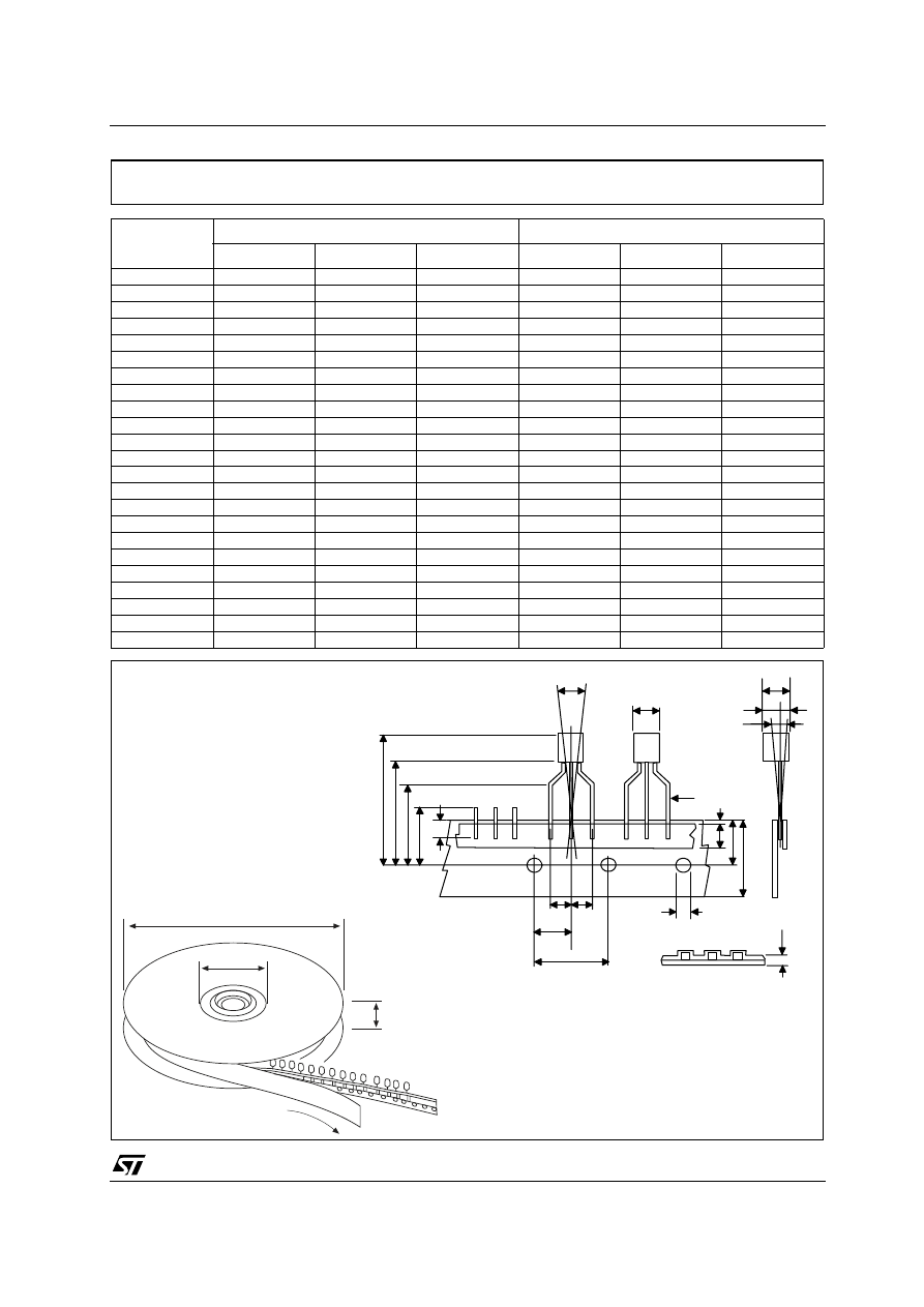
Tape & Reel SOT89 MECHANICAL DATA
L79L00 SERIES
15/17
DIM.
mm.
inch
MIN.
TYP
MAX.
MIN.
TYP.
MAX.
A1
4.80
0.189
T
3.80
0.150
T1
1.60
0.063
T2
2.30
0.091
d
0.48
0.019
P0
12.5
12.9
0.492
0.508
P2
5.65
7.05
0.222
0.278
F1, F2
2.44
2.54
2.94
0.096
0.100
0.116
delta H
±2
0.079
W
17.5
18.00
19.0
0.689
0.709
0.748
W0
5.7
6.3
0.224
0.248
W1
8.5
9.25
0.335
0.364
W2
0.50
0.20
H
18.50
18.70
0.728
0.726
H0
15.50
16.50
0.610
0.650
H1
25.00
0.984
D0
3.8
4.2
0.150
0.165
t
0.90
0.035
L1
3
0.118
delta P
±1
0.039
u
50
1.968
Φ
1
360
14.173
Φ
2
30
1.181
Tape & Reel for TO-92 MECHANICAL DATA
Φ
1
Φ
2
u
Pull-out direction
W
W1
W0
W2
A1
d
D0
H1
H
H0
L
l1
F1 F2
P2
P0
delta P
delta H
T2
T1
T
t
DRAWING NOT IN SCALE
L79L00 SERIES
16/17
Table 15: Revision History
Date
Revision
Description of Changes
14-Mar-2005
9
Add Tape & Reel for TO-92.
15-Mar-2005
10
Add note on Table 3.

L79L00 SERIES
17/17
Information furnished is believed to be accurate and reliable. However, STMicroelectronics assumes no responsibility for the consequences
of use of such information nor for any infringement of patents or other rights of third parties which may result from its use. No license is granted
by implication or otherwise under any patent or patent rights of STMicroelectronics. Specifications mentioned in this publication are subject
to change without notice. This publication supersedes and replaces all information previously supplied. STMicroelectronics products are not
authorized for use as critical components in life support devices or systems without express written approval of STMicroelectronics.
The ST logo is a registered trademark of STMicroelectronics
All other names are the property of their respective owners
© 2005 STMicroelectronics - All Rights Reserved
STMicroelectronics group of companies
Australia - Belgium - Brazil - Canada - China - Czech Republic - Finland - France - Germany - Hong Kong - India - Israel - Italy - Japan -
Malaysia - Malta - Morocco - Singapore - Spain - Sweden - Switzerland - United Kingdom - United States of America
www.st.com
Document Outline
- Figure 1: Schematic Diagram
- Table 1: Absolute Maximum Ratings
- Table 2: Thermal Data
- Figure 2: Pin Connection (top view, bottom view for TO-92)
- Table 3: Order Codes
- Figure 3: Test Circuits
- Table 4: Electrical Characteristics Of L79L05 (refer to the test circuits, TJ = 0 to 125˚C, VI = ...
- Table 5: Electrical Characteristics Of L79L06 (refer to the test circuits, TJ = 0 to 125˚C, VI = ...
- Table 6: Electrical Characteristics Of L79L08 (refer to the test circuits, TJ = 0 to 125˚C, VI = ...
- Table 7: Electrical Characteristics Of L79L09 (refer to the test circuits, TJ = 0 to 125˚C, VI = ...
- Table 8: Electrical Characteristics Of L79L12 (refer to the test circuits, TJ = 0 to 125˚C, VI = ...
- Table 9: Electrical Characteristics Of L79L15 (refer to the test circuits, TJ = 0 to 125˚C, VI = ...
- Table 10: Electrical Characteristics Of L79L05AB And L79L05AC (refer to the test circuits, VI = -...
- Table 11: Electrical Characteristics Of L79L06AB And L79L06AC (refer to the test circuits, VI = -...
- Table 12: Electrical Characteristics Of L79L08AB And L79L08AC (refer to the test circuits, VI = -...
- Table 13: Electrical Characteristics Of L79L09AB And L79L09AC (refer to the test circuits, VI = -...
- Table 14: Electrical Characteristics Of L79L12AB And L79L12AC (refer to the test circuits, VI = -...
- Figure 4: Electrical Characteristics Of L79L15AB And L79L15AC (refer to the test circuits, VI = -...
- Table 15: Revision History
Wyszukiwarka
Podobne podstrony:
2511
2511
2511
Anne Mather An All Consuming Passion [HP 899, MB 2511] (docx)
więcej podobnych podstron