
1/14
Basics of Electronics
Design Project no 1^8 2a
Polish Japanese Institute of Technology 2006
2/14
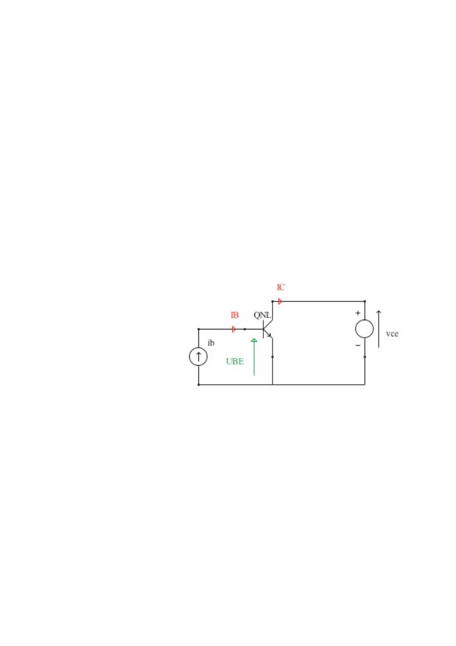
Task 1. Transistor Investigation
Using Pspice simulator plot the static output and input
characteristics of the 2n3904 transistor for the common emitter
circuit with the emitter area increased 0.61 times. Plot the I
C
and I
B
currents as a funciton of the base-emitter voltage U
BE
for large
change of the currents. Draw all plots for the junction temperatures
32
o
C and 52
o
C. Discuss the influence of the temperature to the plots.
Assignment attachments: zad1.cir, zad1.out.
Zad1.cir holds the data for all the measurments in this task. The
netlist contains two sources:
the vce voltage source that constitutes the difference of potentials
between the collector and emitter nodes of the q1 transistor. It’s value has
been set at the Q-point collector-emitter voltage in task 2 for
convenience.
the ib current source that constitutes the current flowing in the base node.
It’s value has been set
by the Q-point value
of the collector current
in task 2 for
convenience.
the q1 is the
investigated transistor.
The zad1.cir
contains two .dc
declarations for the
base current sweep
and collector-emitter
voltage sweep, each, depending on the nature of the analysis, has been
subsequently commented out.
I have copied the list of properties of the QNL transistor from the
2N3904 transistor model from the eval.lib file provided with Pspice
Evaluation 6.1.
The measurements have been made for the temperatures 32 and 52
degrees as well as the temperature 27 degrees for further use.
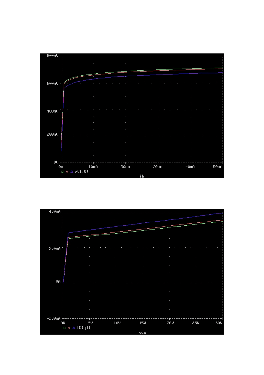
The static input characteristic is the relation of the base-emitter
voltage to the base current whilst the collector-emitter voltage is a
constant, in our case – 6V. For the investigated transistor the dependency
is as in the graph below.
Diagram 1-1
3/14
The base-emitter voltage has been estimated as the difference of
potentials between node 1 and
0.
The transistor’s output characteristic is the relation of the collector
current to the collector-emitter voltage whilst the base current is a
constant (hereby at 15
uA).

4/14
Legend: – 27
o
C, – 32
o
C, – 52
o
C.
Both the input and output characteristics are of the logarithmic rank
and obviously depend on the junction temperature. That is to be
anticipated, given the following dependency:
!
I
C
= I
s
(e
V
BE
(kT / q )
"1)
where (kT/q) is the voltage equivalent temperature, q is the electron
charge, k is the Boltzmann constant, I
S
is the saturation current and T is
the transistor’s temperature, so the influence of the transistor‘s
temperature on it’s output characteristic is apparent.

5/14
Task 2. Amplifier Investigation – part 1
Design the amplifier using the 2n3904 transistor in the common
emitter circuit with the divider in the base circuit and feedback in the
emitter circuit. The frequency range of the amplifier: f
L
= 22 Hz, f
H
=
32 kHz (-3dB). Calculate all resistors and capacitors, the current and
voltage amplification factors k
i
and k
u
, input and output impedances
and the maximum output amplitude. Use the source and load
resistances R
S
= 22 k
Ω
and R
L
= 32 k
Ω
respectively. For all hand
calculations use the simple transistor equivalent circuit r
bb‘
= 0 and
h
22
= 0. Please make all calculations for the junction temperature t
j1
=
27
o
C and supply voltage E
CC
= 22 V. Calculate the change of the
transistor operating point and the change of all dynamic data of the
amplifier when the junction temperature changes to tj2 = 52
o
C.
The prologue:
A BJT amplifier with a single transistor working in the common
emitter arrangement is used to amplify signals with small amplitudes in
the small frequency range. One of it’s most common applications is
acoustics (such as sound wave to electric signal conversion in
microphones). Such a circuit reverses the input signal’s phase, has good
parameters, a simple construction and is easy to procure. It’s active
element is a BJT transistor, hence the name. All the passive elements of
the circuit (resistors and capacitors) provide the neccesary conditions.
The schematic for this project’s BJT amplifier is to be found in Task 3.
Step-by-step guidelines:
1. Choice of the operating point and calculating R
C
and R
E
.
2. Calculating R
1
, R
2
and R
B
.
3. Calculating C
1
, C
C
and C
E
.
4. Calculating the f
H
, R
IN
, R
OUT
, k
v
, k
i
.
5. Performing any necessary circuit modifications before proceeding to
task 3.
Calculations:
6/14
On the basis of the calculations done in Pspice in the course of the
first task I will assume the operating point coordinates such that they, I
estimate, should assure reasonable compromise for the best temperature
behavior, maximum voltage gain and maximum output amplitude:
V
CEQ
=
3
8
V
CC
V
CEQ
= 8.25V
I
CQ
= 2.7mA
Henceforth:
V
outMax( )
= V
CEQ
V
CES
, where the saturation voltage V
CES
=1V according to the
Pspice readout from task 1, so:
!
V
outMax(")
= 8)25V "1V = 7)25V
Given that for an undistorted output signal we need for
V
outMax(+)
= V
outMax( )
= V
outMax
= 7.25V
and given that
!
V
outMax
= I
CQ
(R
C
R
L
)
R
C
=
V
outMax
R
L
I
CQ
R
L
V
outMax
, where
!
R
L
= 32k"
R
C
= 2.931k
Given the equation:
!
E
C
+ E
E
=
V
CC
" V
CEQ
I
CQ
, so for the given operating point:
!
R
E
=
V
EE
" V
EEQ
I
EQ
" R
E
R
E
=
33V " 7.35V
3.6R A
" 3.932k#
R
E
= 3.263k#
In order to ensure the stability of the transistor’s work (meaning that
the base potential’s dependence on the base current should be close to
none) the currents flowing through R
1
and R
2
should be adequately
greater than the current of the transistor’s base. Though, on the other
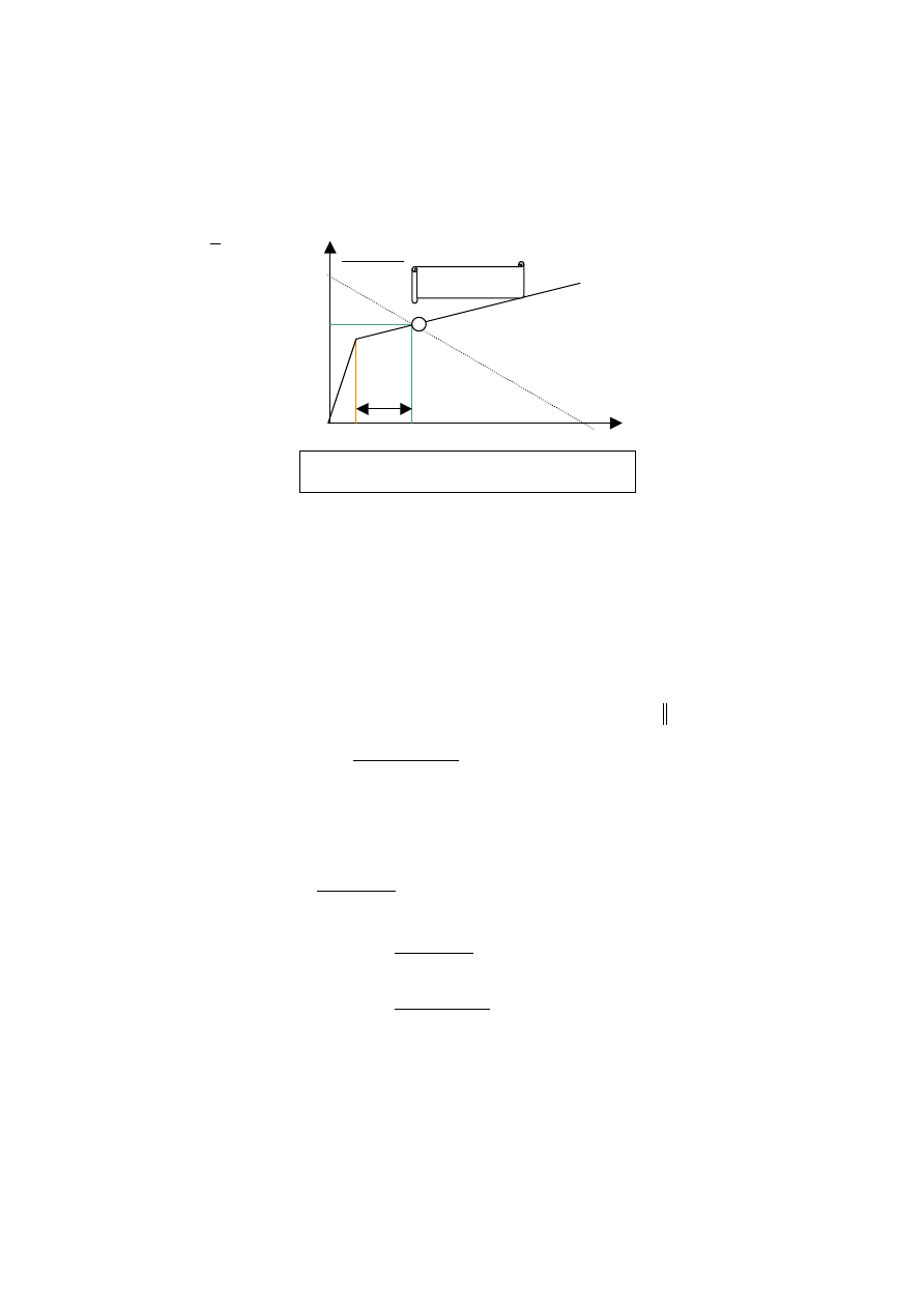
V
CE
I
C
V
CES
V
CEQ
I
CQ
V
outMax(-)
An npn transistor’s output characteristic.
V
CC
V
CC
R
C
+ R
E
Q-point
7/14
hand, the resistance
R
B
= R
1
R
2
should be greater than r
b’e
(hereinafter
computed) so that it’s shunting influence will not cause a significant
signal amplitude loss.
Let
I
R1
= 30I
B
and
I
B
+ I
R1
+ I
R 2
= 0
R
1
=
V
CC
V
B
30 I
BQ
,
R
2
=
V
B
31 I
BQ
The 2N3904 model‘s the ß
0
factor amounts to 178 at T=300
o
K, so:
I
BQ
=
I
CQ
0
=
2.7mA
178
= 0.015mA
,
so:
R
1
= 37.436k ,
R
2
= 11.084k
Now we might as well calculate the base resistance R
B
. We are going
to find it useful further on.
R
B
= R
1
R
2
=
R
1
R
2
R
1
+ R
2
,
R
B
= 8.552k
Having now calculated the resistor values of the BJT amplifier we are
going to compute it‘s variable constituents.
To find the capacities C
1
, C
C
and C
E
we have to calculate the
equivalent resistances seen from their ports.
The f
LC1
high-pass frequency
is related to the C
1
capacitance.
R
C1
= R
S
+
R
B
r
b' e
R
B
+ r
b' e
where:
r
b' e
=
0 T
I
CQ
,
T
=
kT
q
, k –
the Boltzmann constant, T –
temperature absolulte scale and q
– the charge of an electron.
So
T
= 0.026
and
r
b' e
= 1.714k
:
R
C1
= 23.428k
The f
LCC
high-pass frequency is related to the C
C
capacitance.
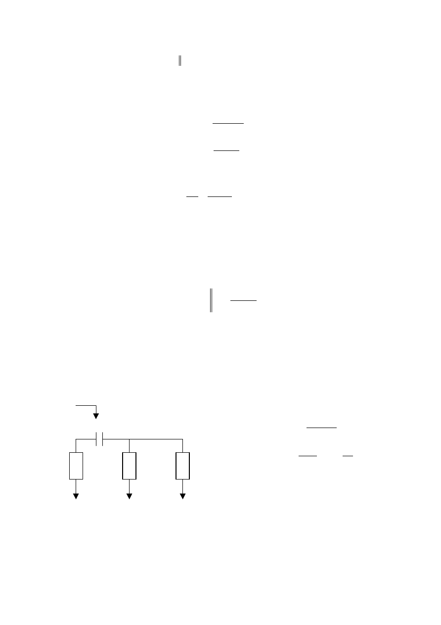
R
G
R
B
r
b‘e
C
1
R
C1
8/14
R
CC
= R
C
+ R
L
R
CC
= 34.931k
The f
LCE
high-pass
frequency is related to the C
E
capacitance.
R
CE
= R
E
||
r
b' e
+ R
S
|| R
B
0
+ 1
,
R
CE
= 0.043k
Since
f
L
=
f
LC1
2
+ f
LCC
2
+ f
LCE
2
=
1
2 C
1
R
C1
2
+
1
2 C
C
R
CC
2
+
1
2 C
E
R
CE
2
and R
CE
is the smallest of all the above calculated resistances let it be the
dominating pole of the lower cut-off frequency. I.e.:
C
E
=
1
2 R
CE
f
L
,
C
E
= 168
µ
F
Now let f
LC1
and f
LCC
be tolerable aberrations of f
L
and let them
amount to the value 1kHz. So:
C
1
=
1
2 R
C1
f
LC1
= 6.8
µ
F,
C
C
=
1
2 R
CC
f
LCC
= 4.5
µ
F
The input and output impedances:
R
IN
= R
B
|| r
b' e
= 1.427k
R
OUT
= R
C
|| h
22
= 2.931k
The voltage and current amplifications:
g
m
U
b‘e
R
C
C
C
R
L

9/14
k
v
=
V
OUT
V
IN
=
R
IN
g
m
R
L
R
IN
+ R
S
= 202.717
k
i
= k
v
R
S
R
L
= 139.368
The high frequency cut-off:
f
H
=
1
2 (R
IN
|| R
S
)(C
je
+ C
jc
+ C
jc
g
m
R
L
)
,
where the C
jc
and C
je
can be found in the zad1.out bias point
calculations, their values for junction temperature 27
o
C 1.96pF and
65.8pF respectively.
f
H
= 193.1kHz
Obviously this value is way beyond the desired high cut-off
frequency. Because the calculated f
H
is disproportionately higher than the
specified one we have to solve the matter somehow.
Adding a capacitor C
L
parallelly to the R
L
resistor is one option,
because the additional capacity will serve us as a low-pass filter thus
limiting the high cut-off frequency.
The resistance as seen from the ports of C
L
:
R
CL
= R
C
|| R
L
= 2.685k
So:
C
L
=
1
2 R
CL
f
H
= 1.411nF
Summary:
Obtained values:
V
CEQ
8.25V
I
CQ
2.7mA
V
outMax
7.25V
R
C
2.931kΩ
R
E
2.162kΩ
R
1
37.436kΩ
R
2
11.084kΩ
I
BQ
0.015mA
R
B
8.552kΩ
C
1
6.8uF
C
C
4.5uF
C
E
168uF
r
b’e
1.714kΩ

10/14
R
IN
1.427kΩ
R
OUT
2.931kΩ
k
v
202.717
k
i
139.368
11/14
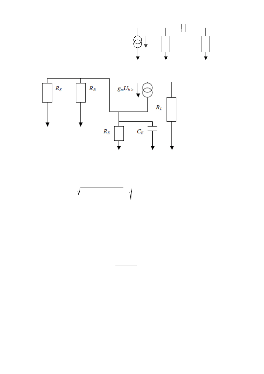
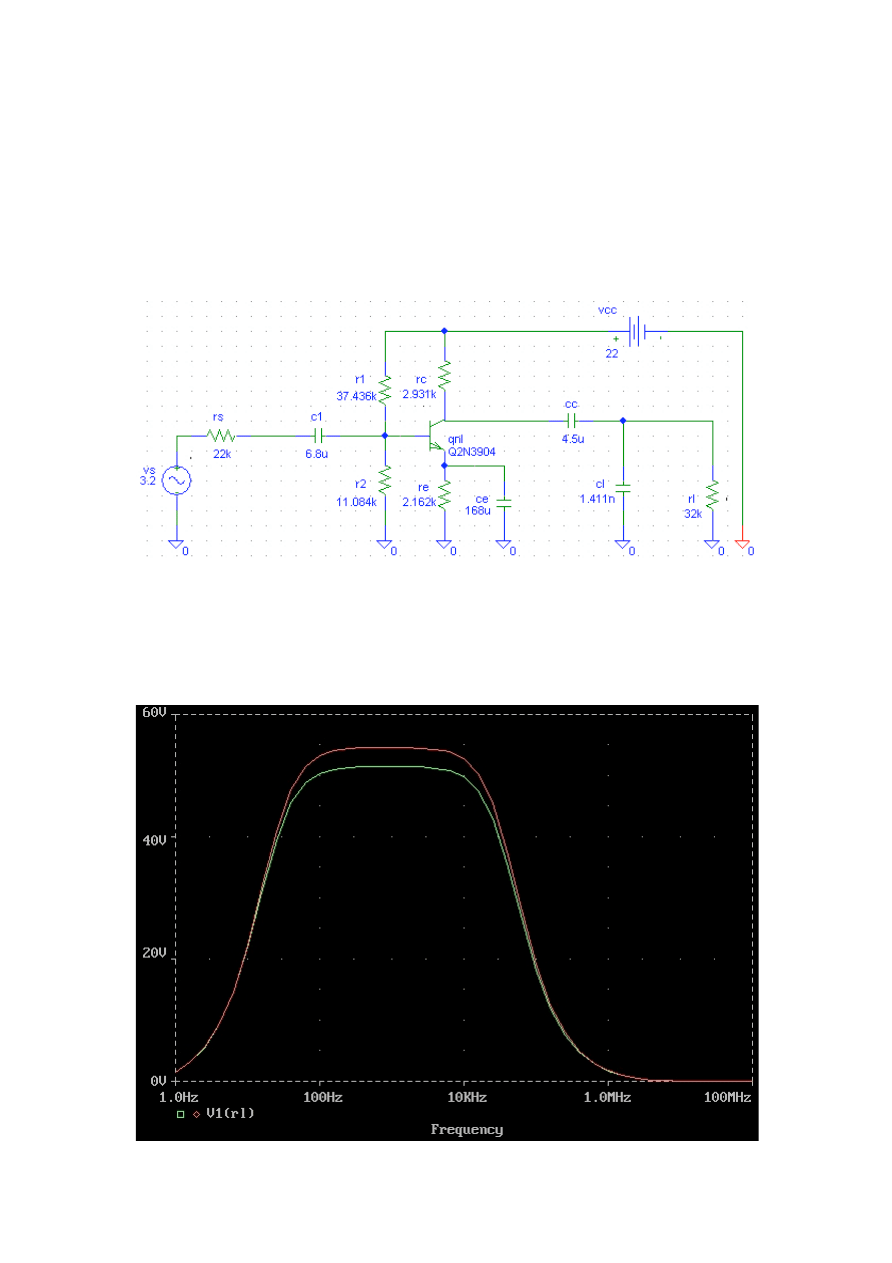
Task 3. Amplifier Investigation - part 2
Design the amplifier from the second task using the Pspice
simulator. Compare the hand calculations results with the Pspice
results using the DC, AC and Transient analyses. Analyse the
maximum output amplitude and THD for the output signal.
The amplifier schematic:
This image was made only as a reference. The analysis was
performed in text mode. The zad3.out print is enclosed with the project
documentation.
Below is the output voltage characteristic:
12/14
The lower and upper cut-off frequency slightly differs from the
expected one due to the capacitor C
L
added for better control of the
bandwidth.
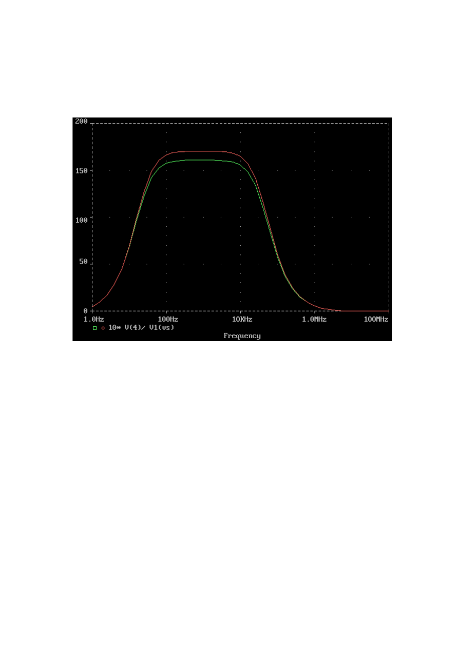
The voltage amplification characteristic:
The efficient voltage amplification factor for T=27
o
C is slightly lower
than that which was calculated. This is a fault of precision. As was
anticipated, along with the temperature growth the amplifier’s parameters
have worsened. The effective amplification factor is lower.
13/14
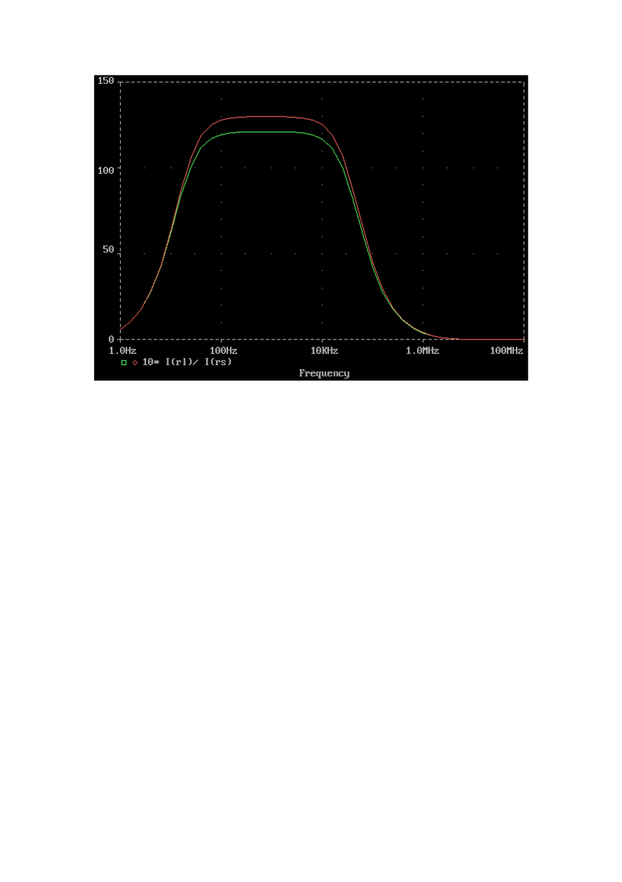
The value of the efficient current amplification are satisfyingly
similar to those calculated in task 2. As seen in the graph above the
currrent amplification factor grows with the temperature.
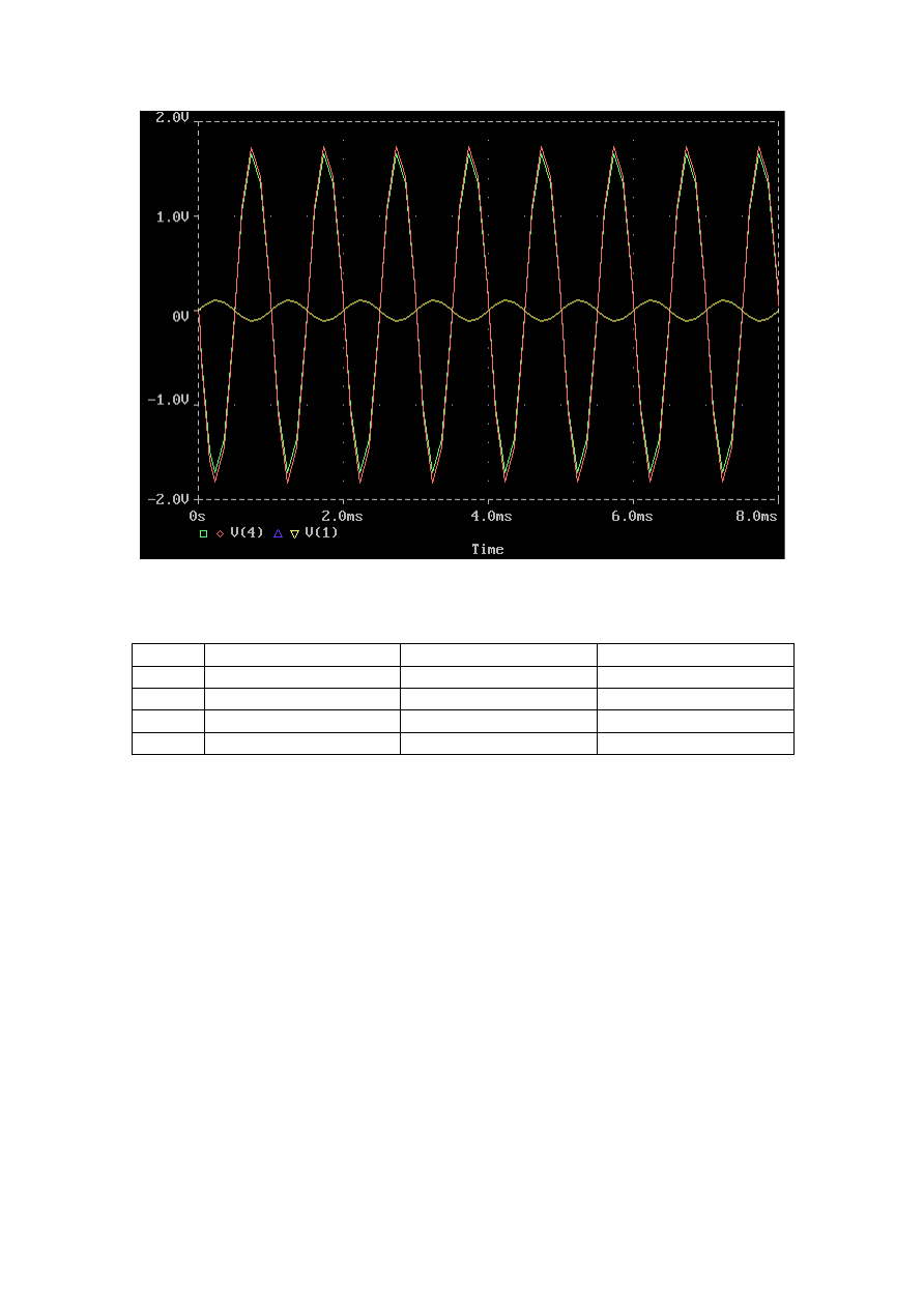
Below is the simulation of the input and output signals:
14/14
This illustrates the dependency of the input and output signals. The
output signal has a reverse phase to the input signal. The efficient voltage
amplification grows with the temperature.
Hand calculations
T=27
o
C
T=52
o
C
k
v
202.717
188.292
176.103
k
i
139.368
120.93
129.83
f
L
22Hz
21.343Hz
22.414Hz
f
H
42kHz
39.708kHz
39.483kHz
The results from the simulation differ from the ones that were
calculated by hand, though the differences are not of a significant rank
and are due to the lack of precision of all hand calculations in general.
Temperature aberrations have an unfavorable influence on the
properties of BJT amplifiers. This is why designing a circuit the designer
should also estimate it’s behaviour in various ambient conditions. The
negative feedback introduced by R
E
stabilizes the Q-point of the
amplifier. It reduces the influence of temperature to the circuit‘s
properties.
Wyszukiwarka
Podobne podstrony:
PN EN 1991 1 2 2006 Ap1 2010
PN EN 12697 7 2006 06 30
PN EN 1993 1 1 2006
PN EN 1993 1 8 2006 AP2 2011
PN EN 1991 1 2 2006
Hydronic 5SC 12Volt TD 07 2006 EN JE
pn en iso 14688 2 2006 www przeklej pl
PN EN 1993 1 1 2006 AC 2009
PN EN 1993 1 8 2006
2006 04 27 study oil prices transport en
PN EN 1991 1 2 2006 AC 2009
PN EN 1993 1 1 2006 Projekt konstr stalowych
Bud Kufo 2006 en
PN EN 1991 1 2 2006 Ap1 2010
En Passant Chess Magazine No 105, 2006 11 (Italian)
PN EN 1993 1 1 2006 Projekt konstr stalowych
więcej podobnych podstron