HCC4029B
HCF4029B
September 1988
BINARY OR BCD DECADE
PRESETTABLE UP/DOWN COUNTER
EY
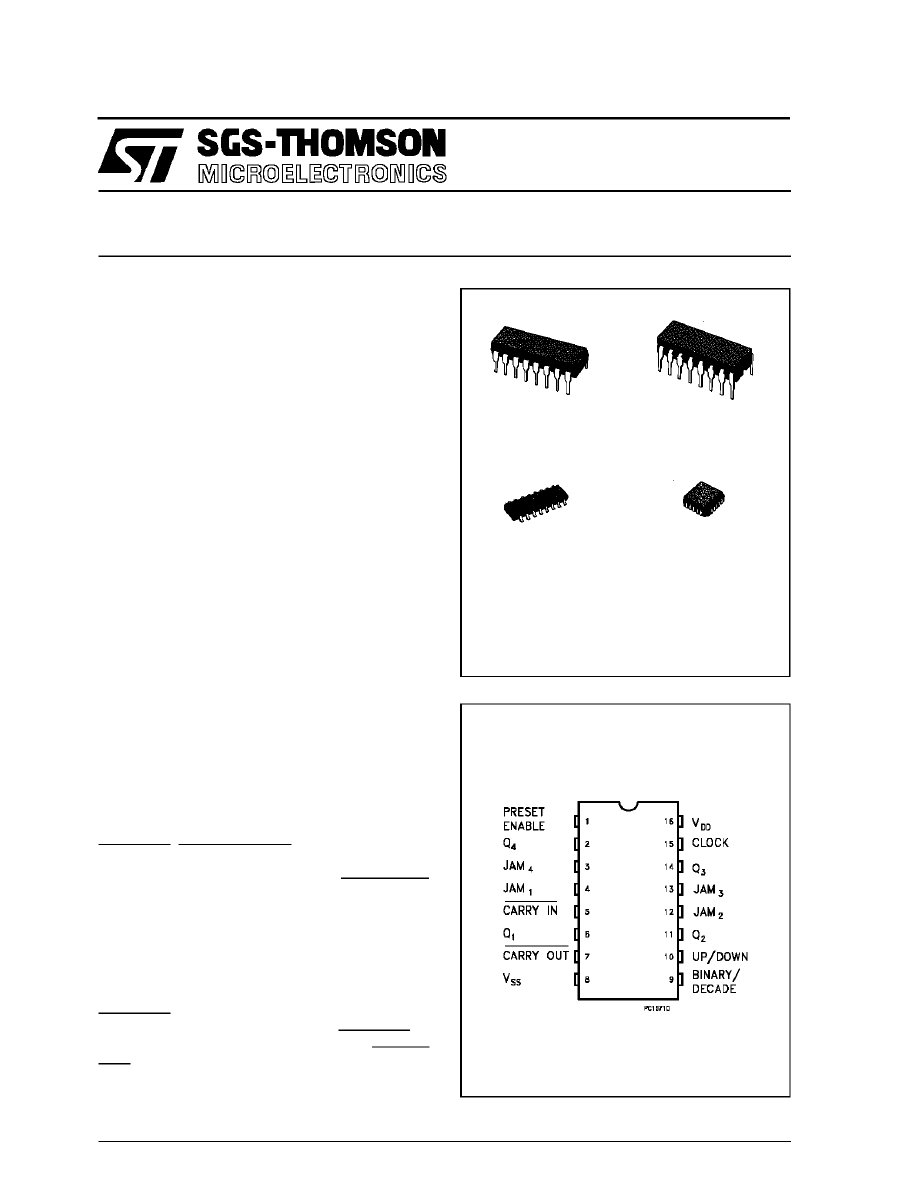
(Plastic Package)
DESCRIPTION
ORDER CODES :
HCC4029BF
HCF4029BM1
HCF4029BEY
HCF4029BC1
F
(Ceramic Package)
M1
(Micro Package)
C1
(Chip Carrier)
PIN CONNECTIONS
NC = No Internal Connection
The HCC4029B (extended temperature range) and
HCF4029B (intermediate temperature range) are
monolithic integrated circuit, available in 16-lead
dual in-line plastic or ceramic package and plastic
micro package. The HCC/HCF4029B consists of a
four-stage binary or BCD-decade up/down counter
with provisions for look-ahead carry in both counting
modes. The inputs consist of a single CLOCK,
CARRY-IN (CLOCK ENABLE), BINARY/DECADE,
UP/DOWN, PRESET ENABLE, and four individual
JAM signals. Q1, Q2, Q3, Q4 and a CARRY OUT
signal are provided as outputs. A high PRESET EN-
ABLE signal allows information on the JAM INPUTS
to preset the counter to any state asynchronously
with the clock. A low on each JAM line, when the
PRESET-ENABLE signal is high, resets the counter
to its zero count. The counter is advanced one count
at the positive transition of the clock when the
CARRY-IN and PRESET ENABLE signals, are low.
Advancement is inhibited when the CARRY-IN or
PRESET ENABLE signals are high. The CARRY-
OUT signal is normally high and goes low when the
.
MEDIUM SPEED OPERATION - 8MHz (typ.) @
C
L
= 50pF AND V
DD
-V
SS
= 10V
.
MULTI-PACKAGE PARALLEL CLOCKING FOR
SYNCHRONOUS HIGH SPEED OUTPUT RES-
PONSE OR RIPPLE CLOCKING FOR SLOW
CLOCK INPUT RISE AND FALL TIMES
.
”PRESET ENABLE” AND INDIVIDUAL ”JAM”
INPUTS PROVIDED
.
BINARY OR DECADE UP/DOWN COUNTING
.
BCD OUTPUTS IN DECADE MODE
.
STANDARDIZED
SYMMETRICAL
OUTPUT
CHARACTERISTICS
.
5V, 10V, AND 15V PARAMETRIC RATINGS
.
INPUT CURRENT OF 100nA AT 18V AND 25
°
C
FOR HCC DEVICE
.
QUIESCENT CURRENT SPECIFIED TO 20V
FOR HCC DEVICE
.
100% TESTED FOR QUIESCENT CURRENT
.
MEETS ALL REQUIREMENTS OF JEDEC TEN-
TATIVE STANDARD N
o
. 13A, ”STANDARD
SPECIFICATIONS FOR DESCRIPTION OF ”B”
SERIES CMOS DEVICES”
1/13
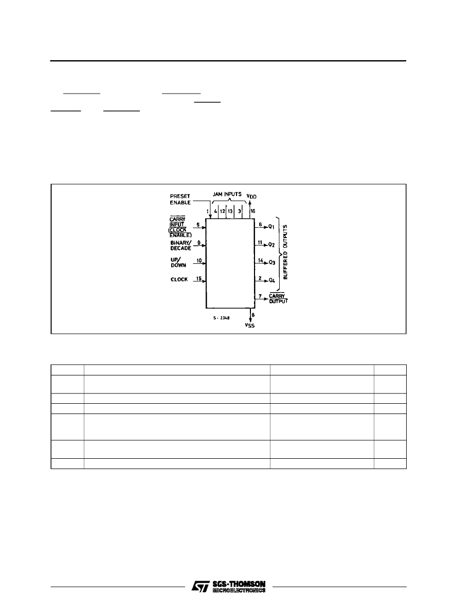
counter reaches its maximum count in the UP mode
or the minimum count in the DOWN mode provided
the CARRY-IN signal is low. The CARRY-IN signal
in the low state can thus be considered a CLOCK
ENABLE. The CARRY-IN terminal must be con-
nected to V
SS
when not in use. Binary counting is ac-
complished when the BINARY/DECADE input is
high ; the counter counts in the decade mode when
the BINARY/DECADE input is low. The counter
counts Up when to UP/DOWN INPUT is high, and
Down when the UP/DOWN INPUT is low. Multiple
packages can be connected in either a parallel-
clocking or a ripple-clocking arrangement as shown
in cascading counter packages. Parallel clocking
provides synchronous control and hence faster re-
sponse from all counting outputs. Ripple-clocking
allows for longer clock input rise and fall times.
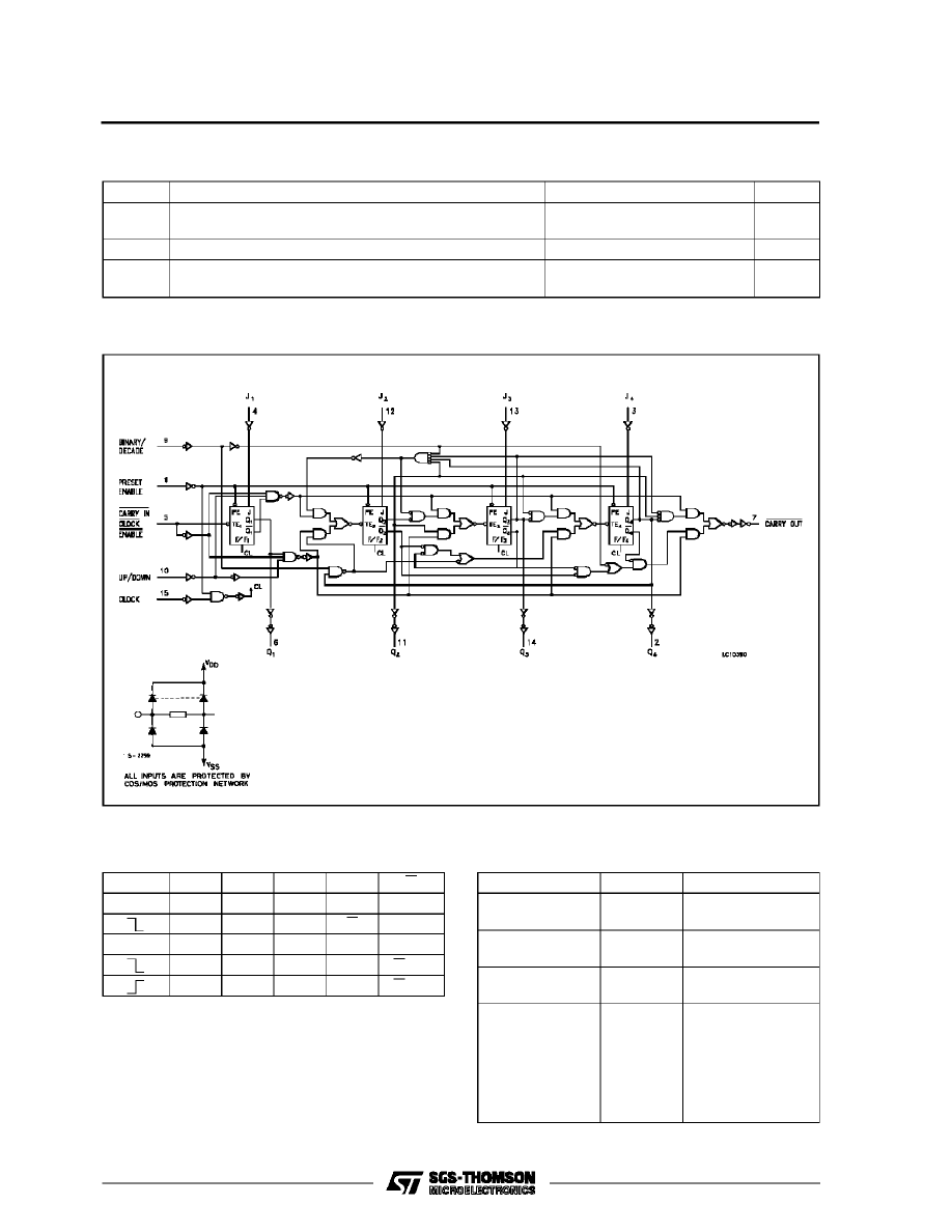
FUNCTIONAL DIAGRAM
ABSOLUTE MAXIMUM RATING
Symbol
Parameter
Value
Unit
V
DD
*
Supply Voltage: HCC Types
HCF Types
-0.5 to +20
-0.5 to +18
V
V
V
i
Input Voltage
-0.5 to V
DD
+ 0.5
V
I
I
DC Input Current (any one input)
±
10
mA
P
tot
Total Power Dissipation (per package)
Dissipation per Output Transistor
for Top = Full Package Temperature Range
200
100
mW
mW
T
op
Operating Temperature: HCC Types
HCF Types
-55 to +125
-40 to +85
o
C
o
C
T
stg
Storage Temperature
-65 to +150
o
C
Stresses above those listed under ”Absolute Maximum Ratings” may cause permanent damage to the device. This is a stress ratingonly and functional
operation of the device at these or any other conditions above those indicated in the operational sections of this specification is not implied. Exposure
to absolute maximum rating conditions for external periods may affect device reliability.
All voltage values are referred to V
SS
pin voltage.
HCC/HCF4029B
2/13
RECOMMENDED OPERATING CONDITIONS
Symbol
Parameter
Value
Unit
V
DD
Supply Voltage: HCC Types
HCF Types
3 to 18
3 to 15
V
V
V
I
Input Voltage
0 to V
DD
V
T
op
Operating Temperature: HCC Types
HCF Types
-55 to +125
-40 to +85
o
C
o
C
LOGIC DIAGRAMS
TRUTH TABLES
CLOCK
TE
PE
J
Q
Q
X
X
O
O
O
I
O
I
X
Q
Q
X
X
O
I
I
O
I
I
X
Q
Q NC
X
I
X
Q
Q NC
X DON’T CARE
Control Input
Logic Level
Action
BIN/DEC
(B/D)
I
O
Binary Count
Decade Count
UP/DOWN
(U/D)
I
O
Up Count
Down Count
Preset Enable
(PE)
I
O
Jam In
No Jam
Carry In (Cl)
(Clock Enable)
I
O
No Counter
Advance at Pos.
Clock Transition
Advance Counter
at Pos. Clock
Transition
HCC/HCF4029B
3/13
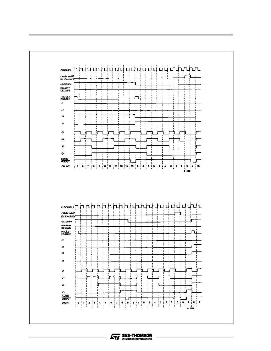
TIMING DIAGRAMS
Binary Mode
Decade Mode
HCC/HCF4029B
4/13
STATIC ELECTRICAL CHARACTERISTICS (over recommended operating conditions)
Symbol
Parameter
Test Conditios
Value
Unit
V
I
(V)
V
O
(V)
|I
O
|
(
µ
A)
V
DD
(V)
T
LOW
*
25
o
C
T
HIGH
*
Min.
Max.
Min.
Typ.
Max.
Min.
Max.
I
L
Quiescent
Current
HCC
Types
0/5
5
5
0.04
5
150
µ
A
0/10
10
10
0.04
10
300
0/15
15
20
0.04
20
600
0/20
20
100
0.08
100
3000
HCF
Types
0/5
5
20
0.04
20
150
0/10
10
40
0.04
40
300
0/15
15
80
0.04
80
600
V
OH
Output High
Voltage
0/5
< 1
5
4.95
4.95
4.95
V
0/10
< 1
10
9.95
9.95
9.95
0/15
< 1
15
14.95
14.95
14.95
V
OL
Output Low
Voltage
5/0
< 1
5
0.05
0.05
0.05
V
10/0
< 1
10
0.05
0.05
0.05
15/0
< 1
15
0.05
0.05
0.05
V
IH
Input High
Voltage
0.5/4.5
< 1
5
3.5
3.5
3.5
V
1/9
< 1
10
7
7
7
1.5/13.5
< 1
15
11
11
11
V
IL
Input Low
Voltage
4.5/0.5
< 1
5
1.5
1.5
1.5
V
9/1
< 1
10
3
3
3
13.5/1.5
< 1
15
4
4
4
I
OH
Output
Drive
Current
HCC
Types
0/5
2.5
5
-2
-1.6
-3.2
-1.15
mA
0/5
4.6
5
-0.64
-0.51
-1
-0.36
0/10
9.5
10
-1.6
-1.3
-2.6
-0.9
0/15
13.5
15
-4.2
-3.4
-6.8
-2.4
HCF
Types
0/5
2.5
5
-1.53
-1.36
-3.2
-1.1
0/5
4.6
5
-0.52
-0.44
-1
-0.36
0/10
9.5
10
-1.3
-1.1
-2.6
-0.9
0/15
13.5
15
-3.6
-3.0
-6.8
-2.4
I
OL
Output
Sink
Current
HCC
Types
0/5
0.4
5
0.64
0.51
1
0.36
mA
0/10
0.5
10
1.6
1.3
2.6
0.9
0/15
1.5
15
4.2
3.4
6.8
2.4
HCF
Types
0/5
0.4
5
0.52
0.44
1
0.36
0/10
0.5
10
1.3
1.1
2.6
0.9
0/15
1.5
15
3.6
3.0
6.8
2.4
I
IH
, I
IL
Input
Leakage
Current
HCC
Types
0/18
Any Input
18
±
0.1
±
10
-5
±
0.1
±
1
µ
A
HCF
Types
0/15
15
±
0.3
±
10
-5
±
0.3
±
1
C
I
Input Capacitance
Any Input
5
7.5
pF
* T
LOW
= -55
o
C for HCC device: -40
o
C for HCF device.
* T
HIGH
= +125
o
C for HCC device: +85
o
C for HCF device.
The Noise Margin for both ”1” and ”0” level is: 1V min. with V
DD
= 5 V, 2 V min. with V
DD
= 10 V, 2.5 V min. with V
DD
= 15 V
HCC/HCF4029B
5/13
DYNAMIC ELECTRICAL CHARACTERISTICS (T
amb
= 25
o
C, C
L
= 50 pF, R
L
= 200 K
Ω
,
typical temperature coefficent for all V
DD
values is 03 %/
o
C, all input rise and fall times= 20 ns)
Symbol
Parameter
Test Conditions
Value
Unit
V
DD
(V)
Min.
Typ.
Max.
t
PLH
t
PHL
Propagation Delay Time (Q Outputs)
5
250
500
ns
10
120
240
15
90
180
t
PLH
t
PHL
Propagation Delay Time (Carry Output)
5
280
560
ns
10
130
260
15
95
190
t
TLH
t
THL
Transition Time (Q Outputs, Carry Output)
5
100
200
ns
10
50
100
15
40
80
t
W
Minimum Clock Pulse Width
5
90
180
ns
10
45
90
15
30
60
t
r
, t
f
**
Clock Rise and Fall Time
5
15
µ
s
10
15
15
15
t
setup
*
Minimum Setup Time (Carry Input)
5
30
60
ns
10
10
20
15
6
12
t
setup
Minimum Setup Time (B/D or UD)
5
170
340
10
70
140
15
50
100
f
max
Maximum Clock Input Frequency
5
2
4
MHz
10
4
8
15
5.5
11
PRESET ENABLE
t
PLH
t
PHL
Propagation Delay Time (Q Outputs)
5
235
470
ns
10
100
200
15
80
160
t
PLH
t
PHL
Propagation Delay Time (Carry Output)
5
320
640
10
145
290
15
105
210
t
W
Minimum Preset Enable (Pulse Width)
5
65
130
ns
10
35
70
15
25
50
t
rem
*
Minimum Preset Enable (Removal Time)
5
100
200
ns
10
55
110
15
40
80
CARRY INPUT
t
PHL
t
PLH
Propagation Delay Time (Carry Output)
5
170
340
ns
10
70
140
15
50
100
t
setup
***
Minimum Setup Time (Carry In)
5
25
50
ns
10
15
30
15
12
25
t
hold
Minimum Hold Time (Carry In)
5
100
200
10
35
70
15
30
60
*
From Up/Down, Binary/Decade, Carry In or Preset Enable Control Inputs to Clock Edge
** If more than one unit is cascated in the parallel clocked application tr should be made less than or equal to the sum of the fixed propagation
delay at 15 pF and the transition time of the carry output driving stage for the estimated capacitance load.
*** From Carry in to Clock Edge.
HCC/HCF4029B
6/13

Typical Output Low (sink) Current Characteristics.
Minimum Output Low (sink) Current Charac-
Typical Output High (source) Current Charac-
teristics.
Minimum Output High (source) Current Charac-
teristics.
HCC/HCF4029B
7/13
APPLICATIONS
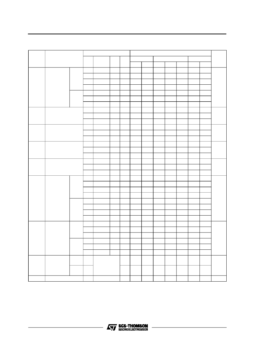
Conversion of Clock up, Clock Down Input Sig-
nals to Clock and Up/Down Inputs Signals.
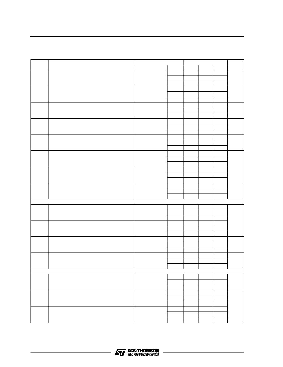
Cascading Counter Packages.
The HCC/HCF4029B CLOCK and UP/DOWN in-
puts are used directly in most applications. In appli-
cations where CLOCK UP and CLOCK DOWN
inputs
are
provided,
conversion
to
the
HCC/HCF4029B CLOCK and UP/DOWN inputs
can easily be realized by use of the circuit.
HCC/HCF4029B changes count on positive transi-
tions of CLOCK UP or CLOCK DOWN inputs. For
the gate configuration shown below, when counting
up the CLOCK DOWN input must be maintained
high and conversely when counting down the
CLOCK UP input must be maintained high.
*
CARRY-OUT lines at the 2nd, 3rd, et., stages may have a negative-going glitch pulse resulting from differential delays of different
HCC/HCF4029B IC’s. These negative-going glitches do not affect proper HCC/HCF4029B operation. However, if the CARRY-OUT signals
are used to trigger other edge-sensitive logic devices, such as FF’s or counters, the CARRY-OUT signals should be gated with the clock signal
using a 2-input NOR gate such as HCC/HCF4001B.
Ripple Clocking Mode : The Up/Down control can be changed at any count. The only restriction on changing the Up/Down control is that the
clock input to the first counting stage must be high.
HCC/HCF4029B
8/13
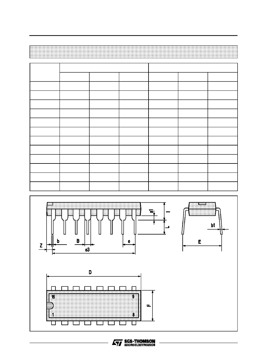
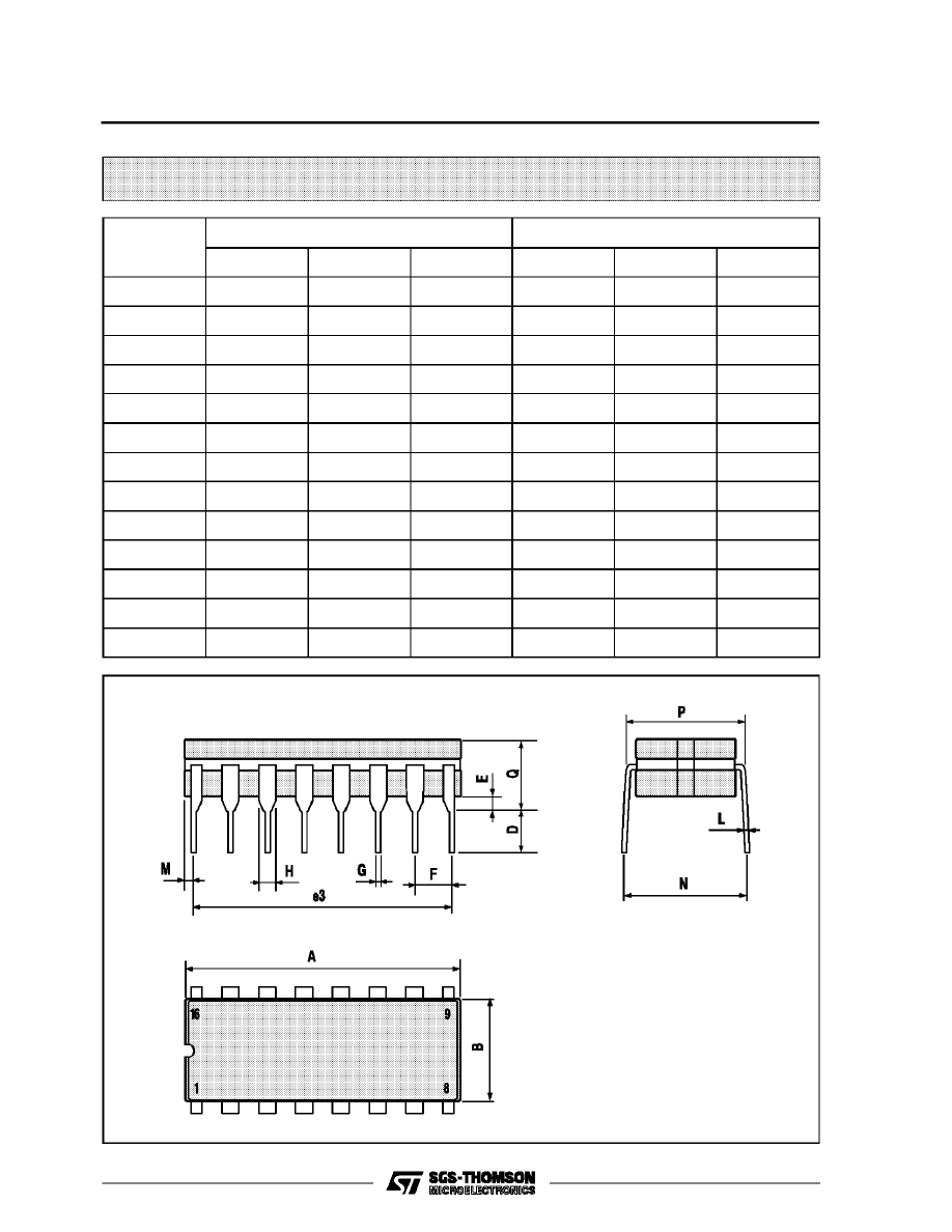
Plastic DIP16 (0.25) MECHANICAL DATA
DIM.
mm
inch
MIN.
TYP.
MAX.
MIN.
TYP.
MAX.
a1
0.51
0.020
B
0.77
1.65
0.030
0.065
b
0.5
0.020
b1
0.25
0.010
D
20
0.787
E
8.5
0.335
e
2.54
0.100
e3
17.78
0.700
F
7.1
0.280
I
5.1
0.201
L
3.3
0.130
Z
1.27
0.050
P001C
HCC/HCF4029B
9/13
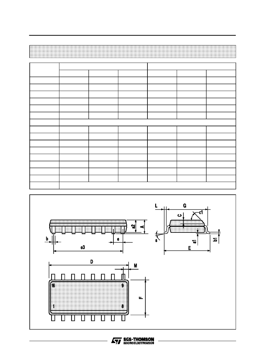
Ceramic DIP16/1 MECHANICAL DATA
DIM.
mm
inch
MIN.
TYP.
MAX.
MIN.
TYP.
MAX.
A
20
0.787
B
7
0.276
D
3.3
0.130
E
0.38
0.015
e3
17.78
0.700
F
2.29
2.79
0.090
0.110
G
0.4
0.55
0.016
0.022
H
1.17
1.52
0.046
0.060
L
0.22
0.31
0.009
0.012
M
0.51
1.27
0.020
0.050
N
10.3
0.406
P
7.8
8.05
0.307
0.317
Q
5.08
0.200
P053D
HCC/HCF4029B
10/13
SO16 (Narrow) MECHANICAL DATA
DIM.
mm
inch
MIN.
TYP.
MAX.
MIN.
TYP.
MAX.
A
1.75
0.068
a1
0.1
0.2
0.004
0.007
a2
1.65
0.064
b
0.35
0.46
0.013
0.018
b1
0.19
0.25
0.007
0.010
C
0.5
0.019
c1
45
°
(typ.)
D
9.8
10
0.385
0.393
E
5.8
6.2
0.228
0.244
e
1.27
0.050
e3
8.89
0.350
F
3.8
4.0
0.149
0.157
G
4.6
5.3
0.181
0.208
L
0.5
1.27
0.019
0.050
M
0.62
0.024
S
8
°
(max.)
P013H
HCC/HCF4029B
11/13
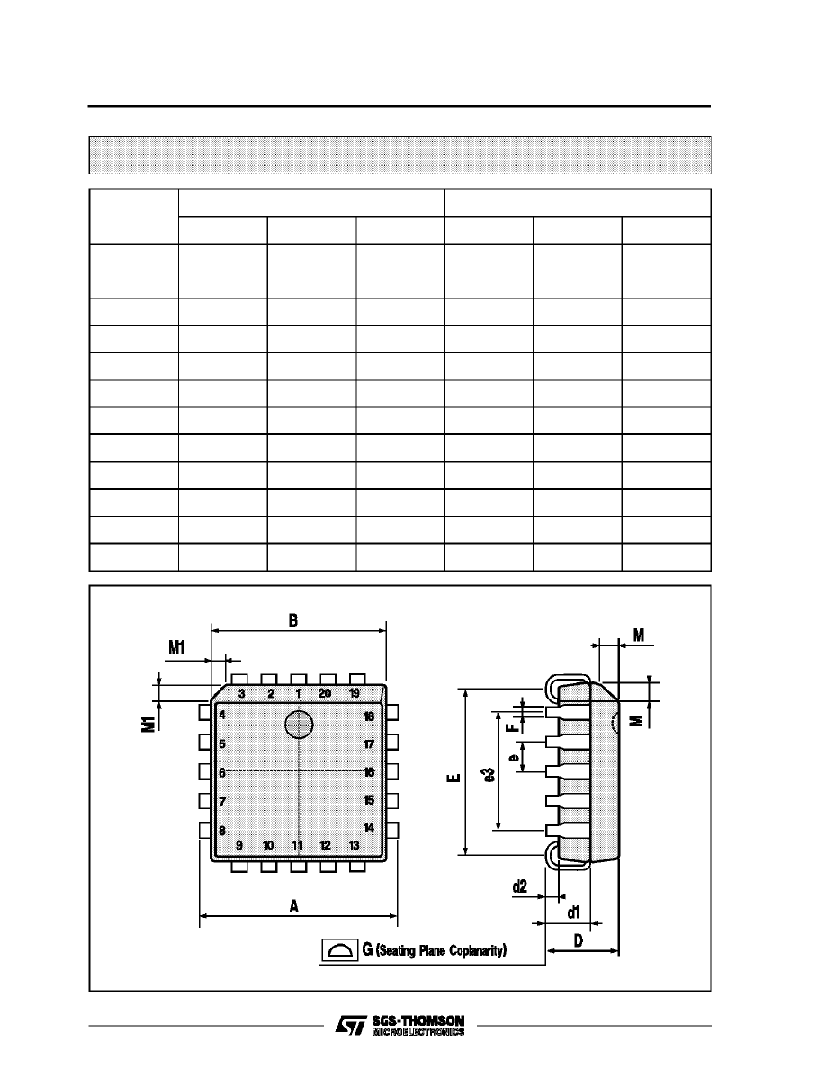
PLCC20 MECHANICAL DATA
DIM.
mm
inch
MIN.
TYP.
MAX.
MIN.
TYP.
MAX.
A
9.78
10.03
0.385
0.395
B
8.89
9.04
0.350
0.356
D
4.2
4.57
0.165
0.180
d1
2.54
0.100
d2
0.56
0.022
E
7.37
8.38
0.290
0.330
e
1.27
0.050
e3
5.08
0.200
F
0.38
0.015
G
Wyszukiwarka
Podobne podstrony:
4029
4029 ac
4029 (Philips) id 38390 Nieznany (2)
4029
4029
4029
4029
4029
4029
więcej podobnych podstron