L9308
October 1990
DUAL LOW SIDE DRIVER
.
DARLINGTON OUTPUT STAGE
.
INPUT COMPARATOR WITH WIDE RANGE
COMMON MODE OPERATION AND GROUND
COMPATIBLE INPUTS
.
INPUT COMPARATOR HYSTERESIS
.
SHORT CIRCUIT PROTECTION OF OUTPUT
WITH SOA PROTECTION
.
INTERNAL THERMAL PROTECTION WITH
HYSTERESIS
.
SINGLESUPPLY VOLTAGEFROM 3.5VUP TO
28V
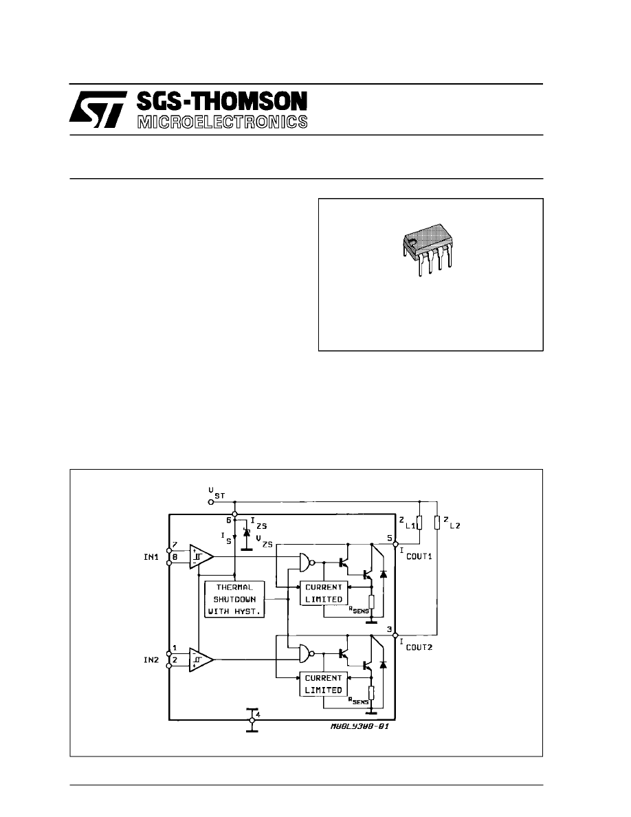
DESCRIPTION
The L9308 is a monolithic interface circuit with dif-
ferentialinput comparator and open collector output
able to sink current specifically to drive lamps, re-
lays, d.c. motors, electro valves etc.
Particular care has been taken to protect the device
against destructive failures - short circuit of outputs
to V
S
, SOA protection, supply overvoltage.
BLOCK DIAGRAM
ORDERING NUMBER : L9308
MINIDIP
A built in thermal shut-down switches off the device
when the IC’s internal dissipation becomes too high
and the chip temperature exceeds the security
threshold.
The input comparatorhysteresis increases the inter-
face’s noise immunity allowing the correct use in
critical environments as automotive applications.
1/7
This is advanced information on a new product now in development or undergoing evaluation. Details are subject to change without notice.
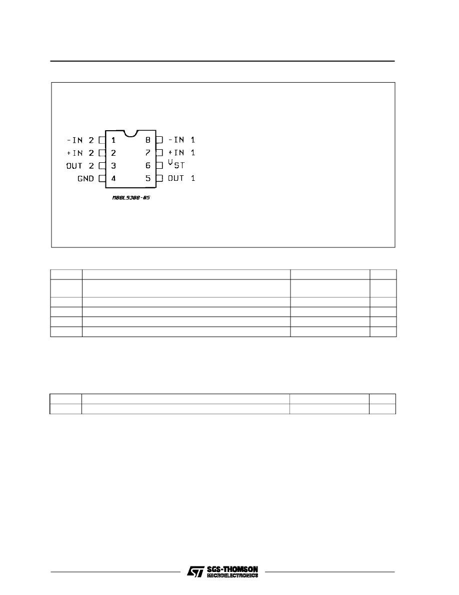
PIN CONNECTION (Top view)
ABSOLUTE MAXIMUM RATINGS
Symbol
Parameter
Value
Unit
I
ZS
Current Into Supply
Tamb = 25
°
C, DC
Clamp Zener Diode
Pulsed (*)
30
80
mA
mA
V
S
Supply Voltage
28
V(**)
I
O
Output Current
Internally Limited
T
j
, T
stg
Junction and Storage Temperature
– 55 to +150
°
C
P
tot
Power Dissipation at T
amb
= 85
°
C
650
mW
(*) TON
≤
2.5ms ; repetition time > 30ms.
(**) The maximum allowed supply voltage without limiting resistor is limited by the built-in protection zener diode : see V
ZS
spec.
values. If V
S
is higher than V
ZS
a resistor R
S
is necessary to limit the zener current I
ZS
.
THERMAL DATA
Symbol
Parameter
Value
Unit
R
th j-amb
Thermal Resistance Junction-ambient
Max
100
°
C/W
1) -IN2
Inverting input2
2) +IN2
Non-inverting input2
3) OUT2 Output2
4) GND Ground
5) OUT1 Output1
6) V
ST
Supply
7) +IN1
Non-inverting input1
8) -IN1
Inverting input1
L9308
2/7
ELECTRICAL CHARACTERISTICS (V
s
= 14.4V ; – 40
°
C
≤
T
amb
,
≤
85
°
C; R
S
= 100
Ω
unless otherwise noted)
Symbol
Parameter
Test Conditions
Min.
Typ.
Max.
Unit
V
IH
Hysteresis of the Input
Comparater
V
IN
= 200mVpp ;
f = 1kHz
20
80
mV
I
B
Input Bias Current
V
I
+
= V
I
–
= 0
0.2
1.0
µ
A
I
OS
Input Offset Current
V
I
+
= V
I
–
= 0
±
50
±
400
nA
CMR
Input Common Mode Range
V
s
= 6 – 18V
T
amb
= 25
°
C
0
V
ST
–1.6
V
I
SC
Output Short Circuit Current for
Each Channel
(see fig. 4)
V
IN
– V
IN
> 70mV
V
S
= 16V
T
amb
= 25
°
C to 85
°
C
T
amb
= – 40
°
C to 25
°
C
V
OUT 1, 2
= 6V
0.6
0.7
1.2
A
A
A
V
CSAT
On Status Saturation Voltage
T
amb
= – 40
°
C to 25
°
C
V
I
–
– V
I
+
> 70mV
I
OUT 1, 2
= 300mA
T
amb
= 25
°
C to 85
°
C
1.0
1.5
1.4
V
V
I
OL
Output Leakage Current
V
I
–
– V
I
–
> 70mV
V
S
= 18V
V
S
= 5V
10
300
20
µ
A
µ
A
V
ST
Supply voltage (pin 6)
3.5
18
V
I
”st.by”
Supply Current
V
I
+
V
I
–
> 70mV
5
8
mA
I
”ON”
Supply Current
V
I
–
V
I
+
> 70mV
18
mA
V
ZS
Voltage Clamp Supply Protection
I
ZS
= 10mA
20
27
V
I
Omin
Minimum Output Current wiyth
the Outputs connected Together
V
CSAT
= 1.5V
400
mA
t
r
t
f
Rise Time (see fig. 2)
Fall Time
I
OUT
= 50mA
T
amb
= 25
°
C
2
2
µ
s
t
don
t
doff
Delay Time on
Delay Time off
I
OUT
= 50mA
T
amb
= 25
°
C
10
10
µ
s
L9308
3/7
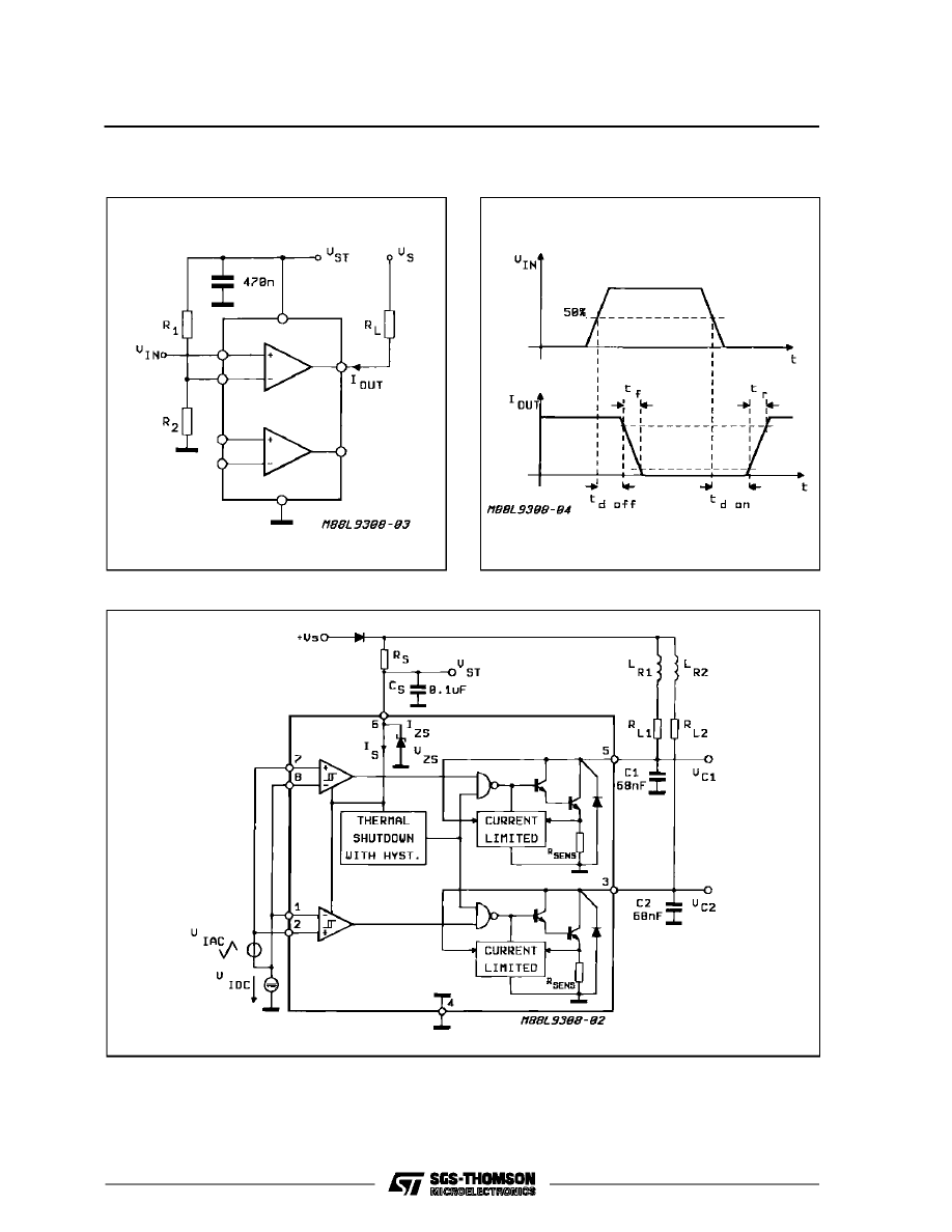
Figure 1 : Switching Time Test Circuit.
Figure 2 : Switching Time Waveforms for Resis-
tive Loads.
Figure 3 : Typical Application and Test Circuit.
Notes :
a) R
S requiredonly to limit
Ι
ZS
whenever V
S
exceeds V
ZS
voltage value.
b) C
1
, C
2
cut high frequency gain during current limiting.
L9308
4/7
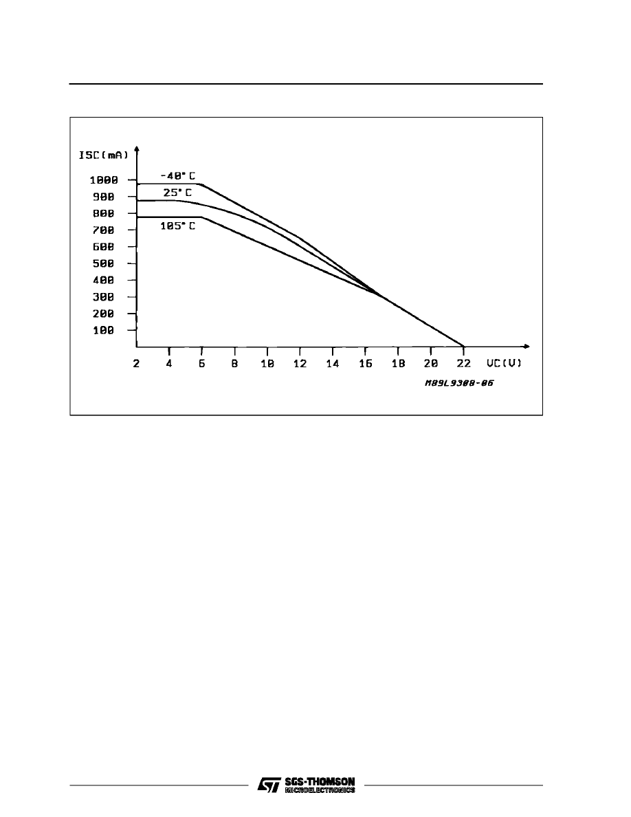
Figure 4 : Typical SOA Characteristic.
L9308
5/7
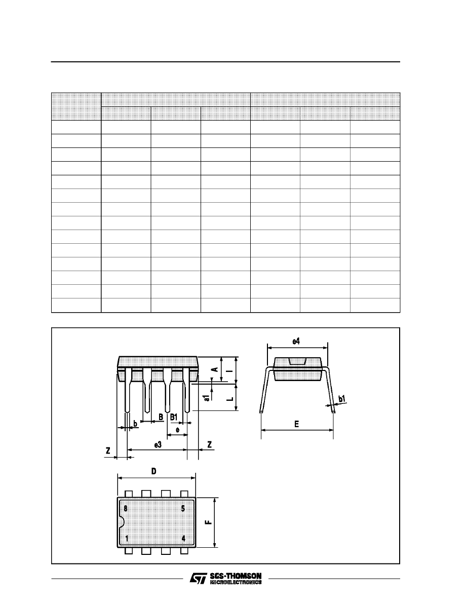
MINIDIP PACKAGE MECHANICAL DATA
DIM.
mm
inch
MIN.
TYP.
MAX.
MIN.
TYP.
MAX.
A
3.32
0.131
a1
0.51
0.020
B
1.15
1.65
0.045
0.065
b
0.356
0.55
0.014
0.022
b1
0.204
0.304
0.008
0.012
D
10.92
0.430
E
7.95
9.75
0.313
0.384
e
2.54
0.100
e3
7.62
0.300
e4
7.62
0.300
F
6.6
0.260
I
5.08
0.200
L
3.18
3.81
0.125
0.150
Z
1.52
0.060
L9308
6/7

Information furnished is believed to be accurate and reliable. However, SGS-THOMSON Microelectronics assumes no responsibility for
the consequences of use of such information nor for any infringement of patents or other rights of third parties which may result from its
use. No license is granted by implication or otherwise under any patent or patent rights of SGS-THOMSON Microelectronics. Specifica-
tions mentioned in this publication are subject to change without notice. This publication supersedes and replaces all information pre-
viously supplied. SGS-THOMSON Microelectronics products are not authorized for use as critical components in life support devices or
systems without express written approval of SGS-THOMSON Microelectronics.
1994 SGS-THOMSON Microelectronics - All Rights Reserved
SGS-THOMSON Microelectronics GROUP OF COMPANIES
Australia - Brazil - France - Germany - Hong Kong - Italy - Japan - Korea - Malaysia - Malta - Morocco - The Netherlands - Singapore -
Spain - Sweden - Switzerland - Taiwan - Thaliand - United Kingdom - U.S.A.
L9308
7/7
Wyszukiwarka
Podobne podstrony:
więcej podobnych podstron