.
WIDE GAIN BANDWIDTH : 1.3MHz
.
INPUT COMMON-MODE VOLTAGE RANGE
INCLUDES GROUND
.
LARGE VOLTAGE GAIN : 100dB
.
VERY LOW SUPPLY CURRENT/AMPLI : 375
µ
A
.
LOW INPUT BIAS CURRENT : 20nA
.
LOW INPUT OFFSET VOLTAGE : 5mV max.
(for more accurate applications, use the equivalent parts
LM124A-LM224A-LM324A which feature 3mV max)
.
LOW INPUT OFFSET CURRENT : 2nA
.
WIDE POWER SUPPLY RANGE :
SINGLE SUPPLY : +3V TO +30V
DUAL SUPPLIES :
±
1.5V TO
±
15V
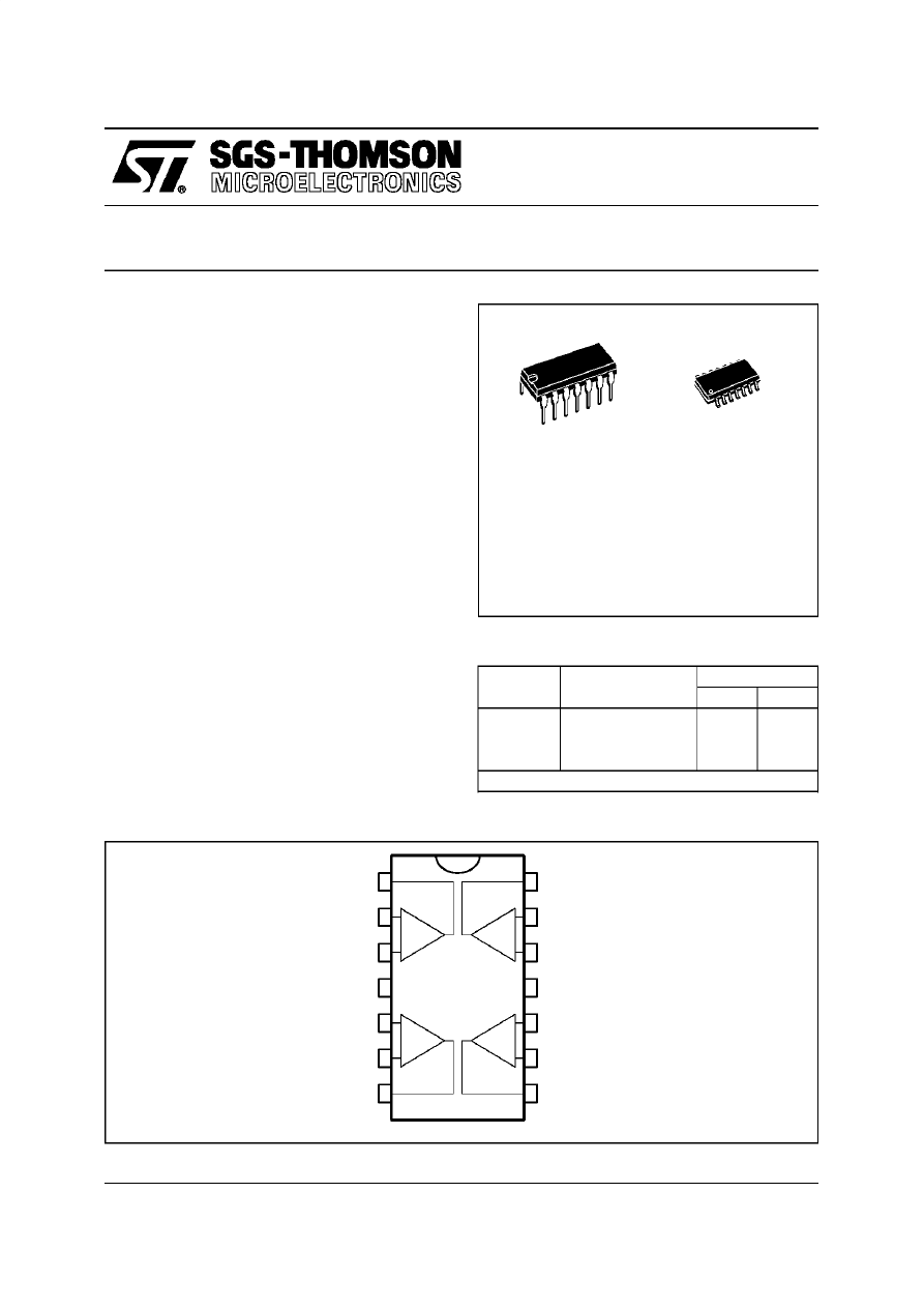
DESCRIPTION
These circuits consist of four independent, high
gain, internally frequency compensated operational
amplifiers . They operate from a single power supply
over a wide range of voltages. Operation from split
power supplies is also possible and the low power
supply current drain is independent of the magni-
tude of the power supply voltage.
Inve rting Input 2
Non-inve rting Input 2
Non-inve rting Input 1
CC
V
-
CC
V
1
2
3
4
8
5
6
7
9
10
11
12
13
14
+
Output 3
Output 4
Non-inve rting Input 4
Inve rting Input 4
Non-inve rting Input 3
Inve rting Input 3
-
+
-
+
-
+
-
+
Output 1
Inve rting Input 1
Output 2
PIN CONNECTIONS (top view)
ORDER CODES
Part
Number
Temperature
Range
Package
N
D
LM124
-55
o
C, +125
o
C
•
•
LM224
-40
o
C, +105
o
C
•
•
LM324
0
o
C, +70
o
C
•
•
Example : LM224N
N
DIP14
(Plastic Package)
D
SO14
(Plastic Micropackage)
LOW POWER QUAD OPERATIONAL AMPLIFIERS
LM124
LM224 - LM324
November 1997
1/13
ABSOLUTE MAXIMUM RATINGS
Symbol
Parameter
LM124
LM224
LM324
Unit
V
cc
Supply Voltage
±
16 or 32
V
V
i
Input Voltage
-0.3 to +32
V
V
id
Differential Input Voltage - (*)
+32
+32
+32
V
P
tot
Power Dissipation
N Suffix
D Suffix
500
-
500
400
500
400
mW
mW
-
Output Short-circuit Duration - (note 1)
Infinite
I
in
Input Current – (note 6)
50
50
50
mA
T
oper
Operating Free Air Temperature Range
-55 to +125
-40 to +105
0 to +70
o
C
T
stg
Storage Temperature Range
-65 to +150
-65 to +150
-65 to +150
o
C
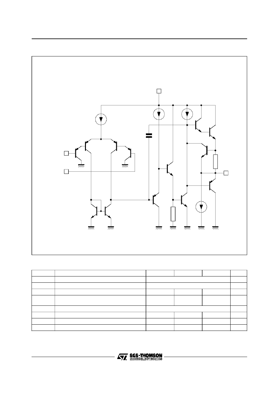
6
µ
A
4
µ
A
10 0
µ
A
Q2
Q3
Q4
Q1
Inve rting
inpu t
Non-inve rting
inpu t
Q8
Q9
Q10
Q1 1
Q12
5 0
µ
A
Q1 3
Outp ut
Q7
Q6
Q5
R
S C
V
CC
C
C
GND
SCHEMATIC DIAGRAM (1/4 LM124)
LM124 - LM224 - LM324
2/13
ELECTRICAL CHARACTERISTICS
V
CC
+
= +5V, V
CC
–
= Ground, V
O
= 1.4V, T
amb
= +25
o
C (unless otherwise specified)
Symbol
Parameter
LM124 - LM224 - LM324
Unit
Min.
Typ.
Max.
V
io
Input Offset Voltage (note 3)
T
amb
= +25
o
C
LM324
T
min.
≤
T
amb
≤
T
max
.
LM324
2
5
7
7
9
mV
I
io
Input Offset Current
T
amb
= +25
o
C
T
min.
≤
T
amb
≤
T
max
.
2
30
100
nA
I
ib
Input Bias Current (note 2)
T
amb
= +25
o
C
T
min.
≤
T
amb
≤
T
max
.
20
150
300
nA
A
vd
Large Signal Voltage Gain
(V
CC
+
= +15V, R
L
= 2k
Ω
, V
O
= 1.4V to 11.4V)
T
amb
= +25
o
C
T
min.
≤
T
amb
≤
T
max
.
50
25
100
V/mV
SVR
Supply Voltage Rejection Ratio (R
S
≤
10k
Ω
)
(V
CC
+
= 5V to 30V)
T
amb
= +25
o
C
T
min.
≤
T
amb
≤
T
max
.
65
65
110
dB
I
CC
Supply Current, all Amp, no load
T
amb
= +25
o
C
V
CC
= +5V
V
CC
= +30V
T
min.
≤
T
amb
≤
T
max
.
V
CC
= +5V
V
CC
= +30V
0.7
1.5
0.8
1.5
1.2
3
1.2
3
mA
V
icm
Input Common Mode Voltage Range
(V
CC
= +30V) - (note 4)
T
amb
= +25
o
C
T
min.
≤
T
amb
≤
T
max.
0
0
V
CC
-1.5
V
CC
-2
V
CMR
Common-mode Rejection Ratio (R
S
≤
10k
Ω
)
T
amb
= +25
o
C
T
min.
≤
T
amb
≤
T
max
70
60
80
dB
I
source
Output Current Source (V
id
= +1V)
V
CC
= +15V, V
o
= +2V
20
40
70
mA
I
sink
Output Sink Current (V
id
= -1V)
V
CC
= +15V, V
o
= +2V
V
CC
= +15V, V
o
= +0.2V
10
12
20
50
mA
µ
A
LM124 - LM224 - LM324
3/13
ELECTRICAL CHARACTERISTICS (continued)
Symbol
Parameter
LM124 - LM224 - LM324
Unit
Min.
Typ.
Max.
V
OH
High Level Output Voltage
(V
CC
= +30V)
T
amb
= +25
o
C
R
L
= 2k
Ω
T
min
.
≤
T
amb
≤
T
max
.
T
amb
= +25
o
C
R
L
= 10k
Ω
T
min
.
≤
T
amb
≤
T
max
.
(V
CC
= +5V, R
L
= 2k
Ω)
T
amb
= +25
o
C
T
min
.
≤
T
amb
≤
T
max
.
26
26
27
27
3.5
3
27
28
V
V
OL
Low Level Output Voltage (R
L
= 10k
Ω
)
T
amb
= +25
o
C
T
min
.
≤
T
amb
≤
T
max
.
5
20
20
mV
SR
Slew Rate
V
CC
= 15V, V
I
= 0.5 to 3V, R
L
= 2k
Ω
, C
L
= 100pF,
unity gain)
0.4
V/
µ
s
GBP
Gain Bandwidth Product
V
CC
= 30V, f = 100kHz, V
in
= 10mV
R
L
= 2k
Ω
, C
L
= 100pF
1.3
MHz
THD
Total Harmonic Distortion
f = 1kHz, A
V
= 20dB, R
L
= 2k
Ω
, V
O
= 2V
pp
C
L
= 100pF, V
CC
= 30V
0.015
%
e
n
Equivalent Input Noise Voltage
f = 1kHz, R
s
= 100
Ω
, V
CC
= 30V
40
nV
√
Hz
DV
io
Input Offset Voltage Drift
7
30
µ
V/
o
C
DI
IO
Input Offset Current Drift
10
200
pA/
o
C
V
O
1/V
O
2
Channel Separation (note 5)
1kHz
≤
f
≤
20kHz
120
dB
Notes :
1. Shor t -cir cui t s f rom t he out put t o V
C C
can cause excessi ve heat i ng if V
C C
> 15V. T he maxi mum out put cur rent
is appr oxi mat el y 40mA i ndependent of the magni t ude of V
C C
. D estr ucti ve di ssipat i on can r es ult f r om simul ta-
neous short -cir cuit on al l ampli f iers.
2. The di r ect ion of the i nput cur rent is out of t he IC . Thi s cur r ent is essenti al l y constant, i ndependent of the st ate
of the out put so no l oadi ng change exists on the i nput l i nes.
3. V
o
= 1. 4V , R
s
= 0
Ω,
5V < V
CC
+
< 30V , 0 < V
ic
< V
C C
+
- 1.5V
4. The i nput common- mode vol t age of eit her i nput si gnal volt age shoul d not be allow ed to go negat i ve by mor e
than 0.3V . T he upper end of the common- mode vol tage r ange i s V
C C
+
- 1.5V , but eit her or bot h i nput s can go
to + 32V w i thout damage.
5. Due t o the proxi mit y of ex ternal component s insure t hat coupl ing i s not ori gi nat ing vi a str ay capaci t ance be-
tw een these ext ernal par t s. T hi s t ypi call y can be detect ed as t his t ype of capaci tance i ncreases at higher f re-
quences.
6. This input cur rent onl y exi sts w hen t he volt age at any of t he i nput leads is dr iven negat ive. It i s due t o t he
coll ect or - base juncti on of t he i nput PN P transistor becomi ng forw ar d biased and ther eby act ing as input di-
odes clamps. I n addit i on to thi s di ode act i on, there i s al so N PN par asit i c act ion on the I C chip. t hi s t ransi st or
acti on can cause t he output vol t ages of the Op- amps t o go t o the V
CC
volt age l evel (or to ground f or a l arge
over dri ve) f or t he ti me dur at ion t han an input i s dr iven negati ve.
This i s not destr uct i ve and nor mal out put wi l l set up again f or i nput vol tage higher t han - 0.3V.
LM124 - LM224 - LM324
4/13
-55-35-15 5 25 45 65 85 105 125
AMBIENT TEMPERATURE ( C)
24
21
18
15
9
12
6
3
0
INPUT BIAS CURRENT
ve rs us AMBIENT TEMPERATURE
IB (nA)
SUPPLY
CURRENT
(mA)
S UPPLY CURRENT
0
10
20
30
Ta mb = -55 C
VCC
mA
ID
-
+
Tamb = 0 C to +125 C
POS ITIVE S UPP LY VOLTAGE (V)
4
3
2
1
LM124 - LM224 - LM324
5/13
LM124 - LM224 - LM324
6/13
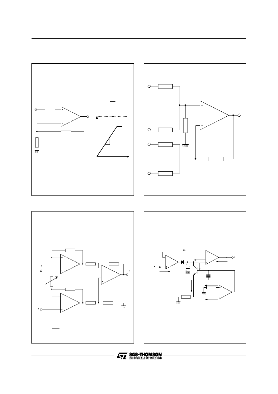
TYPICAL SINGLE - SUPPLY APPLICATIONS
1/4
LM124
~
0
2V
PP
R
10k
Ω
L
C
o
e
o
R
6.2k
Ω
B
R
100k
Ω
f
R1
10k
Ω
C
I
e
I
V
CC
R2
100k
Ω
C1
10
µ
F
R3
100k
Ω
A = -
R
R1
V
f
(as shown A = -10)
V
AC COUPLED INVERTING AMPLIFIER
1/4
LM124
~
0
2V
P P
R
10k
Ω
L
C
o
e
o
R
6.2k
Ω
B
C1
0.1
µ
F
e
I
V
CC
(a s s hown A = 11)
V
A = 1 +
R2
R1
V
R1
100k
Ω
R2
1M
Ω
C
I
R3
1M
Ω
R4
100k
Ω
R5
100k
Ω
C2
10
µ
F
AC COUPLED NON-INVERTING AMPLIFIER
LM124 - LM224 - LM324
7/13
R1
10k
Ω
R2
1M
Ω
1/4
LM124
10k
Ω
e
I
e
O
+5V
e
O
(V)
(mV)
0
A
V
= 1 +
R2
R1
(As shown
= 101)
A
V
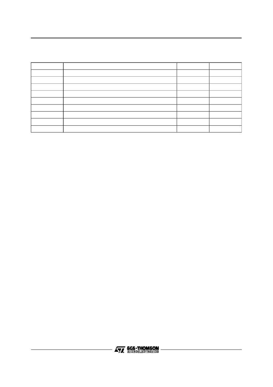
NON-INVERTING DC GAIN
1/4
LM124
e
O
e
4
e
3
e
2
e
1
100k
Ω
100k
Ω
100k
Ω
100k
Ω
100k
Ω
100k
Ω
e
o
= e
1
+ e
2
- e
3
- e
4
where (e
1
+ e
2
)
≥
(e
3
+ e
4
)
to keep e
o
≥
0V
DC SUMMING AMPLIFIER
1/4
LM124
R3
100k
Ω
e
O
1/4
LM124
R1
100k
Ω
e
1
1/4
LM124
R7
100k
Ω
R6
100k
Ω
R5
100k
Ω
e
2
R2
2k
Ω
Gain adjust
R4
100k
Ω
if R
1
= R
5
and R
3
= R
4
= R
6
= R
7
e
o
=
[ 1
+
2R
1
R
2
]
(
e
2
−
e
1
)
As shown e
o
= 101 (e
2
- e
1
).
HIGH INPUT Z ADJUSTABLE GAIN DC
INSTRUMENTATION AMPLIFIER
TYPICAL SINGLE - SUPPLY APPLICATIONS
1/4
LM124
1/4
LM124
I
B
2N 929
0.001
µ
F
I
B
3R
3M
Ω
I
B
Input current
compensation
e
o
I
B
e
I
1/4
LM124
Z
o
Z
I
C
1
µ
F
2I
B
R
1M
Ω
2I
B
* Polycarbonate or polyethylene
*
LOW DRIFT PEAK DETECTOR
LM124 - LM224 - LM324
8/13
1/4
LM124
1/4
LM124
R3
10k
Ω
1/4
LM124
e
1
e
O
R8
100k
Ω
R7
100k
Ω
C3
10
µ
F
V
CC
R5
470k
Ω
C2
330pF
R4
10M
Ω
R6
470k
Ω
R1
100k
Ω
C1
330pF
F
O
= 1kHz
Q = 50
A
V
= 100 (40dB)
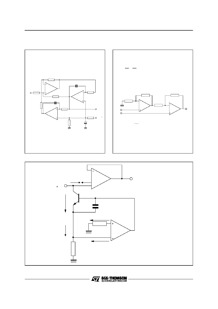
ACTIVER BANDPASS FILTER
1/4
LM124
1/4
LM124
R1
100k
Ω
R2
100k
Ω
R4
100k
Ω
R3
100k
Ω
+V2
+V1
V
o
e
o
(
1
+
R
4
R
3
) (
e
2
−
e
1
)
As shown e
o
= (e
2
- e
1
)
For
R
1
R
2
=
R
4
R
3
(CMRR depends on this resistor ratio match)
HIGH INPUT Z, DC DIFFERENTIAL AMPLIFIER
1/4
LM124
1/4
LM124
I
B
2N 929
0.001
µ
F
I
B
3M
Ω
I
B
e
o
I
I
e
I
I
B
I
B
Aux. amplifier for input
current compensation
1.5M
Ω
USING SYMMETRICAL AMPLIFIERS TO REDUCE INPUT CURRENT (GENERAL CONCEPT)
TYPICAL SINGLE - SUPPLY APPLICATIONS
LM124 - LM224 - LM324
9/13

.
LARGE VOLTAGE GAIN : 100dB
.
VERY LOW SUPPLY CURRENT/AMPLI :
375
µ
A
.
LOW INPUT BIAS CURRENT : 20nA
.
LOW INPUT OFFSET VOLTAGE : 2mV
.
LOW INPUT OFFSET CURRENT : 2nA
.
WIDE POWER SUPPLY RANGE :
SINGLE SUPPLY : +3V to +30V
DUAL SUPPLIES :
±
1.5V to
±
15V
** Standard Linear Ics Macromodels, 1993.
** CONNECTIONS :
* 1 INVERTING INPUT
* 2 NON-INVERTING INPUT
* 3 OUTPUT
* 4 POSITIVE POWER SUPPLY
* 5 NEGATIVE POWER SUPPLY
.SUBCKT LM124 1 3 2 4 5 (analog)
**********************************************************
.MODEL MDTH D IS=1E-8 KF=3.104131E-15
CJO=10F
* INPUT STAGE
CIP 2 5 1.000000E-12
CIN 1 5 1.000000E-12
EIP 10 5 2 5 1
EIN 16 5 1 5 1
RIP 10 11 2.600000E+01
RIN 15 16 2.600000E+01
RIS 11 15 2.003862E+02
DIP 11 12 MDTH 400E-12
DIN 15 14 MDTH 400E-12
VOFP 12 13 DC 0
VOFN 13 14 DC 0
IPOL 13 5 1.000000E-05
CPS 11 15 3.783376E-09
DINN 17 13 MDTH 400E-12
VIN 17 5 0.000000e+00
DINR 15 18 MDTH 400E-12
VIP 4 18 2.000000E+00
FCP 4 5 VOFP 3.400000E+01
FCN 5 4 VOFN 3.400000E+01
FIBP 2 5 VOFN 2.000000E-03
FIBN 5 1 VOFP 2.000000E-03
* AMPLIFYING STAGE
FIP 5 19 VOFP 3.600000E+02
FIN 5 19 VOFN 3.600000E+02
RG1 19 5 3.652997E+06
RG2 19 4 3.652997E+06
CC 19 5 6.000000E-09
DOPM 19 22 MDTH 400E-12
DONM 21 19 MDTH 400E-12
HOPM 22 28 VOUT 7.500000E+03
VIPM 28 4 1.500000E+02
HONM 21 27 VOUT 7.500000E+03
VINM 5 27 1.500000E+02
EOUT 26 23 19 5 1
VOUT 23 5 0
ROUT 26 3 20
COUT 3 5 1.000000E-12
DOP 19 25 MDTH 400E-12
VOP 4 25 2.242230E+00
DON 24 19 MDTH 400E-12
VON 24 5 7.922301E-01
.ENDS
Applies to : LM124-LM224-LM324
LM124 - LM224 - LM324
10/13
ELECTRICAL CHARACTERISTICS
V
CC
+
= +5V, V
CC
-
= 0V, T
amb
= 25
o
C (unless otherwise specified)
Symbol
Conditions
Value
Unit
V
io
0
mV
A
vd
R
L
= 2k
Ω
100
V/mV
I
CC
No load, per operator
350
µ
A
V
icm
-15 to +13.5
V
V
OH
R
L
= 2k
Ω
(V
CC
+
= 15V)
+13.5
V
V
OL
RL = 10k
Ω
5
mV
I
OS
V
O
= +2V, V
CC
= +15V
+40
mA
GBP
R
L
= 2k
Ω,
C
L
= 100pF
1.3
MHz
SR
R
L
= 2k
Ω,
C
L
= 100pF
0.4
V/
µ
s
LM124 - LM224 - LM324
11/13
PM-DIP14.EPS
PACKAGE MECHANICAL DATA
14 PINS - PL ASTIC DIP
Dimensions
Millimeters
Inches
Min.
Typ.
Max.
Min.
Typ.
Max.
a1
0.51
0.020
B
1.39
1.65
0.055
0.065
b
0.5
0.020
b1
0.25
0.010
D
20
0.787
E
8.5
0.335
e
2.54
0.100
e3
15.24
0.600
F
7.1
0.280
i
5.1
0.201
L
3.3
0.130
Z
1.27
2.54
0.050
0.100
DIP14.TBL
LM124 - LM224 - LM324
12/13
PM-SO14.EPS
PACKAGE MECHANICAL DATA
14 PINS - PL ASTIC MICROPACKAGE (SO)
Dimensions
Millimeters
Inches
Min.
Typ.
Max.
Min.
Typ.
Max.
A
1.75
0.069
a1
0.1
0.2
0.004
0.008
a2
1.6
0.063
b
0.35
0.46
0.014
0.018
b1
0.19
0.25
0.007
0.010
C
0.5
0.020
c1
45
o
(typ.)
D
8.55
8.75
0.336
0.334
E
5.8
6.2
0.228
0.244
e
1.27
0.050
e3
7.62
0.300
F
3.8
4.0
0.150
0.157
G
4.6
5.3
0.181
0.208
L
0.5
1.27
0.020
0.050
M
0.68
0.027
S
8
o
(max.)
SO14.TBL
Information furnished is believed to be accurate and reliable. However, SGS-THOMSON Microelectronics assumes no responsi-
bility for the consequences of use of such information nor for any infringement of patents or other rights of third parties which
may result from its use. No license is granted by implication or otherwise under any patent or patent rights of SGS-THOMSON
Microelectronics. Specifications mentioned in this publication are subject to change without noti ce. This publ ication supersedes
and replaces all information previously supplied. SGS-THOMSON Microelectronics products are not authorized for use as critical
componen ts in life support devices or systems without express written approval of SGS-THOMSON Microelectronics.
1997 SGS-THOMSON Microelectronics – Printed in Italy – All Rights Reserved
SGS-THOMSON Microelectronics GROUP OF COMPANIES
Australia - Brazil - Canada - China - France - Germany - Hong Kong - Italy - Japan - Korea - Malaysia - Malta - Morocco
The Netherlands - Singapore - Spain - Sweden - Switzerland - Taiwan - Thailand - United Kingdom - U.S.A.
ORDER
CODE
:
LM124 - LM224 - LM324
13/13
Wyszukiwarka
Podobne podstrony:
lm324
elebot linia LM324
lm324
LM224 LM324 LM2902
więcej podobnych podstron