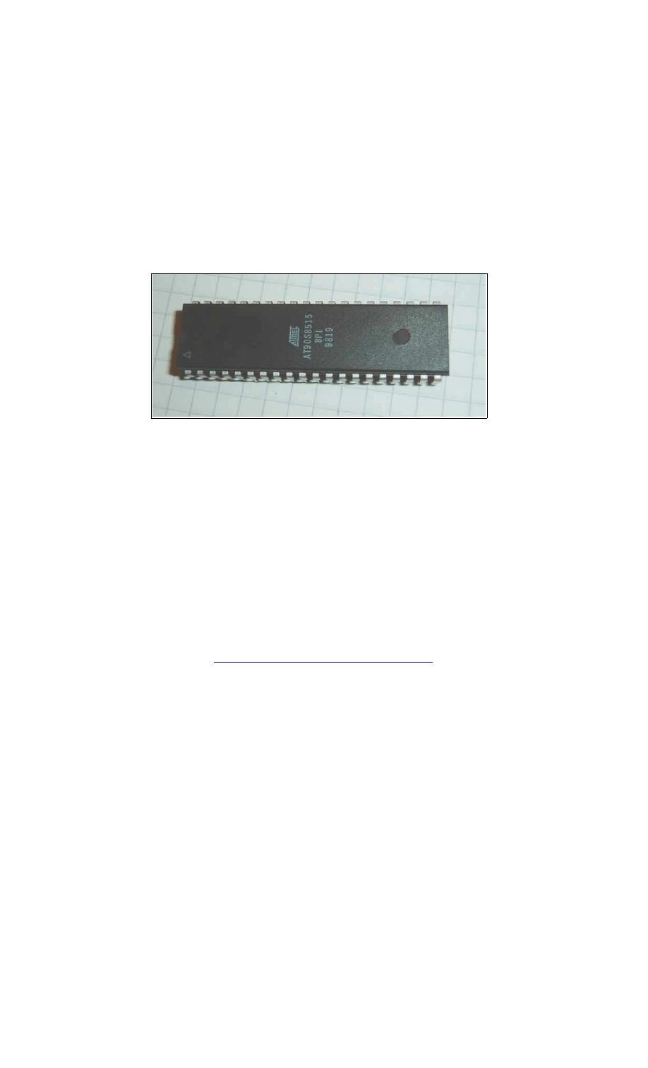
Beginners Introduction to the
Assembly Language of
ATMELAVRMicroprocessors
by
Gerhard Schmidt
http://www.avrasmtutorial.net
December 2003


Avr-Asm-Tutorial
1
http://www.avr-asm-tutorial.net
Content
Why learning Assembler?..........................................................................................................................1
Short and easy.......................................................................................................................................1
Fast and quick........................................................................................................................................1
Assembler is easy to learn.....................................................................................................................1
AT90Sxxxx are ideal for learning assembler........................................................................................1
Test it!....................................................................................................................................................1
Hardware for AVRAssemblerProgramming...........................................................................................2
The ISPInterface of the AVRprocessor family...................................................................................2
Programmer for the PCParallelPort....................................................................................................2
Experimental board with a AT90S2313................................................................................................3
Readytouse commercial programming boards for the AVRfamily...................................................4
Tools for AVR assembly programing........................................................................................................5
The editor..............................................................................................................................................5
The assembler........................................................................................................................................6
Programming the chips..........................................................................................................................7
Simulation in the studio.........................................................................................................................7
Register......................................................................................................................................................9
What is a register?.................................................................................................................................9
Different registers................................................................................................................................10
Pointerregister....................................................................................................................................10
Recommendation for the use of registers............................................................................................11
Ports.........................................................................................................................................................12
What is a Port?....................................................................................................................................12
Details of relevant ports in the AVR...................................................................................................13
The status register as the most used port.............................................................................................13
Port details...........................................................................................................................................14
SRAM..................................................................................................................................................15
Using SRAM in AVR assembler language.........................................................................................15
What is SRAM?...................................................................................................................................15
For what purposes can I use SRAM?..................................................................................................15
How to use SRAM?.............................................................................................................................15
Use of SRAM as stack.........................................................................................................................16
Defining SRAM as stack................................................................................................................16
Use of the stack...............................................................................................................................17
Bugs with the stack operation.........................................................................................................17
Jumping and Branching............................................................................................................................19
Controlling sequential execution of the program................................................................................19
What happens during a reset?.........................................................................................................19
Linear program execution and branches..............................................................................................20
Timing during program execution.......................................................................................................20
Macros and program execution...........................................................................................................21
Subroutines..........................................................................................................................................21
Interrupts and program execution........................................................................................................23
Calculations..............................................................................................................................................25
Number systems in assembler.............................................................................................................25
Positive whole numbers (bytes, words, etc.)..................................................................................25
Signed numbers (integers)..............................................................................................................25
Binary Coded Digits, BCD.............................................................................................................25
Packed BCDs..................................................................................................................................26
Numbers in ASCIIformat..............................................................................................................26
Bit manipulations................................................................................................................................26
Shift and rotate....................................................................................................................................27
Adding, subtracting and comparing....................................................................................................28
Format conversion for numbers...........................................................................................................29
Multiplication......................................................................................................................................30
Decimal multiplication...................................................................................................................30
Binary multiplication......................................................................................................................30

Avr-Asm-Tutorial
2
http://www.avr-asm-tutorial.net
AVRAssembler program...............................................................................................................31
Binary rotation................................................................................................................................32
Multiplication in the studio.............................................................................................................32
Division...............................................................................................................................................34
Decimal division.............................................................................................................................34
Binary division...............................................................................................................................34
Program steps during division........................................................................................................35
Division in the simulator................................................................................................................35
Number conversion.............................................................................................................................37
Decimal Fractions................................................................................................................................37
Linear conversions..........................................................................................................................37
Example 1: 8bitADconverter with fixed decimal output............................................................38
Example 2: 10bitADconverter with fixed decimal output..........................................................40
Annex.......................................................................................................................................................41
Commands sorted by function.............................................................................................................41
Command list in alphabetic order.......................................................................................................43
Assembler directives.......................................................................................................................43
Commands......................................................................................................................................43
Port details...........................................................................................................................................45
StatusRegister, Accumulator flags................................................................................................45
Stackpointer....................................................................................................................................45
SRAM and External Interrupt control............................................................................................45
External Interrupt Control...............................................................................................................46
Timer Interrupt Control..................................................................................................................46
Timer/Counter 0..............................................................................................................................47
Timer/Counter 1..............................................................................................................................48
WatchdogTimer.............................................................................................................................49
EEPROM........................................................................................................................................49
Serial Peripheral Interface SPI........................................................................................................50
UART.............................................................................................................................................51
Analog Comparator........................................................................................................................51
I/O Ports..........................................................................................................................................52
Ports, alphabetic order.........................................................................................................................52
List of abbreviations............................................................................................................................53

Avr-Asm-Tutorial
1
http://www.avr-asm-tutorial.net
Why learning Assembler?
Assembler or other languages, that is the question. Why should I learn another language, if I already
learned other programming languages? The best argument: while you live in France you are able to get
through by speaking english, but you will never feel at home then, and life remains complicated. You can
get through with this, but it is rather inappropriate. If things need a hurry, you should use the country's
language.
Short and easy
Assembler commands translate one by one to executed machine commands. The processor needs only to
execute what you want it to do and what is necessary to perform the task. No extra loops and unnecessary
features blow up the generated code. If your program storage is short and limited and you have to optimize
your program to fit into memory, assembler is choice 1. Shorter programs are easier to debug, every step
makes sense.
Fast and quick
Because only necessary code steps are executed, assembly programs are as fast as possible. The
duration of every step is known. Time critical applications, like time measurements without a hardware
timer, that should perform excellent, must be written in assembler. If you have more time and don't mind if
your chip remains 99% in a wait state type of operation, you can choose any language you want.
Assembler is easy to learn
It is not true that assmbly language is more complicated or not as easy to understand than other
languages. Learning assembly language for whatever hardware type brings you to understand the basic
concepts of any other assembly language dialect. Adding other dialects later is easy. The first assembly
code does not look very attractive, with every 100 additional lines programmed it looks better. Perfect
programs require some thousand lines of code of exercise, and optimization requires lots of work. As
some features are hardware-dependant optimal code requires some familiarity with the hardware concept
and the dialect. The first steps are hard in any language. After some weeks of programming you will laugh
if you go through your first code. Some assembler commands need some monthes of experience.
AT90Sxxxx are ideal for learning assembler
Assembler programs are a little bit silly: the chip executes anything you tell it to do, and does not ask you if
you are sure overwriting this and that. All protections must be programmed by you, the chip does anything
like it is told. No window warns you, unless you programmed it before.
Basic design errors are as complicated to debug like in any other computer language. But: testing
programs on ATMEL chips is very easy. If it does not do what you expect it to do, you can easily add some
diagnostic lines to the code, reprogram the chip and test it. Bye, bye to you EPROM programmers, to the
UV lamps used to erase your test program, to you pins that don't fit into the socket after having them
removed some douzend times.
Changes are now programmed fast, compiled in no time, and either simulated in the studio or checked in-
circuit. No pin is removed, and no UV lamp gives up just in the moment when you had your excellent idea
about that bug.
Test it!
Be patient doing your first steps! If you are familiar with another (high-level) language: forget it for the first
time. Behind every assembler language there is a certain hardware concept. Most of the special features
of other computer languages don't make any sense in assembler.
The first five commands are not easy to learn, then your learning speed rises fast. After you had your first
lines: grab the instruction set list and lay back in the bathtub, wondering what all the other commands are
like.
Don't try to program a mega-machine to start with. This does not make sense in any computer language,
and just produces frustration.
Comment your subroutines and store them in a special directory, if debugged: you will need them again in
a short time.
Have success!
Avr-Asm-Tutorial
2
http://www.avr-asm-tutorial.net
Hardware for AVRAssemblerProgramming
Learning assembler requires some simple hardware equipment to test your programs, and see if it works
in practice.
This section shows two easy schematics that enable you to homebrew the required hardware and gives
you the necessary hints on the required background. This hardware really is easy to build. I know nothing
easier than that to test your first software steps. If you like to make more experiments, leave some more
space for future extensions on your experimental board.
If you don't like the smell of soldering, you can buy a ready-to-use board, too. The available boards are
characterised in this section below.
The ISPInterface of the AVRprocessor family
Before going into practice, we have to learn a few essentials on the serial programming mode of the AVR
family. No, you don't need three different voltages to program and read an AVR flash memory. No, you
don't need another microprocessor to program the AVRs. No, you don't need 10 I/O lines to tell the chip
what you like it to do. And you don't even have to remove the AVR from your experimental board, before
programming it. It's even easier than that.
All this is done by a build-in interface in the AVR chip, that enables you to write and read the content of the
program flash and the built-in-EEPROM. This interface works serially and needs three signal lines:
•
SCK: A clock signal that shifts the bits to be written to the memory into an internal shift register, and
that shifts out the bits to be read from another internal shift register,
•
MOSI: The data signal that sends the bits to be written to the AVR,
•
MISO: The data signal that receives the bits read from the AVR.
These three signal pins are internally connected to the programming machine only if you change the
RESET (sometimes also called RST or restart) pin to zero. Otherwise, during normal operation of the AVR,
these pins are programmable I/O lines like all the others.
If you like to use these pins for other purposes during normal operation, and for in-
system-programming, you'll have to take care, that these two purposes do not
conflict. Usually you then decouple these by resistors or by use of a multiplexer.
What is necessary in your case, depends from your use of the pins in the normal
operation mode. You're lucky, if you can use them for in- system-programming
exclusively.
Not necessary, but recommendable for in-system-programming is, that you supply
the programming hardware out of the supply voltage of your system. That makes it
easy, and requires two additional lines between the programmer and the AVR
board. GND is the common ground, VTG (target voltage) the supply voltage
(usually 5.0 volts). This adds up to 6 lines between the programmer and the AVR
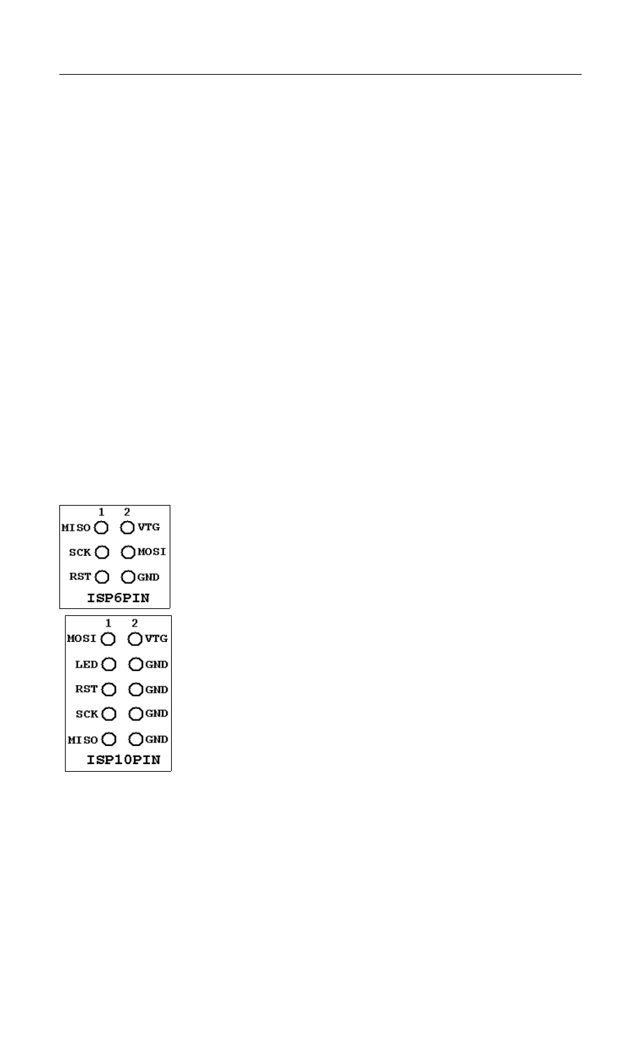
board. The resulting ISP6 connection is, as defined by AMEL, is shown on the left.
Standards always have alternative standards, that were used earlier. This is the
technical basis that constitutes the adaptor industry. In our case the alternative
standard was designed as ISP10 and was used on the STK200 board. It's still a
very widespread standard, and even the STK500 is still equipped with it. ISP10
has an additional signal to drive a red LED. This LED signals that the programmer
is doing his job. A good idea. Just connect the LED to a resistor and clamp it the
positive supply voltage.
Programmer for the PCParallelPort
Now, heat up your soldering iron and build up your programmer. It is a quite easy schematic and works
with standard parts from your well-sorted experiments box.
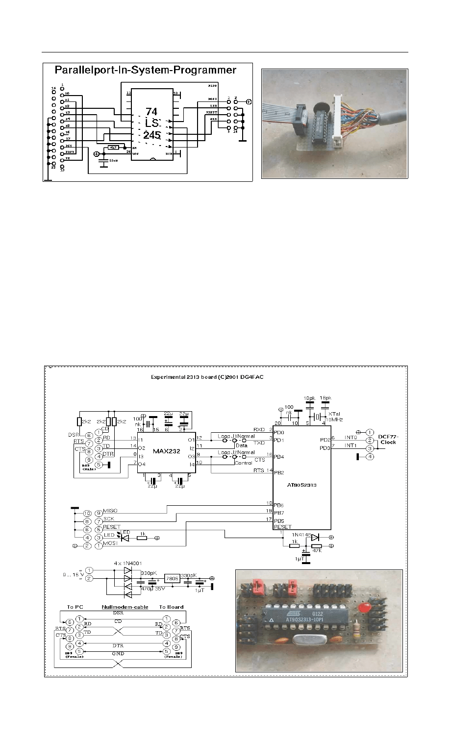
Yes, that's all you need to program an AVR. The 25-pin plug goes into the parallel port of your PC, the 10-
pin-ISP goes to your AVR experimental board. If your box doesn't have a 74LS245, you can also use a
74HC245 or a 74LS244/74HC244 (by changing some pins and signals). If you use HC, don't forget to tie
unused inputs either to GND or the supply voltage, otherwise the buffers might produce extra noise by
capacitive switching.
Avr-Asm-Tutorial
3
http://www.avr-asm-tutorial.net
The necessary program algorithm is done by the ISP software, that is available from ATMEL's software
download page.
Experimental board with a AT90S2313
For test purposes we use a AT90S2313 on an experimental board. The schematic shows
•
a small voltage supply for connection to an AC transformer and a voltage regulator 5V/1A,
•
a XTAL clock generator (here with a 10 Mcs/s, all other frequencies below the maximum for the 2313
will also work),
•
the necessary parts for a safe reset during supply voltage switching,
•
the ISP-Programming-Interface (here with a ISP10PIN-connector).
So that's what you need to start with. Connect other peripheral add-ons to the numerous free I/O pins of
the 2313.
The easiest output device can be a LED, connected via a resistor to the positive supply voltage. With that,
you can start writing your first assembler program switching the LED on and off.

Avr-Asm-Tutorial
4
http://www.avr-asm-tutorial.net
Readytouse commercial programming boards for the
AVRfamily
If you do not like homebrewed hardware, and if have some extra money left that you don't know what to do
with, you can buy a commercial programming board. Easy to get is the STK500 (e.g. from ATMEL. It has
the following hardware:
•
Sockets for programming most of the AVR types,
•
serial und parallel programming,
•
ISP6PIN- and ISP10PIN-connector for external In-System-Programming,
•
programmable oscillator frequency and suplly voltages,
•
plug-in switches and LEDs,
•
a plugged RS232C-connector (UART),
•
a serial Flash-EEPROM,
•
access to all ports via a 10-pin connector.
Experiments can start with the also supplied AT90S8515. The board is connected to the PC using a serial
port (COMx) and is controlled by later versions of AVR studio, available from ATMEL's webpage. This
covers all hardware requirements that the beginner might have.
Avr-Asm-Tutorial
5
http://www.avr-asm-tutorial.net
Tools for AVR assembly programing
This section provides informations about the necessary tools that are used to program AVRs with the
STK200 board. Programming with the STK500 is very different and shown in more detail in the Studio
section. Note that the older software for the STK200 is not supported any more.
Four basic programs are necessary for assembly programming. These tools are:
•
the editor,
•
the assembler program,
•
the chip programing interface, and
•
the simulator.
The necessary software tools are ©ATMEL and available on the webpage of ATMEL for download. The
screenshots here are ©ATMEL. It should be mentioned that there are different versions of the software
and some of the screenshots are subject to change with the used version. Some windows or menues look
different in different versions. The basic functions are mainly unchanged. Refer to the programer's
handbook, this page just provides an overview for the beginner's first steps and is not written for the
assembly programing expert.
The editor
Assembler programs are written with a editor. The editor just has to be able to create and edit ASCII text
files. So, basically, any simple editor does it. I recommend the use of a more advanced editor, either
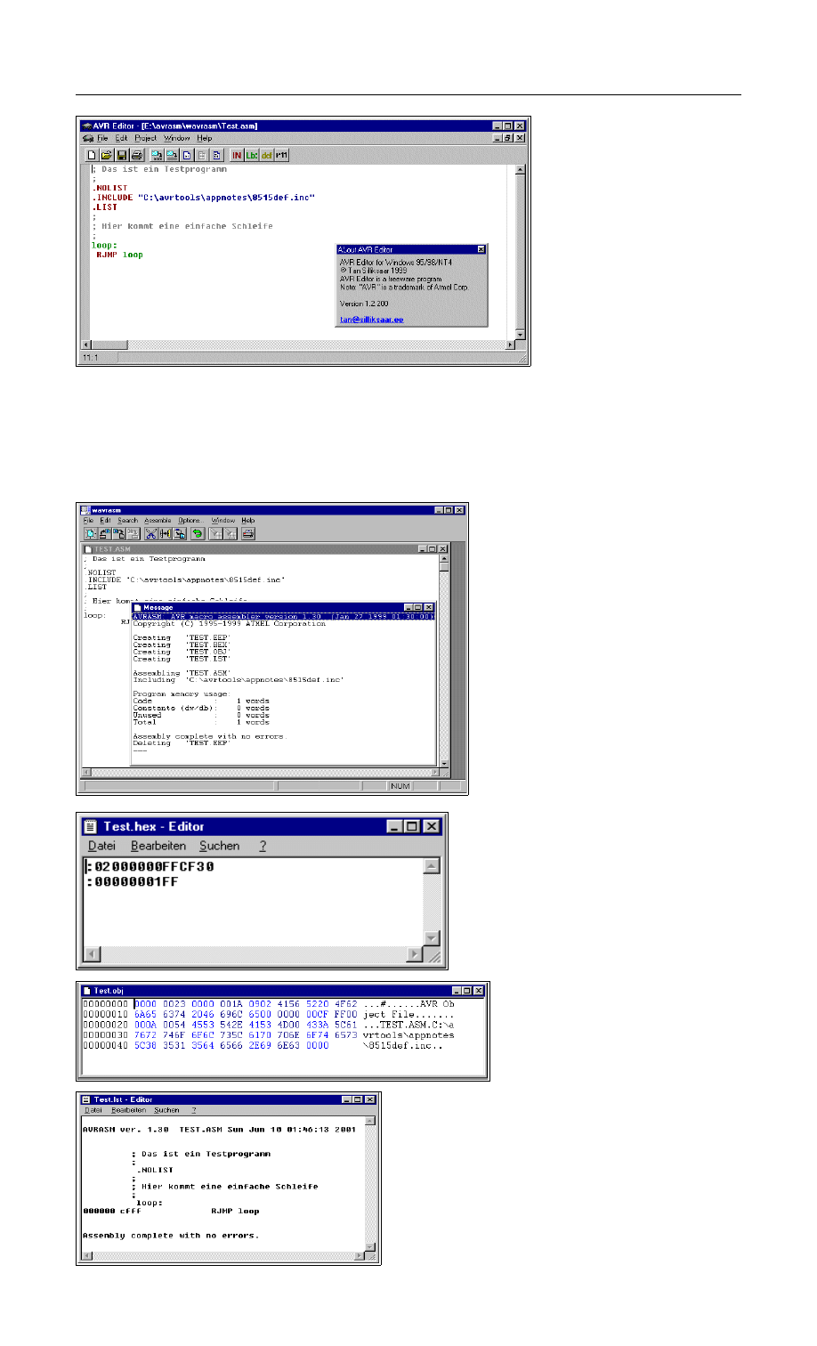
WAVRASM©ATMEL or the editor written by Tan Silliksaar (screenshot see below).
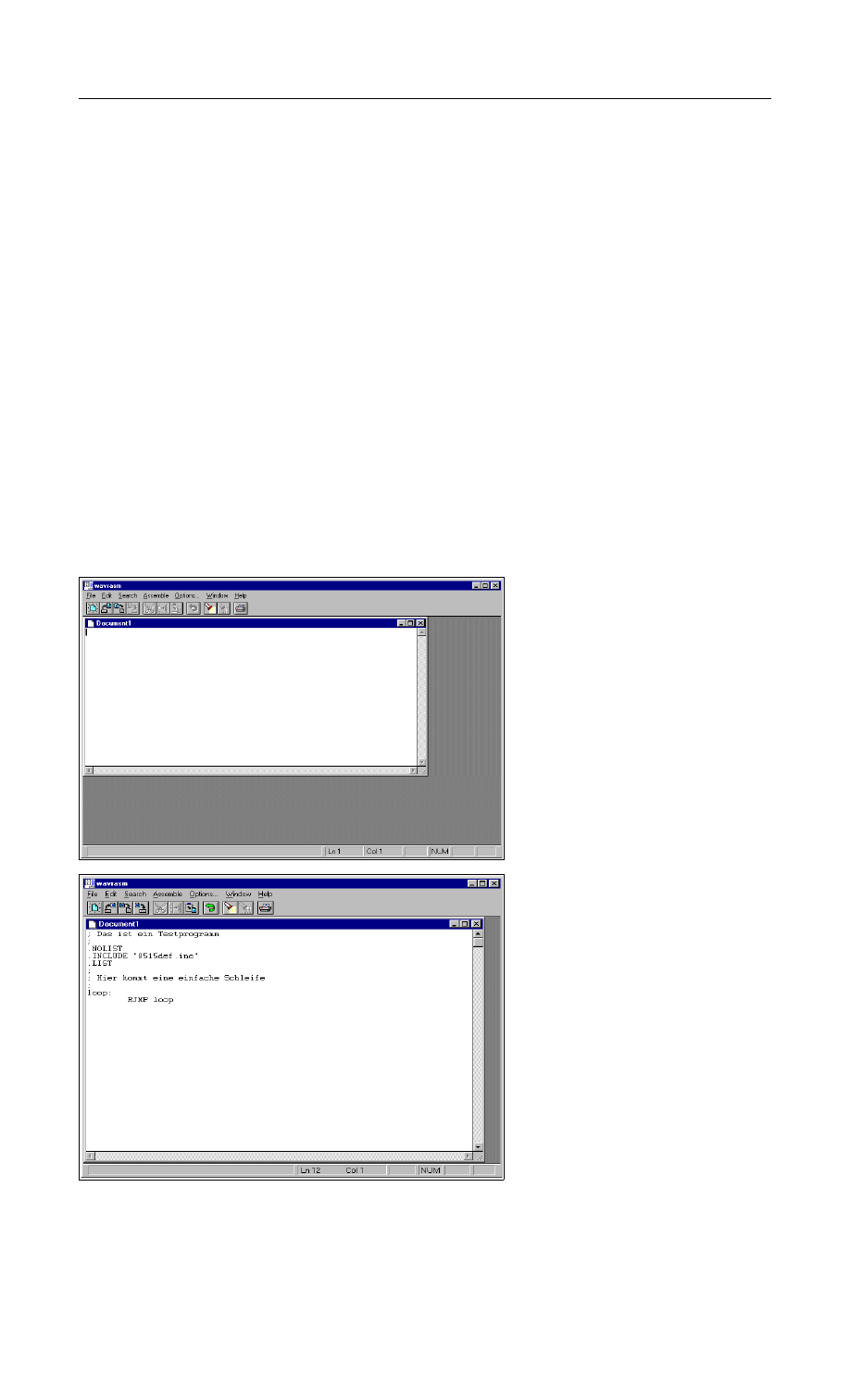
An assembly program written with
WAVRASM© goes like this. Just install
WAVRASM© and start the program:
Now we type in our directives and
assembly commands in the WAVRASM
editor window, together with some
comments (starting with ;). That should
look like this:
Now store the program text, named to something.asm into a dedicated directory, using the file menue. The
assembly program is complete now.
If you like editing a little more in a sophisticated manner you can use the excellent editor written by Tan
Silliksaar. This editor tools is designed for AVRs and available for free from Tan's webpage. In this editor
our program looks like this:
Avr-Asm-Tutorial
6
http://www.avr-asm-tutorial.net
The editor recognizes com-
mands automatically and uses
different colors (syntax high-
lighting) to signal user constants
and typing errors in those
commands (in black). Storing
the code in an .asm file provides
nearly the same text file.
The assembler
Now we have to translate this code to a machine-oriented form well understood by the AVR chip. Doing
this is called assembling, which means collecting the right command words. If you use WAVRASM© just
click assemble on the menue. The result is shown here:
The assembler reports the complete
translation with no errors. If errors occur
these are notified. Assembling resulted in
one word of code which resulted from the
command we used. Assembling our single
asm-text file now has produced four other
files (not all apply here).
The first of these four new files,
TEST.EEP, holds the content that should
be written to the EEPROM of the AVR.
This is not very interesting in our case,
because we didn't program any content
for the EEPROM. The assembler has
therefore deleted this file when he
completed the assembly run.
The second file, TEST.HEX, is more relevant
because this file holds the commands later
programmed into the AVR chip. This file
looks like this.
The hex numbers are written in a special
ASCII form, together with adress informations
and a checksum for each line. This form is
called Intel-hex-format, and it is very old. The
form is well understood by the programing
software.
The third file, TEST.OBJ, will be
introduced later, this file is needed to
simulate an AVR. Its format is
hexadecimal and defined by ATMEL.
Using a hex-editor its content looks
like this. Attention: This file format is
not compatible with the programer software, don't use
this file to program the AVR (a very common error when
starting).
The fourth file, TEST.LST, is a text file. Display its
content with a simple editor. The following results.
The program with all its adresses, comands and error
messages are displayed in a readable form. You will
need that file in some cases to debug errors.
Avr-Asm-Tutorial
7
http://www.avr-asm-tutorial.net
Programming the chips
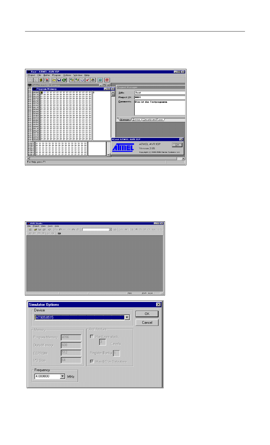
To program our hex code to the AVR ATMEL has written the ISP software package. (Not that this software
is not supported and distributed any more.) We start the ISP software and load the hex file that we just
generated (applying menue item LOAD PROGRAM). That looks like this:
Applying menue item
PROGRAM will burn our
code in the chip's program
store. There are a number
of preconditions necessary
for this step (the correct
parallel port has to be
selected, the programming
adapter
must
be
connected, the chip must
be on board the adapter,
the power supply must be
on, etc.).
Besides the ATMEL-ISP
and the programming
boards other programming
boards or adapters could
be used, together with the
appropriate programming software. Some of these alternatives are available on the internet.
Simulation in the studio
In some cases self-written assembly code, even assembled without errors, does not exactly do what it
should do when burned into the chip. Testing the software on the chip could be complicated, esp. if you
have a minimum hardware and no opportunity to display interim results or debugging signals. In these
cases the studio from ATMEL provides ideal opportunities for debugging. Testing the software or parts of it
is possible, the program could be tested step-by-step displaying results.
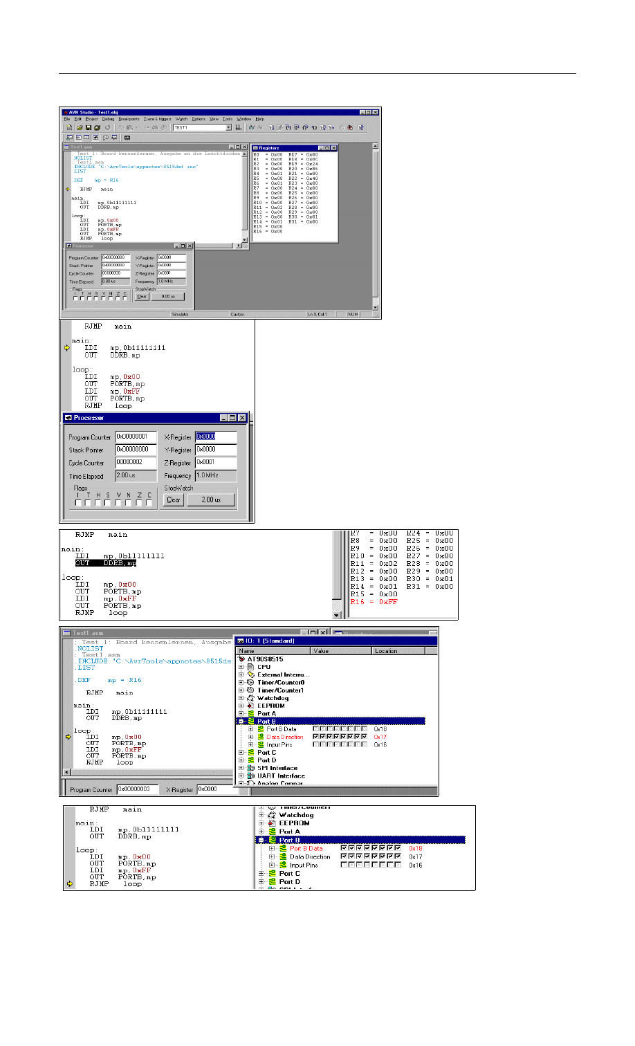
The studio is started and looks like
this.
First we open a file (menue item FILE
OPEN). We demonstrate this using
the tutorial file test1.asm, because
there are some more commands and
action that in our single-command
program above.
Open the file TEST1.OBJ that results
by assembling TEST1.asm. You are
asked which options you like to use (if
not, you can change these using the
menue item SIMULATOR OPTIONS).
The following options will be selected:
In the device selection section we
select the desired chip type. The
correct frequency should be selected
if you like to simulate correct timings.
In order to view the content of some registers and what the processor's status is we select VIEW
PROCESSOR and REGISTERS. The display should now look like this.
Avr-Asm-Tutorial
8
http://www.avr-asm-tutorial.net
The processor window displays all
values like the command counter, the
flags and the timing information (here:
1 MHz clock). The stop watch can be
used to measure the necessary time
for going through routines etc.
Now we start the program execution. We use the single step
opportunity (TRACE INTO or F11). Using GO would result in
continous exection and not much would be seen due to the high
speed of simulation. After the first executed step the processor
window should look like this.
The program counter is at step 1, the cycle counter at 2 (RJMP
needed two cycles). At 1 MHz clock two microseconds have
been wasted, the flags and pointer registers are not changed.
The source text window displays a pointer on the next command
that will be executed.
Pressing F11 again executes the next command, register mp
(=R16) will be set to 0xFF. Now the register window should
highlite this change.
Register R16's new
value is displayed in
red letters. We can
change the value of a
register at any time to
test what happens
then.
Now step 3 is
executed, output to the
direction register of Port B.
To display this we open a
new I/O view window and
select Port B. The display
should look like this.
The Data Direction
Register in the I/O-view
window of Port B now
shows the new value. The
values could be changed
manually, if desired, pin by
pin.
The next two steps
are simulated using
F11. They are not
displayed here.
Setting the output
ports to one with
the command LDI
mp,0xFF and OUT PORTB,mp results in the following picture in the I/O view. Now the output port bits are
all one, the I/O view shows this.
That is our short trip through the simulator software world. The simulator is capable to much more, so it
should be applied extensively in cases of design errors. Visit the different menue items, there is much
more than showed here.

Avr-Asm-Tutorial
9
http://www.avr-asm-tutorial.net
Register
What is a register?
Registers are special storages with 8 bits capacity and they look like this:
Bit 7
Bit 6
Bit 5
Bit 4
Bit 3
Bit 2
Bit 1
Bit 0
Note the numeration of these bits: the least significant bit starts with zero (2
0
= 1).
A register can either store numbers from 0 to 255 (positive number, no negative values), or numbers from
-128 to +127 (whole number with a sign bit in bit 7), or a value representing an ASCII-coded character
(e.g. 'A'), or just eight single bits that do not have something to do with each other (e.g. for eight single
flags used to signal eight different yes/no decisions).
The special character of registers, compared to other storage sites, is that
•
they can be used directly in assembler commands,
•
operations with their content require only a single command word,
•
they are connected directly to the central processing unit called the accumulator,
•
they are source and target for calculations.
There are 32 registers in an AVR. They are originally named R0 to R31, but you can choose to name them
to more meaningful names using an assembler directive. An example:
.DEF MyPreferredRegister = R16
Assembler directives always start with a dot in column 1 of the text. Instructions do NEVER start in column
1, they are always preceeded by a Tab- or blank character!
Note that assembler directives like this are only meaningful for the assembler but do not produce any code
that is executable in the AVR target chip. Instead of using the register name R16 we can now use our own
name MyPreferredRegister, if we want to use R16 within a command. So we write a little bit more text each
time we use this register, but we have an association what might be the content of this register.
Using the command line
LDI
MyPreferredRegister, 150
which means: load the number 150 immediately to the register R16, LoaD Immediate. This loads a fixed
value or a constant to that register. Following the assembly or translation of this code the program storage
written to the AVR chip looks like this:
000000 E906
The load command code as well as the target register (R16) as well as the value of the constant (150) is
part of the hex value E906, even if you don't see this directly. Don't be afraid: you don't have to remember
this coding because the assembler knows how to translate all this to yield E906.
Within one command two different registers can play a role. The easiest command of this type is the copy
command MOV. It copies the content of one register to another register. Like this:
.DEF MyPreferredRegister = R16
.DEF AnotherRegister = R15
LDI MyPreferredRegister, 150
MOV AnotherRegister, MyPreferredRegister
The first two lines of this monster program are directives that define the new names of the registers R16
and R15 for the assembler. Again, these lines do not produce any code for the AVR. The command lines
with LDI and MOV produce code:
000000 E906
000001 2F01
The commands write 150 into register R16 and copy its content to the target register R15. IMPORTANT
NOTE:
The first register is always the target register where the result is written to!
(This is unfortunately different from what one expects or from how we speak. It is a simple convention that
was once defined that way to confuse the beginners learning assembler. That is why assembler is that
complicated.)

Avr-Asm-Tutorial
10
http://www.avr-asm-tutorial.net
Different registers
The beginner might want to write the above commands like this:
.DEF AnotherRegister = R15
LDI AnotherRegister, 150
And: you lost. Only the registers from R16 to R31 load a constant immediately with the LDI command, R0
to R15 don't do that. This restriction is not very fine, but could not be avoided during construction of the
command set for the AVRs.
There is one exception from that rule: setting a register to Zero. This command
CLR MyPreferredRegister
is valid for all registers.
Besides the LDI command you will find this register class restriction with the following additional
commands:
•
ANDI Rx,K ; Bit-And of register Rx with a constant value K,
•
CBR Rx,M ; Clear all bits in register Rx that are set to one within the constant mask value M,
•
CPI Rx,K ; Compare the content of the register Rx with a constant value K,
•
SBCI Rx,K ; Subtract the constant K and the current value of the carry flag from the content of
register Rx and store the result in register Rx,
•
SBR Rx,M ; Set all bits in register Rx to one, that are one in the constant mask M,
•
SER Rx ; Set all bits in register Rx to one (equal to LDI Rx,255),
•
SUBI Rx,K ; Subtract the constant K from the content of register Rx and store the result in register
Rx.
In all these commands the register must be between R16 and R31! If you plan to use these commands
you should select one of these registers for that operation. It is easier to program. This is an additional
reason why you should use the directive to define a register's name, because you can easier change the
registers location afterwards.
Pointerregister
A very special extra role is defined for the register pairs R26:R27, R28:R29 and R30:R31. The role is so
important that these pairs have extra names in AVR assembler: X, Y and Z. These pairs are 16-bit pointer
registers, able to point to adresses with max. 16-bit into SRAM locations (X, Y or Z) or into locations in
program memory (Z).
The lower byte of the 16-bit-adress is located in the lower register, the higher byte in the upper register.
Both parts have their own names, e.g. the higher byte of Z is named ZH (=R31), the lower Byte is ZL
(=R30). These names are defined in the standard header file for the chips. Dividing these 16-bit-pointer-
names into two different bytes is done like follows:
.EQU Adress = RAMEND ; RAMEND is the highest 16-bit adress in SRAM
LDI YH,HIGH(Adress) ; Set the MSB
LDI YL,LOW(Adress) ; Set the LSB
Accesses via pointers are programmed with specially designed commands. Read access is named LD
(LoaD), write access named ST (STore), e.g. with the X-pointer:
Pointer
Sequence
Examples
X
Read/Write from adress X, don't change the pointer
LD R1,X or ST X,R1
X+
Read/Write from/to adress X and increment the pointer afterwards by
one
LD R1,X+ or ST X+,R1
-X
Decrement the pointer by one and read/write from/to the new adress
afterwards
LD R1,-X or ST -X,R1
Similiarly you can use Y and Z for that purpose.
There is only one command for the read access to the program storage. It is defined for the pointer pair Z
and it is named LPM (Load from Program Memory). The command copies the byte at adress Z in the
program memory to the register R0. As the program memory is organised word-wise (one command on
one adress consists of 16 bits or two bytes or one word) the least significant bit selects the lower or higher
byte (0=lower byte, 1= higher byte). Because of this the original adress must be multiplied by 2 and access
is limited to 15-bit or 32 kB program memory. Like this:

Avr-Asm-Tutorial
11
http://www.avr-asm-tutorial.net
LDI ZH,HIGH(2*Adress)
LDI ZL,LOW(2*Adress)
LPM
Following this command the adress must be incremented to point to the next byte in program memory. As
this is used very often a special pointer incrementation command has been defined to do this:
ADIW ZL,1
LPM
ADIW means ADd Immediate Word and a maximum of 63 can be added this way. Note that the assembler
expects the lower of the pointer register pair ZL as first parameter. This is somewhat confusing as addition
is done as 16-bit- operation.
The complement command, subtracting a constant value of between 0 and 63 from a 16-bit pointer
register is named SBIW, Subtract Immediate Word. (SuBtract Immediate Word). ADIW and SBIW are
possible for the pointer register pairs X, Y and Z and for the register pair R25:R24, that does not have an
extra name and does not allow access to SRAM or program memory locations. R25:R24 is ideal for
handling 16-bit values.
How to insert that table of values in the program memory? This is done with the assembler directives .DB
and .DW. With that you can insert bytewise or wordwise lists of values. Bytewise organised lists look like
this:
.DB 123,45,67,89 ; a list of four bytes
.DB "This is a text. " ; a list of byte characters
You should always place an even number of bytes on each single line. Otherwise the assembler will add a
zero byte at the end, which might be unwanted.
The similiar list of words looks like this:
.DW 12345,6789 ; a list of two words
Instead of constants you can also place labels (jump targets) on that list, like that:
Label1:
[ ... here are some commands ... ]
Label2:
[ ... here are some more commands ... ]
Table:
.DW Label1,Label2 ; a wordwise list of labels
Labels ALWAYS start in column 1!. Note that reading the labels with LPM first yields the lower byte of the
word.
A very special application for the pointer registers is the access to the registers themselves. The registers
are located in the first 32 bytes of the chip's adress space (at adress 0x0000 to 0x001F). This access is
only meaningful if you have to copy the register's content to SRAM or EEPROM or read these values from
there back into the registers. More common for the use of pointers is the access to tables with fixed values
in the program memory space. Here is, as an example, a table with 10 different 16-bit values, where the
fifth table value is read to R25:R24:
MyTable:
.DW 0x1234,0x2345,0x3456,0x4568,0x5678 ; The table values, wordwise
.DW 0x6789,0x789A,0x89AB,0x9ABC,0xABCD ; organised
Read5: LDI ZH,HIGH(MyTable*2) ; Adress of table to pointer Z
LDI ZL,LOW(MyTable*2) ; multiplied by 2 for bytewise access
ADIW ZL,10 ; Point to fifth value in table
LPM ; Read least significant byte from program memory
MOV R24,R0 ; Copy LSB to 16-bit register
ADIW ZL,1 ; Point to MSB in program memory
LPM ; Read MSB of table value
MOV R25,R0 ; Copy MSB to 16-bit register
This is only an example. You can calculate the table adress in Z from some input value, leading to the
respective table values. Tables can be organised byte- or character-wise, too.
Recommendation for the use of registers
•
Define names for registers with the .DEF directive, never use them with their direct name Rx.
•
If you need pointer access reserve R26 to R31 for that purpose.
•
16-bit-counter are best located R25:R24.
•
If you need to read from the program memory, e.g. fixed tables, reserve Z (R31:R30) and R0 for that
purpose.
•
If you plan to have access to single bits within certain registers (e.g. for testing flags), use R16 to
R23 for that purpose.

Avr-Asm-Tutorial
12
http://www.avr-asm-tutorial.net
Ports
What is a Port?
Ports in the AVR are gates from the central processing unit to internal and external hard- and software
components. The CPU communicates with these components, reads from them or writes to them, e.g. to
the timers or the parallel ports. The most used port is the flag register, where results of previous operations
are written to and branch conditions are read from.
There are 64 different ports, which are not physically available in all different AVR types. Depending on the
storage space and other internal hardware the different ports are either available and accessable or not.
Which of these ports can be used is listed in the data sheets for the processor type.
Ports have a fixed address, over which the CPU communicates. The address is independent from the type
of AVR. So e.g. the port adress of port B is always 0x18 (0x stands for hexadecimal notation). You don't
have to remember these port adresses, they have convenient aliases. These names are defined in the
include files (header files) for the different AVR types, that are provided from the producer. The include
files have a line defining port B's address as follows:
.EQU PORTB, 0x18
So we just have to remember the name of port B, not its location in the I/O space of the chip. The include
file 8515def.inc is involved by the assembler directive
.INCLUDE "C:\Somewhere\8515def.inc"
and the registers of the 8515 are all defined then and easily accessable.
Ports usually are organised as 8-bit numbers, but can also hold up to 8 single bits that don't have much to
do with each other. If these single bits have a meaning they have their own name associated in the include
file, e.g. to enable manipulation of a single bit. Due to that name convention you don't have to remember
these bit positions. These names are defined in the data sheets and are given in the include file, too. They
are provided here in the port tables.
As an example the MCU General Control Register, called MCUCR, consists of a number of single control
bits that control the general property of the chip (see the description in MCUCR in detail). It is a port, fully
packed with 8 control bits with their own names (ISC00, ISC01, ...). Those who want to send their AVR to
a deep sleep need to know from the data sheet how to set the respective bits. Like this:
.DEF MyPreferredRegister = R16
LDI MyPreferredRegister, 0b00100000
OUT MCUCR, MyPreferredRegister
SLEEP
The Out command brings the content of my preferred register, a Sleep-Enable-Bit called SE, to the port
MCUCR and sets the AVR immediately to sleep, if there is a SLEEP instruction executed. As all the other
bits of MCUCR are also set by the above instructions and the Sleep Mode bit SM was set to zero, a mode
called half-sleep will result: no further command execution will be performed but the chip still reacts to
timer and other hardware interrupts. These external events interrupt the big sleep of the CPU if they feel
they should notify the CPU.
Reading a port's content is in most cases possible using the IN command. The following sequence
.DEF MyPreferredRegister = R16
IN MyPreferredRegister, MCUCR
reads the bits in port MCUCR to the register. As many ports have undefined and unused bits in certain
ports, these bits always read back as zeros.
More often than reading all 8 bits of a port one must react to a certain status of a port. In that case we don't
need to read the whole port and isolate the relevant bit. Certain commands provide an opportunity to
execute commands depending on the level of a certain bit (see the JUMP section). Setting or clearing
certain bits of a port is also possible without reading and writing the other bits in the port. The two
commands are SBI (Set Bit I/o) and CBI (Clear Bit I/o). Execution is like this:
.EQU ActiveBit=0 ; The bit that is to be changed
SBI PortB, ActiveBit ; The bit will be set to one
CBI PortB, Activebit ; The bit will be cleared to zero
These two instructions have a limitation: only ports with an adress smaller than 0x20 can be handled, ports
above cannot be accessed that way.
For the more exotic programmer: the ports can be accessed using SRAM access commands, e.g. ST and
LD. Just add 0x20 to the port's adress (the first 32 addresses are the registers!) and access the port that
way. Like demonstrated here:
.DEF MyPreferredRegister = R16
LDI ZH,HIGH(PORTB+32)

Avr-Asm-Tutorial
13
http://www.avr-asm-tutorial.net
LDI ZL,LOW(PORTB+32)
LD MyPreferredRegister,Z
That only makes sense in certain cases, but it is possible. It is the reason why the first address location of
the SRAM is always 0x60.
Details of relevant ports in the AVR
The following table holds the most used ports. Not all ports are listed here, some of the MEGA and
AT90S4434/8535 types are skipped. If in doubt see the original reference.
Component
Portname
Port-Register
Accumulator
SREG
Status Register
Stack
SPL/SPH
Stackpointer
External SRAM/External Interrupt MCUCR
MCU General Control Register
External Interrupt
GIMSK
Interrupt Mask Register
GIFR
Interrupt Flag Register
Timer Interrupt
TIMSK
Timer Interrupt Mask Register
TIFR
Timer Interrupt Flag Register
Timer 0
TCCR0
Timer/Counter 0 Control Register
TCNT0
Timer/Counter 0
Timer 1
TCCR1A
Timer/Counter Control Register 1 A
TCCR1B
Timer/Counter Control Register 1 B
TCNT1
Timer/Counter 1
OCR1A
Output Compare Register 1 A
OCR1B
Output Compare Register 1 B
ICR1L/H
Input Capture Register
Watchdog Timer
WDTCR
Watchdog Timer Control Register
EEPROM
EEAR
EEPROM Adress Register
EEDR
EEPROM Data Register
EECR
EEPROM Control Register
SPI
SPCR
Serial Peripheral Control Register
SPSR
Serial Peripheral Status Register
SPDR
Serial Peripheral Data Register
UART
UDR
UART Data Register
USR
UART Status Register
UCR
UART Control Register
UBRR
UART Baud Rate Register
Analog Comparator
ACSR
Analog Comparator Control and Status Register
I/O-Ports
PORTx
Port Output Register
DDRx
Port Direction Register
PINx
Port Input Register
The status register as the most used port
By far the most often used port is the status register with its 8 bits. Usually access to this port is only by
automatic setting and clearing bits by the CPU or accumulator, some access is by reading or branching on
certain bits in that port, in a few cases it is possible to manipulate these bits directly (using the assembler
command SEx or CLx, where x is the bit abbreviation). Most of these bits are set or cleared by the
accumulator through bit-test, compare- or calculation-operations. The following list has all assembler
commands that set or clear status bits depending on the result of the execution.

Avr-Asm-Tutorial
14
http://www.avr-asm-tutorial.net
Bit
Calculation
Logic
Compare
Bits
Shift
Other
Z
ADD, ADC, ADIW, DEC,
INC, SUB, SUBI, SBC,
SBCI, SBIW
AND, ANDI, OR,
ORI, EOR, COM,
NEG, SBR, CBR
CP, CPC,
CPI
BCLR Z,
BSET Z, CLZ,
SEZ, TST
ASR, LSL,
LSR, ROL,
ROR
CLR
C
ADD, ADC, ADIW, SUB,
SUBI, SBC, SBCI, SBIW
COM, NEG
CP, CPC,
CPI
BCLR C,
BSET C,
CLC, SEC
ASR, LSL,
LSR, ROL,
ROR
-
N
ADD, ADC, ADIW, DEC,
INC, SUB, SUBI, SBC,
SBCI, SBIW
AND, ANDI, OR,
ORI, EOR, COM,
NEG, SBR, CBR
CP, CPC,
CPI
BCLR N,
BSET N, CLN,
SEN, TST
ASR, LSL,
LSR, ROL,
ROR
CLR
V
ADD, ADC, ADIW, DEC,
INC, SUB, SUBI, SBC,
SBCI, SBIW
AND, ANDI, OR,
ORI, EOR, COM,
NEG, SBR, CBR
CP, CPC,
CPI
BCLR V,
BSET V, CLV,
SEV, TST
ASR, LSL,
LSR, ROL,
ROR
CLR
S
SBIW
-
-
BCLR S,
BSET S, CLS,
SES
-
-
H
ADD, ADC, SUB, SUBI,
SBC, SBCI
NEG
CP, CPC,
CPI
BCLR H,
BSET H, CLH,
SEH
-
-
T
-
-
-
BCLR T,
BSET T, BST,
CLT, SET
-
-
I
-
-
-
BCLR I, BSET
I, CLI, SEI
-
RETI
Port details
Port details of the most common ports are shown in an extra table (see annex).
Avr-Asm-Tutorial
15
http://www.avr-asm-tutorial.net
SRAM
Using SRAM in AVR assembler language
Nearly all AT90S-AVR-type MCUs have static RAM (SRAM) on board (some don't). Only very simple
assembler programs can avoid using this memory space by putting all info into registers. If you run out of
registers you should be able to program the SRAM to utilize more space.
What is SRAM?
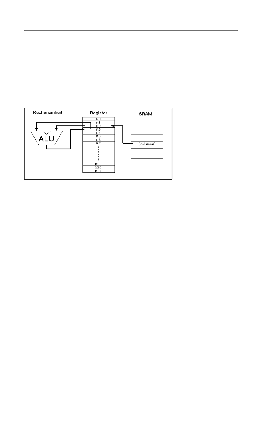
SRAM are memories that are not directly accessable to the central processing unit (Arithmetic and Logical
Unit ALU, sometimes called
accumulator) like the registers
are. If you access these
memory locations you usually
use a register as interim
storage. In the following
example a value in SRAM will
be copied to the register R2
(1st command), a calculation
with the value in R3 is made
and the result is written to R3
(command 2). After that this
value is written back to the
SRAM location (command 3,
not shown here).
So it is clear that operations with values stored in the SRAM are slower to perform than those using
registers alone. On the other hand: the smallest AVR type has 128 bytes of SRAM available, much more
than the 32 registers can hold.
The types from AT90S8515 upwards offer the additional opportunity to connect additional external RAM,
expanding the internal 512 bytes. From the assembler point-of-view, external SRAM is accessed like
internal SRAM. No extra commands must be used for that external SRAM.
For what purposes can I use SRAM?
Besides simple storage of values, SRAM offers additional opportunities for its use. Not only access with
fixed addresses is possible, but also the use of pointers, so that floating access to subsequent locations
can be programmed. This way you can build up ring buffers for interim storage of values or calculated
tables. This is not very often used with registers, because they are too few and prefer fixed access.
Even more relative is the access using an offset to a fixed starting address in one of the pointer registers.
In that case a fixed address is stored in a pointer register, a constant value is added to this address and
read/write access is made to that address with an offset. With that kind of access tables are better used.
The most relevant use for SRAM is the so-called stack. You can push values to that stack, be it the content
of a register, a return address prior to calling a subroutine, or the return address prior to an hardware-
triggered interrupt.
How to use SRAM?
To copy a value to a memory location in SRAM you have to define the address. The SRAM addresses you
can use reach from 0x0060 (hex notation) to the end of the physical SRAM on the chip (in the AT90S8515
the highest accessable internal SRAM location is 0x025F). With the command
STS 0x0060, R1
the content of register R1 is copied to the first SRAM location. With
LDS R1, 0x0060
the SRAM content at address 0x0060 is copied to the register. This is the direct access with an address
that has to be defined by the programmer.
Symbolic names can be used to avoid handling fixed addresses, that require a lot of work, if you later want
to change the structure of your data in the SRAM. These names are easier to handle than hex numbers, so
give that address a name like:
.EQU MyPreferredStorageCell = 0x0060

Avr-Asm-Tutorial
16
http://www.avr-asm-tutorial.net
STS MyPreferredStorageCell, R1
Yes, it isn't shorter, but easier to remember. Use whatever name that you find to be convenient.
Another kind of access to SRAM is the use of pointers. You need two registers for that purpose, that hold
the 16-bit address of the location. As we learned in the Pointer-Register-Division pointer registers are the
pairs X (XH:XL, R27:R26), Y (YH:YL, R29:R28) and Z (ZH:ZL, R31:R30). They allow access to the
location they point to directly (e.g. with ST X, R1), after prior decrementing the address by one (e.g. ST -X,
R1) or with subsequent incrementation of the address (e.g. ST X+, R1). A complete access to three cells
in a row looks like this:
.EQU MyPreferredStorageCell = 0x0060
.DEF MyPreferredRegister = R1
.DEF AnotherRegister = R2
.DEF AndAnotherRegister = R3
LDI XH, HIGH(MyPreferredStorageCell)
LDI XL, LOW(MyPreferredStorageCell)
LD MyPreferredRegister, X+
LD AnotherRegister, X+
LD AndAnotherRegister, X
Easy to operate, those pointers. And as easy as in other languages than assembler, that claim to be
easier to learn.
The third construction is a little bit more exotic and only experienced programmers use this. Let's assume
we very often in our program need to access three SRAM locations. Let's futher assume that we have a
spare pointer register pair, so we can afford to use it exclusively for our purpose. If we would use the
ST/LD instructions we always have to change the pointer if we access another location. Not very
convenient.
To avoid this, and to confuse the beginner, the access with offset was invented. During that access the
register value isn't changed. The address is calculated by temporarly adding the fixed offset. In the above
example the access to location 0x0062 would look like this. First, the pointer register is set to our central
location 0x0060:
.EQU MyPreferredStorageCell = 0x0060
.DEF MyPreferredRegister = R1
LDI YH, HIGH(MyPreferredStorageCell)
LDI YL, LOW(MyPreferredStorageCell)
Somewhere later in the program I'd like to access cell 0x0062:
STD Y+2, MyPreferredRegister
Note that 2 is not really added to Y, just temporarly. To confuse you further, this can only be done with the
Y- and Z-register-pair, not with the X-pointer!
The corresponding instruction for reading from SRAM with an offset
LDD MyPreferredRegister, Y+2
is also possible.
That's it with the SRAM, but wait: the most relevant use as stack is still to be learned.
Use of SRAM as stack
The most common use of SRAM is its use as stack. The stack is a tower of wooden blocks. Each
additional block goes onto the top of the tower, each recall of a value removes the upmost block from the
tower. This structure is called Last-In-First-Out (LIFO) or easier: the last to go on top will be the first
coming down.
Defining SRAM as stack
To use SRAM as stack requires the setting of the stack pointer first. The stack pointer is a 16-bit-pointer,
accessable like a port. The double register is named SPH:SPL. SPH holds the most significant address
byte, SPL the least significant. This is only true, if the AVR type has more than 256 byte SRAM. If not, SPH
is undefined and must not and cannot be used. We assume we have more than 256 bytes in the following
examples.
To construct the stack the stack pointer is loaded with the highest available SRAM address. (In our case
the tower grows downwards, towards lower addresses!).
.DEF MyPreferredRegister = R16
LDI MyPreferredRegister, HIGH(RAMEND) ; Upper byte
OUT SPH,MyPreferredRegister ; to stack pointer
LDI MyPreferredRegister, LOW(RAMEND) ; Lower byte
OUT SPL,MyPreferredRegister ; to stack pointer

Avr-Asm-Tutorial
17
http://www.avr-asm-tutorial.net
The value RAMEND is, of course, specific for the processor type. It is defined in the INCLUDE file for the
processor type. The file 8515def.inc has the line:
.equ RAMEND =$25F ; Last On-Chip SRAM Location
The file 8515def.inc is included with the assembler directive
.INCLUDE "C:\somewhere\8515def.inc"
at the beginning of our assembler source code.
So we defined the stack now, and we don't have to care about the stack pointer any more, because
manipulations of that pointer are automatic.
Use of the stack
Using the stack is easy. The content of registers are pushed onto the stack like this:
PUSH MyPreferredRegister ; Throw that value
Where that value goes to is totally uninteresting. That the stack pointer was decremented after that push,
we don't have to care. If we need the content again, we just add the following instruction:
POP MyPreferredRegister ; Read back the value
With POP we just get the value that was last pushed on top of the stack. Pushing and popping registers
makes sense, if
•
the content is again needed some lines of code later,
•
all registers are in use, and if
•
no other opportunity exists to store that value somewhere else.
If these conditions are not given, the use of the stack for saving registers is useless and just wastes
processor time.
More sense makes the use of the stack in subroutines, where you have to return to the program location
that called the routine. In that case the calling program code pushes the return address (the current
program counter value) onto the stack and jumps to the subroutine. After its execution the subroutine pops
the return address from the stack and loads it back into the program counter. Program execution is
continued exactly one instruction behind the call instruction:
RCALL Somewhat ; Jump to the label somewhat
[...] here we continue with the program.
Here the jump to the label somewhat somewhere in the program code,
Somewhat: ; this is the jump address
[...] Here we do something
[...] and we are finished and want to jump back to the calling location:
RET
During execution of the RCALL instruction the already incremented program counter, a 16-bit-address, is
pushed onto the stack, using two pushes. By reaching the RET instruction the content of the previous
program counter is reloaded with two pops and execution continues there.
You don't need to care about the address of the stack, where the counter is loaded to. This address is
automatically generated. Even if you call a subroutine within that subroutine the stack function is fine. This
just packs two return addresses on top of the stack, the nested subroutine removes the first one, the
calling subroutine the remaining one. As long as there is enough SRAM, everything is fine.
Servicing hardware interrupts isn't possible without the stack. Interrupts stop the normal exection of the
program, wherever the program currently is. After execution of a specific service routine as a reaction to
that interrupt program execution must return to the previous location, before the interrupt occurred. This
would not be possible if the stack is not able to store the return address.
The enormous advances of having a stack for interrupts are the reason, why even the smallest AVRs
without having SRAM have at least a very small hardware stack.
Bugs with the stack operation
For the beginner there are a lot of possible bugs, if you first learn to use stack.
Very clever is the use of the stack without first setting the stack pointer. Because this pointer is set to zero
at program start, the pointer points to register R0. Pushing a byte results in a write to that register,
overwriting its previous content. An additional push to the stack writes to 0xFFFF, an undefined position (if
you don't have external SRAM there). A RCALL and RET will return to a strange address in program
memory. Be sure: there is no warning, like a window popping up saying something like „Illegal Access to
Mem location xxxx“.

Avr-Asm-Tutorial
18
http://www.avr-asm-tutorial.net
Another opportunity to construct bugs is to forget to pop a previously pushed value, or popping a value
without pushing one first.
In a very few cases the stack overflows to below the first SRAM location. This happens in case of a never-
ending recursive call. After reaching the lowest SRAM location the next pushes write to the ports (0x005F
down to 0x0020), then to the registers (0x001F to 0x0000). Funny and unpredictable things happen with
the chip hardware, if this goes on. Avoid this bug, it can even destroy your hardware!

Avr-Asm-Tutorial
19
http://www.avr-asm-tutorial.net
Jumping and Branching
Here we discuss all commands that control the sequential execution of a program. It starts with the starting
sequence on power-up of the processor, jumps, interrupts, etc.
Controlling sequential execution of the program
What happens during a reset?
When the power supply of an AVR rises and the processor starts its work, the hardware triggers a reset
sequence. The counter for the program steps will be set to zero. At this address the execution always
starts. Here we have to have our first word of code. But not only during power-up this address is activated:
•
During an external reset on the reset pin a restart is executed.
•
If the Watchdog counter reaches its maximum count, a reset is initiated. A watchdog timer is an
internal clock that must be resetted from time to time by the program, otherwise it restarts the
processor.
•
You can call reset by a direct jump to that address (see the jump section below).
The third case is not a real reset, because the automatic resetting of register- and port-values to a well-
defined default value is not executed. So, forget that for now.
The second option, the watchdog reset, must first be enabled by the program. It is disabled by default.
Enabling requires write commands to the watchdog's port. Setting the watchdog counter back to zero
requires the execution of the command
WDR
to avoid a reset.
After execution of a reset, with setting registers and ports to default values, the code at address 0000 is
wordwise read to the execution part of the processor and is executed. During that execution the program
counter is already incremented by one and the next word of code is already read to the code fetch buffer
(Fetch during Execution). If the executed command does not require a jump to another location in the
program the next command is executed immediately. That is why the AVRs execute extremely fast, each
clock cycle executes one command (if no jumps occur).
The first command of an executable is always located at address 0000. To tell the compiler (assembler
program) that our source code starts now and here, a special directive can be placed at the beginning,
before the first code in the source is written:
.CSEG
.ORG 0000
The first directive lets the compiler switch to the code section. All following is translated as code and is
written to the program memory section of the processor. Another target segment would be the EEPROM
section of the chip, where you also can write bytes or words to.
.ESEG
The third segment is the SRAM section of the chip.
.DSEG
Other than with EEPROM content, that really goes to the EEPROM during programming of the chip, the
DSEG segment content is not programmed to the chip. It is only used for correct label calculation during
the assembly process.
The ORG directive above stands for origin and manipulates the address within the code segment, where
assembled words go to. As our program always starts at 0x0000 the CSEG/ORG directives are trivial, you
can skip these without getting into an error. We could start at 0x0100, but that makes no real sense as the
processor starts execution at 0000. If you want to place a table exactly to a certain location of the code
segment, you can use ORG. If you want to set a clear sign within your code, after first defining a lot of
other things with .DEF- and .EQU-directives, use the CSEG/ORG sequence, even though it might not be
necessary to do that.
As the first code word is always at address zero, this location is also called the reset vector. Following the
reset vector the next positions in the program space, addresses 0x0001, 0x0002 etc., are interrupt vectors.
These are the positions where the execution jumps to if an external or internal interrupt has been enabled
and occurs. These positions called vectors are specific for each processor type and depend on the internal
hardware available (see below). The commands to react to such an interrupt have to be placed to the
proper vector location. If you use interrupts, the first code, at the reset vector, must be a jump command, to
jump over the other vectors. Each interrupt vector must hold a jump command to the respective interrupt
service routine. The typical program sequence at the beginning is like follows:

Avr-Asm-Tutorial
20
http://www.avr-asm-tutorial.net
.CSEG
.ORG 0000
RJMP Start
RJMP IntServRout1
[...] here we place the other interrupt vector commands
[...] and here is a good place for the interrupt service routines themselves
Start: ; This here is the program start
[...] Here we place our main program
The command RJMP results in a jump to the label Start:, located some lines below. Remeber, labels
always start in column 1 of the source code and end with a :. Labels, that don't fulfil these conditions are
not taken for serious by many compiler. Missing labels result in an error message ("Undefined label"), and
compilation is interrupted.
Linear program execution and branches
Program execution is always linear, if nothing changes the sequential execution. These changes are the
execution of an interrupt or of branching instructions.
Branching is very often depending on some condition, conditioned branching. As an example we assume
we want to construct a 32-bit-counter using registers R1 to R4. The least significant byte in R1 is
incremented by one. If the register overflows during that operation (255 + 1 = 0), we have to increment R2
similiarly. If R2 overflows, we have to increment R3, and so on.
Incrementation by one is done with the instruction INC. If an overflow occurs during that execution of
INC R1 the zero bit in the status register is set to one (the result of the operation is zero). The carry bit in
the status register, usually set by overflows, is not changed during an INC. This is not to confuse the
beginner, but carry is used for other purposes instead. The Zero-Bit or Zero-flag in this case is enough to
detect an overflow. If no overflow occurs we can just leave the counting sequence.
If the Zero-bit is set, we must execute additional incrementation of the other registers.To confuse the
beginner the branching command, that we have to use, is not named BRNZ but BRNE (BRanch if Not
Equal). A matter of taste ...
The whole count sequence of the 32-bit-counter should then look like this:
INC R1
BRNE GoOn32
INC R2
BRNE GoOn32
INC R3
BRNE GoOn32
INC R4
GoOn32:
So that's about it. An easy thing. The opposite condition to BRNE is BREQ or BRanch EQual.
Which of the status bits, also called processor flags, are changed during execution of a command is listed
in instruction code tables, see the List of Instructions. Similiarly to the Zero-bit you can use the other status
bits like that:
BRCC label/BRCS label; Carry-flag 0 oder 1
BRSH label; Equal or greater
BRLO label; Smaller
BRMI label; Minus
BRPL label; Plus
BRGE label; Greater or equal (with sign bit)
BRLT label; Smaller (with sign bit)
BRHC label/BRHS label; Half overflow flag 0 or 1
BRTC label/BRTS label; T-Bit 0 or 1
BRVC label/BRVS label; Two's complement flag 0 or 1
BRIE label/BRID label; Interrupt enabled or disabled
to react to the different conditions. Branching always occurs if the condition is met. Don't be afraid, most of
these commands are rarely used. For the beginner only Zero and Carry are relevant.
Timing during program execution
Like mentioned above the required time to execute one instruction is equal to the processor's clock cycle.
If the processor runs on a 4 MHz clock frequency then one instruction requires 1/4 µs or 250 ns, at 10 MHz
clock only 100 ns. The required time is as exact as the xtal clock. If you need exact timing an AVR is the
optimal solution for your problem. Note that there are a few commands that require two or more cycles,
e.g. the branching instructions (if branching occurs) or the SRAM read/write sequence. See the instruction
table for details.
To define exact timing there must be an opportunity that does nothing else than delay program execution.

Avr-Asm-Tutorial
21
http://www.avr-asm-tutorial.net
You might use other instructions that do nothing, but more clever is the use of the NO Operation command
NOP. This is the most useless instruction:
NOP
This instruction does nothing but wasting processor time. At 4 MHz clock we need just four of these
instructions to waste 1 µs. No other hidden meanings here on the NOP instruction. For a signal generator
with 1 kHz we don't need to add 4000 such instructions to our source code, but we use a software counter
and some branching instructions. With these we construct a loop that executes for a certain number of
times and are exactly delayed. A counter could be a 8-bit-register that is decremented with the DEC
instruction, e.g. like this:
CLR R1
Count:
DEC R1
BRNE Count
16-bit counting can also be used to delay exactly, like this
LDI ZH,HIGH(65535)
LDI ZL,LOW(65535)
Count:
SBIW ZL,1
BRNE Count
If you use more registers to construct nested counters you can reach any delay. And the delay is
absolutely exact, even without a hardware timer.
Macros and program execution
Very often you have to write identical or similiar code sequences on different occasions in your source
code. If you don't want to write it once and jump to it via a subroutine call you can use a macro to avoid
getting tired writing the same sequence several times. Macros are code sequences, designed and tested
once, and inserted into the code by its macro name. As an example we assume we need to delay program
execution several times by 1 µs at 4 MHz clock. Then we define a macro somewhere in the source:
.MACRO Delay1
NOP
NOP
NOP
NOP
.ENDMACRO
This definition of the macro does not yet produce any code, it is silent. Code is produced if you call that
macro by its name:
[...] somewhere in the source code
Delay1
[...] code goes on here
This results in four NOP incstructions inserted to the code at that location. An additional Delay1 inserts
additional four NOP instructions.
By calling a macro by its name you can add some parameters to manipulate the produced code. But this is
more than a beginner has to know about macros.
If your macro has longer code sequences, or if you are short in code storage space, you should avoid the
use of macros and use subroutines instead.
Subroutines
In contrary to macros a subroutine does save program storage space. The respective sequence is only
once stored in the code and is called from whatever part of the code. To ensure continued execution of the
sequence following the subroutine call you need to return to the caller. For a delay of 10 cycles you need
to write this subroutine:
Delay10:
NOP
NOP
NOP
RET
Subroutines always start with a label, otherwise you would not be able to jump to it, here Delay10:. Three
NOPs follow and a RET instruction. If you count the necessary cycles you just find 7 cycles (3 for the
NOPs, 4 for the RET). The missing 3 are for calling that routine:
[...] somewhere in the source code:
RCALL Delay10
[...] further on with the source code

Avr-Asm-Tutorial
22
http://www.avr-asm-tutorial.net
RCALL is a relative call. The call is coded as relative jump, the relative distance from the calling routine to
the subroutine is calculated by the compiler. The RET instruction jumps back to the calling routine. Note
that before you use subroutine calls you must set the stackpointer (see Stack), because the return address
must be packed on the stack by the RCALL instruction.
If you want to jump directly to somewhere else in the code you have to use the jump instruction:
[...] somewhere in the source code
RJMP Delay10
Return:
[...] further on with source code
The routine that you jumped to can not use the RET command in that case. To return back to the calling
location in the source requires to add another label and the called routine to jump back to this label.
Jumping like this is not like calling a subroutine because you can't call this routine from different locations
in the code.
RCALL and RJMP are unconditioned branches. To jump to another location, depending on some
condition, you have to combine these with branching instructions. Conditioned calling of a subroutine can
best be done with the following commands. If you want to call a subroutine depending on a certain bit in a
register use the following sequence:
SBRC R1,7 ; Skip the next instruction if bit 7 is 0
RCALL UpLabel ; Call that subroutine
SBRC reads „Skip next instruction if Bit 7 in Register R1 is Clear(Zero)“. The RCALL instruction to
UpLabel: is only executed if bit 7 in register R1 is 1, because the next instruction is skipped if it would be 0.
If you like to call the subroutine in case this bit is 0 then you use the corresponding instruction SBRS. The
instruction following SBRS/SBRC can be a single word or double word instruction, the processor knows
how far he has to jump over it. Note that execution times are different then. To jump over more than one
following instruction these commands cannot be used.
If you have to skip an instruction if two registers have the same value you can use the following exotic
instruction
CPSE R1,R2 ; Compare R1 and R2, skip if equal
RCALL SomeSubroutine ; Call SomeSubroutine
A rarely used command, forget it for the beginning. If you like to skip the following instruction depending on
a certain bit in a port use the following instructions SBIC und SBIS. That reads Skip if the Bit in I/o space is
Clear (or Set), like this:
SBIC PINB,0 ; Skip if Bit 0 on port B is 0
RJMP ATarget ; Jump to the label ATarget
The RJMP-instruction is only executed if bit 0 in port B is high. This is something confusing for the
beginner. The access to the port bits is limited to the lower half of ports, the upper 32 ports are not usable
here.
Now, another exotic application for the expert. Skip this if you are a beginner. Assume we have a bit switch
with 4 switches connected to port B. Depending on the state of these 4 bits we would like to jump to 16
different locations in the code. Now we can read the port and use several branching instructions to find out,
where we have to jump to today. As alternative you can write a table holding the 16 addresses, like this:
MyTab:
RJMP Routine1
RJMP Routine2
[...]
RJMP Routine16
In our code we copy that adress of the table to the Z pointer register:
LDI ZH,HIGH(MyTab)
LDI ZL,LOW(MyTab)
and add the current state of the port B (in R16) to this address.
ADD ZL,R16
BRCC NoOverflow
INC ZH
NoOverflow:
Now we can jump to this location in the table, either for calling a subroutine:
ICALL
or as a jump with no way back:
IJMP
The processor loads the content of the Z register pair into its program counter and continues operation
there. More clever than branching over and over?

Avr-Asm-Tutorial
23
http://www.avr-asm-tutorial.net
Interrupts and program execution
Very often we have to react on hardware conditions or other events. An example is a change on an input
pin. You can program such a reaction by writing a loop, asking whether a change on the pin has occurred.
This method is called polling, its like a bee running around in circles searching for new flowers. If there are
no other things to do and reaction time does not matter, you can do this with the processor. If you have to
detect short pulses of less than a µs duration this method is useless. In that case you need to program an
interrupt.
An interrupt is triggered by some hardware conditions. The condition has to be enabled first, all hardware
interrupts are disabled at reset time by default. The respective port bits enabling the component's interrupt
ability are set first. The processor has a bit in its status register enabling him to respond to the interrupt of
all components, the Interrupt Enable Flag. Enabling the general response to interrupts requires the
following command:
SEI ; Set Int Enable Bit
If the interrupting condition occurs, e.g. a change on the port bit, the processor pushes the actual program
counter to the stack (which must be enabled first! See initiation of the stackpointer in the Stack section of
the SRAM description). Without that the processor wouldn't be able to return back to the location, where
the interrupt occurred (which could be any time and anywhere within program execution). After that,
processing jumps to the predefined location, the interrupt vector, and executes the instructions there.
Usually the instruction there is a JUMP instruction to the interrupt service routine, located somewhere in
the code. The interrupt vector is a processor-specific location and depending from the hardware
component and the condition that leads to the interrupt. The more hardware components and the more
conditions, the more vectors. The different vectors for some of the AVR types are listed in the following
table. (The first vector isn't an interrupt but the reset vector, performing no stack operation!)
Name
Interrupt Vector Adress
2313
2323
8515
Triggered by
RESET
0000
0000
0000
Hardware Reset, Power-On-Reset, Watchdog Reset
INT0
0001
0001
0001
Level change on the external INT0 pin
INT1
0002
-
0002
Level change on the external INT1 pin
TIMER1CAPT
0003
-
0003
Capture event on Timer/Counter 1
TIMER1COMPA
-
-
0004
Timer/Counter 1 = Compare value A
TIMER1 COMPB
-
-
0005
Timer/Counter 1 = Compare value B
TIMER1 COMP1
0004
-
-
Timer/Counter 1 = Compare value 1
TIMER1 OVF
0005
-
0006
Timer/Counter 1 Overflow
TIMER0 OVF
0006
0002
0007
Timer/Counter 0 Overflow
SPI STC
-
-
0008
Serial Transmit Complete
UART TX
0007
-
0009
UART char in receive buffer available
UART UDRE
0008
-
000A
UART transmitter ran empty
UART TX
0009
-
000B
UART All Sent
ANA_COMP
-
-
000C
Analog Comparator
Note that the capability to react to events is very different for the different types. The addresses are
sequential, but not identical for different types. Consult the data sheet for each AVR type.
The higher a vector in the list the higher is its priority. If two or more components have an interrupt
condition pending at the same time, the upmost vector with the lower vector address wins. The lower int
has to wait until the upper int was served. To disable lower ints from interrupting during the execution of its
service routine the first executed int disables the processor's I-flag. The service routine must re-enable this
flag after it is done with its job.
For re-setting the I status bit there are two ways. The service routine can end with the command:
RETI
This return from the int routine restores the I-bit after the return address has been loaded to the program
counter.
The second way is to enable the I-bit by the instruction
SEI ; Set Interrupt Enabled
RET ; Return
This is not the same as the RETI, because subsequent interrupts are already enabled before the program

Avr-Asm-Tutorial
24
http://www.avr-asm-tutorial.net
counter is re-loaded with the return address. If another int is pending, its execution is already starting
before the return address is popped from the stack. Two or more nested addresses remain on the stack.
No bug is to be expected, but it is an unnecessary risk doing that. So just use the RETI instruction to avoid
this unnecessary flow to the stack.
An Int-vector can only hold a relative jump instruction to the service routine. If a certain interrupt is not
used or undefined we can just put a RETI instruction there, in case a false int happens. In a few cases it is
absolutely necessary to react to these false ints. That is the case if the execution of the respective service
routine does not automatically reset the interrupt condition flag of the peripheral. In that case a simple
RETI would reset in never-ending interrupts. This is the case with some of the UART interrupts.
As, after an interrupt is under service, further execution of lower-priority ints is blocked, all int service
routines should be as short as possible. If you need to have a longer routine to serve the int, use one of
the two following methods. The first is to allow ints by SEI within the service routine, whenever you're done
with the most urgent tasks. Not very clever. More convenient is to perform the urgent tasks, setting a flag
somewhere in a register for the slower reactions and return from the int immediately.
A very serious rule for int service routines is: First instruction is always to save the status register on the
stack, before you use instructions that might change flags in the status register. The interrupted main
program might just be in a state using the flag for a branch decision, and the int would just change that flag
to another state. Funny things would happen from time to time. The last instruction before the RETI
therefore is to pop the status register content from the stack and restore its original content.
For the same reason all used registers in a service routine should either be exclusively reserved for that
purpose or saved on stack and restored at the end of the service routine. Never change the content of a
register within an int service routine that is used somewhere else in the normal program without restoring
it.
Because of these basic requirements a more sophisticated example for an interrupt service routine here.
.CSEG ; Code-Segment starts here
.ORG 0000 ; Address is zero
RJMP Start ; The reset-vector on Address 0000
RJMP IService ; 0001: first Int-Vektor, INT0 service routine
[...] here other vectors
Start: ; Here the main program starts
[...] here is enough space for defining the stack and other things
IService: ; Here we start with the Interrupt-Service-Routine
PUSH R16 ; save a register to stack
IN R16,SREG ; read status register
PUSH R16 ; and put on stack
[...] Here the Int-Service-Routine does something and uses R16
POP R16 ; get previous flag register from stack
OUT SREG,R16 ; restore old status
POP R16 ; get previous content of R16 from the stack
RETI ; and return from int
Looks a little bit complicated, but is a prerequisite for using ints without producing serious bugs. Skip
PUSH R16 and POP R16 if you can afford reserving the register for exclusive use in the service routine.
As an interrupt service routine cannot be interrupted (unless you allow interrupts within the routine), all
different int service routines can use the same register.
That's it for the beginner. There are some other things with ints, but this is enough to start with, and not to
confuse you.

Avr-Asm-Tutorial
25
http://www.avr-asm-tutorial.net
Calculations
Here we discuss all necessary commands for calculating in AVR assembler language. This includes
number systems, setting and clearing bits, shift and rotate, and adding/subtracting/comparing and the
format conversion of numbers.
Number systems in assembler
The following formats of numbers are common in assembler:
•
Positive whole numbers (Bytes, Words, etc.),
•
Signed whole numbers (Integers),
•
Binary Coded Digits, BCD,
•
Packed BCDs,
•
ASCII-formatted numbers.
Positive whole numbers (bytes, words, etc.)
The smallest whole number to be handled in assembler is a byte with eight bits. This codes numbers
between 0 and 255. Such bytes fit exactly into one register of the MCU. All bigger numbers must be based
on this basic format, using more than one register. Two bytes yield a word (range from 0 .. 65,535), three
bytes form a longer word (range from 0 .. 16,777,215) and four bytes form a double word (range from 0 ..
4,294,967,295).
The single bytes of a word or a double word can be stored in whatever register you prefer. Operations with
these single bytes are programmed byte by byte, so you don't have to put them in a row. In order to form a
row for a double word we could store it like this:
.DEF r16 = dw0
.DEF r17 = dw1
.DEF r18 = dw2
.DEF r19 = dw3
dw0 to dw3 are in a row in the registers. If we need to initiate this double word at the beginning of an
application (e.g. to 4,000,000), this should look like this:
.EQU dwi = 4000000 ; define the constant
LDI dw0,LOW(dwi) ; The lowest 8 bits to R16
LDI dw1,BYTE2(dwi) ; bits 8 .. 15 to R17
LDI dw2,BYTE3(dwi) ; bits 16 .. 23 to R18
LDI dw3,BYTE4(dwi) ; bits 24 .. 31 to R19
So we have splitted this decimal number, called dwi, to its binary portions and packed them into the four
byte packages. Now you can calculate with this double word.
Signed numbers (integers)
Sometimes, but in rare cases, you need negative numbers to calculate with. A negative number is defined
by interpreting the most significant bit of a byte as sign bit. If it is 0 the number is positive. If it is 1 the
number is negative. If the number is negative we usually do not store the rest of the number as is, but we
use its inverted value. Inverted means that -1 as an byte integer is not written as 1000.0001 but as
1111.1111 instead. That means: subtract 1 from 0 and forget the overflow. The first bit is the sign bit,
signalling that this is a negative number. Why this different format (subtracting the negative number from 0)
is used is easy to understand: adding -1 (1111.1111) and +1 (0000.0001) yields exactly zero, if you forget
the overflow that occurs during that operation (the nineth bit).
In one byte the biggest integer number to be handled is +127 (binary 0,1111111), the smallest one is -128
(binary 1,0000000). In other computer languages this number format is called short integer. If you need a
bigger range of values you can add another byte to form a normal integer value, ranging from +32,767 ..
-32,768), four bytes provide a range from +2,147,483,647 .. -2,147,483,648, usually called a LongInt or
DoubleInt.
Binary Coded Digits, BCD
Positive or signed whole numbers in the formats discussed above use the available space most
effectively. Another, less dense number format, but easier to handle is to store decimal numbers in a byte
for one digit each. The decimal digit is stored in its binary form in a byte. Each digit from 0 .. 9 needs four
bits (0000 .. 1001), the upper four bits of the byte are zeros, blowing a lot of air into the byte. For to handle
the value 250 we would need at least three bytes, e.g.:
Avr-Asm-Tutorial
26
http://www.avr-asm-tutorial.net
Bit value
128
64
32
16
8
4
2
1
R16, Digit 1 =2
0
0
0
0
0
0
1
0
R17, Digit 2 = 5
0
0
0
0
0
1
0
1
R18, Digit 3 = 0
0
0
0
0
0
0
0
0
;Instructions to use:
LDI R16,2
LDI R17,5
LDI R18,0
You can calculate with these numbers, but this is a bit more complicated in assember than calculating with
binary values. The advantage of this format is that you can handle as long numbers as you like, as long as
you have enough storage space. The calculations are as precise as you like (if you program AVRs for
banking applications), and you can convert them very easily to character strings.
Packed BCDs
If you pack two decimal digits into one byte you don't loose that much storage space. This method is called
packed binary coded digits. The two parts of a byte are called upper and lower nibble. The upper nibble
usually holds the more significant digit, which has advantages in calculations (special instructions in AVR
assembler language). The decimal number 250 would look like this when formatted as a packed BCD:
Byte
Digits
Value
8
4
2
1
8
4
2
1
2
4 & 3
02
0
0
0
0
0
0
1
0
1
2 & 1
50
0
1
0
1
0
0
0
0
; Instructions for setting:
LDI R17,0x02 ; Upper byte
LDI R16,0x50 ; Lower byte
To set this correct you can use the binary notation (0b...) or the hexadecimal notation (0x...) to set the
proper bits to their correct nibble position.
Calculating with packed BCDs is a little more complicated compared to the binary form. Format changes to
character strings are as easy as with BCDs. Length of numbers and precision of calculations is only limited
by the storage space.
Numbers in ASCIIformat
Very similiar to the unpacked BCD format is to store numbers in ASCII format. The digits 0 to 9 are stored
using their ASCII (ASCII = American Standard Code for Information Interchange) representation. ASCII is
a very old format, develloped and optimized for teletype writers, unnecessarily very complicated for
computer use (do you know what a char named End Of Transmission EOT meant when it was invented?),
very limited in range for other than US languages (only 7 bits per character), still used in communications
today due to the limited efforts of some operating system programmers to switch to more effective
character systems. This ancient system is only topped by the european 5-bit long teletype character set
called Baudot set or the still used Morse code.
Within the ASCII code system the decimal digit 0 is represented by the number 48 (hex 0x30, binary
0b0011.0000), digit 9 is 57 decimal (hex 0x39, binary 0b0011.1001). ASCII wasn't designed to have these
numbers on the beginning of the code set as there are already command chars like the above mentioned
EOT for the teletype. So we still have to add 48 to a BCD (or set bit 4 and 5 to 1) to convert a BCD to
ASCII. ASCII formatted numbers need the same storage space like BCDs. Loading 250 to a register set
representing that number would look like this:
LDI R18,'2'
LDI R17,'5'
LDI R16,'0'
The ASCII representation of these characters are written to the registers.
Bit manipulations
To convert a BCD coded digit to its ASCII representation we need to set bit 4 and 5 to a one. In other
words we need to OR the BCD with a constant value of hex 0x30. In assembler this is done like this:
ORI R16,0x30
If we have a register that is already set to hex 0x30 we can use the OR with this register to convert the
BCD:

Avr-Asm-Tutorial
27
http://www.avr-asm-tutorial.net
OR R1,R2
Back from an ASCII character to a BCD is as easy. The instruction
ANDI R1,0x0F
isolates the lower four bits (= the lower nibble). Note that ORI and ANDI are only possible with registers
above R15. If you need to do this, use one of the registers R16 to R31!
If the hex value 0x0F is already in register R2, you can AND the ASCII character with this register:
AND R1,R2
The other instructions for manipulating bits in a register are also limited for registers above R15. They
would be formulated like this:
SBR R16,0b00110000 ; Set bits 4 und 5 to one
CBR R16,0b00110000 ; Clear bits 4 and 5 to zero
If one or more bits of a byte have to be inverted you can use the following instruction (which is not possible
for use with a constant):
LDI R16,0b10101010 ; Invert all even bits
EOR R1,R16 ; in register R1 and store result in R1
To invert all bits of a byte is called the One's complement:
COM R1
inverts the content in register R1 and replaces zeros by one and vice versa. Different from that is the Two's
complement, which converts a positive signed number to its negative complement (subtracting from zero).
This is done with the instruction
NEG R1
So +1 (decimal: 1) yields -1 (binary 1.1111111), +2 yields -2 (binary 1.1111110), and so on.
Besides the manipulation of the bits in a register, copying a single bit is possible using the so-called T-bit
of the status register. With
BLD R1,0
the T-bit is loaded with a copy of bit 0 in register R1. The T-bit can be set or cleared, and its content can be
copied to any bit in any register:
CLT ; clear T-bit, or
SET ; set T-bit, or
BST R2,2 ; copy T-bit to register R2, bit 2
Shift and rotate
Shifting and rotating of binary numbers means multiplicating and dividing them by 2. Shifting has several
sub-instructions.
Multiplication with 2 is easily done by shifting all bits of a byte one binary digit left and writing a zero to the
least significant bit. This is called logical shift left. The former bit 7 of the byte will be shiftet out to the carry
bit in the status register.
LSL R1
The inverse division by 2 is the instruction called logical shift right.
LSR R1
The former bit 7, now shifted to bit 6, is filled with a 0, while the former bit 0 is shifted into the carry bit of
the status register. This carry bit could be used to round up and down (if set, add one to the result).
Example, division by four with rounding:
LSR R1 ; division by 2
BRCC Div2 ; Jump if no round up
INC R1 ; round up
Div2:
LSR R1 ; Once again division by 2
BRCC DivE ; Jump if no round up
INC R1 ; Round Up
DivE:
So, dividing is easy with binaries as long as you divide by multiples of 2.
If signed integers are used the logical shift right would overwrite the sign-bit in bit 7. The instruction
„arithmetic shift right“ ASR leaves bit 7 untouched and shifts the 7 lower bits, inserting a zero into bit
location 6.

Avr-Asm-Tutorial
28
http://www.avr-asm-tutorial.net
ASR R1
Like with logical shifting the former bit 0 goes to the carry bit in the status register.
What about multiplying a 16-bit word by 2? The most significant bit of the lower byte has to be shifted to
yield the lowest bit of the upper byte. In that step a shift would set the lowest bit to zero, but we need to
shift the carry bit from the previous shift of the lower byte into bit 0. This is called a rotate. During rotation
the carry bit in the status register is shifted to bit 0, the former bit 7 is shifted to the carry during rotation.
LSL R1 ; Logical Shift Left of the lower byte
ROL R2 ; ROtate Left of the upper byte
The logical shift left in the first instruction shifts bit 7 to carry, the ROL instruction rolls it to bit 0 of the
upper byte. Following the second instruction the carry bit has the former bit 7. The carry bit can be used to
either indicate an overflow (if 16-bit-calculation is performed) or to roll it into upper bytes (if more than 16
bit calculation is done).
Rolling to the right is also possible, dividing by 2 and shifting carry to bit 7 of the result:
LSR R2 ; Logical Shift Right, bit 0 to carry
ROR R1 ; ROtate Right and shift carry in bit 7
It's easy dividing with big numbers. You see that learning assembler is not THAT complicated.
The last instruction that shifts four bits in one step is very often used with packed BCDs. This instruction
shifts a whole nibble from the upper to the lower position and vice versa. In our example we need to shift
the upper nibble to the lower nibble position. Instead of using
ROR R1
ROR R1
ROR R1
ROR R1
we can perform that with a single
SWAP R1
This instruction exchanges the upper and lower nibble. Note that the upper nibble's content will be
different after applying these two methods.
Adding, subtracting and comparing
The following calculation operations are too complicated for the beginners and demonstrate that assembler
is only for extreme experts, hi. Read on your own risk!
To start complicated we add two 16-bit-numbers in R1:R2 and R3:R4. (In this notation, we mean that the
first register is the most signifant byte, the second the least significant).
ADD R2,R4 ; first add the two low-bytes
ADC R1,R3 ; then the two high-bytes
Instead of a second ADD we use ADC in the second instruction. That means add with carry, which is set or
cleared during the first instruction, depending from the result. Already scared enough by that complicated
math? If not: take this!
We subtract R3:R4 from R1:R2.
SUB R2,R4 ; first the low-byte
SBC R1,R3 ; then the high-byte
Again the same trick: during the second instruction we subract another 1 from the result if the result of the
first instruction had an overflow. Still breathing? If yes, handle the following!
Now we compare a 16-bit-word in R1:R2 with the one in R3:R4 to evaluate whether it is bigger than the
second one. Instead of SUB we use the compare instruction CP, instead of SBC we use CPC:
CP R2,R4 ; compare lower bytes
CPC R1,R3 ; compare upper bytes
If the carry flag is set now, R1:R2 is bigger than R3:R4.
Now we add some more complicated stuff. We compare the content of R16 with a constant: 0b10101010.
CPI R16,0xAA
If the Zero-bit in the status register is set after that, we know that R16 is 0xAA. If the carry-bit is set, we
know, it is smaller. If Carry is not set and the Zero-bit is not set either, we know it is bigger.
And now the most complicated test. We evaluate whether R1 is zero or negative:
TST R1
If the Z-bit is set, the register R1 is zero and we can follow with the instructions BREQ, BRNE, BRMI,

Avr-Asm-Tutorial
29
http://www.avr-asm-tutorial.net
BRPL, BRLO, BRSH, BRGE, BRLT, BRVC or BRVS to branch around a bit.
Still with us? If yes, here is some packed BCD calculations. Adding two packed BCDs can result in two
different overflows. The usual carry shows an overflow, if the higher of the two nibbles overflows to more
than 15 decimal. Another overflow, from the lower to the upper nibble occurs, if the two lower nibbles add
to more than 15 decimal.
To take an example we add the packed BCDs 49 (=hex 49) and 99 (=hex 99) to yield 148 (=hex 0x0148).
Adding these in binary math, results in a byte holding hex 0xE2, no byte overflow occurs. The lower of the
two nibbles should have an overflow, because 9+9=18 (more than 9) and the lower nibble can only handle
numbers up to 15. The overflow was added to bit 4, the lowest significant bit of the upper nibble. Which is
correct! But the lower nibble should be 8 and is only 2 (18 = 0b0001.0010). We should add 6 to that nibble
to yield a correct result. Which is quite logic, because whenever the lower nibble reaches more than 9 we
have to add 6 to correct that nibble.
The upper nibble is totally incorrect, because it is 0xE and should be 3 (with a 1 overflowing to the next
upper digit of the packed BCD). If we add 6 to this 0xE we get to 0x4 and the carry is set (=0x14). So the
trick is to first add these two numbers and then add 0x66 to correct the 2 digits of the packed BCD. But
halt: what if adding the first and the second number would not result in an overflow to the next nibble? And
not result in a digit above 9 in the lower nibble? Adding 0x66 would then result in a totally incorrect result.
The lower 6 should only be added if the lower nibble either overflows to the upper nibble or results in a
digit greater than 9. The same with the upper nibble.
How do we know, if an overflow from the lower to the upper nibble has occurred? The MCU sets the H-bit
in the status register, the half-carry bit. The following shows the algorithm for the different cases that are
possible after adding two nibbles and adding hex 0x6 after that.
1.Add the nibbles. If overflow occurs (C for the upper nibbles, or H for the lower nibbles), add 6 to correct,
if not, do step 2.
2.Add 6 to the nibble. If overflow occurs (C resp. H), you're done. If not, subtract 6.
To program an example we assume that the two packed BCDs are in R2 and R3, R1 will hold the overflow,
and R16 and R17 are available for calculations. R16 is the adding register for adding 0x66 (the register R2
cannot add a constant value), R17 is used to correct the result depending from the different flags. Adding
R2 and R3 goes like that:
LDI R16,0x66 ; for adding 0x66 to the result
LDI R17,0x66 ; for later subtracting from the result
ADD R2,R3 ; add the two two-digit-BCDs
BRCC NoCy1 ; jump if no byte overflow occurs
INC R1 ; increment the next higher byte
ANDI R17,0x0F ; don't subtract 6 from the higher nibble
NoCy1:
BRHC NoHc1 ; jump if no half-carry occured
ANDI R17,0xF0 ; don't subtract 6 from lower nibble
NoHc1:
ADD R2,R16 ; add 0x66 to result
BRCC NoCy2 ; jump if no carry occured
INC R1 ; increment the next higher byte
ANDI R17,0x0F ; don't subtract 6 from higher nibble
NoCy2:
BRHC NoHc2 ; jump if no half-carry occured
ANDI R17,0xF0 ; don't subtract 6 from lower nibble
NoHc2:
SUB R2,R17 ; subtract correction
A little bit shorter than that:
LDI R16,0x66
ADD R2,R16
ADD R2,R3
BRCC NoCy
INC R1
ANDI R16,0x0F
NoCy:
BRHC NoHc
ANDI R16,0xF0
NoCy:
SUB R2,R16
Question to think about: Why is that equally correct, half as long and complicated and where is the trick?
Format conversion for numbers
All number formats can be converted to any other format. The conversion from BCD to ASCII and vice
versa was already shown above (Bit manipulations).
Conversion of packed BCDs is not very complicated either. First we have to copy the number to another
register. With the copied value we change nibbles using the SWAP instruction to exchange the upper and

Avr-Asm-Tutorial
30
http://www.avr-asm-tutorial.net
the lower one. The upper part is cleared, e.g. by ANDing with 0x0F. Now we have the BCD of the upper
nibble and we can either use as is (BCD) or set bit 4 and 5 to convert it to an ASCII character. After that we
copy the byte again and treat the lower nibble without first SWAPping and get the lower BCD.
A little bit more complicated is the conversion of BCD digits to a binary. Depending on the numbers to be
handled we first clear the necessary bytes that will hold the result of the conversion. We then start with the
highest BCD digit. Before adding this to the result we multiply the result with 10. (Note that in the first step
this is not necessary, because the result is zero either).
In order to do the multiplication by 10, we copy the result to somewhere else. Then we multiply the result
by four (two left shifts resp. rolls). Adding the previously copied number to this yields a multiplication with
5. Now a mulitiplication with 2 (left shift/roll) yields the 10-fold of the result. Finally we add the BCD and
repeat that algorithm until all decimal digits are converted. If, during one of these operations, there occurs
a carry of the result, the BCD is too big to be converted. This algorithm handles numbers of any length, as
long as the result registers are prepared.
The conversion of a binary to BCDs is more complicated than that. If we convert a 16-bit-binary we can
subtract 10,000 (0x2710), until an overflow occurs, yielding the first digit. Then we repeat that with 1,000
(0x03E8) to yield the second digit. And so on with 100 (0x0064) and 10 (0x000A), then the remainder is
the last digit. The constants 10,000, 1,000, 100 and 10 can be placed to the program memory storage in a
wordwise organised table, like this:
DezTab:
.DW 10000, 1000, 100, 10
and can be read wordwise with the LPM instruction from the table.
An alternative is a table that holds the decimal value of each bit in the 16-bit-binary, e.g.
.DB 0,3,2,7,6,8
.DB 0,1,6,3,8,4
.DB 0,0,8,1,9,2
.DB 0,0,4,0,9,6
.DB 0,0,2,0,4,8 ; and so on until
.DB 0,0,0,0,0,1
Then you shift the single bits of the binary left out of the registers to the carry. If it is a one, you add the
number in the table to the result by reading the numbers from the table using LPM. This is more
complicated to program and a little bit slower than the above method.
A third method is to calculate the table value, starting with 000001, by adding this BCD with itself, each
time after you have shifted a bit from the binary to the right and added the BCD.
Many methods, much to optimize here.
Multiplication
Multiplication of binary numbers is explained here.
Decimal multiplication
In order to multiply two 8-bit-binaries we remind ourselves, how this is done with decimal numbers:
1234 * 567 = ?
------------------------
1234 * 7 = 8638
+ 1234 * 60 = 74040
+ 1234 * 500 = 617000
------------------------
1234 * 567 = 699678
========================
In single steps decimal:
•
We multiply the first number by the lowest significant digit of the second number and add this to the
result.
•
We multiply the first number by 10 and then by the next higher digit of the second number and add to
the result.
•
We multiply the first number by 100, then with the third-highest digit, and add this to the result.
Binary multiplication
Now in binary. Multiplication with the single digits is not necessary, because there are only the digits 1

Avr-Asm-Tutorial
31
http://www.avr-asm-tutorial.net
(add the number) and 0 (don't add the number). Multiplication by 10 in decimal goes to multiplication by 2
in binary mode. Multiplication by 2 is done easily, either by adding the number with itself, or by shifting all
bits one position left and writing a 0 to the void position on the right. You see that binary math is very much
easier than decimal. Why didn't mankind use this from the beginning?
AVRAssembler program
The following source code demonstrates realisation of multiplication in assembler.
; Mult8.asm multiplies two 8-bit-numbers to yield a 16-bit-result
;
.NOLIST
.INCLUDE "C:\avrtools\appnotes\8515def.inc"
.LIST
;
; Flow of multiplication
;
; 1.The binary to be multiplicated with, is shifted bitwise into the carry bit. If it is a one, the binary number is added to the
; result, if it is not a one that was shifted out, the number is not added
; 2.The binary number is multiplied by 2 by rotating it one position left, shifting a 0 into the void position.
; 3.If the binary to be multiplied with, is not zero, the multiplication loop is repeated. If it is zero, the multiplication is done.
;
; Used registers
;
.DEF rm1 = R0 ; Binary number to be multiplicated (8 Bit)
.DEF rmh = R1 ; Interim storage
.DEF rm2 = R2 ; Binary number to be multiplicated with (8 Bit)
.DEF rel = R3 ; Result, LSB (16 Bit)
.DEF reh = R4 ; Result, MSB
.DEF rmp = R16 ; Multi purpose register for loading
;
.CSEG
.ORG 0000
;
rjmp START
;
START:
ldi rmp,0xAA ; example binary 1010.1010
mov rm1,rmp ; to the first binary register
ldi rmp,0x55 ; example binary 0101.0101
mov rm2,rmp ; to the second binary register
;
; Here we start with the multiplication of the two binaries in rm1 und rm2, the result will go to reh:rel (16 Bit)
;
MULT8:
;
; Clear start values
clr rmh ; clear interim storage
clr rel ; clear result registers
clr reh
;
; Here we start with the multiplication loop
;
MULT8a:
;
; Step 1: Rotate lowest bit of binary number 2 to the carry flag (divide by 2, rotate a zero into bit 7)
;
clc ; clear carry bit
ror rm2 ; bit 0 to carry, bit 1 to 7 one position to the right, carry bit to bit 7
;
; Step 2: Branch depending if a 0 or 1 has been rotated to the carry bit
;
brcc MULT8b ; jump over adding, if carry has a 0
;
; Step 3: Add 16 bits in rmh:rml to the result, with overflow from LSB to MSB
;
add rel,rm1 ; add LSB of rm1 to the result
adc reh,rmh ; add carry and MSB of rm1
;
MULT8b:
;
; Step 4: Multiply rmh:rm1 by 2 (16 bits, shift left)
;
clc ; clear carry bit
rol rm1 ; rotate LSB left (multiply by 2)
rol rmh ; rotate carry into MSB and MSB one left
;
; Step 5: Check if there are still one's in binary 2, if yes, go on multiplicating
;
tst rm2 ; all bits zero?
brne MULT8a ; if not, go on in the loop
;
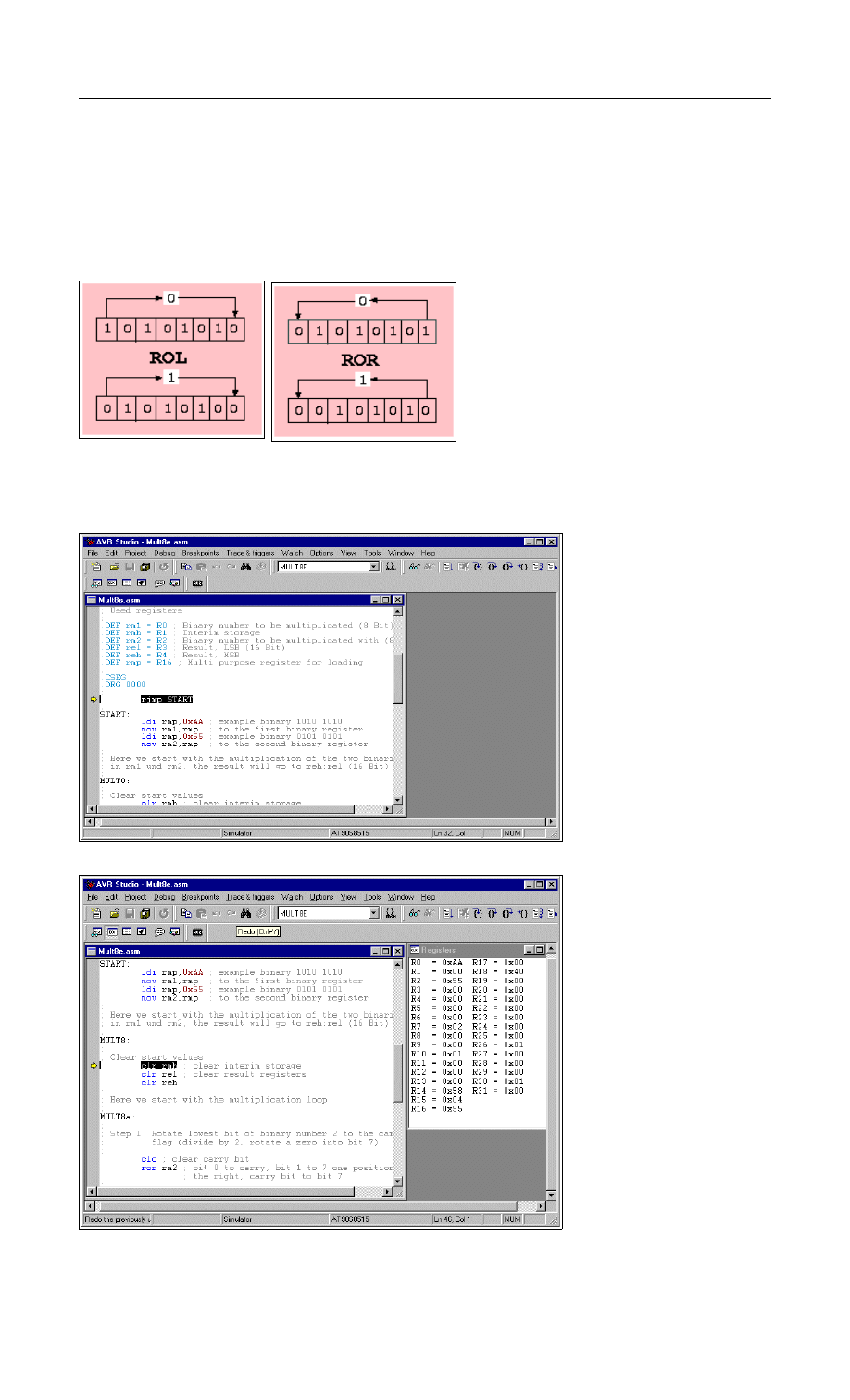
Avr-Asm-Tutorial
32
http://www.avr-asm-tutorial.net
; End of the multiplication, result in reh:rel
;
; Endless loop
;
LOOP:
rjmp loop
Binary rotation
For understanding the multiplication operation,
it is necessary to understand the binary
rotation commands ROL and ROR. These
instructions shift all bits of a register one
position left (ROL) resp. right (ROR). The void
position in the register is filled with the content
of the carry bit of the status register, the bit that
rolls out of the register is shifted to the carry
bit. This operation is demonstrated using 0xAA
as an example for ROL and 0x55 as an
example for ROR.
Multiplication in the studio
The following screenshots show the multiplication program in the simulator.
The object-code has been
opened, the cursor is placed
on the first executable
instruction. F11 does single
steps.
The registers R0 and R2 are
set to 0xAA and 0x55, our test
binaries, to be multiplied.
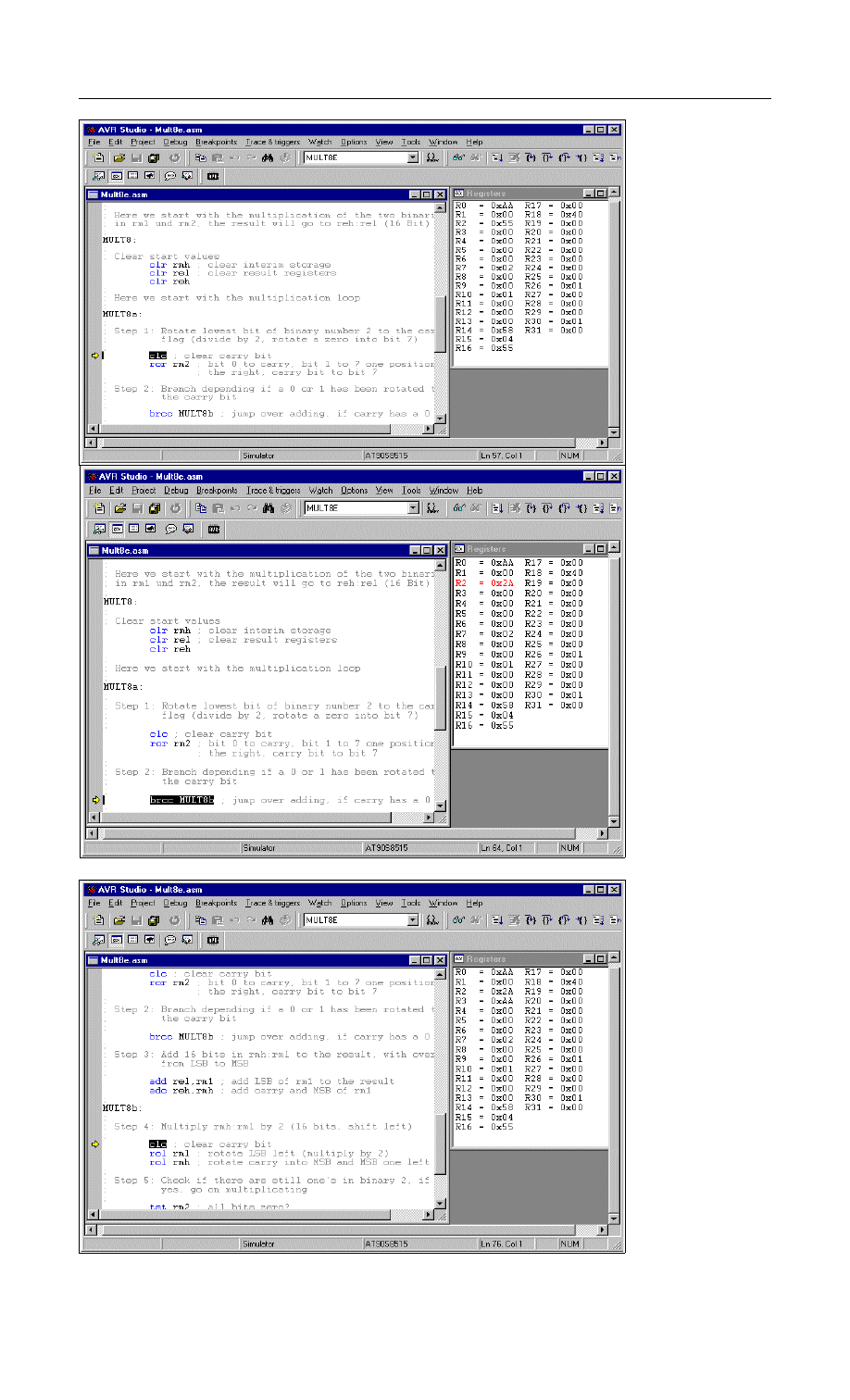
Avr-Asm-Tutorial
33
http://www.avr-asm-tutorial.net
R2 is rotated to the
right, to roll the least
significant bit into the
carry bit. 0x55
(0101.0101) yielded
0x2A (0010.1010).
Because the carry bit
had a one the
content of the
registers R1:R0 is
added to the (empty)
register pair R4:R3,
resulting in 0x00AA
there.
Now the register pair
R1:R0 is rotated one
position left to
multiply this binary
by 2. From 0x00AA,
multiplication by 2
yields 0x0154.
The whole multipli-
cation loop is repea-
ted as long there is
at least one binary 1
in register R2. These
following loops are
not shown here.
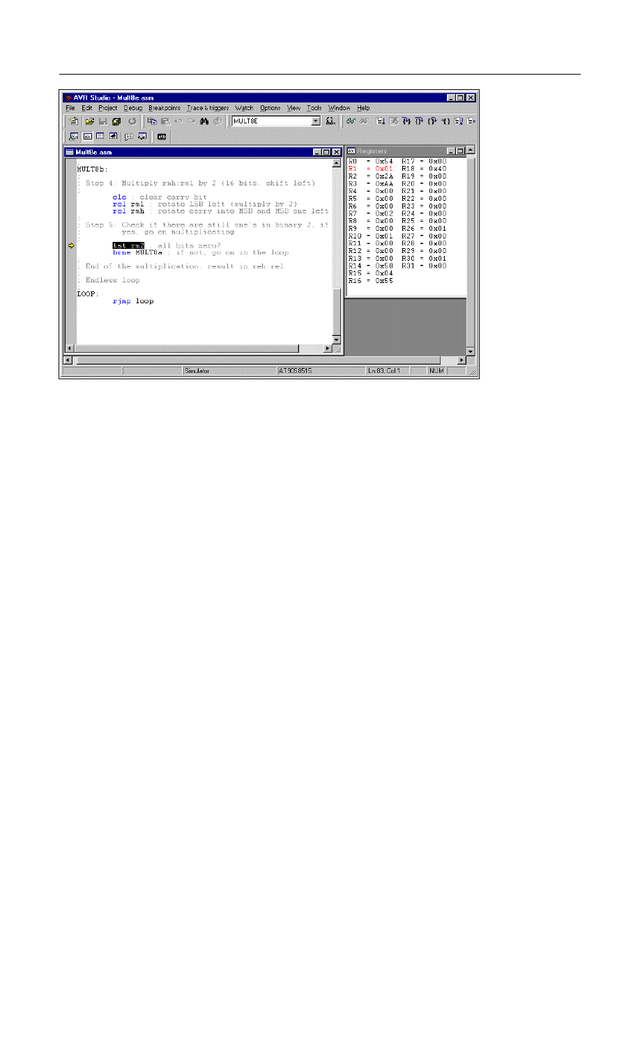
Avr-Asm-Tutorial
34
http://www.avr-asm-tutorial.net
Using key F5 of the
studio we multi-
stepped over these
loops to a break-
point at the end of
the multiplication
routine. The result
register pair R4:R3
has the result of
the multiplication of
0xAA by 0x55:
0x3872.
This wasn't that complicated, just remind yourself on the similiar decimal operations. Binary multiplication
is much easier than decimal.
Division
Decimal division
Again we start with the decimal division, to better understand the binary division. We assume a division of
5678 by 12. This is done like this:
5678 : 12 = ?
--------------------------
- 4 * 1200 = 4800
----
878
- 7 * 120 = 840
---
38
- 3 * 12 = 36
--
2
Result: 5678 : 12 = 473 Remainder 2
===================================
Binary division
In binary the multiplication of the second number (4 * 1200, etc.) is not necessary, due to the fact that we
have only 0 and 1 as digits. Unfortunately binary numbers have much more single digits than their decimal
equivalent, so transferring the decimal division to its binary equivalent is a little bit inconvenient. So the
program works a bit different than that.
The division of a 16-bit binary number by a 8-bit binary in AVR assembler is listed in the following section.
; Div8 divides a 16-bit-number by a 8-bit-number (Test: 16-bit-number: 0xAAAA, 8-bit-number: 0x55)
.NOLIST
.INCLUDE "C:\avrtools\appnotes\8515def.inc"
.LIST
; Registers
.DEF rd1l = R0 ; LSB 16-bit-number to be divided
.DEF rd1h = R1 ; MSB 16-bit-number to be divided
.DEF rd1u = R2 ; interim register
.DEF rd2 = R3 ; 8-bit-number to divide with
.DEF rel = R4 ; LSB result
.DEF reh = R5 ; MSB result
.DEF rmp = R16; multipurpose register for loading
;
.CSEG
.ORG 0
rjmp start
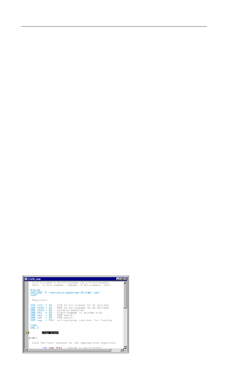
Avr-Asm-Tutorial
35
http://www.avr-asm-tutorial.net
start:
; Load the test numbers to the appropriate registers
ldi rmp,0xAA ; 0xAAAA to be divided
mov rd1h,rmp
mov rd1l,rmp
ldi rmp,0x55 ; 0x55 to be divided with
mov rd2,rmp
; Divide rd1h:rd1l by rd2
div8:
clr rd1u ; clear interim register
clr reh ; clear result (the result registers
clr rel ; are also used to count to 16 for the
inc rel ; division steps, is set to 1 at start)
; Here the division loop starts
div8a:
clc ; clear carry-bit
rol rd1l ; rotate the next-upper bit of the number
rol rd1h ; to the interim register (multiply by 2)
rol rd1u
brcs div8b ; a one has rolled left, so subtract
cp rd1u,rd2 ; Division result 1 or 0?
brcs div8c ; jump over subtraction, if smaller
div8b:
sub rd1u,rd2; subtract number to divide with
sec ; set carry-bit, result is a 1
rjmp div8d ; jump to shift of the result bit
div8c:
clc ; clear carry-bit, resulting bit is a 0
div8d:
rol rel ; rotate carry-bit into result registers
rol reh
brcc div8a ; as long as zero rotate out of the result registers: go on with the division loop
; End of the division reached
stop:
rjmp stop ; endless loop
Program steps during division
During execution of the program the following steps are ran:
•
Definition and preset of the registers with the test binaries,
•
presetting the interim register and the result register pair (the result registers are presetted to
0x0001! After 16 rotations the rolling out of the one stops further division steps.),
•
the 16-bit-binary in rd1h:rd1l is rotated bitwise to the interim register rd1u (multiplication by 2), if a 1
is rotated out of rd1u, the program branches to the subtraction step in step 4 immediately,
•
the content of the interim register is compared with the 8-bit binarly in rd2, if rd2 is smaller it is
subtracted from the interim register and the carry-bit is set to one, if rd2 is greater the subtraction is
skipped and a zero is set to the carry flag,
•
the content of the carry flag is rotated into the result register reh:rel from the right,
•
if a zero rotated out of the result register, we have to repeat the division loop, if it was a one the
division is completed.
If you don't understand rotation yet you'll find this operation discussed in the multiplication section.
Division in the simulator
The following screen shots demonstrate the
program steps in the studio. To do this, you
have to assemble the source code and
open the resulting object file in the studio.
The object code has been started, the
cursor is on the first executable instruction.
The key F11 performs single steps.
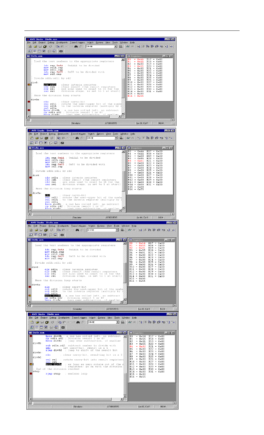
Avr-Asm-Tutorial
36
http://www.avr-asm-tutorial.net
The test binaries 0xAAAA and
0x55, to be divided, are
written to the registers R1:R0
and R3.
The interim register R2 and
the result register pair are set
to their predfined values.
R1:R0 was rotated left to R2,
from 0xAAAA the doubled
value of 0x015554 was
yielded.
No overflow from rotation
into carry has occurred and
0x01 in R2 was smaller than
0x55 in R3, so subtraction
was skipped. A zero in the
carry is rotated into the result
register R5:R4. The former
content of the result register,
a single 1-bit in position 0
has rotated to position 1
(content now: 0x0002). As a
zero was rotated out of the
result register pair, the next
step to be executed is a
branch to the beginning of
the division loop start and
the loop is repeated.
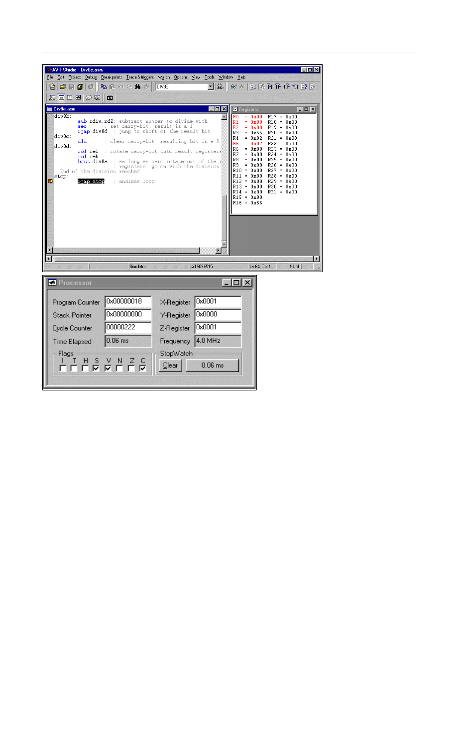
Avr-Asm-Tutorial
37
http://www.avr-asm-tutorial.net
After executing the loop
16 times we have
reached the breakpoint
set at the end of the
division routine. The
result register in R5:R4
holds 0x0202, the result
of the division. The
registers R2:R1:R0 are
empty, so we do not
have a remainder left. If
a remainder would have
been resulted we can
use it to decide whether
an incrementation of the
result should take place,
rounding of the result up.
This step is not coded
here.
The whole division needs 60 micro-seconds
processor time (open a processor view in
the studio menue). A rather long time for a
division.
Number conversion
Number conversion routines are not included here. Please refer to the website, if you need the source
code or a better understanding.
Decimal Fractions
First: Do not use any floating points, unless you really need them. Floating points are resource killers in an
AVR, lame ducks und need extreme execution times. Run into this dilemma, if you think assembler is too
complicated, and you prefer Basic or other languages like C and Pascal.
Not so, if you use assembler. You'll be shown here, how you can perform the multiplication of a fixed point
real number in less than 60 micro-seconds, in special cases even within 18 micro-seconds, at 4 Mcs/s
clock frequency. Without any floating point processor extensions and other expensive tricks for people too
lazy to use their brain.
How to do that? Back to the roots of math! Most tasks with floating point reals can be done using integer
numbers. Integers are easy to program in assembler and perform fast. The decimal point is only in the
brain of the programmer, and is added somewhere in the decimal digit stream. No one realizes, that this is
a trick.
Linear conversions
As an example the following task: an 8-Bit-AD-Converter measures an input signal in the range from 0.00
to 2.55 Volt, and returns as the result a binary in the range from $00 and $FF. The result, a voltage, is to
be displayed on a LCD display. Silly example, as it is so easy: The binary is converted to a decimal ASCII
string between 000 and 255, and just behind the first digit the decimal point has to be inserted. Done!
The electronics world sometimes is more complicated. E.g., the AD-Converter returns an 8-Bit-Hex for
input voltages between 0.00 and 5.00 Volt. Now we're tricked and do not know how to proceed. To display
the correct result on the LCD we would have to multiply the binary by 500/255, which is 1.9608. This is a
silly number, as it is almost 2, but only almost. And we don't want that kind of inaccuracy of 2%, while we
have an AD-converter with around 0.25% accuracy.
To cope with this, we multiply the input by 500/255*256 or 501.96 and divide the result by 256. Why first

Avr-Asm-Tutorial
38
http://www.avr-asm-tutorial.net
multiply by 256 and then divide by 256? It's just for enhanced accuracy. If we multiply the input by 502
instead of 501.96, the error is just in the order of 0.008%. That is good enough for our AD-converter, we
can live with that. And dividing by 256 is an easy task, because it is a well-known power of 2. By dividing
with numbers that are a power of 2, the AVR feels very comfortable and performs very fast. By dividing
with 256, the AVR is even faster, because we just have to skip the last byte of the binary number. Not even
shift and rotate!
The multiplication of an 8-bit-binary with the 9-bit-binary 502 (hex 1F6) can have a result greater than 16
bits. So we have to reserve 24 bits or 3 registers for the result. During multiplication, the constant 502 has
to be shifted left (multiplication by 2) to add these numbers to the result each time a one rolls out of the
input number. As this might need eight shifts left, we need futher three bytes for this constant. So we
chose the following combination of registers for the multiplication:
Number
Value (example)
Register
Input value
255
R1
Multiplicator
502
R4 : R3 : R2
Result
128,010
R7 : R6 : R5
After filling the value 502 (00.01.F6) to R4 : R3 : R2 and clearing the result registers R7 : R6 : R5 the
multiplication goes like this:
1.Test, if the input number is already zero. If yes, we're done.
2.If no, one bit of the input number is shifted out of the register to the right, into the carry, while a zero
is stuffed into bit 7. This instruction is named Logical-Shight-Right or LSR.
3.If the bit in carry is a one, we add the multiplicator (during step 1 the value 502, in step 2 it's 1004,
a.s.o.) to the result. During adding, we care for any carry (adding R2 to R5 by ADD, adding R3 to R6
and R4 to R7 with the ADC instruction!). If the bit in the carry was a zero, we just don't add the
multiplicator to the result and jump to the next step.
4.Now the multiplicator is multiplied by 2, because the next bit shifted out of the input number is worth
double as much. So we shift R2 to the left (by inserting a zero in bit 0) using LSL. Bit 7 is shifted to
the carry. Then we rotate this carry into R3, rotating its content left one bit, and bit 7 to the carry. The
same with R4.
5.Now we're done with one digit of the input number, and we proceed with step 1 again.
The result of the multiplication by 502 now is in the result registers R7 : R6 : R5. If we just ignore register
R5 (division by 256), we have our desired result. To enhance occuracy, we can use bit 7 in R5 to round
the result. Now we just have to convert the result from its binary form to decimal ASCII (see Conversion
bin to decimal-ASCII on the website). If we just add a decimal point in the right place in the ASCII string,
our voltage string is ready for the display.
The whole program, from the input number to the resulting ASCII string, requires between 79 and 228
clock cycles, depending from the input number. Those who want to beat this with the floating point routine
of a more sophisticated language than assembler, feel free to mail me your conversion time (and program
flash and memory usage).
Example 1: 8bitADconverter with fixed decimal output
; Demonstrates floating point conversion in Assembler, (C)2003 www.avr-asm-tutorial.net
;
; The task: You read in an 8-bit result of an analogue-digital-converter, number is in the range from hex 00 to FF.
; You need to convert this into a floating point number in the range from 0.00 to 5.00 Volt
; The program scheme:
; 1. Multiplication by 502 (hex 01F6).That step multiplies by 500, 256 and divides by 255 in one step!
; 2. Round the result and cut the last byte of the result. This step divides by 256 by ignoring the last byte of the result.
; Before doing that, bit 7 is used to round the result.
; 3. Convert the resulting word to ASCII and set the correct decimal sign. The resulting word in the range from 0 to 500
; is displayed in ASCII-characters as 0.00 to 5.00.
; The registers used:
; The routines use the registers R8..R1 without saving these before. Also required is a multipurpose register called rmp,
; located in the upper half of the registers. Please take care that these registers don't conflict with the register use in the
; rest of your program.
; When entering the routine the 8-bit number is expected in the register R1. The multiplication uses R4:R3:R2 to hold
; the multiplicator 502 (is shifted left max. eight times during multiplication). The result of the multiplication is calculated
; in the registers R7:R6:R5. The result of the so called division by 256 by just ignoring R5 in the result, is in R7:R6. R7:R6
; is rounded, depending on the highest bit of R5, and the result is copied to R2:R1.
; Conversion to an ASCII-string uses the input in R2:R1, the register pair R4:R3 as a divisor for conversion, and places the
; ASCII result string to R5:R6:R7:R8 (R6 is the decimal char).
; Other conventions:
; The conversion uses subroutines and the stack.The stack must work fine for the use of three levels (six bytes SRAM).

Avr-Asm-Tutorial
39
http://www.avr-asm-tutorial.net
; Conversion times:
; The whole routine requires 228 clock cycles maximum (converting $FF), and 79 clock cycles minimum (converting $00).
; At 4 MHz the times are 56.75 microseconds resp. 17.75 microseconds.
; Definitions:
; Registers
.DEF rmp = R16 ; used as multi-purpose register
; AVR type: Tested for type AT90S8515, only required for stack setting, routines work fine with other AT90S-types also
.NOLIST
.INCLUDE "8515def.inc"
.LIST
; Start of test program
; Just writes a number to R1 and starts the conversion routine, for test purposes only
.CSEG
.ORG $0000
rjmp main
main:
ldi rmp,HIGH(RAMEND) ; Set the stack
out SPH,rmp
ldi rmp,LOW(RAMEND)
out SPL,rmp
ldi rmp,$FF ; Convert $FF
mov R1,rmp
rcall fpconv8 ; call the conversion routine
no_end: ; unlimited loop, when done
rjmp no_end
; Conversion routine wrapper, calls the different conversion steps
fpconv8:
rcall fpconv8m ; multiplicate by 502
rcall fpconv8r ; round and divide by 256
rcall fpconv8a ; convert to ASCII string
ldi rmp,'.' ; set decimal char
mov R6,rmp
ret ; all done
; Subroutine multiplication by 502
fpconv8m:
clr R4 ; set the multiplicant to 502
ldi rmp,$01
mov R3,rmp
ldi rmp,$F6
mov R2,rmp
clr R7 ; clear the result
clr R6
clr R5
fpconv8m1:
or R1,R1 ; check if the number is all zeros
brne fpconv8m2 ; still one's, go on convert
ret ; ready, return back
fpconv8m2:
lsr R1 ; shift number to the right (div by 2)
brcc fpconv8m3 ; if the lowest bit was 0, then skip adding
add R5,R2 ; add the number in R6:R5:R4:R3 to the result
adc R6,R3
adc R7,R4
fpconv8m3:
lsl R2 ; multiply R4:R3:R2 by 2
rol R3
rol R4
rjmp fpconv8m1 ; repeat for next bit
; Round the value in R7:R6 with the value in bit 7 of R5
fpconv8r:
clr rmp ; put zero to rmp
lsl R5 ; rotate bit 7 to carry
adc R6,rmp ; add LSB with carry
adc R7,rmp ; add MSB with carry
mov R2,R7 ; copy the value to R2:R1 (divide by 256)
mov R1,R6
ret
; Convert the word in R2:R1 to an ASCII string in R5:R6:R7:R8
fpconv8a:
clr R4 ; Set the decimal divider value to 100
ldi rmp,100
mov R3,rmp
rcall fpconv8d ; get ASCII digit by repeated subtraction
mov R5,rmp ; set hundreds string char
ldi rmp,10 ; Set the decimal divider value to 10
mov R3,rmp
rcall fpconv8d ; get the next ASCII digit
mov R7,rmp ; set tens string char
ldi rmp,'0' ; convert the rest to an ASCII char
add rmp,R1
mov R8,rmp ; set ones string char
ret

Avr-Asm-Tutorial
40
http://www.avr-asm-tutorial.net
; Convert binary word in R2:R1 to a decimal digit by substracting the decimal divider value in R4:R3 (100, 10)
fpconv8d:
ldi rmp,'0' ; start with decimal value 0
fpconv8d1:
cp R1,R3 ; Compare word with decimal divider value
cpc R2,R4
brcc fpconv8d2 ; Carry clear, subtract divider value
ret ; done subtraction
fpconv8d2:
sub R1,R3 ; subtract divider value
sbc R2,R4
inc rmp ; up one digit
rjmp fpconv8d1 ; once again
; End of conversion test routine
Example 2: 10bitADconverter with fixed decimal output
This example is a bit more complicated. Refer to the website if you need it.
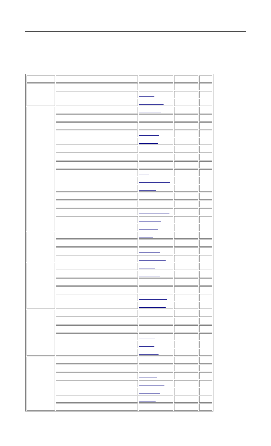
Avr-Asm-Tutorial
41
http://www.avr-asm-tutorial.net
Annex
Commands sorted by function
For the abbreviations used see the list of abbreviations.
Function
Subfunction
Command
Flags
Clk
Register
set
0
CLR r1
Z N V
1
255
SER rh
1
Constant
LDI rh,c255
1
Copy
Register => Register
MOV r1,r2
1
SRAM => Register, direct
LDS r1,c65535
2
SRAM => Register
LD r1,rp
2
SRAM => Register and INC
LD r1,rp+
2
DEC, SRAM => Register
LD r1,-rp
2
SRAM, displaced => Register
LDD r1,ry+k63
2
Port => Register
IN r1,p1
1
Stack => Register
POP r1
2
Program storage Z => R0
LPM
3
Register => SRAM, direct
STS c65535,r1
2
Register => SRAM
ST rp,r1
2
Register => SRAM and INC
ST rp+,r1
2
DEC, Register => SRAM
ST -rp,r1
2
Register => SRAM, displaced
STD ry+k63,r1
2
Register => Port
OUT p1,r1
1
Register => Stack
PUSH r1
2
Add
8 Bit, +1
INC r1
Z N V
1
8 Bit
ADD r1,r2
Z C N V H 1
8 Bit + Carry
ADC r1,r2
Z C N V H 1
16 Bit, constant
ADIW rd,k63
Z C N V S 2
Subtract
8 Bit, -1
DEC r1
Z N V
1
8 Bit
SUB r1,r2
Z C N V H 1
8 Bit, constant
SUBI rh,c255
Z C N V H 1
8 Bit - Carry
SBC r1,r2
Z C N V H 1
8 Bit - Carry, constant
SBCI rh,c255
Z C N V H 1
16 Bit
SBIW rd,k63
Z C N V S 2
Shift
logic, left
LSL r1
Z C N V
1
logic, right
LSR r1
Z C N V
1
Rotate, left over Carry
ROL r1
Z C N V
1
Rotate, right over Carry
ROR r1
Z C N V
1
Arithmetic, right
ASR r1
Z C N V
1
Nibble exchange
SWAP r1
1
Binary
And
AND r1,r2
Z N V
1
And, constant
ANDI rh,c255
Z N V
1
Or
OR r1,r2
Z N V
1
Or, constant
ORI rh,c255
Z N V
1
Exclusive-Or
EOR r1,r2
Z N V
1
Ones-complement
COM r1
Z C N V
1
Twos-complement
NEG r1
Z C N V H 1
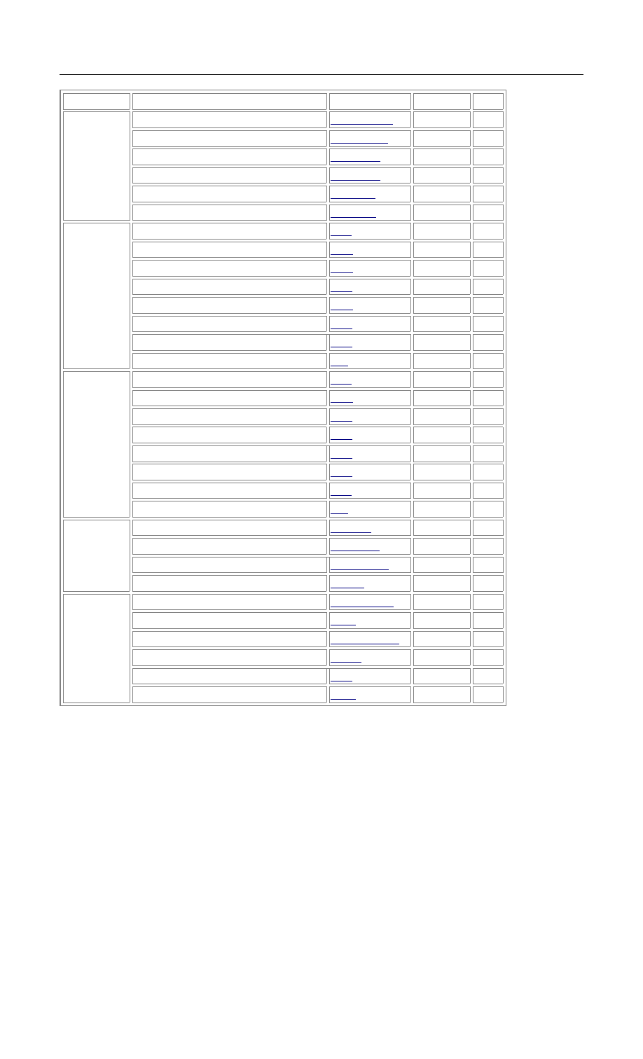
Avr-Asm-Tutorial
42
http://www.avr-asm-tutorial.net
Function
Subfunction
Command
Flags
Clk
Bits
change
Register, set
SBR rh,c255
Z N V
1
Register, clear
CBR rh,255
Z N V
1
Register, copy to T-Flag
BST r1,b7
T
1
Register, copy from T-Flag
BLD r1,b7
1
Port, set
SBI pl,b7
2
Port, clear
CBI pl,b7
2
Statusbit
set
Zero-Flag
SEZ
Z
1
Carry Flag
SEC
C
1
Negative Flag
SEN
N
1
Twos complement carry Flag
SEV
V
1
Half carry Flag
SEH
H
1
Signed Flag
SES
S
1
Transfer Flag
SET
T
1
Interrupt Enable Flag
SEI
I
1
Statusbit
clear
Zero-Flag
CLZ
Z
1
Carry Flag
CLC
C
1
Negative Flag
CLN
N
1
Twos complement carry Flag
CLV
V
1
Half carry Flag
CLH
H
1
Signed Flag
CLS
S
1
Transfer Flag
CLT
T
1
Interrupt Enable Flag
CLI
I
1
Compare
Register, Register
CP r1,r2
Z C N V H 1
Register, Register + Carry
CPC r1,r2
Z C N V H 1
Register, constant
CPI rh,c255
Z C N V H 1
Register, 0
≤
TST r1
Z N V
1
Immediate
Jump
Relative
RJMP c4096
2
Indirect, Address in Z
IJMP
2
Subroutine, relative
RCALL c4096
3
Subroutine, Address in Z
ICALL
3
Return from Subroutine
RET
4
Return from Interrupt
RETI
I
4
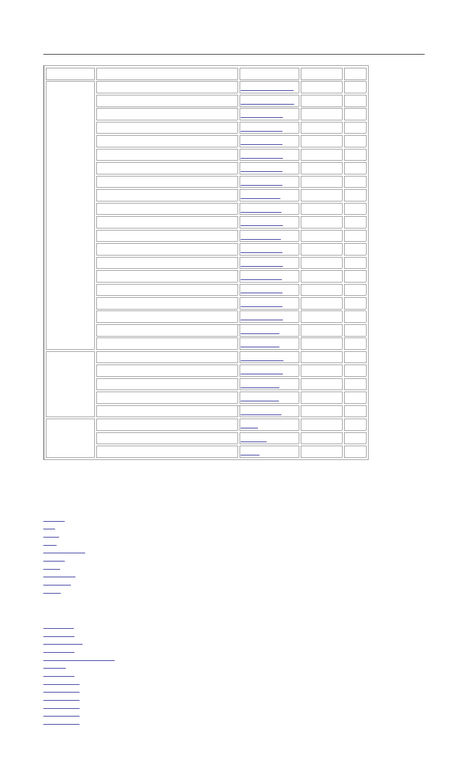
Avr-Asm-Tutorial
43
http://www.avr-asm-tutorial.net
Function
Subfunction
Command
Flags
Clk
Conditioned
Jump
Statusbit set
BRBS b7,c127
1/2
Statusbit clear
BRBC b7,c127
1/2
Jump if equal
BREQ c127
1/2
Jump if equal
BRNE c127
1/2
Jump if carry
BRCS c127
1/2
Jump if carry clear
BRCC c127
1/2
Jump if equal or greater
BRSH c127
1/2
Jump if lower
BRLO c127
1/2
Jump if negative
BRMI c127
1/2
Jump if positive
BRPL c127
1/2
Jump if greater or equal (Signed)
BRGE c127
1/2
Jump if lower than zero (Signed)
BRLT c127
1/2
Jump on half carry set
BRHS c127
1/2
Jump if half carry clear
BRHC c127
1/2
Jump if T-Flag set
BRTS c127
1/2
Jump if T-Flag clear
BRTC c127
1/2
Jump if Twos complement carry set
BRVS c127
1/2
Jump if Twos complement carry clear
BRVC c127
1/2
Jump if Interrupts enabled
BRIE c127
1/2
Jump if Interrupts disabled
BRID c127
1/2
Conditioned
Jumps
Registerbit=0
SBRC r1,b7
1/2/3
Registerbit=1
SBRS r1,b7
1/2/3
Portbit=0
SBIC pl,b7
1/2/3
Portbit=1
SBIS pl,b7
1/2/3
Compare, jump if equal
CPSE r1,r2
1/2/3
Others
No Operation
NOP
1
Sleep
SLEEP
1
Watchdog Reset
WDR
1
Command list in alphabetic order
Assembler directives
.CSEG
.DB
.DEF
.DW
.ENDMACRO
.ESEG
.EQU
.INCLUDE
.MACRO
.ORG
Commands
ADC r1,r2
ADD r1,r2
ADIW rd,k63
AND r1,r2
ANDI rh,c255, Register
ASR r1
BLD r1,b7
BRCC c127
BRCS c127
BREQ c127
BRGE c127
BRHC c127
BRHS c127

Avr-Asm-Tutorial
44
http://www.avr-asm-tutorial.net
BRID c127
BRIE c127
BRLO c127
BRLT c127
BRMI c127
BRNE c127
BRPL c127
BRSH c127
BRTC c127
BRTS c127
BRVC c127
BRVS c127
BST r1,b7
CBI pl,b7
CBR rh,255, Register
CLC
CLH
CLI
CLN
CLR r1
CLS
CLT, (command example)
CLV
CLZ
COM r1
CP r1,r2
CPC r1,r2
CPI rh,c255, Register
CPSE r1,r2
DEC r1
EOR r1,r2
ICALL
IJMP IN r1,p1
INC r1
LD rp,(rp,rp+,-rp) (Register), (SRAM access), Ports
LDD r1,ry+k63
LDI rh,c255 (Register), Pointer
LDS r1,c65535
LPM
LSL r1
LSR r1
MOV r1,r2
NEG r1
NOP
OR r1,r2 ORI rh,c255 OUT p1,r1
POP r1, (in Int-routine)
PUSH r1, (in Int-routine)
RCALL c4096
RET, (in Int-routine)
RETI
RJMP c4096
ROL r1
ROR r1
SBC r1,r2
SBCI rh,c255
SBI pl,b7
SBIC pl,b7
SBIS pl,b7
SBIW rd,k63
SBR rh,255, Register
SBRC r1,b7
SBRS r1,b7
SEC
SEH
SEI, (in Int-routine)
SEN
SER rh
SES
SET, (example)
SEV
SEZ
SLEEP
ST (rp/rp+/-rp),r1 (Register), SRAM access, Ports
STD ry+k63,r1
STS c65535,r1
SUB r1,r2
SUBI rh,c255
SWAP r1
TST r1
WDR
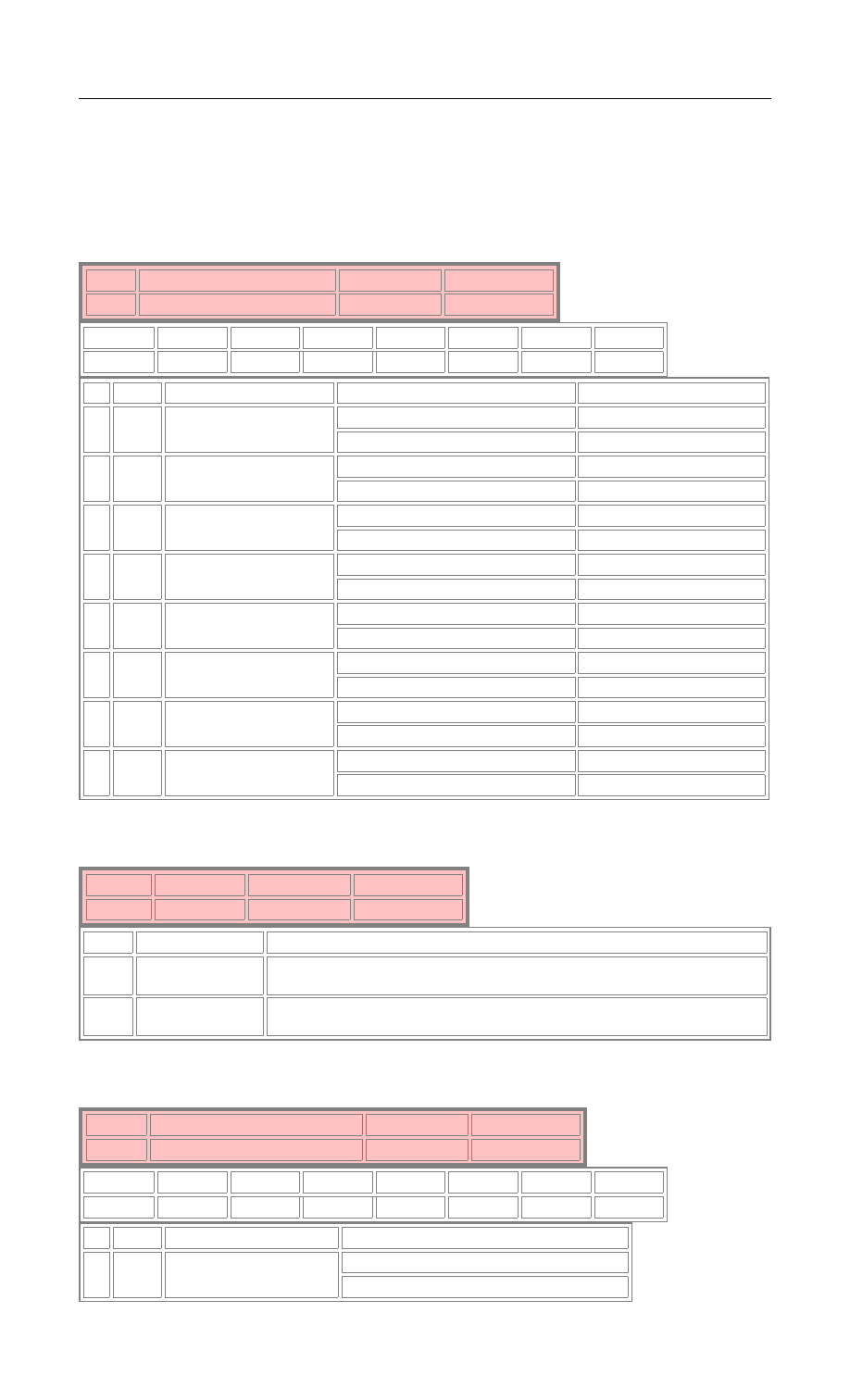
Avr-Asm-Tutorial
45
http://www.avr-asm-tutorial.net
Port details
The table of the relevant ports in the ATMEL AVR types AT90S2313, 2323 and 8515. Bytewise
accessable ports or register pairs are not displayed in detail. No warranty for correctness, see the original
data sheets!
StatusRegister, Accumulator flags
Port
Function
Port-Address RAM-Address
SREG Status Register Accumulator 0x3F
0x5F
7
6
5
4
3
2
1
0
I
T
H
S
V
N
Z
C
Bit Name
Meaning
Opportunities
Conmmand
7
I
Global Interrupt Flag
0: Interrupts disabled
CLI
1: Interrupts enabled
SEI
6
T
Bit storage
0: Stored bit is 0
CLT
1: Stored bit is 1
SET
5
H
Halfcarry-Flag
0: No halfcarry occured
CLH
1: Halfcarry occured
SEH
4
S
Sign-Flag
0: Sign positive
CLS
1: Sign negative
SES
3
V
Two's complement-Flag
0: No carry occured
CLV
1: Carry occured
SEV
2
N
Negative-Flag
0: Result was not negative/smaller
CLN
1: Result was negative/smaller
SEN
1
Z
Zero-Flag
0: Result was not zero/unequal
CLZ
1: Result was zero/equal
SEZ
0
C
Carry-Flag
0: No carry occured
CLC
1: Carry occured
SEC
Stackpointer
Port
Function
Port-Address RAM-Address
SPL/SPH Stackpointer 003D/0x3E
0x5D/0x5E
Name
Meaning
Availability
SPL
Low-Byte of
Stackpointer
From AT90S2313 upwards, not in 1200
SPH
High-Byte of
Stackpointer
From AT90S8515 upwards, only in devices with >256 bytes internal SRAM
SRAM and External Interrupt control
Port
Function
Port-Address RAM-Address
MCUCR MCU General Control Register 0x35
0x55
7
6
5
4
3
2
1
0
SRE
SRW
SE
SM
ISC11
ISC10
ISC01
ISC00
Bit Name
Meaning
Opportunities
7
SRE
Ext.SRAM Enable
0=No external SRAM connected
1=External SRAM connected
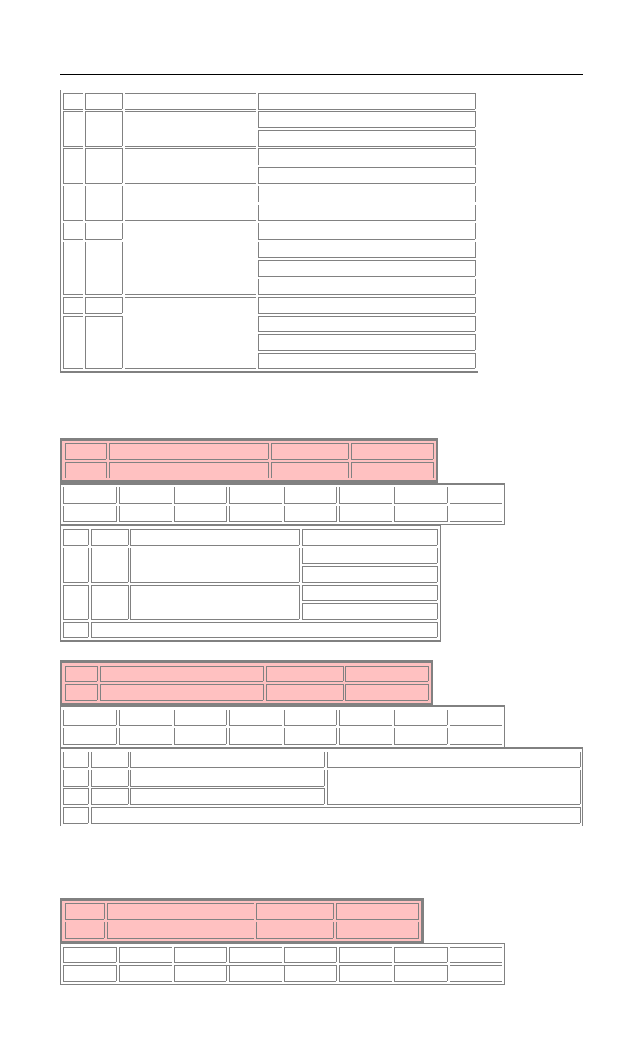
Avr-Asm-Tutorial
46
http://www.avr-asm-tutorial.net
Bit Name
Meaning
Opportunities
6
SRW
Ext.SRAM Wait States
0=No extra wait state on external SRAM
1=Additional wait state on external SRAM
5
SE
Sleep Enable
0=Ignore SLEEP commands
1=SLEEP on command
4
SM
Sleep Mode
0=Idle Mode (Half sleep)
1=Power Down Mode (Full sleep)
3
ISC11
2
ISC10
Interrupt control Pin INT1
(connected to GIMSK)
00: Low-level initiates Interrupt
01: Undefined
10: Falling edge triggers interrupt
11: Rising edge triggers interrupt
1
ISC01
0
ISC00
Interrupt control Pin INT0
(connected to GIMSK)
00: Low-level initiates interrupt
01: Undefined
10: Falling edge triggers interrupt
11: Rising edge triggers interrupt
External Interrupt Control
Port
Function
Port-Address RAM-Address
GIMSK General Interrupt Maskregister 0x3B
0x5B
7
6
5
4
3
2
1
0
INT1
INT0
-
-
-
-
-
-
Bit Name
Meaning
Opportunities
7
INT1
Interrupt by external pin INT1
(connected to mode in MCUCR)
0: External INT1 disabled
1: External INT1 enabled
6
INT0
Interrupt by external Pin INT0
(connected to mode in MCUCR)
0: External INT0 disabled
1: External INT0 enabled
0...5
(Not used)
Port
Function
Port-Address RAM-Address
GIFR General Interrupt Flag Register 0x3A
0x5A
7
6
5
4
3
2
1
0
INTF1
INTF0
-
-
-
-
-
-
Bit Name
Meaning
Opportunities
7
INTF1 Interrupt by external pin INT1 occured
6
INTF0 Interrupt by external pin INT0 occured
Automatic clear by execution of the Int-Routine or
Clear by command
0...5
(Not used)
Timer Interrupt Control
Port
Function
Port-Address RAM-Address
TIMSK Timer Interrupt Maskregister 0x39
0x59
7
6
5
4
3
2
1
0
TOIE1
OCIE1A
OCIE1B
-
TICIE1
-
TOIE0
-
Avr-Asm-Tutorial
47
http://www.avr-asm-tutorial.net
Bit
Name
Meaning
Opportunities
7
TOIE1
Timer/Counter 1 Overflow-Interrupt
0: No Int at overflow
1: Int at overflow
6
OCIE1A Timer/Counter 1 Compare A Interrupt
0: No Int at equal A
1: Int at equal A
5
OCIE1B Timer/Counter 1 Compare B Interrupt
0: No Int at B
1: Int at equal B
4
(Not used)
3
TICIE1
Timer/Counter 1 Capture Interrupt
0: No Int at Capture
1: Int at Capture
2
(Not used)
1
TOIE0
Timer/Counter 0 Overflow-Interrupt
0: No Int at overflow
1: Int at overflow
0
(Not used)
Port
Function
Port-Address RAM-Address
TIFR Timer Interrupt Flag Register 0x38
0x58
7
6
5
4
3
2
1
0
TOV1
OCF1A
OCF1B
-
ICF1
-
TOV0
-
Bit Name
Meaning
Opportunities
7
TOV1
Timer/Counter 1 Overflow reached
6
OCF1A Timer/Counter 1 Compare A reached
5
OCF1B Timer/Counter 1 Compare B reached
4
(Not used)
3
ICF1
Timer/Counter 1 Capture-Event occured
2
(not used)
1
TOV0
Timer/Counter 0 Overflow occured
0
(not used)
Interrupt-Mode:
Automatic Clear
by execution of the
Int-Routine
OR
Polling-Mode:
Clear by
command
Timer/Counter 0
Port
Function
Port-Address RAM-Address
TCCR0 Timer/Counter 0 Control Register
0x33
0x53
7
6
5
4
3
2
1
0
-
-
-
-
-
CS02
CS01
CS00
Bit
Name
Meaning
Opportunities
2..0 CS02..CS00 Timer Clock
000: Stop Timer
001: Clock = Chip clock
010: Clock = Chip clock / 8
011: Clock = Chip clock / 64
100: Clock = Chip clock / 256
101: Clock = Chip clock / 1024
110: Clock = falling edge of external Pin T0
111: Clock = rising edge of external Pin T0
3..7
(not used)
Avr-Asm-Tutorial
48
http://www.avr-asm-tutorial.net
Port
Function
Port-Address RAM-Address
TCNT0 Timer/Counter 0 count register 0x32
0x52
Timer/Counter 1
Port
Function
Port-Address RAM-Address
TCCR1A Timer/Counter 1 Control Register A
0x2F
0x4F
7
6
5
4
3
2
1
0
COM1A1 COM1A0 COM1B1 COM1B0
-
-
PWM11
PWM10
Bit
Name
Meaning
Opportunities
7
COM1A1
6
COM1A0
Compare Output A
5
COM1B1
4
COM1B0
Compare Output B
00: OC1A/B not connected
01: OC1A/B changes polarity
10: OC1A/B to zero
11: OC1A/B to one
3
2
(not used)
1..0
PWM11
PWM10
Pulse width modulator
00: PWM off
01: 8-Bit PWM
10: 9-Bit PWM
11: 10-Bit PWM
Port
Function
Port-Address RAM-Address
TCCR1B Timer/Counter 1 Control Register B
0x2E
0x4E
7
6
5
4
3
2
1
0
ICNC1
ICES1
-
-
CTC1
CS12
CS11
CS10
Bit
Name
Meaning
Opportunities
7
ICNC1
Noise Canceler
on ICP-Pin
0: disabled, first edge starts sampling
1: enabled, min four clock cycles
6
ICES1
Edge selection
on Capture
0: falling edge triggers Capture
1: rising edge triggers Capture
5..4 (not used)
3
CTC1
Clear at
Compare Match A
1: Counter set to zero if equal
2..0 CS12..CS10 Clock select
000: Counter stopped
001: Clock
010: Clock / 8
011: Clock / 64
100: Clock / 256
101: Clock / 1024
110: falling edge external Pin T1
111: rising edge external Pin T1
Port
Function
Port-Address RAM-Address
TCNT1L/H Timer/Counter 1 count register 0x2C/0x2D
0x4C/0x4D
Avr-Asm-Tutorial
49
http://www.avr-asm-tutorial.net
Port
Function
Port-Address RAM-Address
OCR1AL/H Timer/Counter 1 Output Compare register A
0x2A/0x2B
0x4A/0x4B hex
Port
Function
Port-Address RAM-Address
OCR1BL/H Timer/Counter 1 Output Compare register B
0x28/0x29
0x48/0x49
Port
Function
Port-Address RAM-Address
ICR1L/H Timer/Counter 1 Input Capture Register
0x24/0x25
0x44/0x45
WatchdogTimer
Port
Function
Port-Address RAM-Address
WDTCR Watchdog Timer Control Register
0x21
0x41
7
6
5
4
3
2
1
0
-
-
-
WDTOE
WDE
WDP2
WDP1
WDP0
Bit
Name
Meaning
WDT-cycle at 5.0 Volt
7..5
(not used)
4
WDTOE
Watchdog Turnoff Enable
Previous set to
disabling of WDE required
3
WDE
Watchdog Enable
1: Watchdog aktive
2..0 WDP2..WDP0 Watchdog Timer Prescaler
000: 15 ms
001: 30 ms
010: 60 ms
011: 120 ms
100: 240 ms
101: 490 ms
110: 970 ms
111: 1,9 s
EEPROM
Port
Function
Port-Address RAM-Address
EEARL/H EEPROM Address Register
0x1E/0x1F
0x3E/0x3F
EEARH only in types with more than 256 Bytes EEPROM (from AT90S8515 upwards)
Port
Function
Port-Address RAM-Address
EEDR EEPROM Data Register 0x1D
0x3D
Port
Function
Port-Address RAM-Address
EECR EEPROM Control Register
0x1C
0x3C
7
6
5
4
3
2
1
0
-
-
-
-
-
EEMWE
EEWE
EERE
Avr-Asm-Tutorial
50
http://www.avr-asm-tutorial.net
Bit
Name
Meaning
Function
7..
3
(not used)
2
EEMWE EEPROM Master Write Enable
Previous set enables write cycle
1
EEWE
EEPROM Write Enable
Set to initiate write
0
EERE
EEPROM Read Enable
Set initiates read
Serial Peripheral Interface SPI
Port
Function
Port-Address RAM-Address
SPCR SPI Control Register 0x0D
0x2D
7
6
5
4
3
2
1
0
SPIE
SPE
DORD
MSTR
CPOL
CPHA
SPR1
SPR0
Bit Name
Meaning
Function
7
SPIE
SPI Interrupt Enable
0: Interrupts disabled
1: Interrupts enabled
6
SPE
SPI Enable
0: SPI disabled
1: SPI enabled
5
DORD Data Order
0: MSB first
1: LSB first
4
MSTR Master/Slave Select
0: Slave
1: Master
3
CPOL Clock Polarity
0: Positive Clock Phase
1: Negative Clock Phase
2
CPHA Clock Phase
0: Sampling at beginning of Clock Phase
1: Sampling at end of Clock Phase
1
SPR1
0
SPR0
SCK clock frequency
00: Clock / 4
01: Clock / 16
10: Clock / 64
11: Clock / 128
Port
Function
Port-Address RAM-Address
SPSR SPI Status Register 0x0E
0x2E
7
6
5
4
3
2
1
0
SPIF
WCOL
-
-
-
-
-
-
Bit Name
Meaning
Function
7
SPIF
SPI Interrupt Flag
Interrupt request
6
WCOL Write Collision Flag Write collission occured
5..0
(not used)
Port
Function
Port-Address RAM-Address
SPDR SPI Data Register 0x0F
0x2F
Avr-Asm-Tutorial
51
http://www.avr-asm-tutorial.net
UART
Port
Function
Port-Address RAM-Address
UDR UART I/O Data Register 0x0C
0x2C
Port
Function
Port-Address RAM-Address
USR UART Status Register 0x0B
0x2B
7
6
5
4
3
2
1
0
RXC
TXC
UDRE
FE
OR
-
-
-
Bit Name
Meaning
Function
7
RXC
UART Receive Complete
1: Char received
6
TXC
UART Transmit Complete
1: Shift register empty
5
UDRE UART Data Register Empty
1: Transmit register available
4
FE
Framing Error
1: Illegal Stop-Bit
3
OR
Overrun
1: Lost char
2..0
(not used)
Port
Function
Port-Address RAM-Address
UCR UART Control Register 0x0A
0x2A
7
6
5
4
3
2
1
0
RXCIE
TXCIE
UDRIE
RXEN
TXEN
CHR9
RXB8
TXB8
Bit Name
Meaning
Function
7
RXCIE RX Complete Interrupt Enable
1: Interrupt on received char
6
TXCIE TX Complete Interrupt Enable
1: Interrupt at transmit complete
5
UDRIE Data Register Empty Interrupt Enable
1: Interrupt on transmit buffer empty
4
RXEN Receiver Enabled
1: Receiver enabled
3
TXEN
Transmitter Enable
1: Transmitter enabled
2
CHR9
9-bit Characters
1: Char length 9 Bit
1
RXB8
Receive Data Bit 8
9th Data bit on receive
0
TXB8
Transmit Data Bit 8
9.Data bit on transmit
Port
Function
Port-Address RAM-Address
UBRR UART Baud Rate Register 0x09
0x29
Analog Comparator
Port
Function
Port-Address RAM-Address
ACSR Analog Comparator Control and Status Register
0x08
0x28
7
6
5
4
3
2
1
0
ACD
-
ACO
ACI
ACIE
ACIC
ACIS1
ACIS0
Bit Name
Meaning
Function
7
ACD
Disable
Disable Comparators
6
(not used)
5
ACO
Comparator Output
Read: Output of the Comparators
4
ACI
Interrupt Flag
1: Interrupt request
Avr-Asm-Tutorial
52
http://www.avr-asm-tutorial.net
Bit Name
Meaning
Function
3
ACIE
Interrupt Enable
1: Interrupts enabled
2
ACIC
Input Capture Enable 1: Connect to Timer 1 Capture
1
ACIS1
0
ACIS0
Input Capture Enable
00: Interrupt on edge change
01: not used)
10: Interrupt on falling edge
11: Interrupt on rising edge
I/O Ports
Port Register
Function
Port-Address RAM-Address
A
PORTA
Data Register
0x1B
0x3B
DDRA
Data Direction Register
0x1A
0x3A
PINA
Input Pins Address
0x19
0x39
B
PORTB
Data Register
0x18
0x38
DDRB
Data Direction Register
0x17
0x37
PINB
Input Pins Address
0x16
0x36
C
PORTC
Data Register
0x15
0x35
DDRC
Data Direction Register
0x14
0x34
PINC
Input Pins Address
0x13
0x33
D
PORTD
Data Register
0x12
0x32
DDRD
Data Direction Register
0x11
0x31
PIND
Input Pins Address
0x10
0x30
Ports, alphabetic order
ACSR, Analog Comparator Control and Status Register
DDRx, Port x Data Direction Register
EEAR, EEPROM Adress Register
EECR, EEPROM Control Register
EEDR, EEPROM Data Register
GIFR, General Interrupt Flag Register
GIMSK, General Interrupt Mask Register
ICR1L/H, Input Capture Register 1
MCUCR, MCU General Control Register
OCR1A, Output Compare Register 1 A
OCR1B, Output Compare Register 1 B
PINx, Port Input Access
PORTx, Port x Output Register
SPL/SPH, Stackpointer
SPCR, Serial Peripheral Control Register
SPDR, Serial Peripheral Data Register
SPSR, Serial Peripheral Status Register
SREG, Status Register
TCCR0, Timer/Counter Control Register, Timer 0
TCCR1A, Timer/Counter Control Register 1 A
TCCR1B, Timer/Counter Control Register 1 B
TCNT0, Timer/Counter Register, Counter 0
TCNT1, Timer/Counter Register, Counter 1
TIFR, Timer Interrupt Flag Register
TIMSK, Timer Interrupt Mask Register
UBRR, UART Baud Rate Register
UCR, UART Control Register
UDR, UART Data Register
WDTCR, Watchdog Timer Control Register

Avr-Asm-Tutorial
53
http://www.avr-asm-tutorial.net
List of abbreviations
The abbreviations used are chosen to include the value range. Register pairs are named by the lower of
the two registers. Constants in jump commands are automatically calculated from the respective labels
during assembly.
Category Abbrev.
Means ...
Value range
Register
r1
Ordinary Source and Target register
r2
Ordinary Source register
R0..R31
rh
Upper page register
R16..R31
rd
Twin register
R24(R25), R26(R27), R28(R29), R30(R31)
rp
Pointer register
X=R26(R27), Y=R28(R29), Z=R30(R31)
ry
Pointer register with displacement
Y=R28(R29), Z=R30(R31)
Constant
k63
Pointer-constant
0..63
c127
Conditioned jump distance
-64..+63
c255
8-Bit-Constant
0..255
c4096
Relative jump distance
-2048..+2047
c65535
16-Bit-Address
0..65535
Bit
b7
Bit position
0..7
Port
p1
Ordinary Port
0..63
pl
Lower page port
0..31
Wyszukiwarka
Podobne podstrony:
An Introduction to the Kabalah
Introduction to the MOSFET and MOSFET Inverter(1)
Zinda; Introduction to the philosophy of science
IT 0550 US Army Introduction to the Intelligence Analyst
Introduction to the Direct3D 11 Graphics Pipeline
Introduction to the Magnetic Treatment of Fuel
Introduction to the Humanistic Approach
An introduction to the Analytical Writing Section of the GRE
INTRODUCTION TO THE LITERARY THEORY 14
Introduction to the Runes brief background information on runes, with table of Elder Futhark rune m
Cognitive Psychology from Hergenhahn Introduction to the History of Psychology, 2000
Newbie's Guide to the AVR ADC
Introduction To The Metaphysic Of Morals
Introduction to the chakras
An Introduction to the Kabalah
Sapir (1921) Language an Introduction to the Study of Speech
Introduction to the Principia Discordia
Truth and Knowledge Introduction to The Philosophy of Freedom by Rudolf Steiner
więcej podobnych podstron