
Motherboard Theory of Operations
Rev 1.0
Microsoft Confidential
Page
1
of
35
Rev
1.0

Proprietary Notice
The information contained herein is confidential, is submitted in confidence, and is proprietary
information of Microsoft Corporation, and shall only be used in the furtherance of the contract of
which this document forms a part, and shall not, without Microsoft Corporation’s prior written
approval, be reproduced or in any way used in whole or in part in connection with services or
equipment offered for sale or furnished to others. The information contained herein may not be
disclosed to a third party without consent of Microsoft Corporation, and then, only pursuant to a
Microsoft approved non-disclosure agreement. Microsoft assumes no liability for incidental or
consequential damages arising from the use of this specification contained herein, and reserves
the right to update, revise, or change any information in this document without notice.
Microsoft Confidential
Page
2
of
35
Rev
1.0

Revision History
Revision
Description
Author/Revised By
Date
1.0
Initial release
Lee Rosewell
5
th
July 2005
Microsoft Confidential
Page
3
of
35
Rev
1.0

Table of Contents
Motherboard Theory of Operations ...................................................................................................1
Rev 1.0Proprietary Notice .................................................................................................................1
Proprietary Notice .............................................................................................................................2
Revision History ................................................................................................................................3
Table of Contents ..............................................................................................................................4
1.
Introduction.............................................................................................................................6
2.
Scope .....................................................................................................................................6
3.
Audience ................................................................................................................................6
4.
System Architecture ...............................................................................................................7
5.
Core Component Functionality...............................................................................................8
1.
CPU ........................................................................................................................................8
2.
GPU / North Bridge ................................................................................................................9
3.
GPU / North Bridge Block Diagram ......................................................................................10
4.
South Bridge / SMC..............................................................................................................11
5.
South Bridge / SMC Block Diagram .....................................................................................12
6.
ANA ......................................................................................................................................13
7.
ANA Block Diagram..............................................................................................................14
8.
Random Access Memory .....................................................................................................15
9.
Power Supply Inputs ............................................................................................................16
Microsoft Confidential
Page
4
of
35
Rev
1.0

10.
Standby Power Voltage Regulators .....................................................................................17
11.
Full Power Voltage Regulators .............................................................................................18
12.
Enable and Power Good lines ..............................................................................................19
13.
Clock signals ........................................................................................................................20
14.
Reset Lines ..........................................................................................................................21
15.
Boot sequence .....................................................................................................................22
16.
Analogue Video Output ........................................................................................................23
17.
Audio output .........................................................................................................................24
18.
Temperature Monitoring .......................................................................................................25
19.
SMC Fan Control..................................................................................................................26
20.
Serial ATA bus, ODD and HDD............................................................................................27
21.
Ethernet ................................................................................................................................28
22.
Debug LEDs .........................................................................................................................29
23.
Argon Board .........................................................................................................................31
24.
PCB Layout and Schematics Conventions...........................................................................32
25.
Oscilloscope Waveforms ......................................................................................................33
Microsoft Confidential
Page
5
of
35
Rev
1.0

1. Introduction
The purpose of this document is to describe the functional workings of the XBOX360 motherboard.
2. Scope
This document has been developed from experience gained on X803158-001 Xenon XDK
motherboards. The document will be updated to include retail motherboards as they become
available.
3. Audience
This document is aimed at Engineers and Technicians who are about to come into first contact
with the XBOX360 motherboard and require an introduction to the architecture and functionality of
the motherboard.
Microsoft Confidential
Page
6
of
35
Rev
1.0
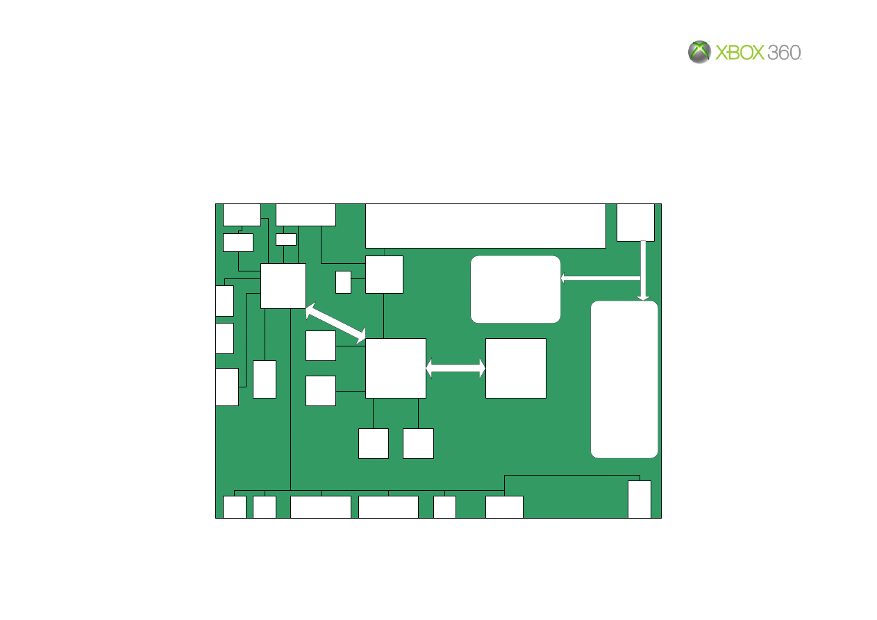
4. System Architecture
The block diagram below shows the main components of the XBOX360 motherboard in relation to
their position on the board.
CPU
GPU
North Bridge
(10MB embedded
DRAM)
RAM
RAM
RAM
RAM
South Bridge
SMC
ANA
LAN/USB
Connector
LAN
AV Connector
Audio
DAC
Clock
Gen
ROM
HDD
SATA
ODD
Pwr
ODD
SAT
A
Eject
Switch
IR
Rx
USB Memory
Connector
USB Memory
Connector
Binding
Button
Argon
Connector
USB
Game
Pad
Power
Supply
Connector
FAN ASSEMBLY
Front Side Bus
Bac
k S
ide B
us
GPU
Voltage Regulators
CPU
Voltage
Regulators
SPDIF
Microsoft Confidential
Page
7
of
35
Rev
1.0

5. Core Component Functionality
1. CPU
The XBOX360 has a custom central processing unit (CPU).
The CPU contains.
• 3 x 64 bit Power PC cores, each running at 3.2GHZ.
• 1 MB of shared L2 cache.
• The front side bus (FSB) consists of a 16 bit differential parallel bus in each direction.
• Transfer speed of the FSB is 5.4 GHz, giving a maximum data transfer rate of 10.8 GB/sec
simultaneously in the read and write direction.
Microsoft Confidential
Page
8
of
35
Rev
1.0

2. GPU / North Bridge
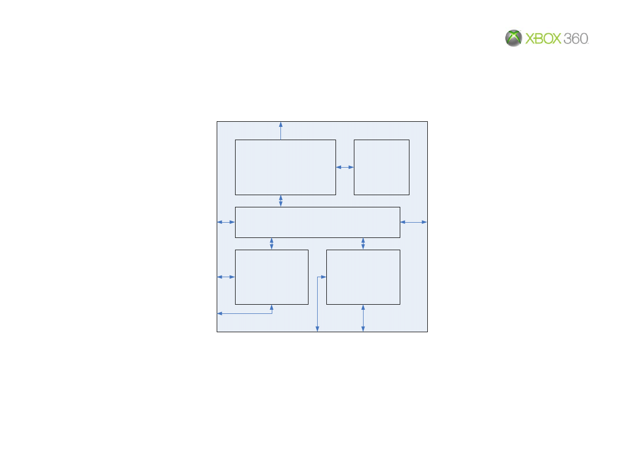
The XBOX360 has an integrated North Bridge, memory controller and graphics processing unit
(GPU) in a single package.
The GPU / North Bridge device contains the following features.
• The GPU has 10MB of embedded DRAM.
• The GPU generates a digital pixel output stream via the Xenon Digital Video Output bus
(XDVO) directly to the digital video encoder (ANA).
• The North Bridge contains the bus interface unit, which interfaces the Front Side Bus (FSB),
the Back Side Bus (BSB), the GPU and the memory bus.
• The North Bridge also contains 2 x 64 bit memory controllers for the RAM.
• The North Bridge is connected to the South Bridge via the Back Side Bus (BSB). This
consists of 4 PCI-Express busses, 2 read and 2 write, clocked at 2.5GHz.
Microsoft Confidential
Page
9
of
35
Rev
1.0
3. GPU / North Bridge Block Diagram
Bus Interface Unit
GPU
10MB
Embedded
DRAM
Memory
Controller
0
Memory
Controller
1
XDVO
Front
Side
Bus
Back
Side
Bus
RAM
Block
A
RAM
Block
B
RAM
Block
C
RAM
Block
D
Microsoft Confidential
Page
10
of
35
Rev
1.0

4. South Bridge / SMC
The XBOX360 South Bridge is the IO controller chip that contains interfaces to all the peripherals
and the System Management Controller (SMC).
The features include.
• Serial Advanced Technology Attachments (SATA) interfaces for the optical disc drive (ODD)
and the hard disc drive (HDD).
• Universal serial bus (USB) for the game pads, memory units and other peripherals such as a
WLAN adaptor.
• Media independent interface (MII) bus to the Ethernet control device.
• Digital audio output via the Inter IC Sound bus (I²S) to the audio DAC. Direct SPDIF output to
the AV connector.
• System interface to the flash ROM.
• Interface to the wireless transceiver located on the Argon board (USB).
• The system management controller (SMC) monitors the DVD tray state, AV mode, Argon
board (button and LED only), power good lines, reset done lines, infra red (IR) receiver for
the remote control, eject switch, binding button and the tilt switch.
Microsoft Confidential
Page
11
of
35
Rev
1.0

5. South Bridge / SMC Block Diagram
SMC
(8051)
System
Flash
Interface
Audio
Output
US
B
In
te
rf
a
c
e
PCI-Express
Control
Interface
LAN
MII
Interface
OD
D
SA
TA
HD
D
SA
T
A
Audio
DACs
SPDIF
AVIP
Ethernet PHY
USB
Memory Units
Controllers
Optical
Disc
Drive
Hard
Disc
Drive
Flash
Back
Side
Bus
To NB/GPU
IR
SMBUSx2
ANA
AVIP
Mode
Front Panel
DVD Tray
PSU
IR Remote
PWMx2
ANA
Microsoft Confidential
Page
12
of
35
Rev
1.0

6. ANA
ANA is short for the ANAlogue device.
The ANA contains.
• The digital video encoders for NTSC, PAL, HDTV and VGA standards.
• The digital to analogue converts (DACs) for the video output to the AV connector.
• The ANA monitors the temperature of the CPU, GPU, embedded DRAM and the air
temperature inside the console (Q1G3) then passes this information to the SMC via the
SMBUS.
• The twin independent fan driver circuits are controlled and monitored by the ANA.
• Power on reset generator and 12V detection circuit.
• Clock generator for the system, pixel and audio clocks.
Microsoft Confidential
Page
13
of
35
Rev
1.0

7. ANA Block Diagram
Digital
Video
Encoder
DAC
B
DAC
A
DAC
C
DAC
D
Fan
Driver
Op-Amps
Control
Interface
Temp
Sensor
Clock
Gen
Power
On
Reset
12V
Detect
ANA_XTAL_IN
27MHz
System
Clocks
External
Sensors
(diodes )
O/P Filters
AVIP Connector
Fan Driver O/P
Fan Feedback
PWM From SMC
Standby Power
SMC Reset
12V Detect
12V Power
Good
Pixel
Clock In
Video Syncs
Horiz / Vert
Digital Pixel
Data Bus
SMBUS
I2C
Pixel
Clock Out
Microsoft Confidential
Page
14
of
35
Rev
1.0

8. Random Access Memory
The XBOX360 uses a unified memory architecture to consolidate the system RAM and Graphics
RAM into a single memory pool.
• The system uses Graphics Double Data Rate Synchronous Dynamic Random Access
Memory (GDDR SDRAM).
• Each device has a data bus 32 bits wide.
• The memory is clocked at a speed of 800MHz; data is transferred using both clock edges
giving a data transfer speed of 1.6GHz.
• The system uses a 128 bit bus running at 1.6 Gb/sec. This provides a data transfer rate of
25.6 GB / sec.
• There are 2 x 64 bit memory controllers (0 / 1), each divided into 2 x 32 bit partitions (A&B /
C&D). This enables 4 memory devices (128 bit) to be accessed simultaneously.
Microsoft Confidential
Page
15
of
35
Rev
1.0

9. Power Supply Inputs
The XBOX360 Power supply unit is separate from the console and provides the conversion from
the AC line input to regulated DC voltages. The DC inputs to the motherboard are as follows.
• V_5P0STBY – 5V standby rail is active as long as the PSU is connected to the AC mains
supply.
• V_12P0 – Main 12V power rail which can be switched on / off (PSU_V12P0_EN) by the
system management controller (SMC) to bring the motherboard in and out of standby mode.
The motherboard can be switched from standby mode to full power mode by the following
methods.
• Main power button on the Argon board.
• Eject button on the ODD tray.
• Infra Red remote control.
• Wired or wireless controller port.
• External power on signal from the AV connector
Microsoft Confidential
Page
16
of
35
Rev
1.0

10. Standby Power Voltage Regulators
Local voltage regulation on the motherboard converts the 5V standby input from the PSU into
voltage supplies required by the motherboard for standby mode.
• V_3P3STBY (U5B1 pin 2) – 3.3V derived from V_5P0STBY.
• V_1P8STBY (U5B2 pin 2) – 1.8V derived from V_5P0STBY.
In standby mode the SMC, SMC clock generator, front panel button circuitry, the IR receiver
circuit, power on reset circuit (ANA), the wired and the wireless controller ports are all powered.
Note: V_5P0DUAL supplies the USB ports; this is derived from V_5P0STBY in standby mode and
V_5P0 in full power mode.
Microsoft Confidential
Page
17
of
35
Rev
1.0

11. Full Power Voltage Regulators
Once full power mode has been activated the SMC switches on the main 12V supply in the PSU
block via PSU_V12P0_EN. When the 12V power good signal from the ANA is received back by
the SMC, the following supply rails are activated in the following order.
• V_GPUCORE (L6C2 pin 2) – 2 phase switching circuit derived from V_12P0 and controlled
by U8N1– Nominally = 1.17V
• V_5P0 (U1E1 pin 3) – 5V regulator derived from V_12P0 and controlled by U4V1
• V_1P8 (U2T1 pin 2) – 1.8V regulator derived from V_5P0 controlled by U2T1 via U1E1
• V_MEM – 1.8V regulator derived from V_12P0 and controlled by U4V1
• V_3P3 (U1F1 pin 4) – 3.3V regulator derived from V_5P0
• V_SBPCIE (U3P1 pin 2) – South Bridge BSB supply derived from V_3P3
• V_GPUPCIE (U5C1 pin 2) – North Bridge BSB supply derived from V_3P3
• V_CPUCORE (L8E1 pin 2) – 3 phase switching circuit derived from V_12P0 and controlled
by U7U1 – Nominally = 1.21V
Microsoft Confidential
Page
18
of
35
Rev
1.0

12. Enable and Power Good lines
The SMC controls the power start up sequence by the following enable and power good lines.
These command and response signals occur in the following order.
• PSU_V12P0_EN – From the SMC to the PSU block (R8A2).
• ANA_V12P0_PWRGD – From the ANA to the SMC (U4B1 pin 122).
• VREG_GPU_EN_N – From the SMC to the GPU regulator (R9B1 then Q8B3 pin 3).
• VREG_GPU_PWRGD – From the GPU regulator (U8N1) to the SMC (R8N17/18).
• VREG_V5P0_EN_N – From the SMC to the 5V regulator (U4V1 pin 10).
• VREG_VMEM_EN_N – From the SMC to the VMEM regulator (U4V1 pin 11).
• VREG_V3P3_EN_N – From the SMC to the 3.3V regulator (R1F7/8 then U1F1 pin 3).
• VREG_CPU_EN – From the SMC to the CPU core regulator (U7U1 pin 11).
• VREG_CPU_PWRGD – From the CPU core regulator to the SMC (U7U1 pin 10).
Microsoft Confidential
Page
19
of
35
Rev
1.0

13. Clock signals
All of the XBOX360 clock signals are derived from a single 27MHz crystal (Y3B1).
In standby mode, the only clock running is the STBY_CLK (48MHz) from the clock generator
(U3B4) to the SMC.
During the Power on sequence the ANA_CLK_OE (R4B16/17) line is released by the SMC, this
starts the following clock signals simultaneously.
• CPU_CLK_DP/DN (R3C11/12) – 100MHz from the clock generator (U3B4) to the CPU.
• GPU_CLK_DP/DN (R3C7/8) – 100MHz from the clock generator (U3B4) to the GPU.
• PCIEX_CLK_DP/DN (R3C6/10) – 100MHz from the clock generator (U3B4) to the SB.
• SATA_ CLK_DP/DN (R3C2/4) – 100MHz from the clock generator (U3B4) to the SB.
• SATA_ CLK_REF (R3C27) – 25MHz from the clock generator (U3B4) to the SB.
• ENET_CLK (R3B8) - 25MHz from the clock generator (U3B4) to the LAN.
• ANA_PIX_CLK_DP/DN (R3C13/14) – 100MHZ from the ANA to the GPU.
• AUD_CLK (R3B15) – 24.576MHz from the ANA to the SB
From these the GPU generates the 800MHz memory clocks for the RAM devices and the SB
generates the I²S clocks for the Audio DAC (12.288MHz and 3.072MHz).
Microsoft Confidential
Page
20
of
35
Rev
1.0

14. Reset Lines
Once the SMC has received the “power good” signal from the CPU voltage regulator
(VREG_CPU_PWRGD), the following reset lines are released in the following order.
• ANA_RST_N (R3B1) – From the SMC to the ANA.
• SB_RST_N – From the SMC to the South Bridge.
• GPU_RST_N – From the SMC to the GPU.
• GPU_RST_DONE (R3P6/7) – From the GPU to the SMC.
• CPU_RST_N – From the SMC to the CPU.
• AUD_CLAMP (Q2N1 pin 2) – From the SMC to the audio clamp circuit.
Microsoft Confidential
Page
21
of
35
Rev
1.0
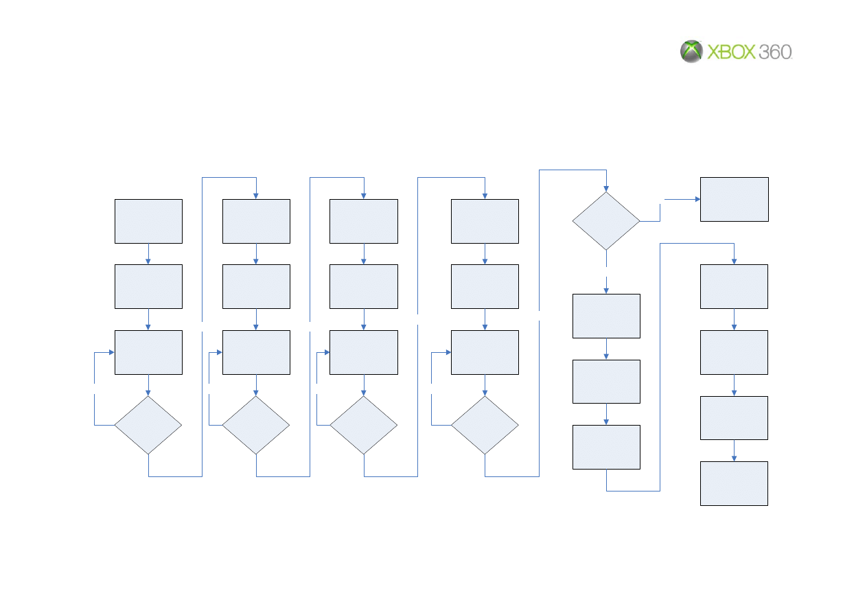
15. Boot sequence
AC Main Power
Connected
SMC Reset
Released
Monitor IR and
Buttons
SMC Sends
PSU_V12P0_EN
SMC Receives
ANA_V12P0_PW
RGD
Power On
Detected?
SMC Enables
VREG_GPU_EN_
N
Received
VREG_GPU_P
WRGD?
SMC Enables 5V,
Vmem and 3V3
Vregs
SMC Enables
ANA_CLK_OE
SMC Enables
VREG_CPU_EN
SMC Releases
ANA_RST_N
Received
VREG_CPU_P
WRGD?
SMC Releses
SB_RST_N
SMC Releases
GPU_RST_N
Received
GPU_RST_DO
NE?
SMC Releases
CPU_RST_N
Is The BSB
Trained?
CPU Runs 1
st
Boot Loader
CPU Runs 2
nd
Boot Loader From
Flash
2
nd
Boot Loader
sets up RAM
2
nd
Boot Loader
Copies 3
rd
Boot
Loader to RAM
3
rd
Boot Loader
Copies Kernel to
RAM
CPU Jumps to
Kernel in RAM
Yes
Yes
Yes
Yes
Yes
No
No
No
No
SMC Performs
Soft Reset
No
Microsoft Confidential
Page
22
of
35
Rev
1.0
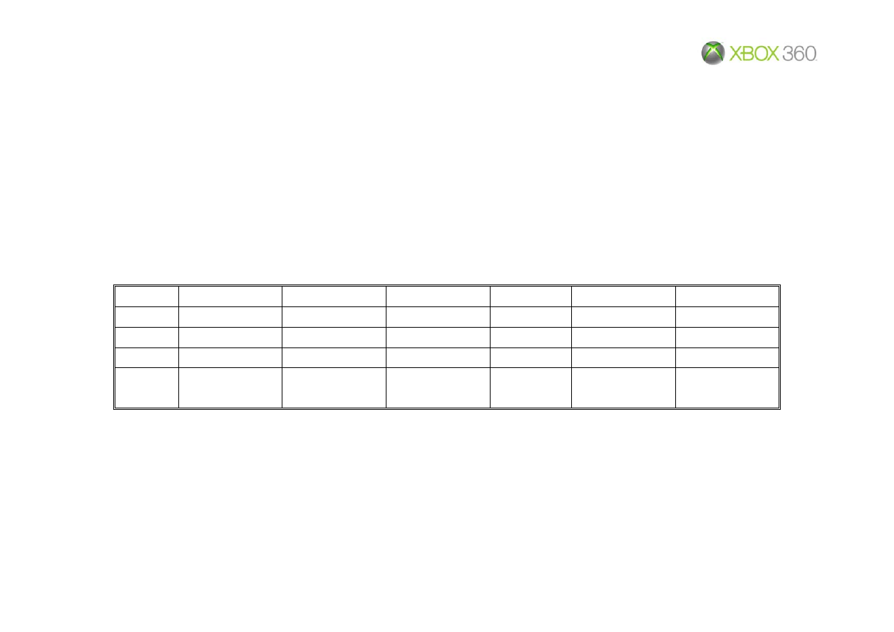
16. Analogue Video Output
The XBOX360 supports a number of video output standards including PAL, NTSC, HDTV and
VGA. The SMC monitors the video mode pins (AV_MODE0...2) on the AVIP connector (J2A1);
this informs the SMC of the type of AV cable that is fitted to the console.
The SMC can then configure the 4 DAC outputs from the video encoder via the SMBUS for the
appropriate outputs.
Standard
advanced
sdtv
hdtv
scart
vga
DAC A
N/A
Y (Luma)
Y (Luma)
Y (Luma) Green
Green
DAC B
N/A
C
(Chroma) Pr Pr
Red
Red
DAC C
N/A
N/A Pb
Pb
Blue
Blue
DAC D
CVBS
(Composite)
CVBS
(Composite)
CVBS
(Composite)
N/A
CVBS
(Composite)
CVBS
(Composite)
The DAC outputs can be monitored on L3A3 (A), L3A2 (B), L3A1 (C) and L2A1 (D).
Microsoft Confidential
Page
23
of
35
Rev
1.0
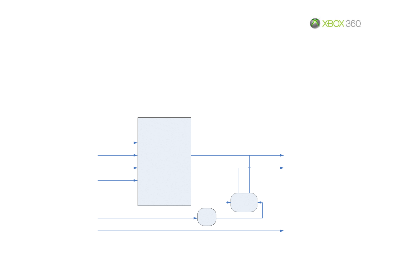
17. Audio output
Digital audio output from the South Bridge is transferred via the I²S bus to the audio Digital to
analogue converter (U2B1). The analogue audio output routes from the Audio DAC to the AV
connector.
Digital surround sound output (SPDIF) comes from the SB to the AV connector.
U2B1
Audio DAC
I2S_MCLK
I2S_BCLK
I2S_SD
I2S_WS
AUD_VOUTR
AUD_VOUTL
CR2N1
Q2N1
AUD_CLAMP
3
6
2
5
3
2
AUD_R_OUT
AUD_L_OUT
SPDIF
SPDIF
From
SMC /
South
Bridge
To
AVIP
Connector
Microsoft Confidential
Page
24
of
35
Rev
1.0
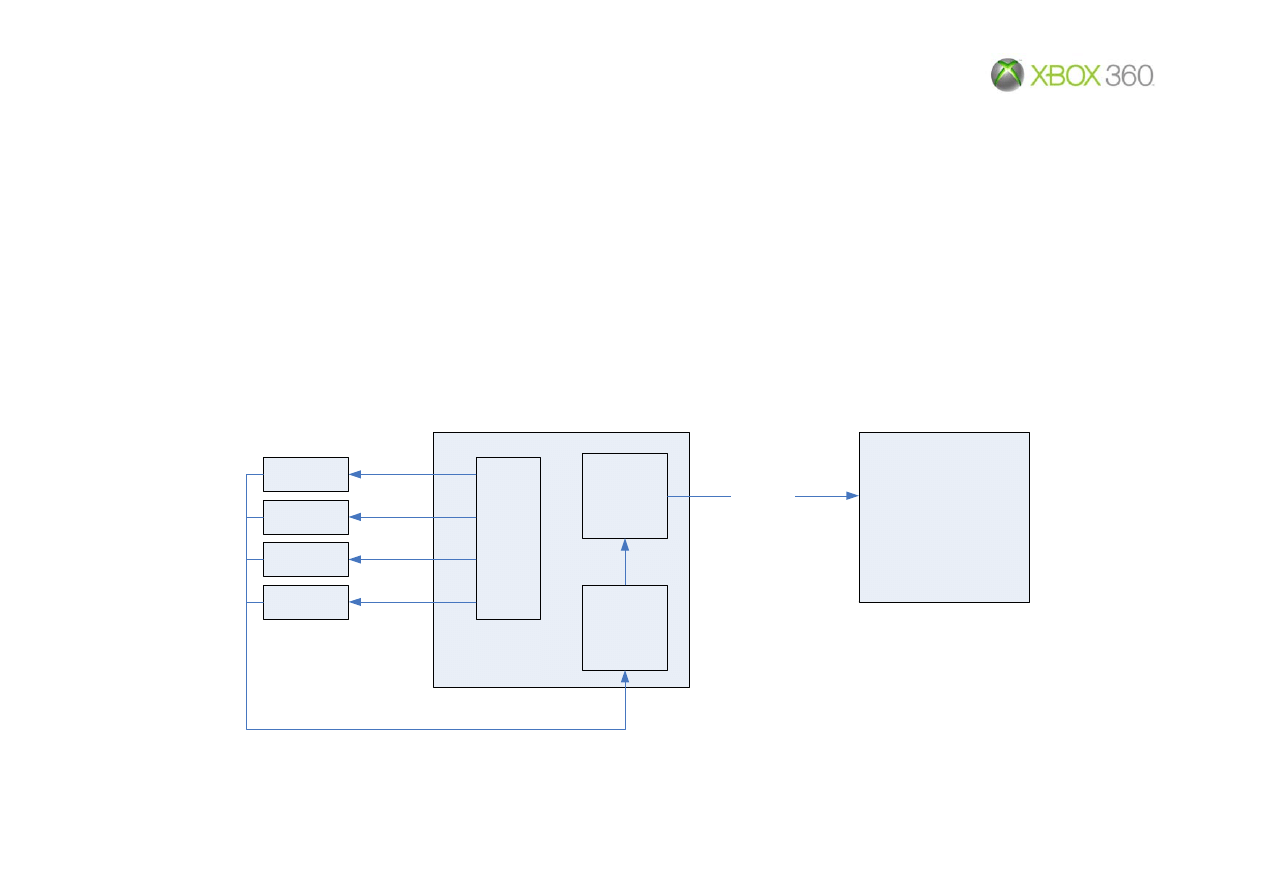
18. Temperature Monitoring
The XBOX360 has temperature diodes situated within the silicon of the CPU, GPU and the
EDRAM. The motherboard also has Q1G3 fitted to measure the internal air temperature of the
console.
The ANA multiplexes each temperature diode in turn; the voltage across each diode is measured
by an analogue to digital converter (ADC), and then transmitted to the SMC via the SMBUS (I²C
protocol).
ANA
MU
X
ADC
System
Management
Controller
CPU
GPU
EDRAM
Q1G3
I2C
Interface
SMBUS
Microsoft Confidential
Page
25
of
35
Rev
1.0
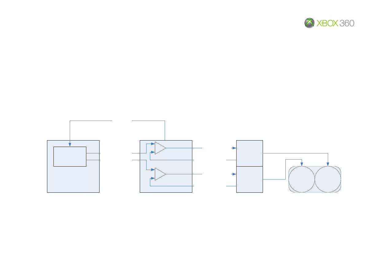
19. SMC Fan Control
The SMC calculates the appropriate speed for the two fans and drives two Pulse Width Modulated
(PWM) outputs to the ANA.
The PWM inputs to the ANA are converted into output voltages, proportional to the mark / space
ratios of the PWM inputs, and fed to the two fan drive circuits.
SMC
ANA
Fan
Control
1
Fan
Control
2
FAN
2
FAN
1
SMBUS
SMC_PWM0
SMC_PWM1
PWM
Generator
FAN2_FDBK
FAN1_FDBK
FAN1_OUT
FAN2_OUT
Microsoft Confidential
Page
26
of
35
Rev
1.0

20. Serial ATA bus, ODD and HDD
The XBOX360 has 2 Serial ATA busses, one for the optical disc drive (ODD) and one for the hard
disk drive (HDD). Each SATA bus has a differential pair of lines for both read and write.
The HDD connects to the motherboard via J1E1; this connector is used for power connections and
the serial data busses (Tx and Rx).
The ODD has two separate connections to the motherboard
• J1C1 – Serial data busses (Tx and Rx).
• J1D1 – ODD power and control (Tray status, Tray open and Eject switch).
Microsoft Confidential
Page
27
of
35
Rev
1.0

21. Ethernet
The XBOX360 contains a 10Mbit / 100Mbit Ethernet network port. Automatic polarity detection and
correction of RX channel provides peer to peer connectivity without the need for a hub or
crossover cable.
Connector: RJ45 with integrated LED indicators for link and activity status.
Green LED: illuminates when a network connection is established and will blink when there is
activity on the line.
Yellow LED: illuminates when the connection is established at 100Mbit and will not illuminate if
connected at 10Mbit.
Microsoft Confidential
Page
28
of
35
Rev
1.0

22. Debug LEDs
The XBOX360 XDK motherboards contain 4 debug LEDs. These LEDs are not fitted to retail
boards, but the test pads will still be driven. The LEDs indicate the following:
LED 0: BSB link indicator
• Off:
BSB not link trained
• Dim:
BSB trained in one direction only
• On:
BSB trained in two lane mode - This is the default
LED 1: Not used
LED 2: Power on retry count indicator. Number of resets that the SMC had to do to get the system
to transition from Standby to Full power. Only valid when LED 3 indicates Full On mode
• Off:
kernel booted first attempt – This is the default
• 1 flash:
kernel booted second attempt
• 2 flashes:
kernel booted third attempt
• 3 flashes:
kernel never performed SMC handshake within allotted timeout
Microsoft Confidential
Page
29
of
35
Rev
1.0

LED 3: Heartbeat indicator
• Standby:
Short
on,
long
off
• Standby to Full On transition:
Short on, short off
• Full
On:
Long
on,
Short
off
1
2
3
3
2
1
Standby Mode
Transition to Full On
Full On Mode
LED 3
Heartbeat
LED 2
Power Retry
LED 0
BSB Trained
Microsoft Confidential
Page
30
of
35
Rev
1.0

23. Argon Board
The Argon board supports the front panel power switch, the “ring of light” LEDs and the wireless
controller transceiver (2.4GHz Digital Enhanced Cordless Telecommunications (DECT)).
The Argon board is connected to the XBOX360 motherboard via J6G1.
The “Ring of Light” contains quadrants which glow to indicate areas of split screen control,
matching the “Ring of Light” around the XBOX360 button on the controllers. The tilt switch makes
sure that the “Ring of Light” is rotated when the consoles is stood vertically.
The Argon board communicates with the South Bridge via a USB bus, and the SMC via an I²C
bus.
Microsoft Confidential
Page
31
of
35
Rev
1.0

24. PCB Layout and Schematics Conventions
The XBOX360 uses the integrated component reference / PCB location designators for the
schematics and PCB layout. Top PCB designators 1A – 9G, bottom PCB designators 1M – 9V.
R2N10 is Resistor 10 in grid location
2N
Grid designations around
perimeter of MB
Microsoft Confidential
Page
32
of
35
Rev
1.0
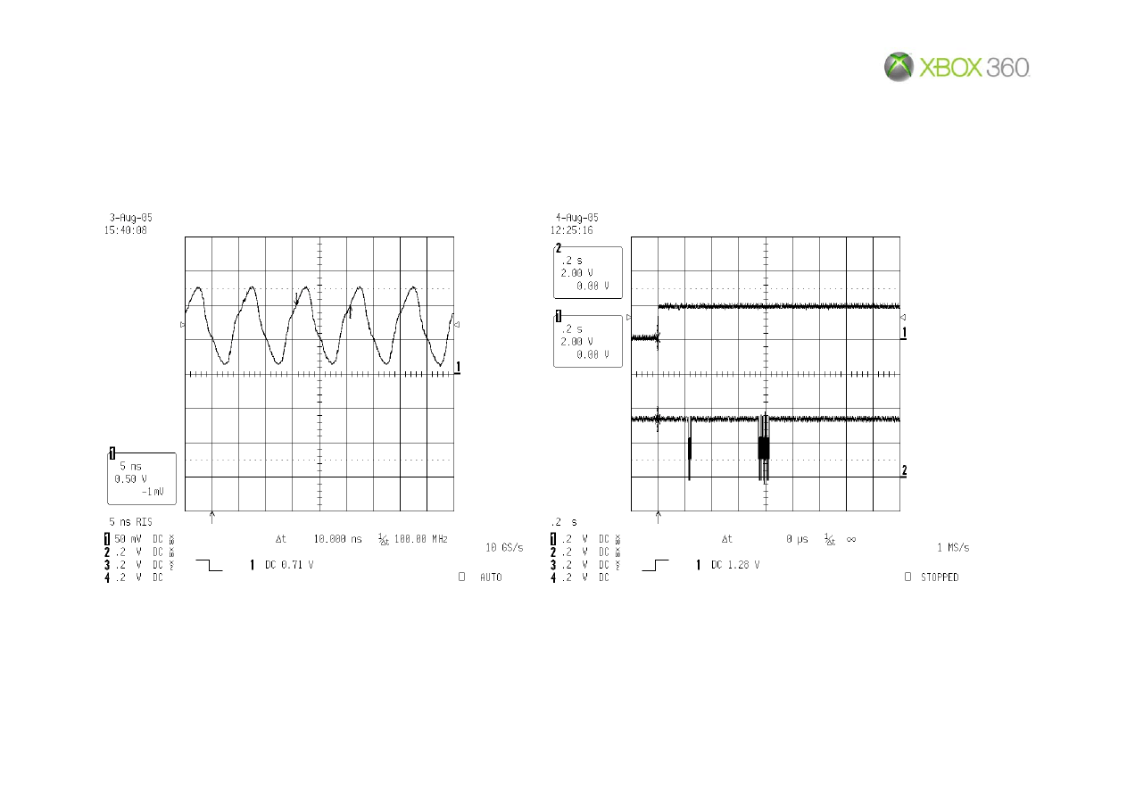
25. Oscilloscope Waveforms
1. CPU clock – 100MHz
1. CPU_RST
2. FLSH_CE
Microsoft Confidential
Page
33
of
35
Rev
1.0
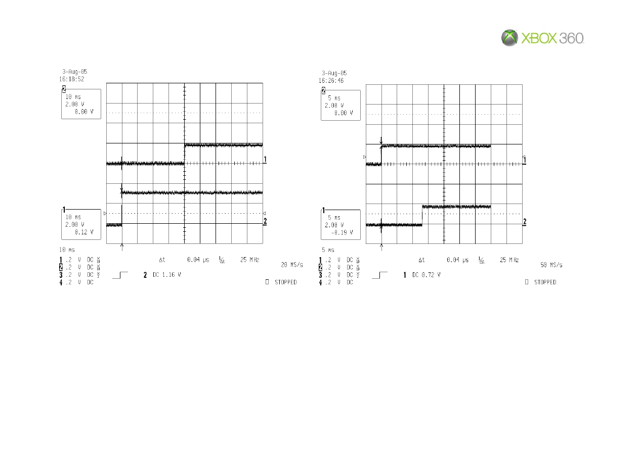
1.
GPU_RST
2.
ANA_RST
1.
GPU_RST
2.
GPU_RST_DONE
Microsoft Confidential
Page
34
of
35
Rev
1.0
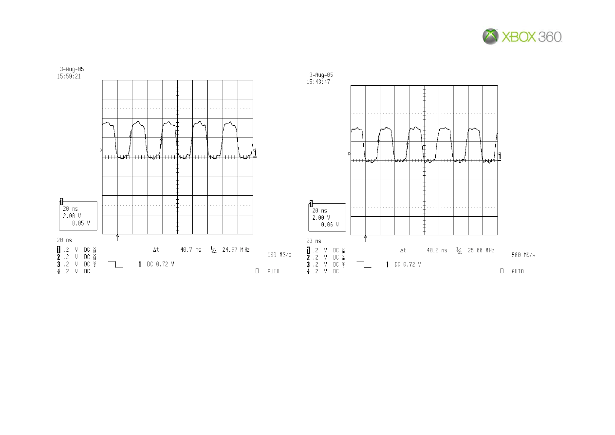
Audio
Clock
–
24.576MHz SATA
clock
reference
–
25MHz
Microsoft Confidential
Page
35
of
35
Rev
1.0
Wyszukiwarka
Podobne podstrony:
Theory of Operation
(ebook PDF)Shannon A Mathematical Theory Of Communication RXK2WIS2ZEJTDZ75G7VI3OC6ZO2P57GO3E27QNQ
Hawking Theory Of Everything
Maslow (1943) Theory of Human Motivation
Habermas, Jurgen The theory of communicative action Vol 1
Psychology and Cognitive Science A H Maslow A Theory of Human Motivation
Habermas, Jurgen The theory of communicative action Vol 2
Constituents of a theory of media
Luhmann's Systems Theory as a Theory of Modernity
Herrick The History and Theory of Rhetoric (27)
Adeptus Evangelion Base of Operations Record Sheet
Gardner The Theory of Multiple Intelligences
HUME AND?SCARTES ON THE THEORY OF IDEAS
Theory of Varied Consumer Choice?haviour and Its Implicati
Theory of literature MA course 13 dzienni
Krashen's theory of language learning and?quisition
więcej podobnych podstron