
Application Note 9021
A Novel IGBT Inverter Module for Low-Power Drive Applications
By M.K Kim, K.Y Jang, B.H Choo, J.B Lee, B.S Suh, T.H Kim
May, 2002
Rev. A, May 2002
1
Abstract - This paper presents a novel 3-phase IGBT module called the SPM (Smart Power
Module). This is a new design developed to provide a very compact, low cost, high perfor-
mance and reliable motor drive system. Several distinct design concepts were used to achieve
the highly integrated functionality in a new cost-effective small package. An overall description
to the SPM is given and actual application issues such as electrical characteristics, circuit con-
figurations, thermal performance and power ratings are discussed.
I. Introduction
The terms “energy-saving” and “quiet-running” are becoming very important in the world of
variable speed motor drives. Inverter technology is being increasingly accepted and used by a
wide range of users in the design of their products.
For low-power motor control, there are increasing demands for compactness, built-in control,
and lower overall-cost. An important consideration, in justifying the use of inverters in these
applications, is to optimize the total-cost-performance ratio of the drive system.
In order to meet these needs, we have designed and developed a new series of compact,
highly functional and very efficient power semiconductor devices called the “SPM (Smart
Power Module)”. Fig. 1-(a) shows a real photograph of the SPM. SPM-inverters are a very via-
ble alternative to conventional ones for low-power motor drives due to their attractive charac-
teristics, specifically for appliances such as washing machines, air-conditioners etc. This
paper describes in detail the design issues, electrical performance, and other important con-
siderations for designing the system.
Fig. 1 Photograph of the SPM and the internal function block diagram
D rive C ircuit
Thermistor
D rive C ircu it
U VL O
L eve l-S hift
In p ut C ircu it
D rive C ircu it
U V LO
L eve l-S hift
In pu t C ircu it
D rive C ircuit
U V LO
L eve l-S hift
In p ut C ircu it
In p ut C ircu it
FO Lo g ic
U V P ro te ction
S C P ro te ction
V
B(U)
VFO
P
Nu
Nv
Nw
U
V
W
Rsc
Vcc
GND
Csc
V
B(V)
V
B(W)
Vs(u)
Vs(v)
Vs(w)
IN(WH)
IN(VH)
IN(UH)
IN(UL,VL,WL)
Rth
Vth
CFOD
(b) Internal function block diagram
(a) Photograph of the SPM
mm
60
mm
31

2
Rev. A, May 2002
II. Description Of Design and Function Features
A. Features
The SPM combines optimized circuit protection and a drive that are matched to the IGBT's
switching characteristics. The SPM is composed of three normal IGBTs, three sense IGBTs,
three HVICs, one LVIC and one thermistor as shown in Fig. 1-(b). Highly effective short-circuit
current detection/protection is achieved through the use of advanced current sensing IGBTs
that allow continuous monitoring of the IGBT current. System reliability is further enhanced by
the built-in over-temperature and integrated under-voltage lockout protection. The high speed
built-in HVIC provides an opto-coupler-less IGBT gate driving capability that further reduces
the overall size of the inverter system design. The HVIC facilitates the use of a single-supply
drive topology. This allows the SPM to be driven by only one drive supply voltage without a
negative bias. The SPM has three divided negative DC terminals to monitor the inverter output
current by using three shunt resistors. Nowadays, the sensorless controlled inverter systems
are widely used because of the advantages in drive cost, reliability and signal noise immunity.
The SPM incorporates these terminals in order to provide a low-cost sensorless control solu-
tion [3].
B.Protective functions
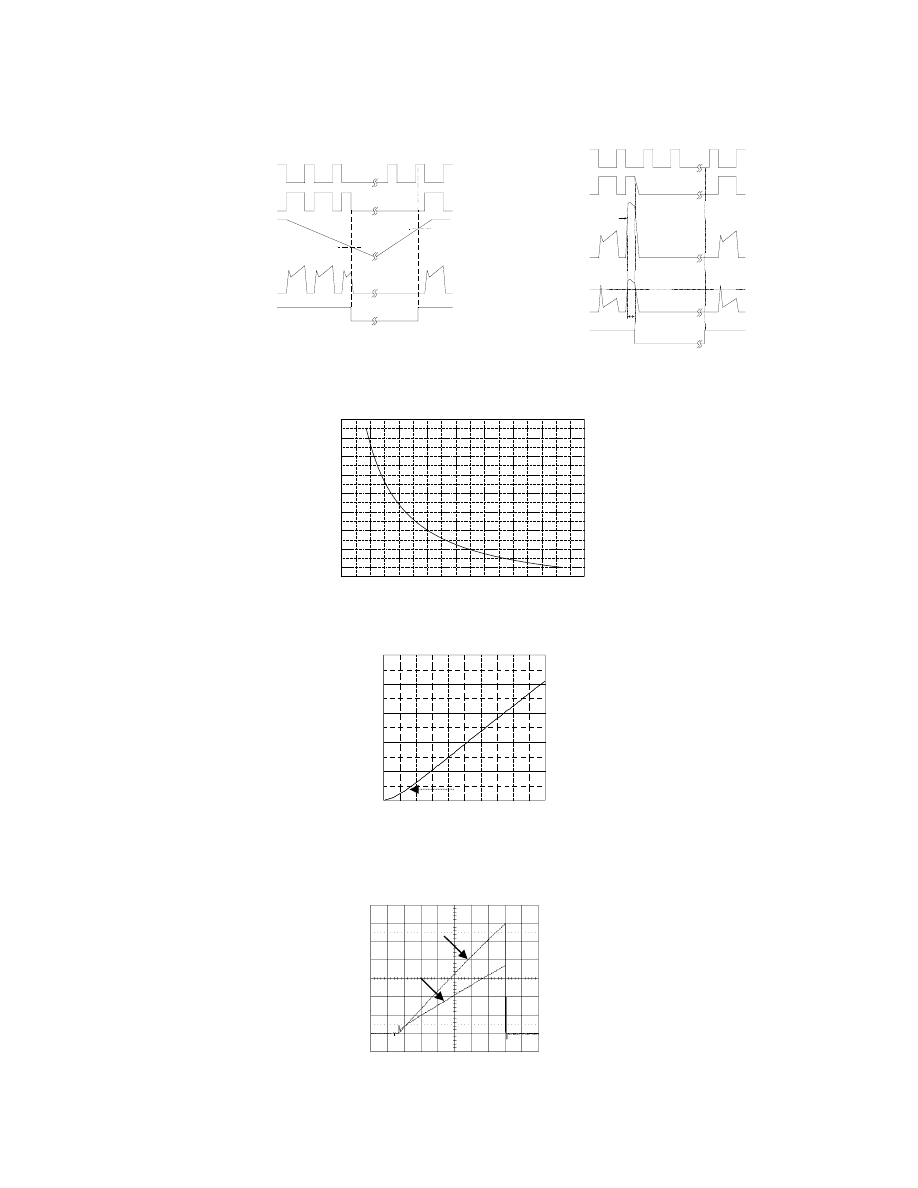
The SPM provides two main protective functions. One is control supply under-voltage protec-
tion and the other is short-circuit current protection. The principles of operation of these pro-
tective functions are described in the timing diagram in Fig. 2. When the control supply voltage
drops under its UV detect level, the internal gating signal is blocked and a fault-out signal is
generated. Once the supply voltage rises again over the UV reset level, the fault-out signal
becomes high and the SPM is operated by the command signals. The LVIC of the SPM
detects the low-side collector current level by monitoring the sensing voltage. In the case of a
short-circuit, the SPM shuts down the internal gating signal and generates a fault-out signal.
This current sensing method provides a simplified and cost-effective solution. The sense-IGBT
has very linear sensing characteristics in the range of approximately above 15% of the rated
current as shown in Fig. 4. Fig. 5 shows the real sensing voltage waveform. The sensing resis-
tor, Rsc, can be selected to determine the trip current level which can be optimized according
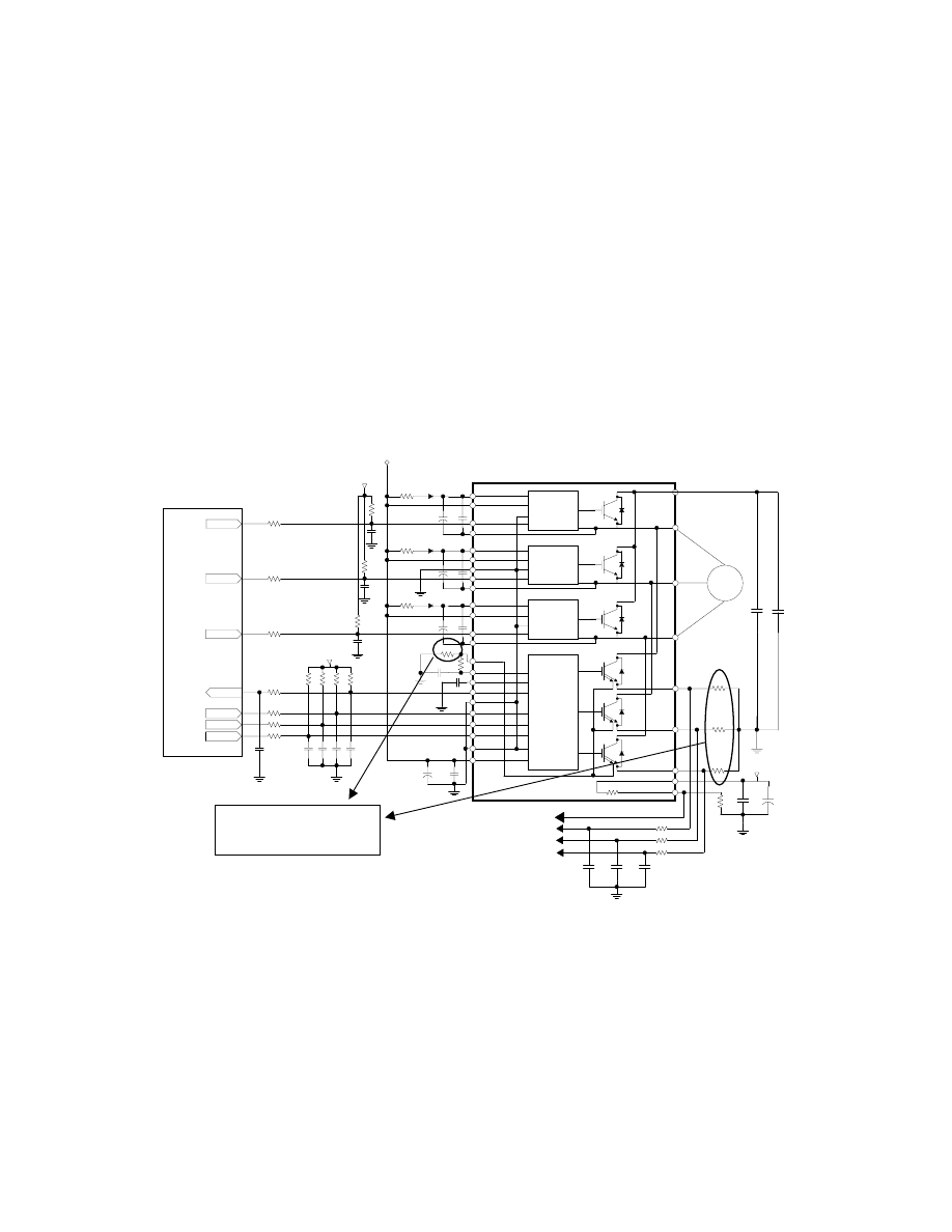
to the field requirements. Refer to the overall application circuit of Fig. 11, which shows the
Rsc and Rs parameters related to the short-circuit protection function. Fig. 3 and (1) show the
relationship between the sensing resistor Rsc and the desired trip current Isc when the shunt
resistor Rs is zero.
DUT: FSAM15SH60
where, I
SC
: Circuit trip current [A]
R
SC
: Sensing resistance [
Ω]
I
C
: Rating current of DUT [A]
I
SC
82
I
C
Rating Current
(
)
R
SC
----------------------------------------------
×
=
1
( )
Rev. A, May 2002
3
Fig. 2 Time chart of under-voltage and short-circuit protection
Fig. 3 The relationship between short-circuit trip current (I
SC
) and sensing resistor (R
SC
)
Fig. 4 Sensing characteristics of the sense-IGBT
Fig. 5 Measured voltage in the sensing resistor, Rsc. Where,
(1) Collector current (5A/div.) (2) Rsc voltage (0.2/div.)
Internal IGBT
Gate-Emitter Voltage
Input Signal
Output Current
Sensing Voltage
Fault Output Signal
P1
P2
P3
P4
P6
P5
P7
P8
SC Reference
Voltage (0.5V)
RC Filter Delay
SC Detection
Internal IGBT
Gate-Emitter Voltage
Input Signal
Output Current
Fault Output Signal
Control Supply Voltage
P1
P2
P3
P4
P6
P5
UV
detect
UV
reset
(a) Unter-voltage protection
(b) Short-circuit protection
10
20
30
40
50
60
70
80
90
10
20
30
40
50
60
70
80
90
SC T
rip
Cur
rent
I
SC
[A
]
Sensing Resistor R
SC
[
Ω
]
0.0
0.1
0.2
0.3
0.4
0.5
0
5
10
15
20
25
I
C
[A
]
V
SC
[V]
15% of the
rating current
(1)Ic
(2)Vsc
[10
µs/Div]
4
Rev. A, May 2002
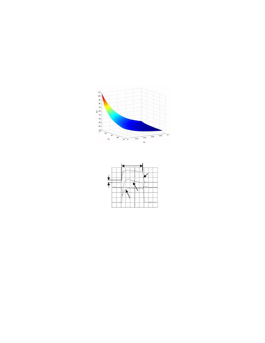
The circuit trip current, I
SC
level is in inverse proportion to the R
SC
value as shown in (1). We
can see that the trip current level corresponding to the Rsc of 56 is 150% of the rated current.
I
SC
level also decreases along with the increasing of the shunt resistor R
S
. In case both Rsc
and Rs are used, the relationship is shown in Fig. 6. Fig. 7 shows the actual waveforms under
a short-circuit protecting situation with Rs=0
Ω. The Rsc voltage increases as the low-side
IGBTs collector current increases. Once the Rsc voltage in Fig. 11 reaches to 0.5V, the LVIC
shuts down the gating signal after time delay of about 4.5
µs, which is mainly caused by a low-
pass filter composed of Csc and Rf as shown in Fig. 11. Note that we wanted to detect 150%
load current, with Rsc of 56
Ω, which is around 24A, while using a 15A rated SPM.
Fig. 6 Short-circuit trip current (I
SC
) related to sensing resistance (R
SC
)
and shunt resistance (R
S
)
Fig.7 Waveforms for short-circuit protection. Where
(1) Rsc voltage (1V/div.) (2) V
CE
(100V/div.)
(3) Collector current (20A/div.)
C. Boot-Strap Circuit
The level-shift feature integrated within the HVIC provides the advantage of an opto-coupler-
less control interface for the high-side IGBTs drive. Hence, it is possible to operate all six
IGBTs within the SPM using only one drive supply of 15V without a negative bias. To achieve
this, some passive components such as capacitors, diodes and resistors should be used
externally. The principle of operation of the bootstrap circuit is described in Fig. 8. The voltage
source of the bootstrap capacitor is the V
CC
supply. Its capacitance is determined by the fol-
lowing constraints
(1) The gate charge required to enhance the IGBT
(2) I
QBS
– Quiescent current for the HVIC
(3) Currents within the level shifter of the HVIC
(4) Bootstrap capacitor leakage current
4.5
µs
(1)Rsc
(2)V
CE
(3)Ic
[1
µs /Div]
0.5V

Rev. A, May 2002
5
Factor 4 is only relevant if the bootstrap capacitor is an electrolytic capacitor. It can be ignored
if other types of capacitors are used. Hence, it is always better to use a non-electrolytic capac-
itor if possible. The following equation describes the minimum charge, that needs to be sup-
plied by the bootstrap capacitor.
where, Q
g
= Gate charge of the high-side of the IGBT
f = Switching frequency
I
CBS(leak)
= Bootstrap capacitor leakage current
I
QBS(max)
= Maximum quiescent current for the HVIC
Q
ls
= Level shift charge required per cycle = 5nC
Fig. 8 The bootstrap circuit operation and time chart
The bootstrap capacitor must be able to supply this charge (Q
BS
), and retain its full voltage.
Otherwise, there will be a significant amount of ripple on the V
BS
voltage, which could fall
below the VBSUV (under-voltage detection level). Hence, it is recommended that the charge
in the C
BS
capacitor be at least twice the above value. Due to the nature of the bootstrap cir-
cuit operation, a low value capacitor can lead to overcharging, which could in turn damage the
HVIC. Hence, to minimize the risk of overcharging and further reduce the ripple on the V
BS
voltage, it is recommended that the C
BS
value be multiplied by a factor of 15. The minimum
bootstrap capacitor value can be obtained from (3). Note that the following (4) should be used
for a specific system application, with an extended period of application of the standstill mode
of the PWM output, during the changing of the rotor direction. It can occur in washing machine
drive applications where the voltage of V
BS
can be lowered to an under-voltage protection
level.
where,
∆V = the allowable discharge voltage of the C
BS.
where,
∆t = the period of standstill mode and all of the IGBTs are in turn-off state.
The C
BS
capacitor only charges when the high-side of the device is off and the V
S
voltage is
pulled down to ground. Therefore, the on-time of the low-side IGBT must be sufficient to
ensure that the charge drawn from the C
BS
capacitor can be fully replenished. Hence, inher-
ently there is a minimum on-time of the low-side IGBT (or off-time of the high-side IGBT).
Q
BS
2Q
g
I
QBS max
(
)
f
----------------------- Q
ls
I
CBS leak
(
)
f
-----------------------
+
+
+
≥
2
( )
Vcc
IN
COM
VB
HO
VS
Vcc
IN
COM
Out
Vin(L)
+
Vdc
-
V
BS
V
CC
V
in(L)
V
PN
0V
0V
V
S
ON
C
BS
15
2 2Q
g
I
QBS max
(
)
f
----------------------- Q
ls
I
CBS leak
(
)
f
-----------------------
+
+
+
∆V
---------------------------------------------------------------------------------------------
×
≥
3
( )
C
BS
I
QBS max
(
)
∆t
×
∆V
-----------------------------------
≥
4
( )
6
Rev. A, May 2002
III. Structure and Packaging
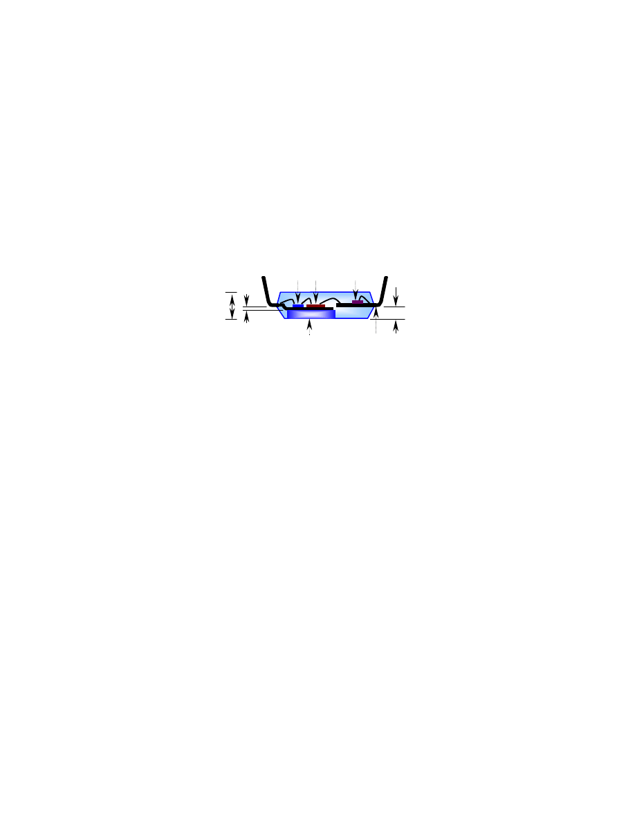
The narrow space multi-die attach technology is used in the SPM. This results in reduced
noise, size and less mutual interference. The package is designed to guarantee the best heat
transfer from the power chips to the outer heat-sink by using the Ceramic-Pad attaching tech-
nology. The ceramic-attached lead frame that includes all the power chips and ICs is transfer
molded with good insulation and high conductivity materials. This allows for low cost, high
thermal performance. The lead frame structure has a 1mm down-set shape. This makes the
thermal resistance low but doesn't reduce the distance between lead frame and the outer
heat-sink. More down-set thickness affects the reliability and assembly process. The optimiza-
tion of the bending depth has been obtained by doing simulations and experimental tests. The
total thickness of the molding is 7.2mm and the ceramic thickness is 2mm. Fig. 9 shows the
cross sectional structure of the SPM.
Fig. 9 Cross sectional structure of SPM (unit: mm)
3.0
IGBT
FRD
IC
Lead
Frame
Ceramic
1.0
7.2
Rev. A, May 2002
7
IV. Electrical Characteristics and Performance
A. Electrical Characteristics
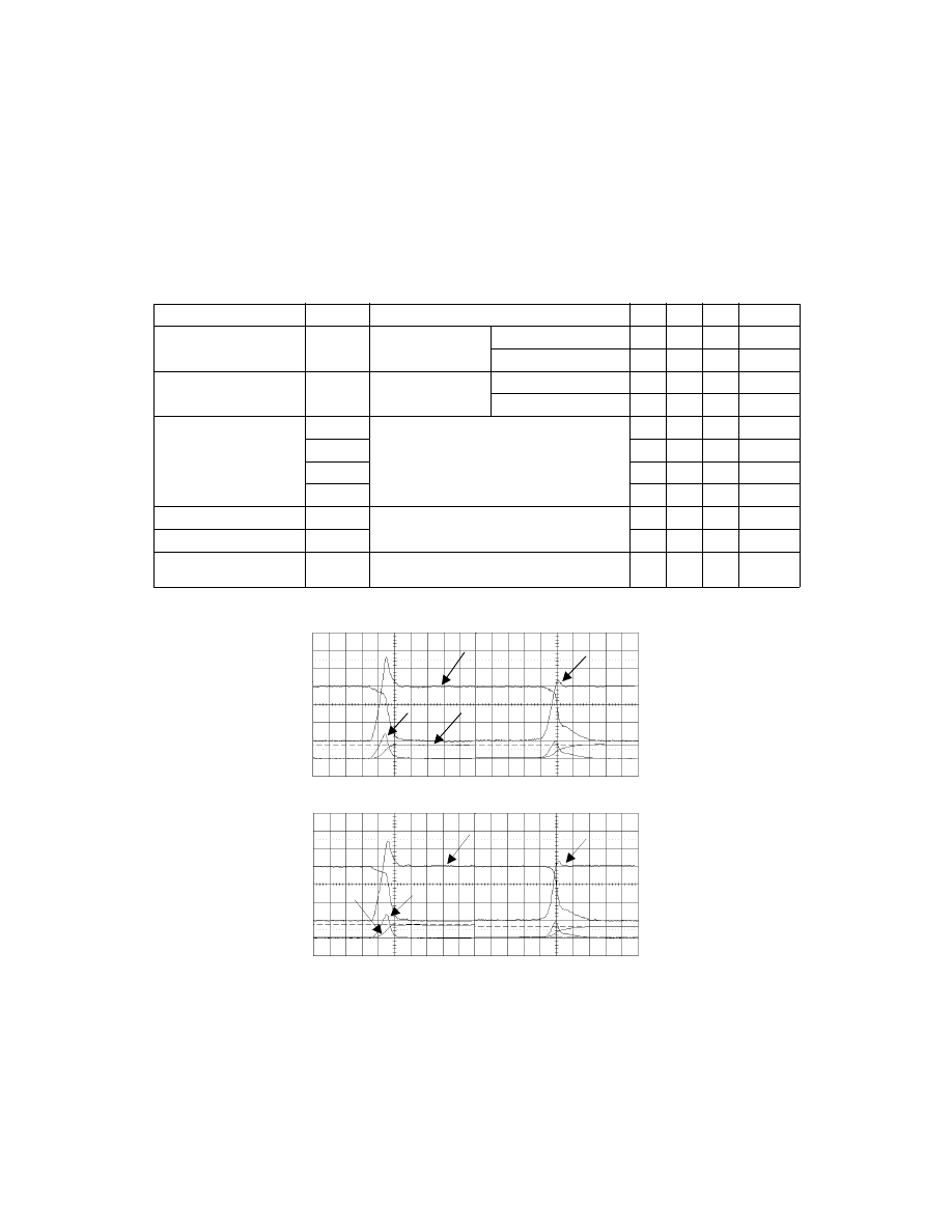
Table 1. shows the basic electrical characteristics of the FSAM15SH60. The table also
includes the switching loss data at Tj of 125°C condition. This will be utilized for calculating the
SPM power loss. Fig. 10 is the switching waveforms of high-side, low-side IGBTs of the SPM
under conditions shown in Table 1.
Fig. 10 High/Low side IGBT switching waveforms at Tj = 25
°C
Where, (1) Ic (5A/div.) (2) V
CE
(100V/div.)
(3) Switching power loss(4kW/div.)
(4) Switching energy (0.5mjoule/div.)
Table 1: Electrical characteristics of the SPM
Item
Symbol
Condition
Min. Typ. Max.
Unit
Collector-emitter
V
CE(sat)
V
CC
= V
BS
= 15V
I
C
= 15A, T
j
= 25°C
-
-
2.5
V
Saturation Voltage
V
IN
= 0V
I
C
= 15A, T
j
= 125°C
-
-
2.6
V
FWDi Forward Voltage
V
FM
V
IN
= 5V
I
C
= 15A, T
j
= 25°C
-
-
2.5
V
I
C
= 15A, T
j
= 125°C
-
-
2.3
V
Switching Times
t
ON
V
PN
= 300V, V
CC
= V
BS
= 15V
-
0.34
-
us
t
C(ON)
I
C
= 15A, T
j
= 25°C
-
0.15
-
us
t
OFF
V
IN
= 5V
↔ 0V, Inductive Load
-
0.58
-
us
t
C(OFF)
(High/Low-side)
-
0.25
-
us
Turn-on switching loss
E
SW(ON)
Same as Switching Times except
T
j
= 125°C
0.37
mj/pulse
Turn-off switching loss
E
SW(OFF)
0.34
mj/pulse
Collector-emitter
Leakage Current
I
CES
V
CE
= V
CES
, T
j
= 25°C
-
-
250
uA
(a) High-side on/off switching waveform (100ns/div.)
(b) Low-side on/off switching waveform (100ns/div.)
(1)
(2)
(3) (4)
(1)
(2)
(3)
(4)
8
Rev. A, May 2002
B. Application Circuit and Design
The circuit configuration for a typical application of the SPM is shown in Fig. 11. A single-sup-
ply 15V drives the low-side IGBTs directly and charges the bootstrap circuitry for the HVICs.
The LVIC blocks the command signals from the controller and generates a fault signal when a
failure mode, the SC current failure or the supply under-voltage failure, is detected. The V
FO
output is of the open-collector type. This signal line should be pulled up to the positive side of
the 5V power supply with approximately 4.7k
Ω. In the short-circuit protection circuit, the selec-
tion of the R
F
C
SC
time constant in the range of 3~4us is recommended. RF should be at least
30 times larger than R
SC
. The integrated 5V CMOS/TTL compatible Schmitt trigger input con-
ditioning circuit enables direct interface with a microprocessor. The high-side input is pulled up
to +5V with a 1.5M
Ω resistor and the low-side input is pulled up to V
CC
with a 100k
Ω resistor
as shown in Fig. 12. When the driver part of the gate signal is composed of an open-collector,
an appropriate pull-up resistor can be selected. When the driver part is composed with push-
pull buffer, the low-side pull-up resistor is recommended to be under 2
Ω when V
CC
is +15V. In
order to increase the noise immunity, a pull-down capacitor can be used. The capacitances
are recommended to be 1.2nF for the high-side and 0.47nF for the low-side.
Fig. 11 Typical application circuit example
C O M (L)
VC C
IN (UL)
IN (VL)
IN (W L)
VF O
C (FO D )
C (SC )
O U T(U L)
O U T(VL)
O U T(W L)
N
U
(26)
N
V
(27)
N
W
(28)
U (29)
V (30)
W (31)
P (32)
(23) V
S(W )
(22) V
B(W )
(19) V
S(V)
(18) V
B(V)
(9) C
SC
(8) C
FOD
(7) V
FO
(5) IN
(W L)
(4) IN
(VL)
(3) IN
(UL )
(2) COM
(L)
(1) V
CC(L)
(10) R
SC
V
TH
(25)
R
TH
(24)
(6) COM
(L)
VC C
VB
O U T
C O M
VS
IN
VB
VS
O U T
IN
C O M
VC C
VC C
VB
O U T
C O M
VS
IN
(21) V
CC(W H)
(20) IN
(W H)
(17) V
CC(W H)
(15) IN
(W H)
(16) COM
(H)
(14) V
S(U)
(13) V
B(U)
(12) V
CC(UH)
(11) IN
(UH)
F ault
15V line
C
BS
C
BSC
R
BS
D
BS
C
BS
C
BSC
R
BS
D
BS
C
BS
C
BSC
R
BS
D
BS
C
SP15
C
SPC15
C
FOD
5V line
R
P
C
PL
C
BPF
R
P
R
P
R
P
C
PL
C
PL
5V line
C
PH
R
P
C
PH
R
P
C
PH
R
P
R
S
R
S
R
S
R
S
R
S
R
S
R
S
M
Vdc
C
DC S
5V line
R
TH
C
SP05
C
SPC05
THERM ISTOR
Temp. Monitoring
G ating UH
G ating VH
G ating W H
G ating W H
G ating VH
G ating UH
C
PF
C
C
C
C
P
P
P
P
U
U
U
U
R
FU
R
FV
R
FW
R
SU
R
SV
R
SW
C
FU
C
FV
C
FW
U-Phase Current
V-Phase Current
W -Phase Current
R
F
C
SC
R
SC
Resistors related with
short-circuit protection

Rev. A, May 2002
9
Fig. 12 Example of a pulling-up at a direct connection to a microprocessor
C.Thermal Performance and Operation Ratings
The power carrying potential of a device is dependent on the heat transfer capability of the
device. The SPM provides not only good thermal performance but also operating frequency
options in accordance with the application.
1. Thermal resistance
For a heat-sink attached device, the major thermal path between its thermal network is the
'junction-to-case-to-heat-sink-to-ambient' path. The junction-to-case thermal resistance R
θjc
is
the measurement of heat flow between the chip junction and the surface of the package. R
θjc
can be represented by the following equation.
where, P(W): Power dissipation per device
T
j
(
°C): Junction temperature
T
c
(
°C): Case reference temperature
Since Tc and P can be measured directly, the only unknown constant is the junction tempera-
ture Tj. The Electrical Test Method (ETM) is widely used to measure the junction temperature.
The ETM is a test method using the relationship between the junction temperature and the
Temperature Sensitive Parameter (TSP). Usually, the thermal characteristics of these parame-
ters are an intrinsic electro-thermal property of semiconductor junctions. For example, the for-
ward-biased voltage drop of a diode and the saturation voltage of an IGBT are such
parameters. Once the relationship between Tj and TSP is obtained, the thermal resistance
(R
θjc
) can be measured. The heating current and TSP-measurement current are alternately
applied to the device. The time chart of the duration is shown in Fig. 13. The TSP sampling
time must be very short so as not to allow any appreciable cooling of the junction prior to re-
applying the heating power. Tj can be obtained in this process using the known relationship
between the junction temperature and the TSP. Once Tj reaches thermal equilibrium, its value
along with the reference temperature Tc and applied power P is recorded. Using the measured
values and (5), the junction-to-case thermal resistance R
θjc
can be estimated. After obtaining
R
θjc
, it can be used for various thermal analyses. For example, one can predict the junction
temperature Tj in a field condition using the following equation
M icroprocessor
+5V
Vcc
SPM
High side : 1.5M
Ω
Low side : 100
k
Ω
Rh
R
θjc
T
j
T
c
–
P
----------------
=
5
( )
T
j estimated
(
)
R
jc
P T
c
+
×
=
6
( )

10
Rev. A, May 2002
It can also be used for calculating the device power loss and for the selection of a heat-sink.
From the measurement result, the typical value of the thermal resistance of FSAM15SH60 is
2.0°C/W
Fig. 13 Thermal resistance test timing chart
2. SPM power losses and ratings
The total power loss in the SPM is composed of conduction and switching losses caused in
the IGBTs and FRDs. The loss during the turn-off steady-state can be ignored because it is a
very small amount and has little effect on increasing the temperature in the device. The con-
duction loss depends on the DC electrical characteristics of the device i.e. saturation voltage.
Therefore, it is a function of the conduction current and the device's junction temperature. On
the other hand, the switching loss is determined by the dynamic characteristics like turn-on/off
time and over-voltage/current. Hence, in order to obtain the accurate switching loss, we
should consider the DC-link voltage of the SPM system, the applied switching frequency and
the power circuit layout in addition to the current and temperature. For the detailed equations
for calculating both conduction and switching losses based on a PWM-inverter system for
motor control applications, refer to the references [4] and [5].
The typical forward characteristics of an IGBT and a diode can be measured by curve tracer
equipment. Assuming that the switching frequency is high, the output current of the inverter
can be considered as a sinusoidal one. That is,
where f is a phase-angle difference between voltage and current. Using (7), the conduction
loss of one IGBT and diode can be obtained. The switching energy loss Eon and Eoff can be
measured by the switching waveform of a device. The switching loss depends on the IGBT
and diode dynamic characteristics. The turn-off loss depends on the speed of the gate drive
and the IGBTs current tail due to the recombination of minority carries. The turn-off energy is
measured indirectly by multiplying the current and voltage and integrating them over time. The
turn-on loss is due to the rate of current change and the stored charge in the free wheel diode.
The loss is measured using the same method. For the calculation of switching loss, the linear
dependency of a switching energy loss on the switched current is assumed from the measure-
ment result. The total inverter conduction losses are six times the Pcon of the IGBT and diode
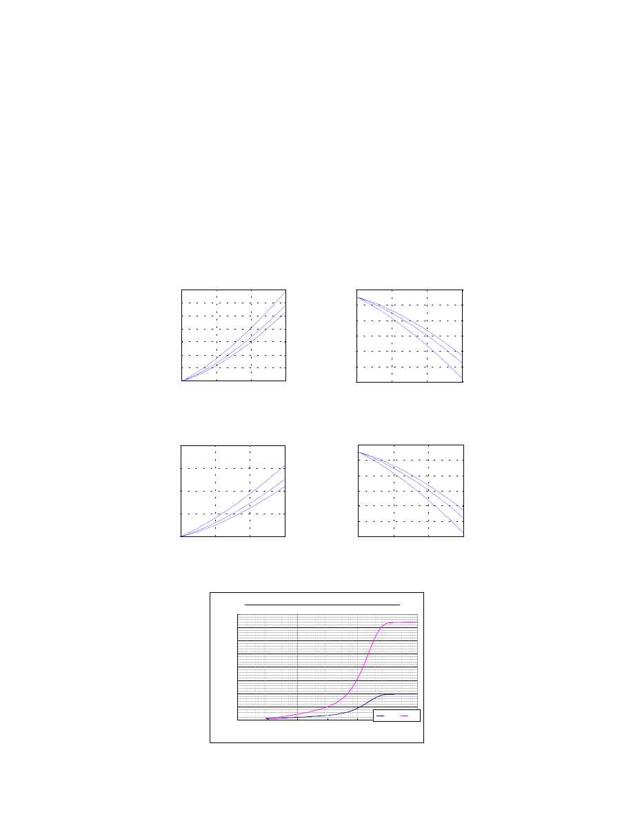
conduction losses. Fig. 14-(a) shows the calculated results including the total power loss due
to conduction and switching in the IGBTs and FRDs. The results are obtained by using a high
speed SPM device such as the FSAM15SH60. It should be noted that the PWM modulation
index MI = 0.8 and cosf=0.8 are used as common parameters in all the calculations. Figs. 14-
(a) and 15-(a) show the power losses caused in the SPMs up to a rating current of 15A
depending on the rms motor current variation. Fig. 14 shows the SPM power losses and
acceptable maximum heatsink temperature to restrict the device's junction temperature below
125°C at 300V of DC-link voltage. Fig. 15 shows a DC-link voltage of 400V. We can see that
the difference of about 24% is in the power rating between 15kHz and 3kHz operating condi-
tions. Fig. 16 shows a thermal impedance, which is the thermal resistance between junction
and ambient air. The heat-sink used is shown in Fig. 17.
Heating interval
M easurment
interval
Heating
power
Time
i
I
peak
θ φ
–
(
)
cos
=
7
( )
Rev. A, May 2002
11
When the DC-link voltage is 300V and Irms is 5A, the IGBT's power loss and FRD's power
loss is 4.8W and 1.2W respectively. When thermal impedance is saturated, the difference in
temperature of the junction and ambient air is:
The junction temperature is:
The junction temperatures is over 125
°C. To keep the junction temperature below 125°C, it
must stop operating at full power before around 1000 seconds.
Fig. 14 SPM power losses and allowable H/S temp. at 300Vdc
Fig.15 SPM power losses and allowable H/S temp. at 400Vdc
Fig. 16 SPM thermal impedance, junction-to-air
∆T
IGBT
Z
TH_IGBT
P
IGBT
⋅
20 4.8
⋅
96
°C
=
=
=
∆T
FRD
Z
TH_FRD
P
FRD
⋅
74 1.2
⋅
88.8
°C
=
=
=
T
J_IGBT
∆T
IGBT
T
AIR
+
96 40
+
136
°C
=
=
=
T
J_FRD
∆T
FRD
T
AIR
+
88.8 40
+
128.8
°C
=
=
=
0
5
10
15
0
20
40
60
80
100
120
140
15k Hz
7kHz
3kHz
0
5
10
15
70
80
90
100
110
120
130
3k Hz
7k Hz
15k Hz
(a) SPM power loss
(b) Allowable H/S temp.
0
5
10
15
0
50
100
150
200
15k Hz
7kHz
3kHz
0
5
10
15
70
80
90
100
110
120
130
3k Hz
7k Hz
15k Hz
(a) SPM power loss
(b) Allowable H/S temp.
SPM32-AA , Vdc=300[V], fs=15[kHz] , Ipeak=10[A] , Ta=40℃
SPM32-AA , Vdc=300[V], fs=15[kHz] , Ipeak=10[A] , Ta=40℃
SPM32-AA , Vdc=300[V], fs=15[kHz] , Ipeak=10[A] , Ta=40℃
SPM32-AA , Vdc=300[V], fs=15[kHz] , Ipeak=10[A] , Ta=40℃
0.0
10.0
20.0
30.0
40.0
50.0
60.0
70.0
80.0
0.01
0.1
1
10
100
1000
10000
Pulse width (s)
Th
e
rm
a
l I
m
p
e
d
a
n
c
e-
Z
th
(℃
/W)
IGBT
FRD
12
Rev. A, May 2002
D. Heatsink design guide
The selection of a heat-sink is constrained by many factors including set space, actual operat-
ing power dissipation, heat-sink cost, flow condition around a heat-sink, assembly location etc.
In this paper, only some of the constraints are analyzed to give some insights in heat-sink
selection from a practical application point of view.
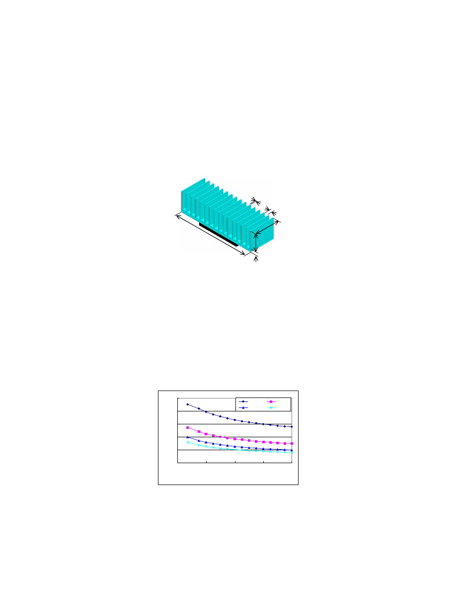
Consider the type of heat-sink shown in Fig.17, which can be directly adopted for use in wash-
ing machines and modified for use in applications like air conditioners. Figs. 18 and 19 show
the analysis results for the heat-sink-to-ambient thermal resistance, R
θha
, in designing the
heat-sink. This varies widely with the changes in fin spacing, fin/base-plate length and fin/
base-plate width. An increase in fin thickness decreases the total number of fins and the size
of the heat-sink, resulting in an increase in thermal resistance.
Fig. 17 A heat-sink example
a=Fin thickness (1.4mm), b=Fin spacing (6.0mm), c=Fin height (25mm)
d=Fin length (37mm), e=Base-plate thickness (4.0mm)
f=Base-plate width (112mm), g=Base-plate length (37mm)
Fig. 18 shows the results to see the effect of the base-plate length on thermal resistance. In
the case where a cooling fan is not used, we can see that the increase in the length to 150%,
that is 55.5mm (37mm
×1.5), reduces the resistance to 82% (≅1.85°C/W), and an increase of
200% (37mm
×=74mm) reduces the resistance to 70.8% (≅1.6°C/W). Fig. 19 is the result of the
variation in the fin height and it shows that the increase in the height to 150%
(25mm
×1.5=37.5mm) reduces the resistance to 80% (≅1.8°c/W). The decrease in the height
to 50% (25mm
×0.5=12.5mm) increases the resistance to 135% (≅3.05°C/W). Therefore,
increasing the height is more effective reducing the thermal resistance, as compared with
increasing the length.
Fig. 18 Analysis results as heat-sink fin & plate length variation
f
e
c
d,g
b
a
0.0
0.5
1.0
1.5
2.0
2.5
30
50
70
90
110
Fin&Base plate length, d, g (mm)
Rha (
℃
/W)
N/C
1m/s
3m/s
5m/s

Rev. A, May 2002
13
Fig.19 Analysis results as heat-sink fin height variation
V. Conclusion
A novel 3-phase IGBT inverter module, the SPM (Smart Power Module), adopting a new
ceramic-based transfer-molding technology, is introduced. Details of the main design con-
cepts, functional capabilities and practical application issues are described. The SPM is tar-
geted at low power inverter applications covering a power rating range up to 3kW at 220Vac
input, resulting in smaller system size, higher reliability, and a better cost-performance ratio.
With its unique technology, the SPM products will be expanded to cover wider power ranges
and applications providing super compact device size in the very near future
0.0
0.5
1.0
1.5
2.0
2.5
3.0
3.5
4.0
10
15
20
25
30
35
40
Fin height, c (mm)
Rha (
℃
/W
)
N/C
1m/s
3m/s
5m/s

14
Rev. A, May 2002
References
[1] T. Yamada et al. "Next Generation Power Module," Intern. Symposium on Power
Semiconductor Devices & IC's, Davos, Switzerland, 1994
[2] Eric R, Motto, John F. Donlon, H. Iwamoto, "New Power Stage Building Blocks for Small
Motor Dirves," Power Electronics '99 Proceedings, pp.343-349, November, 99
[3] Nobuyuki Matsui, "Sensorless PM Brushless DC Motor Drives," IEEE Transactions on
Industrial Electronics, Vol. IE-43, No. 2, pp. 300-308, 1996, April.
[4] F. Casanellas, "Losses in PWM inverters using IGBT's," Proc. Inst. Elect. Eng.-Elect.
Power Applicant. , vol. 141, no. 5, pp. 235-239, Sept.1994.
[5] K. Berringer, J. Marvin and P. Perruchoud, "Semiconductor Power Losses in AC inverters,"
Conf. Rec. of IEEE IAS'95, pp. 882-888, 1995
[6] Smart power module user's guide, application note AN9018, Fairchild Semiconductor

DISCLAIMER
FAIRCHILD SEMICONDUCTOR RESERVES THE RIGHT TO MAKE CHANGES WITHOUT FURTHER
NOTICE TO ANY PRODUCTS HEREIN TO IMPROVE RELIABILITY, FUNCTION OR DESIGN. FAIRCHILD
DOES NOT ASSUME ANY LIABILITY ARISING OUT OF THE APPLICATION OR USE OF ANY PRODUCT
OR CIRCUIT DESCRIBED HEREIN; NEITHER DOES IT CONVEY ANY LICENSE UNDER ITS PATENT
RIGHTS, NOR THE RIGHTS OF OTHERS.
TRADEMARKS
The following are registered and unregistered trademarks Fairchild Semiconductor owns or is authorized to use and is
not intended to be an exhaustive list of all such trademarks.
LIFE SUPPORT POLICY
FAIRCHILDS PRODUCTS ARE NOT AUTHORIZED FOR USE AS CRITICAL COMPONENTS IN LIFE SUPPORT
DEVICES OR SYSTEMS WITHOUT THE EXPRESS WRITTEN APPROVAL OF FAIRCHILD SEMICONDUCTOR CORPORATION.
As used herein:
1. Life support devices or systems are devices or
systems which, (a) are intended for surgical implant into
the body, or (b) support or sustain life, or (c) whose
failure to perform when properly used in accordance
with instructions for use provided in the labeling, can be
reasonably expected to result in significant injury to the
user.
2. A critical component is any component of a life
support device or system whose failure to perform can
be reasonably expected to cause the failure of the life
support device or system, or to affect its safety or
effectiveness.
PRODUCT STATUS DEFINITIONS
Definition of Terms
Datasheet Identification
Product Status
Definition
Advance Information
Preliminary
No Identification Needed
Obsolete
This datasheet contains the design specifications for
product development. Specifications may change in
any manner without notice.
This datasheet contains preliminary data, and
supplementary data will be published at a later date.
Fairchild Semiconductor reserves the right to make
changes at any time without notice in order to improve
design.
This datasheet contains final specifications. Fairchild
Semiconductor reserves the right to make changes at
any time without notice in order to improve design.
This datasheet contains specifications on a product
that has been discontinued by Fairchild semiconductor.
The datasheet is printed for reference information only.
Formative or
In Design
First Production
Full Production
Not In Production
MICROWIRE
OPTOLOGIC
OPTOPLANAR
PACMAN
POP
Power247
PowerTrench
QFET
QS
QT Optoelectronics
Quiet Series
FAST
FASTr
FRFET
GlobalOptoisolator
GTO
HiSeC
I
2
C
ISOPLANAR
LittleFET
MicroFET
MicroPak
Rev. H5
â
ACEx
Bottomless
CoolFET
CROSSVOLT
DenseTrench
DOME
EcoSPARK
E
2
CMOS
TM
EnSigna
TM
FACT
FACT Quiet Series
SILENT SWITCHER
SMART START
SPM
STAR*POWER
Stealth
SuperSOT-3
SuperSOT-6
SuperSOT-8
SyncFET
TinyLogic
TruTranslation
â
â
â
STAR*POWER is used under license
UHC
UltraFET
VCX
â
Wyszukiwarka
Podobne podstrony:
An Igbt Inverter For Interfacing Small Scale Wind Generators To Single Phase Distributed Power Gener
Microprocessor Control System for PWM IGBT Inverter Feeding Three Phase Induction Motor
Microprocessor Control System for PWM IGBT Inverter Feeding Three Phase Induction Motor(1)
Microprocessor Control System for PWM IGBT Inverter Feeding Three Phase Induction Motor(1)
3 Phase inverter IGBT SEMITOP3 module
Microprocessor Control System for PWM IGBT Inverter Feeding Three Phase Induction Motor
Inverter controller for HVDC systems connected to weak AC sy
Zied H A A modular IGBT converter system for high frequency induction heating applications
Inverter For Domestic Fuel Cell Applications
Design Guide 03 Serviceability Design Considerations for Low Rise Buildings
Adaptive fuzzy control for uninterruptible power supply with three phase PWM inverter
12 Active Video Modules for Launchable Reconnaissance Robots
A Composite Pwm Method Of Three Phase Voltage Source Inverter For High Power Applications
Antisocial Guide To Horror Film The Essential Guide For Low Bud (2)
Adaptive fuzzy control for uninterruptible power supply with three phase PWM inverter
On The Specification Of Moving Coil Drivers For Low Frequency Horn Loaded Loudspeakers (W Marshall L
“Metasplizing” Convert an existing exploit to MSF Module
S A Gorden Eyes of an Eagle a Novel of Gravity Controlled v5
więcej podobnych podstron