Philips Semiconductors Linear Products
Product specification
NE/SA/SE4558
Dual general-purpose operational amplifier
65
August 31, 1994
853-0840 13721
DESCRIPTION
The 4558 is a dual operational amplifier that is internally
compensated. Excellent channel separation allows the use of a dual
device in a single amp application, providing the highest packaging
density. The NE/SA/SE4558 is a pin-for-pin replacement for the
RC/RM/RV4558.
FEATURES
•
2MHz unity gain bandwidth guaranteed
•
Supply voltage
±
22V for SE4558 and
±
18V for NE4558
•
Short-circuit protection
•
No frequency compensation required
•
No latch-up
•
Large common-mode and differential voltage ranges
•
Low power consumption
PIN CONFIGURATIONS
D and N Packages
1
2
3
4
5
6
7
8
– +
+ –
A
B
V+
BOUT
AOUT
AIN–
AIN+
V–
BIN–
BIN+
ORDERING INFORMATION
DESCRIPTION
TEMPERATURE RANGE
ORDER CODE
DWG #
8-Pin Plastic Small Outline (SO) Package
0 to +70
°
C
NE4558D
0174C
8-Pin Plastic Dual In-Line Package (DIP)
0 to +70
°
C
NE4558N
0404B
8-Pin Plastic Dual In-Line Package (DIP)
-40 to +85
°
C
SA4558N
0404B
8-Pin Plastic Dual In-Line Package (DIP)
-40 to +85
°
C
SA4558D
0404B
8-Pin Plastic Dual In-Line Package (DIP)
-55 to +125
°
C
SE4558N
0404B
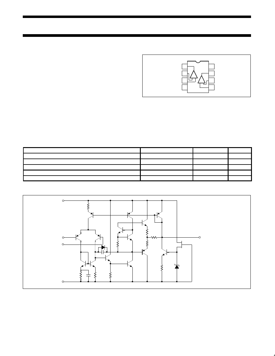
EQUIVALENT SCHEMATIC
8
v+
2(6)
–
INPUTS
3(5)
+
4 V–
OUYPUT 1(7)
Philips Semiconductors Linear Products
Product specification
NE/SA/SE4558
Dual general-purpose operational amplifier
August 31, 1994
66
ABSOLUTE MAXIMUM RATINGS
SYMBOL
PARAMETER
RATING
UNIT
V
CC
Supply voltage
SE4558
±
22
V
NE4558, SA4558
±
18
V
P
D MAX
Maximum power dissipation,
T
A
=25
°
C (Still air)
1
N package
1160
mW
D package
780
mW
Differential input voltage
±
30
V
V
IN
Input voltage
2
±
15
V
T
STG
Storage temperature range
-65 to +150
°
C
T
A
Operating ambient temperature range
SE4558
-55 to +125
°
C
SA4558
-40 to +85
°
C
NE4558
0 to +70
°
C
T
SOLD
Lead soldering temperature (10sec max)
300
°
C
Output short-circuit duration
3
Indefinite
NOTES:
1. Derate above 25
°
C at the following rates:
N package at 9.3mW/
°
C
D package at 6.2mW/
°
C
2. For supply voltages less than
±
15V, the absolute maximum input voltage is equal to the supply voltage.
3. Short-circuit may be to ground on one amp only. Rating applies to +125
°
C case temperature or +75
°
C ambient temperature for NE4558 and
to +85
°
C ambient temperature for SA4558.
DC ELECTRICAL CHARACTERISTICS
V
CC
=
+
15V, TA= 25
°
C unless otherwise specified.
SYMBOL
PARAMETER
TEST CONDITIONS
SE4558
SA/NE4558
UNIT
SYMBOL
PARAMETER
TEST CONDITIONS
Min
Typ
Max
Min
Typ
Max
UNIT
V
OS
Input offset voltage
R
S
≤
10k
Ω
1.0
5.0
2.0
6.0
mV
∆
V
OS
/
∆
T
Over temp.
4
4
µ
V/
°
C
I
OS
Input offset current
50
200
30
200
nA
∆
I
OS
/
∆
T
Over temp.
20
20
pA/
°
C
I
BIAS
Input bias current
40
500
200
500
nA
∆
I
B
/
∆
T
Over temp.
40
40
pA/
°
C
R
IN
Input resistance
0.3
1.0
0.3
1.0
M
Ω
A
V
Large-signal voltage gain
R
L
≥
2k
Ω
V
OUT
=
±
10V
50,00
0
300,0
00
20,00
0
300,0
00
V/V
Output voltage swing
R
L
≥
10k
Ω
R
L
≥
2k
Ω
±
12
±
10
±
14
±
13
±
12
±
10
±
14
±
13
V
V
V
IN
Input voltage range
±
12
±
13
±
12
±
13
V
CMRR
Common-mode rejection ratio
R
S
≤
10k
Ω
70
100
70
100
dB
PSRR
Power supply rejection ratio
R
S
≤
10k
Ω
10
150
10
150
µ
V/V
I
SC
Short-circuit current
5
25
60
5
25
60
mA
Power consumption (all amplifiers)
R
L
=
∞
120
170
120
170
mW
Philips Semiconductors Linear Products
Product specification
NE/SA/SE4558
Dual general-purpose operational amplifier
August 31, 1994
67
DC ELECTRICAL CHARACTERISTICS
(Continued)
SYMBOL
PARAMETER
TEST CONDITIONS
SE4558
SA/NE4558
UNIT
SYMBOL
PARAMETER
TEST CONDITIONS
Min
Typ
Max
Min
Typ
Max
UNIT
t
R
Transient response (unity gain)
V
IN
=20mV
R
L
=2k
Ω
C
L
≤
100pF
t
R
Rise time
100
100
ns
Overshoot
15.0
15.0
%
SR
Slew rate (unity gain)
R
L
≥
2k
Ω
1.0
1.0
V/
µ
s
Channel separation (gain=100)
f=10kHz
R
S
=1k
Ω
90
90
dB
GBW
Unity gain bandwidth (gain=1)
2.0
3.0
2.0
3.0
MHz
θ
M
Phase margin
45
45
De-
gree
V
NOISE
Input noise voltage
f=1k
Ω
25
25
nV/
√
H
z
NOTE:
The following specifications apply over operating temperature range.
V
OS
Input offset voltage
R
S
≤
10k
Ω
6.0
7.5
mV
I
OS
Input offset current
500
300/500
1
nA
I
BIAS
Input bias current
1500
800/1500
1
nA
A
V
Large-signal voltage gain
R
L
≥
2k
Ω
V
OUT
=
±
10V
25,000
15,000
V/V
Output voltage swing
R
L
≥
2k
Ω
±
10
±
10
V
P
C
Power consumption
T
A
=HIGH
T
A
=LOW
105
125
150
200
115
120
150
200
mW
mW
NOTES:
1. SA4558 only.
Philips Semiconductors Linear Products
Product specification
NE/SA/SE4558
Dual general-purpose operational amplifier
August 31, 1994
68
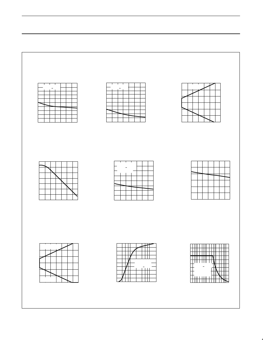
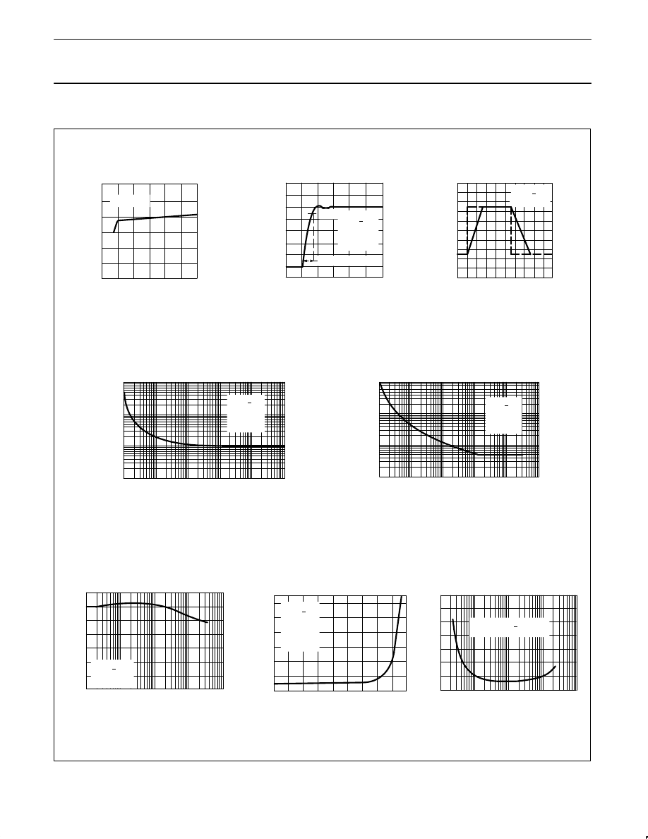
TYPICAL PERFORMANCE CURVES
ÇÇÇÇÇÇÇ
ÇÇÇÇÇÇÇ
ÇÇÇÇÇÇÇ
ÇÇÇÇÇÇÇ
ÇÇÇÇÇÇÇ
ÇÇÇÇÇÇÇ
ÇÇÇÇÇÇÇ
ÇÇÇÇÇÇÇ
ÇÇÇÇÇÇÇ
100
80
60
40
20
0
0
10
20
30
40
50
60 70
TEMPERATURE (
o
C)
INPUT BIAS CURRENT (
A)
µ
VS = + 15V
25
20
15
10
5
0
0
10
20
30
40
50
60 70
TEMPERATURE (
o
C)
INPUT offset current (
A)
µ
TA = 25
o
C
–15
–10
–5
0
5
10
15
4
6
8
10 12
14 16
18
SUPPLY VOLTAGE (V)
COMMON MODE
VOL
T
AGE RANGE (V)
ÇÇÇÇÇÇÇ
ÇÇÇÇÇÇÇ
ÇÇÇÇÇÇÇ
ÇÇÇÇÇÇÇ
ÇÇÇÇÇÇÇ
ÇÇÇÇÇÇÇ
ÇÇÇÇÇÇÇ
ÇÇÇÇÇÇÇ
ÇÇÇÇÇÇÇ
TA = 25
o
C
15
10
5
0
–5
–10
–15
4
6
8
10 12
14 16
18
RL = 2K
Ω
SUPPLY VOLTAGE (V)
OUTPUT SWING (V)
VS = + 15V
800K
600K
400K
200K
0K
0
10
20
30
40
50
60
70
RL = 2K
Ω
VS = + 15V
TEMPERATURE (
o
C)
VOL
T
AGE GAIN
POWER CONSUMPTION (mV)
0
10
20
30
40 50
60
70
TEMPERATURE (
o
C)
140
130
120
110
100
90
80
120
100
80
60
40
20
0
–20
1
10 100 1K 10K 100K1K 10M
FREQUENCY (Hz)
VOL
T
AGE GAIN (dB)
28
26
24
22
20
18
16
14
12
10
8
0.1 0.2
0.5 1.0 2.0
5.0
10
LOAD RESISTANCE (K
Ω
))
PEAK T
O PEAK
OUTPUT SWING (V)
VS = + 15V
TA = 25
o
C
40
36
32
28
24
20
18
12
8
4
0
PEAK T
O PEAK
OUTPUT SWING (V)
100
1K
10K
100K
1M
FREQUENCY (Hz)
VS = + 15V
TA = 25
o
C
RL = 25K
Ω
Input Bias as a
Function of Ambient
Temperature
Input Offset Current as
as a Function of Ambient
Temperature
Common–Mode Range as
a Function of Supply
Voltage
Open–Loop Voltage Gain
as a Function of
Frequency
Open–Loop Gain as a
Function of
Temperature
Power Consumption as
a Function of Ambient
Temperature
Typical Output Voltage
as a Function of
Supply Voltage
Output Voltage Swing
as a Function of
Load Resistance)
Output Voltage Swing
as a Function of
Frequency
VS = + 15V
Philips Semiconductors Linear Products
Product specification
NE/SA/SE4558
Dual general-purpose operational amplifier
August 31, 1994
69
TYPICAL PERFORMANCE CURVES (Continued)
VS = + 15V
TA = 25
o
C
6
5
4
3
2
1
0
0
3
6
9
12
15
18
SUPPLY VOLTAGE (V)
TA = 2
5o
C
QUIESCENT CURRENT (mA)
100
10
1
0.1
1
10
100
1K
FREQUENCY (Hz)
10K
100K
NOISE CURRENT (P
A
Hz)
√
RS = 100K
AV = 60dB
VS = + 15V
T = 25
o
C
NOISE CURRENT (nV Hz)
√
1000
100
10
1
1
10
100
1K
FREQUENCY (Hz)
10K
100K
RS = 50
Ω
AV = 60dB
VS = + 15V
TA = 25
o
C
90%
10% RISE TIME
28
24
20
16
12
8
4
0
OUTPUT (mV)
0
.25
.50
.75
1.0
1.25
TIME (
µ
S)
RS = 2K
Ω
CL = 100pF
VS = + 15V
TA = 25
o
C
10
8
6
4
2
0
–2
–4
–6
–8
–10
0
5 10
20
TIME (
µ
S)
OUTPUT VOL
T
AGE
30
40
140
120
100
80
60
40
20
0
10
100
1K
10K
FREQUENCY (Hz)
100k
CHANNEL
SEP
ARA
TION (dB)
VS = +
15V
TA = 25
o
C
6
5
4
3
2
1
0
1
2
3
4
5
6
7
8
9
10
VO OUTPUT VOLTAGE (VRMS)
T
OT
AL
HARMONIC DISTROTION
ON (2) 1kHz (%)
VS = +
15V
RL = 2K
Ω
AV = 40dB
= 1kHz
RS = 1K
Ω
V10S = +30V
RIAA COMPENSATION
7
6
5
4
3
2
1
0
0
100
1K
10K
100K
FREQUENCY (Hz)
T
OT
AL
HARMONIC DIST
ORA
TION (%)
Quiescent Current as a
Function of
Supply Voltage
Transient Response
Voltage–Follower
Large–Signal Pulse
Response
Input Noise Voltage as a Function
of Frequency
Input Noise Current as a Function
of Frequency
Channel Separation
Total Harmonic Distortion vs
Output Voltage
Distortion vs Frequency
V
O
= 1V
RMS
Wyszukiwarka
Podobne podstrony:
NE(SA,SE)556
Ne zajebavaj se sa životinjama
NE SA SE555 C 2
Obiat Komorowski i SE są w błędzie
to se ne wrati 2
to se ne wrati
to se ne wrati
to se ne wrati
to se ne wrati
więcej podobnych podstron