
MOTOROLA
SEMICONDUCTOR TECHNICAL INFORMATION
MC9S12H256MSE2 Rev 2
January 23, 2003
When contacting a Motorola representative for assistance, please have the MCU
device mask set and date code information available.
Specifications and information herein are subject to change without notice.
© Motorola, Inc., 2003
MSE Published Date: January 23, 2003
Mask Set Errata 2
MC9S12H256 Microcontroller Unit
INTRODUCTION
This errata provides information applicable to the following MCU mask set devices:
•
1K78X mask of the MC9S12H256 and MC9S12H128
MCU DEVICE MASK SET IDENTIFICATION
The mask set is identified by a four-character code consisting of a letter, two
numerical digits, and a letter, for example F74B. Slight variations to the mask set
identification code may result in an optional numerical digit preceding the standard
four-character code, for example 0F74B.
MCU DEVICE DATE CODES
Device markings indicate the week of manufacture and the mask set used. The
data is coded as four numerical digits where the first two digits indicate the year
and the last two digits indicate the work week. The date code “9115” would indicate
the 15th week of the year 1991.
MCU DEVICE PART NUMBER PREFIXES
Some MCU samples and devices are marked with an SC, PC, ZC or XC prefix. An
SC, PC or ZC prefix denotes special/custom device. An XC prefix denotes device
is tested but is not fully characterized or qualified over the full range of normal
manufacturing process variations. After full characterization and qualification,
devices will be marked with the MC prefix.
ERRATA SYSTEM TRACKING NUMBERS
MUCTS00xxx is the tracking number for device errata. It can be used with the mask
set and date code to identify a specific errata to a Motorola representative.

2
MC9S12H256 Rev 2
January 23, 2003
ERRATA SUMMARY
Errata
Number
Module
affected
Brief description
Workaround
available?
First
Issued
MUCts00425
ATD
ATD current consumption in low power modes
Yes
Rev 1
MUCts00436
BDM
BDM loses sync when using PLL at high frequencies
Yes
Rev 1
MUCts00446
SPI
SPI locks if disabled during message transmission
Yes
Rev 1
MUCts00459
OSC
Clock Monitor Frequency lower than specified
N/A
Rev 1
MUCts00462
MC
Erroneous Waveforms in Dual Full H-Bridge Mode
Yes
Rev 1
MUCts00465
PWM
PWM channel early start after leaving emergency shutdown mode
No
Rev 1
MUCts00468
S12_BKP
Breakpoint Module: potential extraneous date match
Yes
Rev 1
MUCts00487
SPI
SPI can receive incorrect data in slave mode
Yes
Rev 1
MUCts00489
SPI
SPIF-flag is set wrongly in slave mode after SPI re-enabling
Yes
Rev 1
MUCts00491
SPI
SPI locks if re-enabled as master
Yes
Rev 1
MUCts00505
MEBI
Non-multiplexed Address on PK change before end of cycle
Yes
Rev 1
MUCts00510
SCI
SCI interrupt asserts only if an odd number of interrupts active
Yes
Rev 1
MUCts00537
SPI
SPIF flag is set wrongly in slave mode
Yes
Rev 1
MUCts00543
MSCAN
MSCAN extended ID rejected if stuff bit between ID16 and ID15
Yes
Rev 1
MUCts00559
SPI
SPIF flag is set wrongly -> SPI locks in master mode
Yes
Rev 1
MUCts00564
MEBI
Missing external ECLK during reset vector fetch
No
Rev 1
MUCts00573
SPI
SPIDR is writeable though the SPTEF flag is cleared
Yes
Rev 1
MUCts00576
FLASH
Erase Verify impact on subsequent Erase operations
Yes
Rev 1
MUCts00590
MSCAN
Glitch filter exceeds spec limits
No
Rev 1
MUCts00618
KWU
Key wake-up: Glitch filter exceeds upper 10
µ
s limit
No
Rev 1
MUCts00641
EEPROM
Program & Erase of EEPROM blocked in Normal Single Chip Mode
when secure
Yes
Rev 1
MUCts00642
FLASH
Program & Erase of Flash blocked in Normal Single Chip Mode
when secure
Yes
Rev 1
MUCts00704
SPI
SPTEF flag set wrongly
Yes
Rev 1
MUCts00737
ATD
Flags in ATDSTAT0 do not clear by writing “1”, ETORF sets
wrongly
Yes
Rev 1
MUCts00746
SPI
SPI in mode fault state, but MISO output buffer not disabled
No
Rev 1
MUCts00782
PIM
Port L GPIO/LCD select error
Yes
Rev 1
MUCts00795
SPI
MISO not kept after sixteenth SCK edge
Yes
Rev 1
MUCts00802
ATD
Write to ATDCTL5 may not clear SCF, CCF and ASCIF flags
Yes
Rev 1

MC9S12H256 Rev 2
3
January 23, 2003
ATD CURRENT CONSUMPTION IN LOW POWER MODES
MUCTS00425
If ATD module is enabled when the CPU encounters the STOP instruction or the
CPU encounters the WAI instruction with the ATD Stop in Wait bit set, ATD current
consumption may be out of specification.
Work-
around
The ATD module should be disabled prior to entering stop mode.
BDM LOSES SYNC WHEN USING PLL AT HIGH FREQUENCIES
MUCTS00436
When using the BDM constant clock source, i.e. CLKSW=0, with the PLL engaged,
pllsel=1, and the PLL multiplier greater than or equal to 2, the BDM can lose
communication with the host system.
Work-
around
Do not use the BDM constant clock source with the PLL engaged and a multiplier
greater than or equal to 2. Set CLKSW=1 before engaging the PLL.
SPI LOCKS IF DISABLED DURING MESSAGE TRANSMISSION MUCTS00446
In master mode during a transmission SPI locks if SPE bit is cleared. After
re-enabling, writing to SPIDR does not result in message transmission.
Work-
around
Disable the SPI module only if transmission queue is empty (SPTEF=1) and
transfer is complete (SPIF=1).
CLOCK MONITOR FREQUENCY LOWER THAN SPECIFIED
MUCTS00459
The clock monitor failure assert frequency is f_CMFA=(max:100khz, typ:50kHz,
min:25kHz) and not as the specified f_CMFA=(max:200khz, typ:100kHz,
min:50kHz).
Work-
around
N/A

4
MC9S12H256 Rev 2
January 23, 2003
ERRONEOUS WAVEFORMS IN DUAL FULL H-BRIDGE MODE MUCTS00462
In dual full H-bridge mode, when an even duty cycle register is updated before the
odd duty cycle register is written and a PWM counter overflow occurs:
1. An erroneous waveform may be generated on the even channel when
changing the Sign bit in right, left and center aligned mode.
2. An erroneous waveform may be generated on the even channel when
changing the duty cycle value “from” duty cycle 100% or changing the duty
cycle value “to” duty cycle 100% in right aligned mode.
3. An erroneous waveform may be generated on the even channel when
changing the duty cycle value “from” duty cycle 0% “from” duty cycle 100%
“to” duty cycle 0% “to” duty cycle 100% in center and left aligned mode.
Work-
around
a. Update even and odd duty cycle registers just after a counter overflow has
been detected by using the MCTOIF flag.
b. Restrict PWM operation to right aligned mode not using 100% duty cycle.
PWM CHANNEL EARLY START AFTER LEAVING EMERGENCY SHUTDOWN
MODE
MUCTS00465
When recovering from the emergency shutdown mode by disasserting the active
level on the PWM emergency shutdown input pin and subsequently asserting the
PWMRSTRT bit, the enabled PWM channels do not hold the shutdown output level
(PWMLVL) until the corresponding counter passes zero. This may result in a pulse
of undefined length on enabled PWM channels.
Work-
around
None

MC9S12H256 Rev 2
5
January 23, 2003
BREAKPOINT MODULE: POTENTIAL EXTRANEOUS DATA MATCH
MUCTS00468
When using the breakpoint in full mode with the read/write match function disabled,
there is a chance of a false match. Internally there is a separate read data bus and
write data bus. When in full mode with the read/write match function is disabled,
both buses are always compared to the contents of data match register. The circuit
should only match the active bus on any particular bus cycle. The false match can
occur if the address matches on a read cycle and matching data is on the write data
bus or the address matches on a write cycle and the matching data is on the read
data bus.
Work-
around
When using full mode, always enable the read/write match and select the
appropriate state of read/write. This will avoid false matches.
SPI CAN RECEIVE INCORRECT DATA IN SLAVE MODE
MUCTS00487
An SPI configured for slave mode operation can receive incorrect data. If there are
clock edges on SCK while SPE=0, and then SPE is set to one, the received data
will be incorrect. In CPHA=1 mode the SPI will continue to receive incorrect data
as long as SPE=1.
Work-
around
Depending on the current mode on SPI, the following bits have to be configured
while disabling the SPI:
Set CPHA=1 and make sure that the CPOL-bit is clear every time the SPI is
disabled from slave mode.
Clear CPHA and make sure that CPOL is clear as well every time the SPI is
disabled from master mode.
SPIF-FLAG IS SET WRONGLY IN SLAVE MODE AFTER SPI RE-ENABLING
MUCTS00489
The SPIF-flag is set wrongly under the following conditions:
- receiving a byte with the SPI while configured as slave, CPHA=1 and CPOL=1
- clearing SPIF in SPISR normally (read SPISR followed by a read of SPIDR)
- disabling the SPI through clearing SPICR1
- re-enabling the SPI (with CPHA=1 and CPOL=1)
Three bus cycles after this sequence SPIF in SPISR is set, which is not correct.

6
MC9S12H256 Rev 2
January 23, 2003
Work-
around
A sequence to clear the wrong SPIF is:
If no other IRQs enabled:
•
Insert a short delay (min. 3 bus cycles) after re-enabling the SPI and clear
the SPIF by reading the SPISR followed by SPIDR after re-enabling the SPI.
If other IRQs enabled (excluding X-IRQ):
•
before re-enabling the SPI, disable all IRQs through a set of bit CCR[4] (IRQ
mask) using the instruction SEI
•
re-enable SPI, insert a short delay (min. 3 bus cycles) after SPI re-enabling
•
clear SPIF by a read access to the SPISR followed by SPIDR.
•
re-enable all IRQs through clearing bit CCR[4] using the instruction CLI
In the case where a hardware interrupt is used, it is possible to lose an SPI IRQ.
SPI LOCKS IF RE-ENABLED AS MASTER
MUCTS00491
The SPI locks if it is disabled in master mode with CPHA=1 in SPICR1 and
re-enabled in master mode with CPHA=1.
Work-
around
Make sure that CHPA is not set when SPI is disabled after a transmission in master
mode.
NON-MULTIPLEXED ADDRESSES ON PK CHANGE BEFORE END OF CYCLE
MUCTS00505
In expanded modes with the EMK emulate port k bit set and the EXSTR[1:0]
external access stretch bits 1 & 0 set to 01, 10 or 11 the non-multiplexed addresses
on PK[5:0] change during E clock high phase at t4.
Work-
around
If the external access is stretched (EXSTR[1:0] set to 01, 10 or 11) off chip address
latches should be used to register the non-multiplexed addresses on PK[5:0].

MC9S12H256 Rev 2
7
January 23, 2003
SCI INTERRUPT ASSERTS ONLY IF AN ODD NUMBER OF INTERRUPTS
ACTIVE
MUCTS00510
The interrupt of the SCI is only asserted if an odd number of interrupts is active (i.e.
flags set and enabled). Example: If an Transmit data register empty and an receive
ready interrupt are active at the same time the interrupt request to the CPU is not
asserted. This can lead to missing interrupts or spurious interrupts i.e. the request
gets deasserted before the CPU fetches the interrupt vector. Those spurious
interrupts will execute on the SWI vector. The interrupt flag setting is always
correct.
Work-
around
There is no general workaround. Some typical cases will be described. The
problem is reduced by fast interrupt response times and slow Baud rates.
1. Single wire interfaces as used in the automotive industry Since the transmit
and receive process are linked to each other a mix of interrupt handling and
polling is possible. Here several scenarios are possible to come to a stable
operation but each might require a rewriting of the lower level drivers. The
easiest one is to use only receive interrupt and fill the first two bytes of a
message into the transmit queue by polling. With each byte received the
transmit data buffer is empty and a new byte can be queued.
2. Full duplex operation If the SCI interrupt is not asserted while e.g. a transmit
or receive interrupt are pending the received byte will cause an overflow error
(3rd interrupt) and this will then assert the interrupt. A software can detect the
overrun error and request a re-transmission of the last message frame. One
byte is lost here. Polling flag bits at a frequency of one byte time. (E.g. 1ms
for 9600 bd) Toggling one of the enable flags at the frequency of one byte.
SPIF FLAG IS SET WRONGLY IN SLAVE MODE
MUCTS00537
If an SPI is enabled in slave mode with the CPHA bit set, all other bits in their reset
state, and SS/SCK pins driven low then clearing the CPHA bit will cause the SPIF
bit to be set three Bus Clock cycles after the CPHA bit is cleared.
Work-
around
Change of CPHA bit should only occur while SPI is disabled (SPE bit cleared).

8
MC9S12H256 Rev 2
January 23, 2003
MSCAN EXTENDED ID REJECTED IF STUFF BIT BETWEEN ID16 AND ID15
MUCTS00543
For 32-bit and 16-bit identifier acceptance modes, an extended ID CAN frame with
a stuff bit between ID16 and ID15 can be erroneously rejected, depending on
IDAR0, IDAR1, and IDMR1.
Extended IDs (ID28-ID0) which generate a stuff bit between ID16 and ID15:
where x = 0 or 1 (don't care)
*
= pattern for ID28 to ID18 (see following).
Affected extended IDs (ID28 - ID18) patterns:
a)
xxxxxxxxx01
exceptions:
01111100001
xxxx1000001
except
11111000001
b)
xxxxx100000
exception:
01111100000
c)
xxxx0111111
d)
x0111110000
e)
10000000000
f)
11111111111
g)
10000011111
When an affected ID is received, an incorrect value is compared to the 2nd byte of
the filter (IDAR1 and IDAR5, plus IDAR3 and IDAR7 in 16-bit mode). This incorrect
value is the shift register contents before ID15 is shifted in (i.e. right shifted by 1).
Work-
around
If the problematic IDs cannot be avoided, the workaround is to mask certain bits
with IDMR1 (and IDMR5, plus IDMR3 and IDMR7 in 16-bit mode).
Example 1: to receive the message IDs
xxxx xxxx x011 111x xxxx xxxx xxxx xxxx
IDMR1 etc. must be 111x xxx1, i.e. ID20,19,18,15 must be masked.
Example 2: to receive the message IDs
xxxx 0111 1111 111x xxxx xxxx xxxx xxxx
IDMR1 etc. must be 1xxx xxx1, i.e. ID20 and ID15 must be masked.
In general, using IDMR1 etc. 1111 xxx1, i.e. masking ID20,19,18,SRR,15, hides
the problem.
IDAR0
IDAR1
IDAR2
IDAR3
********
***1111x
xxxxxxxx
xxxxxxxx

MC9S12H256 Rev 2
9
January 23, 2003
SPIF FLAG IS SET WRONGLY – SPI LOCKS IN MASTER MODE
MUCTS00559
The SPIF flag is set wrongly after the following sequence:
1. SPI receives a byte in slave mode
SPIF flag is cleared normally (read SPISR, read SPIDR)
2. SPI is disabled through the following sequence
(given by workaround for MUCts00487 and MUCts00491)
SPICR1 is set to 0x04h
3. SPI is re-enabled as master through the following sequence
(given by workaround for MUCts00487 and MUCts00491)
SPICR1 is set to 0x08h, SPICR1 is set to 0x54h
Three bus cycles after SPICR1 was set to 0x08h, the SPIF flag is set wrongly
and also the master locks
Work-
around
1. SPI receives a byte in slave mode
SPIF flag is cleared normally (read SPISR, read SPIDR)
2. Disable SPI through the following sequence
(given by workaround for MUCts00487 and MUCts00491)
Set SPICR1 to 0x04h
3. Re-enable SPI as master through the following sequence
(given by workaround for MUCts00487 and MUCts00491)
Set SPICR1 to 0x0Ch (actual workaround for MUCts00559)
Set SPICR1 to 0x08h
Set SPICR1 to 0x54h
MISSING EXTERNAL ECLK DURING RESET VECTOR FETCH MUCTS00564
The reset conditions of the ECLK control logic in the MEBI inhibit the generation of
1 ECLK pulse during the reset vector fetch. This can prevent the external logic from
latching the reset vector address.
Work-
around
None

10
MC9S12H256 Rev 2
January 23, 2003
SPIDR IS WRITEABLE THOUGH THE SPTEF FLAG IS CLEARED
MUCTS00573
Data can be placed into the SPI Data Register (SPIDR) though the SPTEF flag is
cleared. The SPTEF flag indicates, if the transmit buffer is empty (SPTEF=1) or full
(SPTEF=0). Data can be placed into the SPI Data Register by reading SPISR with
SPTEF=1 followed by a write to the SPI Data Register. If SPTEF=0, a write to the
SPI Data Register should be ignored, according to the SPI specification. This is not
true for the current implementation, where data can be placed into the SPI Data
Register though SPTEF=0.
Work-
around
Do not write to the SPI Data Register until you have read SPISR with SPTEF=1.
ERASE VERIFY IMPACT ON SUBSEQUENT ERASE OPERATIONS
MUCTS00576
If the Erase Verify ($05) command is issued on an array that is not erased as
indicated by the FSTAT/ESTAT BLANK bit not being set upon command
completion, the execution of the Sector Erase ($40) or Mass Erase ($41) command
will not properly erase the intended region. The Program ($20) command will
execute properly.
Work-
around
If the Erase Verify ($05) command is issued on an array that is not erased,
subsequent Sector Erase ($40) or Mass Erase ($41) commands must be issued
twice before the intended region is properly erased.
GLITCH FILTER EXCEEDS SPEC LIMITS
MUCTS00590
The specified MSCAN wake-up glitch filter pulse limits can be exceeded. At low
temp/high VDD the module may wake up from sleep mode on glitches <2
µ
s while
for pulses >5
µ
s it may not wake up from sleep mode at high temp/low VDD. The
device operates at relaxed limits:
MSCAN Wake-up dominant pulse filtered: max. 1
µ
s
MSCAN Wake-up dominant pulse pass: min. 7
µ
s
Work-
around
None

MC9S12H256 Rev 2
11
January 23, 2003
KEY WAKE-UP: GLITCH FILTER EXCEEDS UPPER 10
µ
S LIMIT MUCTS00618
The specified maximum limit of the key wake-up glitch filter pulse can be exceeded
in corner cases. At high temp/low VDD the STOP mode may not be left on pulses
>=10
µ
s. The device operates at a relaxed limit of 11
µ
s.
Work-
around
None
PROGRAM & ERASE OF EEPROM BLOCKED IN NORMAL SINGLE CHIP
MODE WHEN SECURE
MUCTS00641
In normal single chip mode, when security is enabled, it is not possible to launch
the Program ($20), Sector-Erase ($40), Sector-Modify ($60) and Erase-Verify
($05) commands in the EEPROM. The Mass-Erase ($41) command can be
launched.
Work-
around
To enable the Program ($20), Sector-Erase ($40) and Erase-Verify ($05)
commands in the flash, security must be disabled via the backdoor key sequence.
See Flash User Guide for details of the backdoor key operation.
PROGRAM & ERASE OF FLASH BLOCKED IN NORMAL SINGLE CHIP MODE
WHEN SECURE
MUCTS00642
In normal single chip mode, when security is enabled, it is not possible to launch
the Program ($20), Sector-Erase ($40) and Erase- Verify ($05) commands in the
Flash. The Mass-Erase ($41) command can be launched.
Work-
around
To enable the Program ($20), Sector-Erase ($40) and Erase-Verify ($05)
commands in the flash, security must be disabled via the backdoor key sequence.
See Flash User Guide for details of the backdoor key operation.
12
MC9S12H256 Rev 2
January 23, 2003
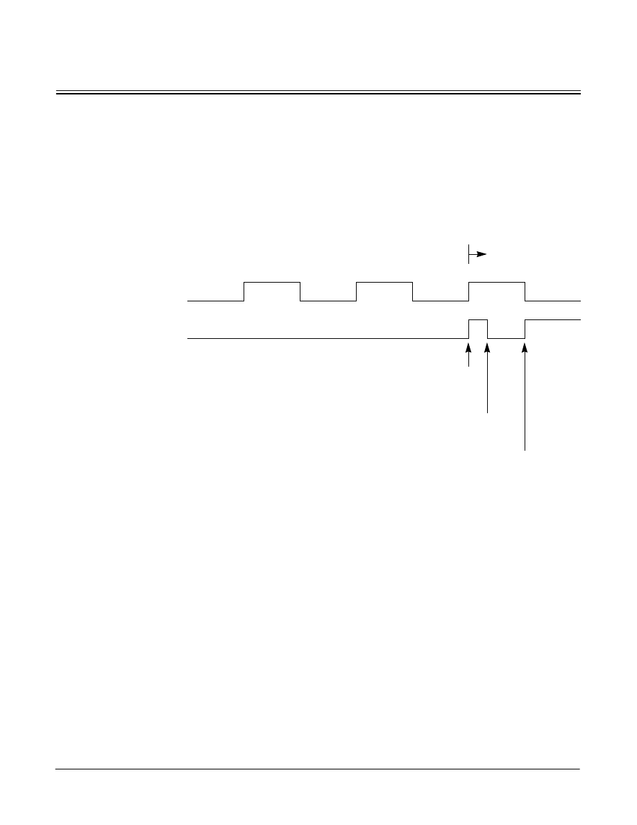
SPTEF FLAG SET WRONGLY
MUCTS00704
When the SPI is enabled in master mode, with the CPHA bit set, back to back
transmissions are possible.
When a transmission completes and a further byte is available in the SPI Data
Register, the second transmission begins directly after the “minimum trailing time”.
The problem occurs when, after the SPTEF flag has been set, a further byte is
written into the SPI Data Register during the “1st pulse” of a subsequent
transmission .
Then the SPTEF flag is set at the falling SCK edge of the “1st pulse” and data is
transferred from the SPI Data Register to the transmit shift register. The result is
that the transmission is corrupted and data is lost.
Work-
around
After the SPTEF flag has been set, a delay of 1/2 SCK period has to be added
before storing data into the SPI Data Register.
SCK
7th pulse
8th pulse
1st pulse
SPTEF
next transmission
End of transmission
SPTEF flag is being set
Write to SPIDR
during “1st pulse”
SPTEF flag set again (WRONG)

MC9S12H256 Rev 2
13
January 23, 2003
ATD: FLAGS IN ATDSTAT0 DO NOT CLEAR BY WRITING ‘1’, ETORF SETS
WRONGLY
MUCTS00737
For the flags SCF, ETORF and FIFOR in ATDSTAT0 it is specified that: Write ‘1’
to the respective flag clears it. This does not work. Writing ‘1’ to the respective flag
has no effect. The ETORF flag is also set by a non active edge, e.g. falling edge
trigger (ETRILE=0, ETRIGP=0). ETORF is set on both falling edges and rising
edges while conversion is in progress.
Work-
around
SCF
1. Use the alternative flag clearing mechanisms:
a. Write to ATDCTL5 (a new conversion sequence is started)
b. If AFFC=1 a result register is read
ETORF
1. Use the alternative flag clearing mechanisms:
a. Write to ATDCTL2, ATDCTL3 or ATDCTL4 (a conversion sequence is
aborted)
b. Write to ATDCTL5 (a new conversion sequence is started)
2. Avoid external trigger edges during conversion process by using short
pulses
3. Ignore ETROF flag
FIFOR
1. Use the alternative flag clearing mechanism:
a. Start a new conversion sequence (write to ATDCTL5 or external trigger)

14
MC9S12H256 Rev 2
January 23, 2003
SPI: SPI IN MODE FAULT STATE, BUT MISO OUTPUT BUFFER NOT
DISABLED
MUCTS00746
When the SPI is in Mode Fault state (MODF flag set), according to the
specification, all SPI output buffers (SS, SCK, MOSI, MISO) should be disabled.
However, the MISO output buffer is not disabled.
Work-
around
None
PORT L GPIO/LCD SELECT ERROR
MUCTS00782
GPIO or LCD functionality is not controlled properly on Port L. FPEN31 controls
PL3 instead of PL7, FPEN30 controls PL2 instead of PL6, FPEN29 controls PL1
instead of PL5, FPEN28 controls PL0 instead of PL4, FPEN19 controls PL7
instead of PL3, FPEN18 controls PL6 instead of PL2, FPEN17 controls PL5
instead of PL1, FPEN16 controls PL4 instead of PL0, while the LCD outputs are
routed correctly. If, for example, FPEN31 is set while FPEN19 is cleared, PL7 can
be used as GPIO via the Port L data and data direction registers, while at the same
time the LCD module tries to drive PL7. Erroneous output function can occur in this
case on PL7 as well as on other enabled LCD pins.
Work-
around
To resolve conflicts, customers should use the same type of pin purpose on the pin
pairs PL7 and PL3, PL6 and PL2, PL5 and PL1 as well as PL4 and PL0.
If an odd number of LCD pins is required by the application, it is recommended to
use Port L in an even fashion and use an odd number on any other port with LCD
shared.
On 112 pin parts, if any pin of PL3 .. PL0 are used for LCD the corresponding
FPEN31 .. FPEN28 should be set to clear PL3 .. PL0 for LCD usage.
SPI: MISO NOT KEPT AFTER SIXTEENTH SCK EDGE
MUCTS00795
In SPI slave mode with CPHA set, MISO can change falsely after a transmission,
two to three bus clock cycles after the sixteenth SCK edge. This can lead to a hold
time violation on the SPI master side.
Work-
around
There are two possible workarounds for this problem:
1. Decrease the bus clock of the slave SPI to satisfy the "Masters MISO Hold
Time".
Tbus(Slave) >= 0.5 * "Masters MISO Hold Time"

MC9S12H256
Motorola reserves the right to make changes without further notice to any products herein. Motorola makes no warranty, representation or guarantee regarding the suitability of its
products for any particular purpose, nor does Motorola assume any liability arising out of the application or use of any product or circuit, and specifically disclaims any and all liability,
including without limitation consequential or incidental damages. "Typical" parameters which may be provided in Motorola data sheets and/or specifications can and do vary in different
applications and actual performance may vary over time. All operating parameters, including "Typicals" must be validated for each customer application by customer's technical experts.
Motorola does not convey any license under its patent rights nor the rights of others. Motorola products are not designed, intended, or authorized for use as components in systems
intended for surgical implant into the body, or other applications intended to support or sustain life, or for any other application in which the failure of the Motorola product could create a
situation where personal injury or death may occur. Should Buyer purchase or use Motorola products for any such unintended or unauthorized application, Buyer shall indemnify and hold
Motorola and its officers, employees, subsidiaries, affiliates, and distributors harmless against all claims, costs, damages, and expenses, and reasonable attorney fees arising out of,
directly or indirectly, any claim of personal injury or death associated with such unintended or unauthorized use, even if such claim alleges that Motorola was negligent regarding the
design or manufacture of the part. Motorola and
are registered trademarks of Motorola, Inc. Motorola, Inc. is an Equal Opportunity/Affirmative Action Employer.
Additional mask set errata can be found on the World Wide Web at http://www.mcu.motsps.com/documentation/index.html
January 23, 2003
2. Software workaround:
The slave has to transmit a dummy byte after each data byte, which must
fulfill the following requirements:
•
The dummy bytes first bit to be transmitted (depending on LSBFE bit) must
be equal to the last bit of the data byte transmitted before.
The dummy byte has to be stored into SPIDR during the transmission of the
corresponding data byte.
=> MISO does not change after the data byte.
•
The Master has to receive two bytes, the data byte and the dummy byte.
=> Master receives the data byte correctly and has to skip the dummy
byte.
WRITE TO ATDCTL5 MAY NOT CLEAR SCF, CCF AND ASCIF FLAGS
MUCTS00802
If a write to ATDCTL5 happens at exactly the bus cycle where an ongoing
conversion sequence ends, the SCF, CCF and (if ASCIE=1) ASCIF flags remain
set and are NOT cleared by a write to ATDCTL5.
Work-
around
1. Ensure device is protected from interrupts (temporarily disable interrupts
with the I mask bit).
2. Write to ATDCTL5 twice.
Document Outline
- introduction
- MCU Device Mask Set Identification
- MCU Device Date Codes
- MCU Device Part Number Prefixes
- Errata System Tracking Numbers
- ERRATA SUMMARY
- ATD current consumption in low power modes MUCTS00425
- BDM loses sync when using PLL at high frequencies MUCts00436
- SPI locks if disabled during message transmission MUCts00446
- Clock Monitor Frequency lower than specified MUCts00459
- Erroneous Waveforms in Dual Full H-Bridge Mode MUCts00462
- PWM channel early start after leaving emergency shutdown mode MUCts00465
- Breakpoint Module: potential extraneous datA match MUCts00468
- SPI can receive incorrect data in slave mode MUCts00487
- SPIF-flag is set wrongly in slave mode after SPI re-enabling MUCts00489
- SPI locks if re-enabled as master MUCts00491
- Non-Multiplexed Addresses on PK change before end of cycle MUCts00505
- SCI interrupt asserts only if an odd number of interrupts active MUCts00510
- SPIF flag is set wrongly in slave mode MUCts00537
- MSCAN extended ID rejected if stuff bit between ID16 and ID15 MUCts00543
- SPIF flag is set wrongly – SPI locks in master mode MUCts00559
- Missing external ECLK during reset vector fetch MUCts00564
- SPIDR is writeable though the SPTEF flag is cleared MUCts00573
- Erase Verify impact on subsequent Erase operations MUCts00576
- Glitch filter exceeds spec limits MUCts00590
- Key wake-up: Glitch filter exceeds upper 10ms limit MUCts00618
- Program & Erase of EEPROM blocked in Normal Single Chip Mode when secure MUCts00641
- Program & Erase of Flash blocked in Normal Single Chip Mode when secure MUCts00642
- SPTEF flag set wrongly MUCts00704
- ATD: Flags in ATDSTAT0 do not clear by writing ‘1’, ETORF sets wrongly MUCts00737
- SPI: SPI in Mode Fault state, but MISO output buffer not disabled MUCts00746
- Port L GPIO/LCD select error MUCts00782
- SPI: MISO not kept after sixteenth SCK edge MUCts00795
- Write to ATDCTL5 may not clear SCF, CCF and ASCIF flags MUCts00802
Wyszukiwarka
Podobne podstrony:
MC9S12A128 Mask Set Errata
MC9S12DT128 Mask Set Errata 1
MC9S12D64 Mask Set Errata 2
MC9S12D64 Mask Set Errata 3
MC9S12DT128 Mask Set Errata 2
MC68HC912B32 Mask Set Errata 1
MC68HC912B32 Mask Set Errata 1
MC68HC912BC32 Mask Set Errata 2
MC68HC12BE32 Mask Set Errata 4
MC68HC12D60 Mask Set Errata 1
MC68HC812A4 Mask Set Errata 1
PC9S12D64 PC9S12DJ64 Mask Set Errata 1
MC68HC912DG128A Mask Set Errata 1
MC68HC912D60C Mask Set Errata 1
MC68HC912BC32 Mask Set Errata 1
MC68HC12BE32 Mask Set Errata 3
PC9S12H256 Mask Set Errata 1
MC68HC912D60A Mask Set Errata 1
więcej podobnych podstron