1
Motorola Small–Signal Transistors, FETs and Diodes Device Data
PNP Silicon
MAXIMUM RATINGS
Rating
Symbol
BC307, B, C
BC308C
Unit
Collector – Emitter Voltage
VCEO
–45
–25
Vdc
Collector – Base Voltage
VCBO
–50
–30
Vdc
Emitter – Base Voltage
VEBO
–5.0
Vdc
Collector Current — Continuous
IC
–100
mAdc
Total Device Dissipation @ TA = 25
°
C
Derate above 25
°
C
PD
350
2.8
mW
mW/
°
C
Total Device Dissipation @ TC = 25
°
C
Derate above 25
°
C
PD
1.0
8.0
Watts
mW/
°
C
Operating and Storage Junction
Temperature Range
TJ, Tstg
– 55 to +150
°
C
THERMAL CHARACTERISTICS
Characteristic
Symbol
Max
Unit
Thermal Resistance, Junction to Ambient
R
q
JA
357
°
C/W
Thermal Resistance, Junction to Case
R
q
JC
125
°
C/W
ELECTRICAL CHARACTERISTICS
(TA = 25
°
C unless otherwise noted)
Characteristic
Symbol
Min
Typ
Max
Unit
OFF CHARACTERISTICS
Collector – Emitter Breakdown Voltage
BC307,B,C
(IC = –2.0 mAdc, IB = 0)
BC308C
V(BR)CEO
–45
–25
—
—
—
—
Vdc
Emitter – Base Breakdown Voltage
BC307,B,C
(IE = –100
m
Adc, IC = 0)
BC308C
V(BR)EBO
–5.0
–5.0
—
—
—
—
Vdc
Collector–Emitter Leakage Current
(VCES = –50 V, VBE = 0)
BC307,B,C
(VCES = –30 V, VBE = 0)
BC308C
(VCES = –50 V, VBE = 0) TA = 125
°
C
BC307,B,C
(VCES = –30 V, VBE = 0) TA = 125
°
C
BC308C
ICES
—
—
—
—
–0.2
–0.2
–0.2
–0.2
–15
–15
–4.0
–4.0
nAdc
µ
A
Order this document
by BC307/D
SEMICONDUCTOR TECHNICAL DATA
CASE 29–04, STYLE 17
TO–92 (TO–226AA)
1
2
3
Motorola, Inc. 1997
COLLECTOR
1
2
BASE
3
EMITTER
REV 1
2
Motorola Small–Signal Transistors, FETs and Diodes Device Data
ELECTRICAL CHARACTERISTICS
(TA = 25
°
C unless otherwise noted) (Continued)
Characteristic
Symbol
Min
Typ
Max
Unit
ON CHARACTERISTICS
DC Current Gain
(IC = –10
µ
Adc, VCE = –5.0 Vdc)
BC307B
BC307C/308C
(IC = –2.0 mAdc, VCE = –5.0 Vdc)
BC307
BC307B/308B
BC307C/308C
(IC = –100 mAdc, VCE = –5.0 Vdc)
BC307B
BC307C/308C
hFE
—
—
120
200
420
—
—
150
270
—
290
500
180
300
—
—
800
460
800
—
—
—
Collector – Emitter Saturation Voltage
(IC = –10 mAdc, IB = –0.5 mAdc)
(IC = –10 mAdc, IB = see Note 1)
(IC = –100 mAdc, IB = –5.0 mAdc)
VCE(sat)
—
—
—
–0.10
–0.30
–0.25
–0.3
–0.6
—
Vdc
Base – Emitter Saturation Voltage
(IC = –10 mAdc, IB = –0.5 mAdc)
(IC = –100 mAdc, IB = –5.0 mAdc)
VBE(sat)
—
—
–0.7
–1.0
—
—
Vdc
Base–Emitter On Voltage
(IC = –2.0 mAdc, VCE = –5.0 Vdc)
VBE(on)
–0.55
–0.62
–0.7
Vdc
DYNAMIC CHARACTERISTICS
Current – Gain — Bandwidth Product
(IC = –10 mAdc, VCE = –5.0 Vdc, f = 100 MHz)
BC307,B,C
BC308C
fT
—
—
280
320
—
—
MHz
Common Base Capacitance
(VCB = –10 Vdc, IC = 0, f = 1.0 MHz)
Ccbo
—
—
6.0
pF
Noise Figure
(IC = –0.2 mAdc, VCE = –5.0 Vdc, RS = 2.0 k
Ω
,
f = 1.0 kHz)
BC307,B,C
(IC = –0.2 mAdc, VCE = –5.0 Vdc, RS = 2.0 k
Ω
,
f = 1.0 kHz, f = 200 Hz)
BC308C
NF
—
—
2.0
2.0
10
10
dB
1. IC = –10 mAdc on the constant base current characteristic, which yields the point IC = –11 mAdc, VCE = –1.0 V.
3
Motorola Small–Signal Transistors, FETs and Diodes Device Data
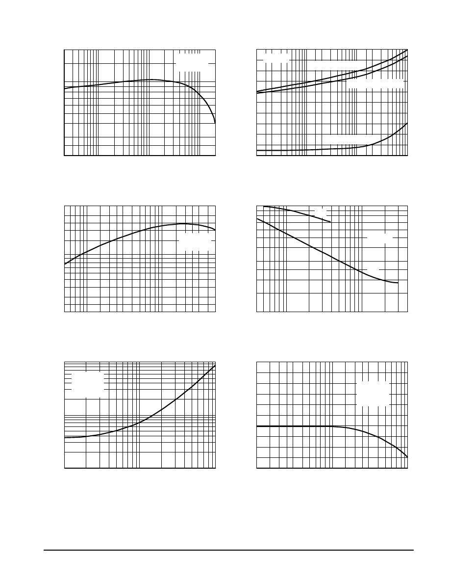
TYPICAL CHARACTERISTICS
2.0
1.5
1.0
0.2
0.3
0.5
0.7
–200
–0.2
–0.5
–1.0
–2.0
–5.0
–10
–20
–50
–100
IC, COLLECTOR CURRENT (mAdc)
Figure 1. Normalized DC Current Gain
h
FE
, NORMALIZED DC CURRENT
GAIN
VCE = –10 V
TA = 25
°
C
–1.0
–0.9
–0.8
–0.7
–0.6
–0.5
–0.4
–0.3
–0.2
–0.1
0
–0.1
IC, COLLECTOR CURRENT (mAdc)
Figure 2. “Saturation” and “On” Voltages
V
, VOL
TAGE
(VOL
TS)
TA = 25
°
C
VBE(sat) @ IC/IB = 10
VBE(on) @ VCE = –10 V
VCE(sat) @ IC/IB = 10
400
20
30
40
60
80
100
200
300
IC, COLLECTOR CURRENT (mAdc)
Figure 3. Current–Gain — Bandwidth Product
f T
, CURRENT–GAIN — BANDWIDTH PRODUCT
(MHz)
C, CAP
ACIT
ANCE
(pF)
10
1.0
2.0
3.0
5.0
7.0
–0.4
VR, REVERSE VOLTAGE (VOLTS)
Figure 4. Capacitances
TA = 25
°
C
Cib
Cob
r b
, BASE SPREADING RESIST
ANCE
(OHMS)
150
140
130
120
110
100
IC, COLLECTOR CURRENT (mAdc)
Figure 5. Output Admittance
–0.2
–0.5
–1.0
–2.0
–5.0
–10
–20
–50
–100
VCE = –10 V
TA = 25
°
C
–0.5
–1.0
–2.0 –3.0
–5.0
–10
–20 –30
–50
–0.6
–1.0
–2.0
–4.0
–6.0
–10
–20 –30 –40
1.0
IC, COLLECTOR CURRENT (mAdc)
Figure 6. Base Spreading Resistance
VCE = –10 V
f = 1.0 kHz
TA = 25
°
C
′
–0.1
–0.2 –0.3
–0.5
–1.0
–2.0 –3.0
–5.0
–10
VCE = –10 V
f = 1.0 kHz
TA = 25
°
C
–0.1
–0.2
–0.5
–1.0
–2.0
–5.0
–10
0.01
0.03
0.05
0.1
0.3
0.5
h , OUTPUT
ADMITT
ANCE
(OHMS)
ob
150
4
Motorola Small–Signal Transistors, FETs and Diodes Device Data
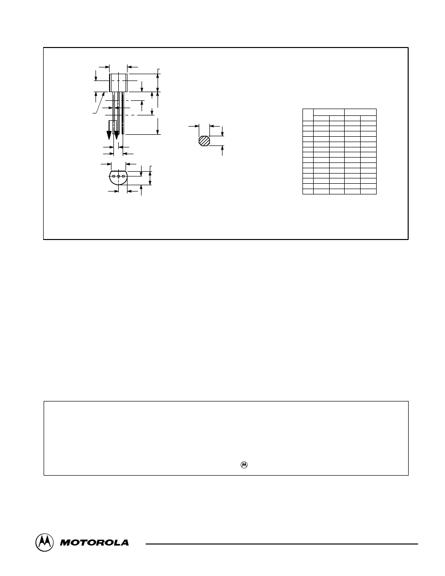
PACKAGE DIMENSIONS
NOTES:
1. DIMENSIONING AND TOLERANCING PER ANSI
Y14.5M, 1982.
2. CONTROLLING DIMENSION: INCH.
3. CONTOUR OF PACKAGE BEYOND DIMENSION R
IS UNCONTROLLED.
4. DIMENSION F APPLIES BETWEEN P AND L.
DIMENSION D AND J APPLY BETWEEN L AND K
MINIMUM. LEAD DIMENSION IS UNCONTROLLED
IN P AND BEYOND DIMENSION K MINIMUM.
R
A
P
J
L
F
B
K
G
H
SECTION X–X
C
V
D
N
N
X X
SEATING
PLANE
DIM
MIN
MAX
MIN
MAX
MILLIMETERS
INCHES
A
0.175
0.205
4.45
5.20
B
0.170
0.210
4.32
5.33
C
0.125
0.165
3.18
4.19
D
0.016
0.022
0.41
0.55
F
0.016
0.019
0.41
0.48
G
0.045
0.055
1.15
1.39
H
0.095
0.105
2.42
2.66
J
0.015
0.020
0.39
0.50
K
0.500
–––
12.70
–––
L
0.250
–––
6.35
–––
N
0.080
0.105
2.04
2.66
P
–––
0.100
–––
2.54
R
0.115
–––
2.93
–––
V
0.135
–––
3.43
–––
1
CASE 029–04
(TO–226AA)
ISSUE AD
STYLE 17:
PIN 1. COLLECTOR
2. BASE
3. EMITTER
Motorola reserves the right to make changes without further notice to any products herein. Motorola makes no warranty, representation or guarantee regarding
the suitability of its products for any particular purpose, nor does Motorola assume any liability arising out of the application or use of any product or circuit, and
specifically disclaims any and all liability, including without limitation consequential or incidental damages. “Typical” parameters which may be provided in Motorola
data sheets and/or specifications can and do vary in different applications and actual performance may vary over time. All operating parameters, including “Typicals”
must be validated for each customer application by customer’s technical experts. Motorola does not convey any license under its patent rights nor the rights of
others. Motorola products are not designed, intended, or authorized for use as components in systems intended for surgical implant into the body, or other
applications intended to support or sustain life, or for any other application in which the failure of the Motorola product could create a situation where personal injury
or death may occur. Should Buyer purchase or use Motorola products for any such unintended or unauthorized application, Buyer shall indemnify and hold Motorola
and its officers, employees, subsidiaries, affiliates, and distributors harmless against all claims, costs, damages, and expenses, and reasonable attorney fees
arising out of, directly or indirectly, any claim of personal injury or death associated with such unintended or unauthorized use, even if such claim alleges that
Motorola was negligent regarding the design or manufacture of the part. Motorola and are registered trademarks of Motorola, Inc. Motorola, Inc. is an Equal
Opportunity/Affirmative Action Employer.
Mfax is a trademark of Motorola, Inc.
How to reach us:
USA / EUROPE / Locations Not Listed: Motorola Literature Distribution;
JAPAN: Nippon Motorola Ltd.: SPD, Strategic Planning Office, 4–32–1,
P.O. Box 5405, Denver, Colorado 80217. 303–675–2140 or 1–800–441–2447
Nishi–Gotanda, Shinagawa–ku, Tokyo 141, Japan. 81–3–5487–8488
Mfax
: RMFAX0@email.sps.mot.com – TOUCHTONE 602–244–6609
ASIA/PACIFIC: Motorola Semiconductors H.K. Ltd.; 8B Tai Ping Industrial Park,
– US & Canada ONLY 1–800–774–1848
51 Ting Kok Road, Tai Po, N.T., Hong Kong. 852–26629298
INTERNET: http://motorola.com/sps
BC307/D
◊
Wyszukiwarka
Podobne podstrony:
BC307
bc307
BC307
BC307, BC308, BC309 (KEC)
BC307 (Philips)
BC307, BC308, BC309 (Motorola)
więcej podobnych podstron