2002 Microchip Technology Inc.
Preliminary
DS39592B-page 1
M
PIC18FX220/X320
1.0
DEVICE OVERVIEW
This document includes the programming specifications
for the following devices:
2.0
PROGRAMMING OVERVIEW
These devices can be programmed using the high volt-
age In-Circuit Serial Programming
TM
(ICSP
TM
) method,
or the low voltage ICSP method; both while in the
user’s system. The low voltage ICSP method is slightly
different than the high voltage method and these differ-
ences are noted where applicable. This programming
specification applies to these devices in all package
types.
2.1
Hardware Requirements
In high voltage ICSP mode, these devices require two
programmable power supplies: one for V
DD
and one for
MCLR/V
PP
. Both supplies should have a minimum res-
olution of 0.25V. Refer to Section 6.0 for additional
hardware parameters.
2.1.1
LOW VOLTAGE ICSP
PROGRAMMING
In low voltage ICSP mode, these devices can be pro-
grammed using a V
DD
source in the operating range.
This only means that MCLR/V
PP
does not have to be
brought to a different voltage, but can instead be left at
the normal operating voltage. Refer to Section 6.0 for
additional hardware parameters.
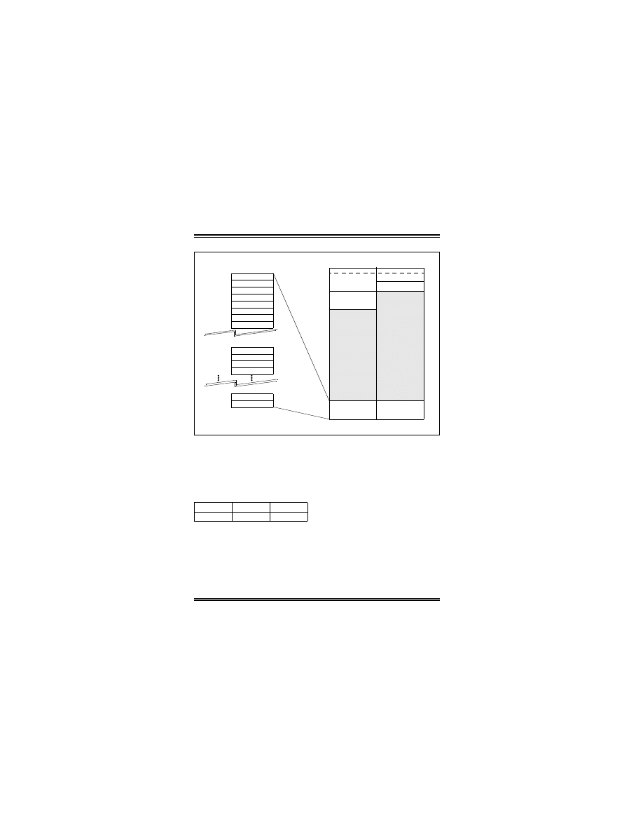
2.2
Pin Diagrams
The programming pin descriptions for these devices
are shown in Table 2-1, and pin diagrams are shown in
Figure 2-1 through Figure 2-3. The pin descriptions of
these diagrams do not represent the complete
functionality of the device types. One should refer to
the appropriate device data sheet for complete pin
descriptions.
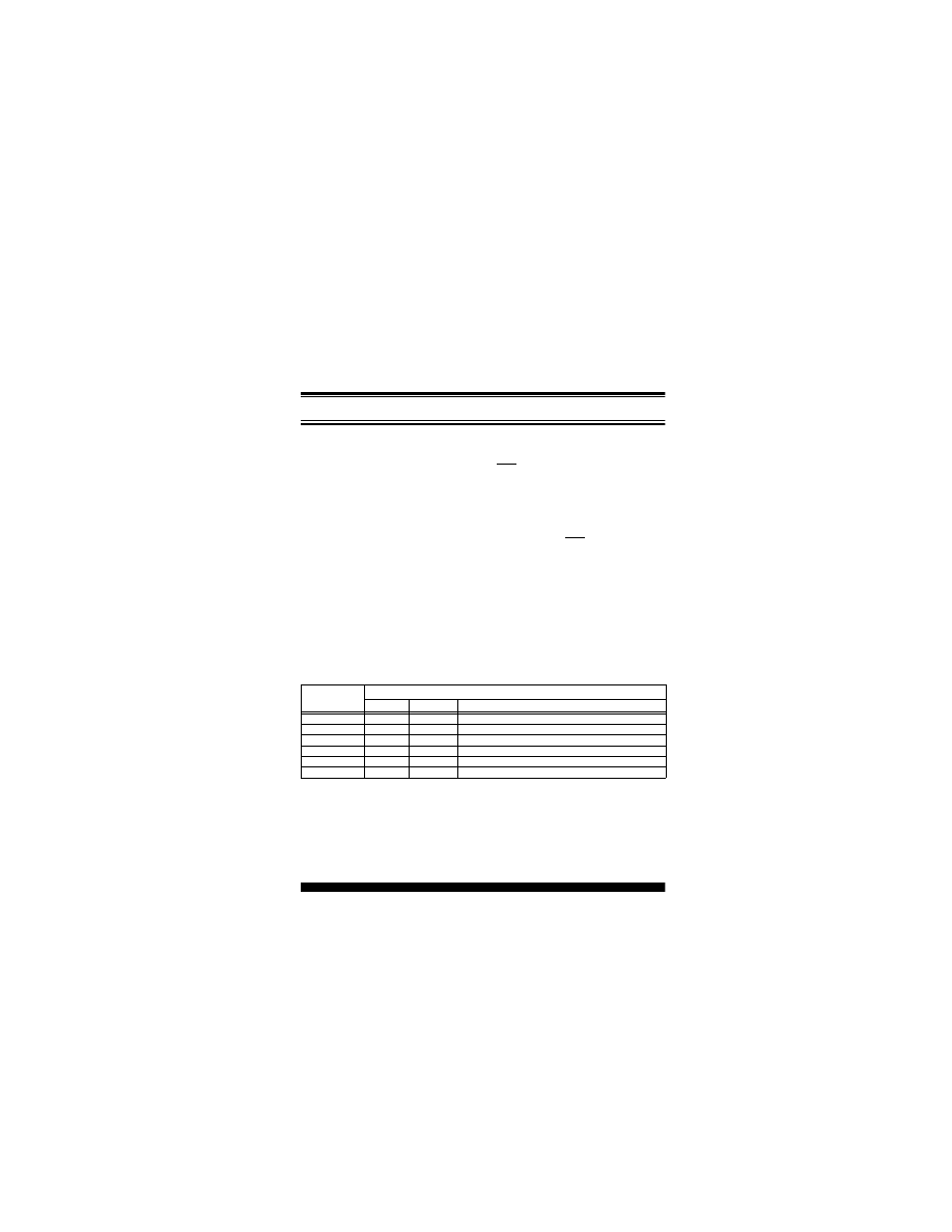
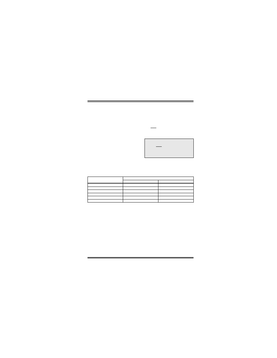
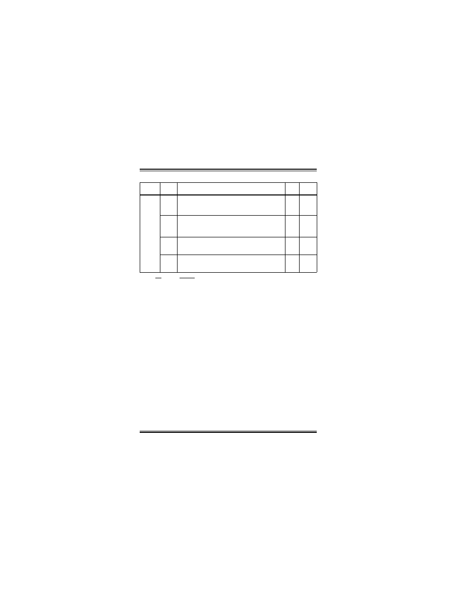
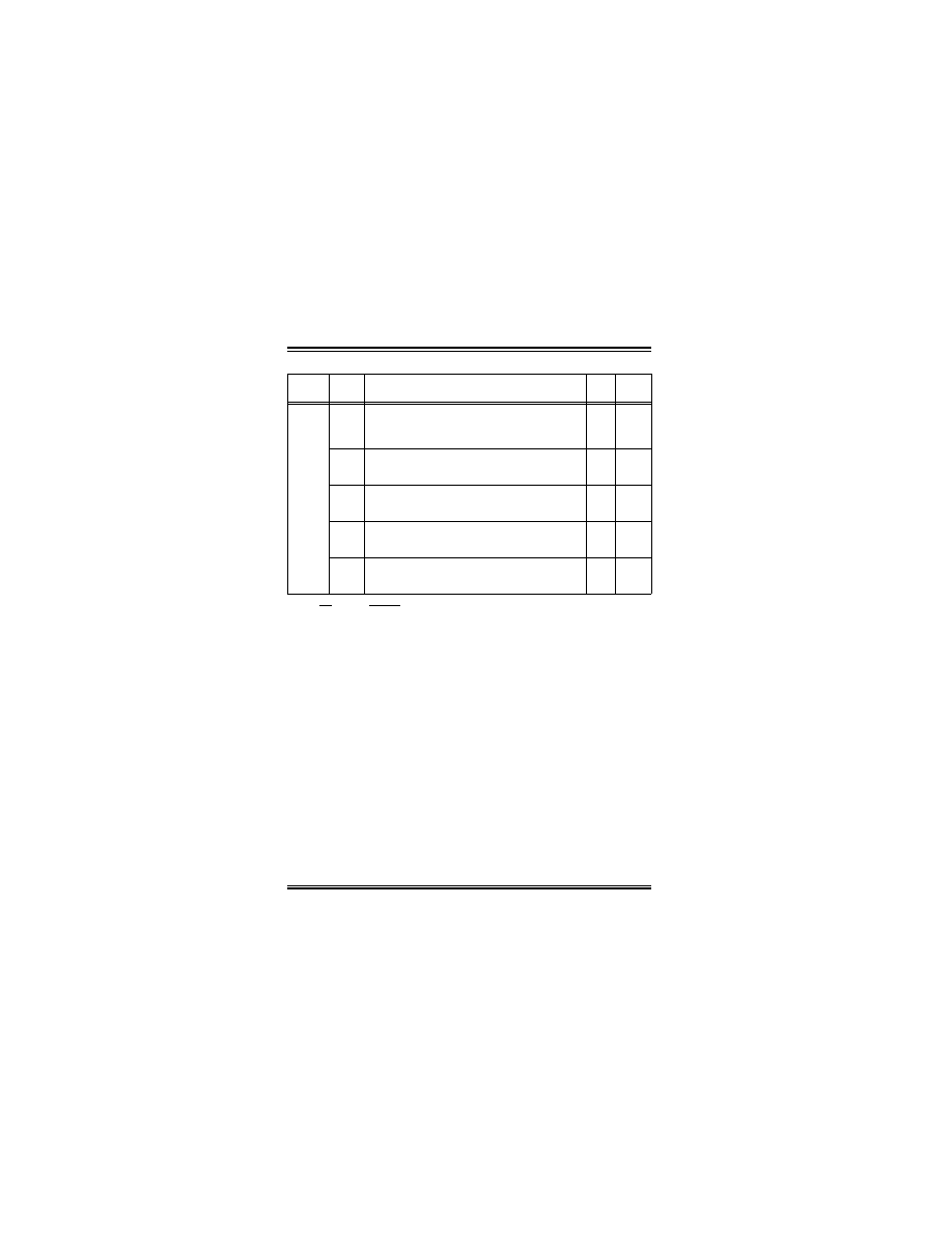
TABLE 2-1:
PIN DESCRIPTIONS (DURING PROGRAMMING)
• PIC18F1220
• PIC18F1320
• PIC18F2220
• PIC18F2320
• PIC18F4220
• PIC18F4320
Pin Name
During Programming
Function
Pin Type
Pin Description
MCLR/V
PP
/RA5
(2)
V
PP
P
High Voltage Programming Enable
V
DD
V
DD
P
Power Supply
V
SS
V
SS
P
Ground
RB5
PGM
I
Low Voltage ICSP Input when LVP
Configuration bit equals ‘1’
(1)
RB6
PGC
I
Serial Clock
RB7
PGD
I/O
Serial Data
Legend: I = Input, O = Output, P = Power
Note 1: See Section 5.3 for more detail.
2: RA5 is only available on the PIC18F1X20.
Programming for PIC18FX220/X320 FLASH MCUs
PIC18FX220/X320
DS39592B-page 2
Preliminary
2002 Microchip Technology Inc.
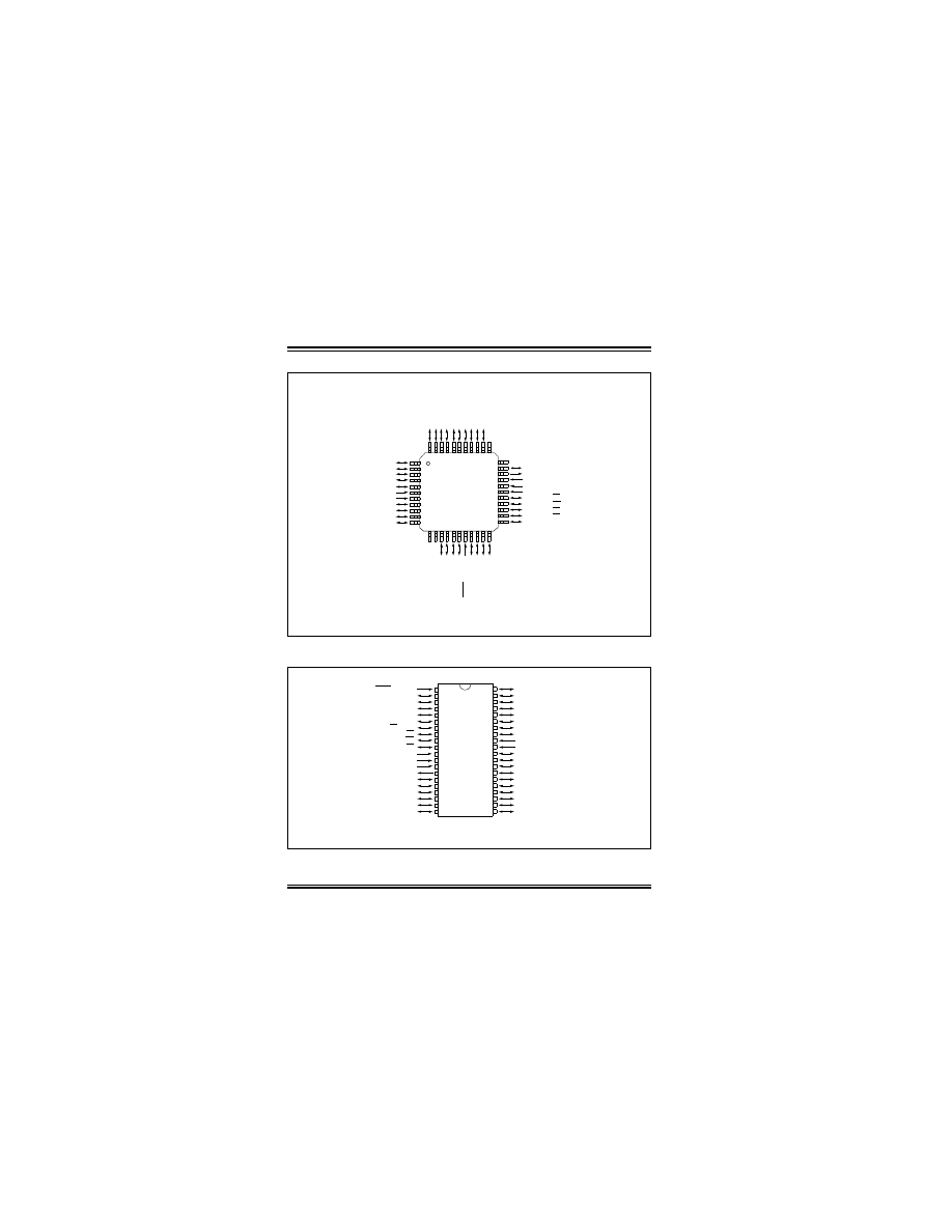
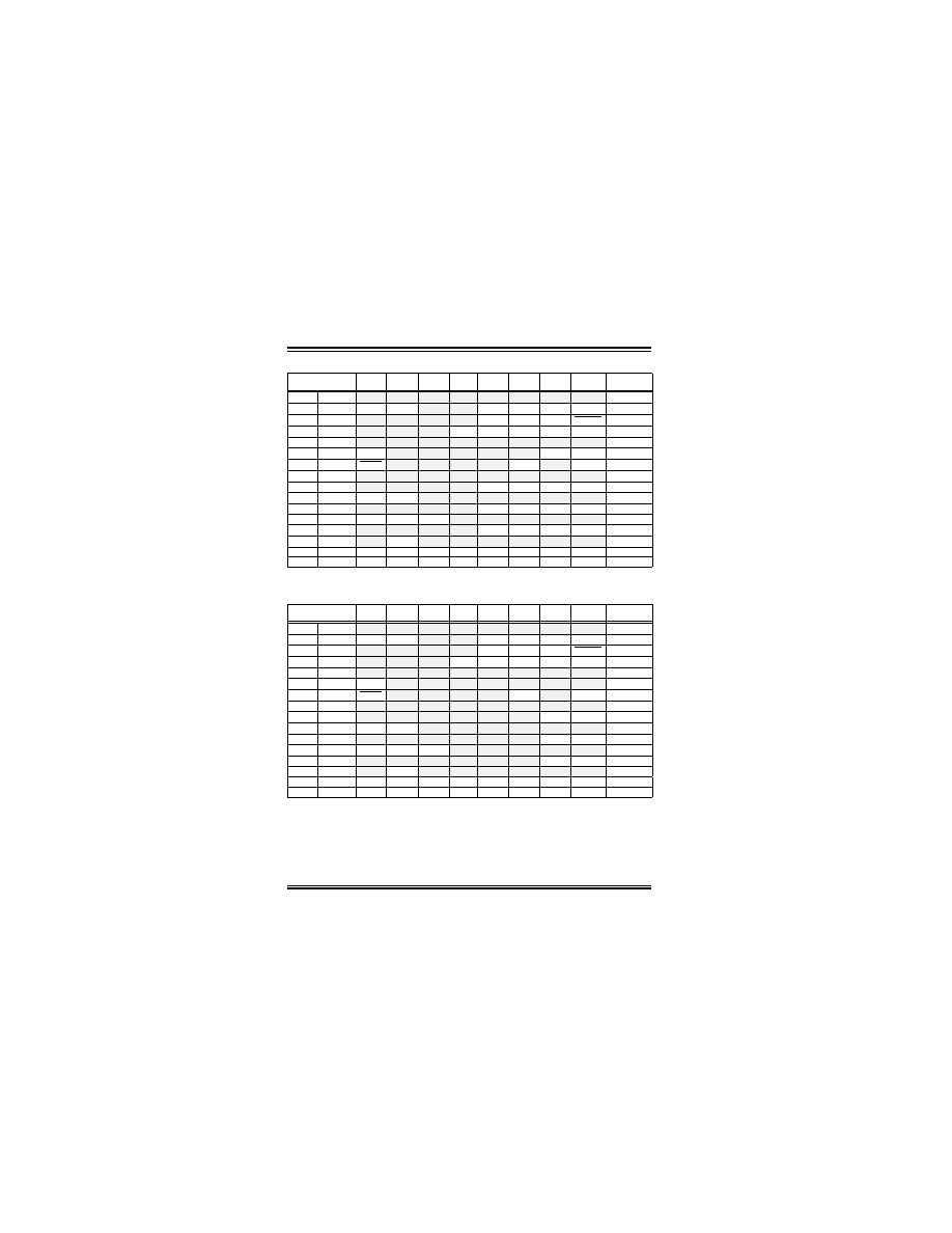
FIGURE 2-1:
PIC18F4X20 44-PIN TQFP
FIGURE 2-2:
PIC18F4X20 40-PIN PDIP (600 MIL)
* Alternate pinout for CCP2 is enabled by a fuse.
10
11
2
3
6
1
18
19
20
21
22
12
13
14
15
38
8
7
44
43
42
41
40
39
16
17
29
30
31
32
33
23
24
25
26
27
28
36
34
35
9
PIC18F4X20
37
R
A
3/A
N
3/V
RE
F
+
RA
2
/A
N
2
/V
RE
F
-/
C
V
RE
F
-
RA
1
/A
N
1
RA
0
/A
N
0
MC
L
R
/V
PP
/RE
3
NC
RB
7
/K
B
I3/P
G
D
RB
6
/K
B
I2/P
G
C
RB
5/K
B
I1
/P
G
M
R
B
4
/AN
1
1
/K
BI
0
NC
RC6
/T
X
/CK
RC5
/S
D
O
R
C
4
/SD
I/
SD
A
R
D
3
/PS
P3
R
D
2
/PS
P2
R
D
1
/PS
P1
R
D
0
/PS
P0
R
C
3
/SC
K
/SC
L
RC2
/CCP
1
/P
1
A
RC1
/T
1
O
S
I/CCP
2
NC
NC
RC0/T1OSO/T1CKI
OSC2/CLKO/RA6
OSC1/CLKI/RA7
V
SS
V
DD
RE2/AN7/CS
RE1/AN6/WR
RE0/AN5/RD
RA5/AN4/SS/LVDIN/C2OUT
RA4/T0CKI/C1OUT
RC7/RX/DT
RD4/PSP4
RD5/PSP5/P1B
RD6/PSP6/P1C
V
SS
V
DD
RB0/AN12/INT0
RB1/AN10/INT1
RB2/AN8/INT2
RB3/AN9/CCP2*
RD7/PSP7/P1D
5
4
* Alternate pinout for CCP2 is enabled by a fuse.
RB7/KBI3/PGD
RB6/KBI2/PGC
RB5/KBI1/PGM
RB4/AN11/KBI0
RB3/AN9/CCP2*
RB2/AN8/INT2
RB1/AN10/INT1
RB0/AN12/INT0
V
DD
V
SS
RD7/PSP7/P1D
RD6/PSP6/P1C
RD5/PSP5/P1B
RD4/PSP4
RC7/RX/DT
RC6/TX/CK
RC5/SDO
RC4/SDI/SDA
RD3/PSP3
RD2/PSP2
MCLR/V
PP
/RE3
RA0/AN0
RA1/AN1
RA2/AN2/V
REF
-/C
VREF
RA3/AN3/V
REF
+
RA4/T0CKI
RA5/AN4/SS/LVDIN
RE0/AN5/RD
RE1/AN6/WR
RE2/AN7/CS
V
DD
V
SS
OSC1/CLKI/RA7
OSC2/CLKO/RA6
RC0/T1OSO/T13CKI
RC1/T1OSI/CCP2
RC2/CCP1/P1A
RC3/SCK/SCL
RD0/PSP0
RD1/PSP1
1
2
3
4
5
6
7
8
9
10
11
12
13
14
15
16
17
18
19
20
40
39
38
37
36
35
34
33
32
31
30
29
28
27
26
25
24
23
22
21
PI
C18
F
4X20
2002 Microchip Technology Inc.
Preliminary
DS39592B-page 3
PIC18FX220/X320
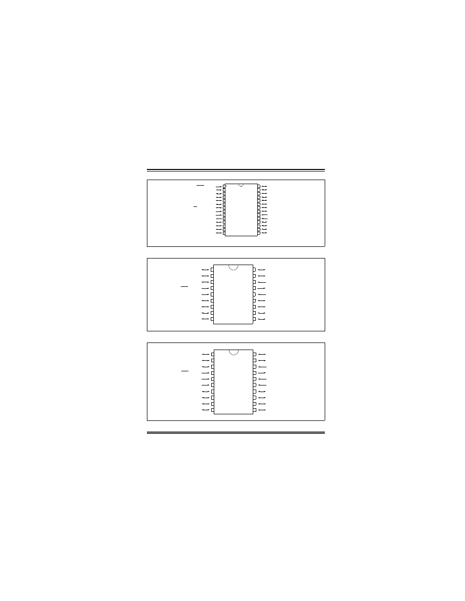
FIGURE 2-3:
PIC18F2X20 28-PIN SDIP (300 MIL), SOIC
FIGURE 2-4:
PIC18F1X20 18-PIN PDIP, SOIC
FIGURE 2-5:
PIC18F1X20 20-PIN SSOP
10
11
2
3
4
5
6
1
8
7
9
12
13
14
15
16
17
18
19
20
23
24
25
26
27
28
22
21
MCLR/V
PP
/RE3
RA0/AN0
RA1/AN1
RA2/AN2/V
REF
-/C
VREF
RA3/AN3/V
REF
+
RA4/T0CKI/C1OUT
RA5/AN4/SS/LVDIN/C2OUT
V
SS
OSC1/CLKI/RA7
OSC2/CLKO/RA6
RC0/T1OSO/T13CKI
RC1/T1OSI/CCP2
RC2/CCP1
RC3/SCK/SCL
RB7/KBI3/PGD
RB6/KBI2/PGC
RB5/KBI1/PGM
RB4/AN11/KBI0
RB3/AN9/CCP2*
RB2/AN8/INT2
RB1/AN10/INT1
RB0/AN12/INT0
V
DD
V
SS
RC7/RX/DT
RC6/TX/CK
RC5/SDO
RC4/SDI/SDA
* Alternate pinout for CCP2 is enabled by a fuse.
PI
C18F2
X
20
RB3/CCP1A/P1A
RB2/P1B/INT2
OSC1/CLKI/RA7
OSC2/CLKO/RA6
V
DD
/AV
DD
RB7/PGD/T1OSI/P1D
RB6/PGC/T1OSO/T1CKI/P1C
RB5/PGM
RB4/AN6/RX/DT
RA0/AN0
RA1/AN1/LVDIN
RA4/T0CKI
MCLR/V
PP
/RA5
Vss/AVss
RA2/AN2/V
REF
-
RA3/AN3/V
REF
+
RB0/AN4/INT0
RB1/AN5/TX/CK/INT1
1
2
3
4
5
6
7
8
9
18
17
16
15
14
13
12
11
10
PI
C18F
1X20
RB3/CCP1A/P1A
RB2/P1B/INT2
OSC1/CLKI/RA7
OSC2/CLKO/RA6
V
DD
RB7/PGD/T1OSI/P1D
RB6/PGC/T1OSO/T1CKI/P1C
RB5/PGM
RB4/AN6/RX/DT
RA0/AN0
RA1/AN1/LVDIN
RA4/T0CKI
MCLR/V
PP
/RA5
V
SS
RA2/AN2/V
REF
-
RA3/AN3/V
REF
+
RB0/AN4/INT0
RB1/AN5/TX/CK/INT1
1
2
3
4
5
7
8
9
10
20
19
18
17
16
14
13
12
11
PI
C18F1
X
20
AV
DD
AV
SS
6
15
PIC18FX220/X320
DS39592B-page 4
Preliminary
2002 Microchip Technology Inc.
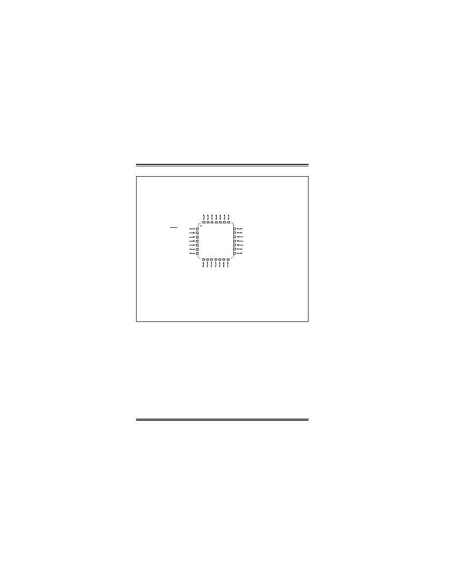
FIGURE 2-6:
PIC18F1X20 28-PIN QFN
16
2
RA
0
/A
N
0
R
B
2
/P1
B/
IN
T
2
RA
4
/T
0
CK
I
MCLR/V
PP
/RA5
NC
AV
SS
NC
RA2/AN2/V
REF
-
R
A
3/A
N
3/
V
RE
F
+
R
A
1/A
N
1
/LV
D
IN
RA7/OSC1/CLKI
RA6/OSC2/CLKO
V
DD
NC
AV
DD
RB7/PGD/T1OSI/P1D/KBI3
RB6/PGC/T1OSO/T1CKI/P1C/KBI2
RB
5
/P
G
M
/K
B
I1
R
B
4/
A
N
6/R
X
/D
T
/K
B
I0
7
PIC18F1X20
1
3
6
5
4
15
21
19
20
17
18
22
28
26
27
23
24
25
14
8
10
9
13
12
11
V
SS
NC
NC
RB
3
/CCP
1
A
RB
0
/A
N
4
/I
N
T
0
R
B
1
/AN
5
/T
X
/C
K/
IN
T
1
NC
NC
NC

2002 Microchip Technology Inc.
Preliminary
DS39592B-page 5
PIC18FX220/X320
2.3
Memory Map
The code memory space extends from 0000h to 1FFFh
(8 Kbytes) in a single 8-Kbyte panel. Addresses 0000h
through 01FFh, however, define a “Boot Block” region
that is treated separately from Panel 1. All code
memory is on-chip.
A user may store identification information (ID) in eight
ID registers. These ID registers are mapped in
addresses 200000h through 200007h. The ID locations
read out normally, even after code protection is applied.
Locations 300001h through 30000Dh are reserved for
the configuration words. These words may be set to
select various device options, and are described in
Section 5.0. These configuration words read out
normally, even after code protected.
Locations 3FFFFEh and 3FFFFFh are reserved for the
device ID words. These words may be used by the pro-
grammer to identify what device type is being pro-
grammed, and are described in Section 5.0. These
configuration words read out normally, even after code
protection.
TABLE 2-2:
IMPLEMENTATION OF CODE MEMORY
FIGURE 2-7:
MEMORY MAP FOR PIC18F2X20/PIC18F4X20
Device
Code Memory Size (Bytes)
Data EEPROM Size (Bytes)
PIC18F1220
0000h - 0FFFh (4K)
000 - 0FFh (256)
PIC18F2220
0000h - 0FFFh (4K)
000 - 0FFh (256)
PIC18F4220
0000h - 0FFFh (4K)
000 - 0FFh (256)
PIC18F1320
0000h - 1FFFh (8K)
000 - 0FFh (256)
PIC18F2320
0000h - 1FFFh (8K)
000 - 0FFh (256)
PIC18F4320
0000h - 1FFFh (8K)
000 - 0FFh (256)
0000h
200000h
3FFFFFh
Unimplemented
Read as 0’s
200h
07FFh
Boot Block
Block 0
8 Kbytes
200000h
ID Location 1
200001h
ID Location 2
200002h
ID Location 3
200003h
ID Location 4
200004h
ID Location 5
200005h
ID Location 6
200006h
ID Location 7
200007h
ID Location 8
300000h
CONFIG1L
300001h
CONFIG1H
300002h
CONFIG2L
300003h
CONFIG2H
3FFFFEh
Device ID1
3FFFFFh
Device ID2
4 Kbytes
Block 0
Block 1
Boot Block
Block 1
Block 2
Block 3
0FFFh
17FFh
1FFFh
Unimplemented
Read as 0’s
PIC18FX220/X320
DS39592B-page 6
Preliminary
2002 Microchip Technology Inc.
FIGURE 2-8:
MEMORY MAP FOR PIC18F1X20
2.3.1
MEMORY ADDRESS POINTER
Memory in the address space 000000h to 3FFFFFh is
addressed via the Table Pointer, which is comprised of
three pointer registers:
• TBLPTRU, at address 0FF8h
• TBLPTRH, at address 0FF7h
• TBLPTRL, at address 0FF6h
2.4
High Level Overview of the
Programming Process
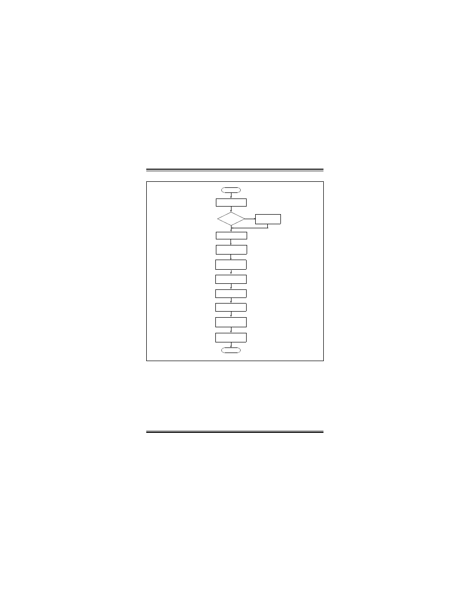
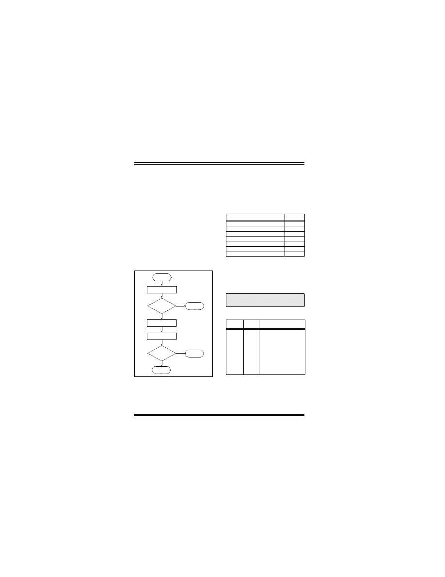
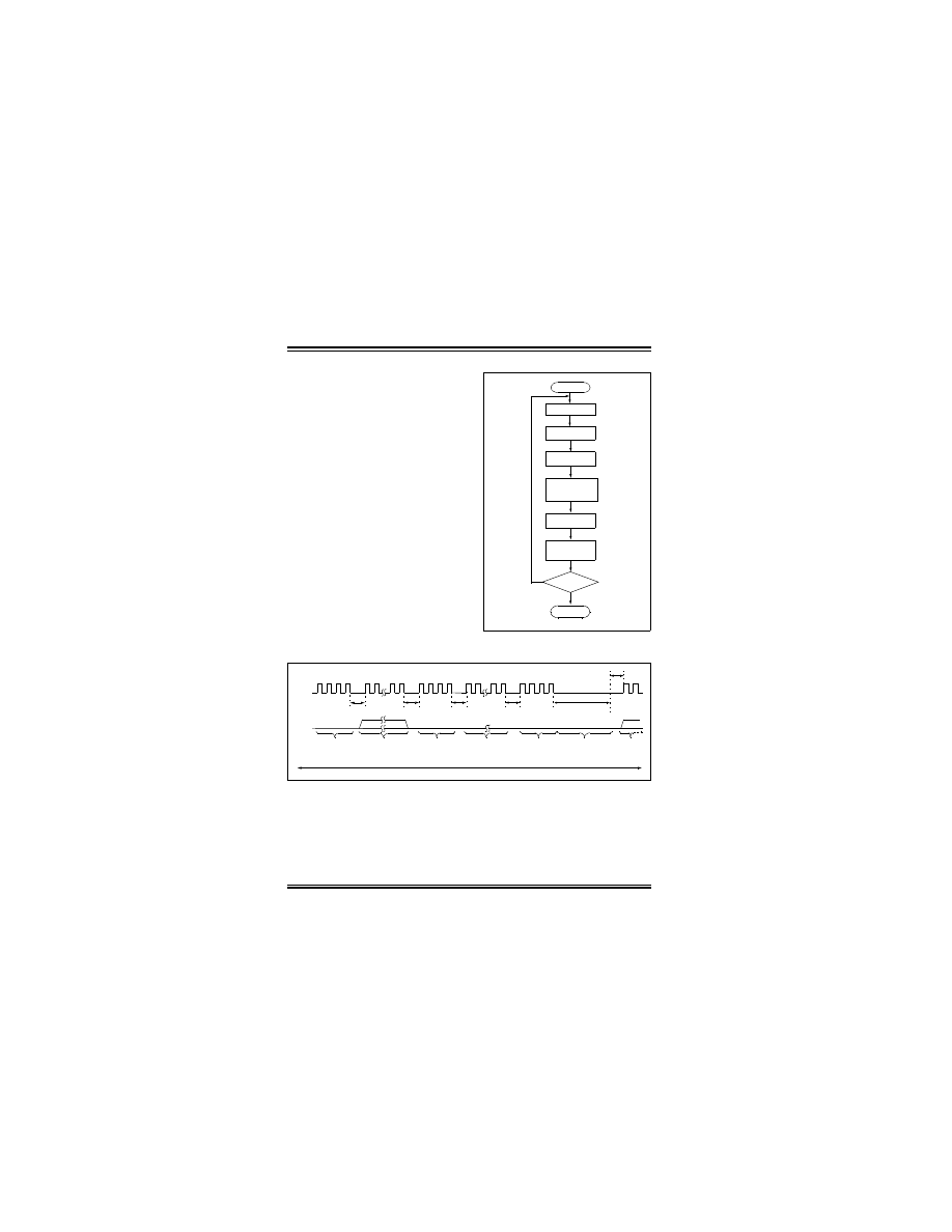
Figure 2-9 shows the high level overview of the Pro-
gramming Process. The device is first checked to see
if it is blank; if it is not, a bulk erase is performed. Next,
the Program Memory, ID locations and Data EEPROM
are written. These memories are then verified to ensure
that programming was successful. If no errors are
detected, the configuration bits are then written and
verified.
0000h
200000h
3FFFFFh
Unimplemented
Read as 0’s
200h
07FFh
Boot Block
Block 0
8 Kbytes
200000h
ID Location 1
200001h
ID Location 2
200002h
ID Location 3
200003h
ID Location 4
200004h
ID Location 5
200005h
ID Location 6
200006h
ID Location 7
200007h
ID Location 8
300000h
CONFIG1L
300001h
CONFIG1H
300002h
CONFIG2L
300003h
CONFIG2H
3FFFFEh
Device ID1
3FFFFFh
Device ID2
4 Kbytes
Block 0
Block 1
Boot Block
Block 1
0FFFh
17FFh
1FFFh
Unimplemented
Read as 0’s
TBLPTRU
TBLPTRH
TBLPTRL
Addr[21:16]
Addr[15:8]
Addr[7:0]
2002 Microchip Technology Inc.
Preliminary
DS39592B-page 7
PIC18FX220/X320
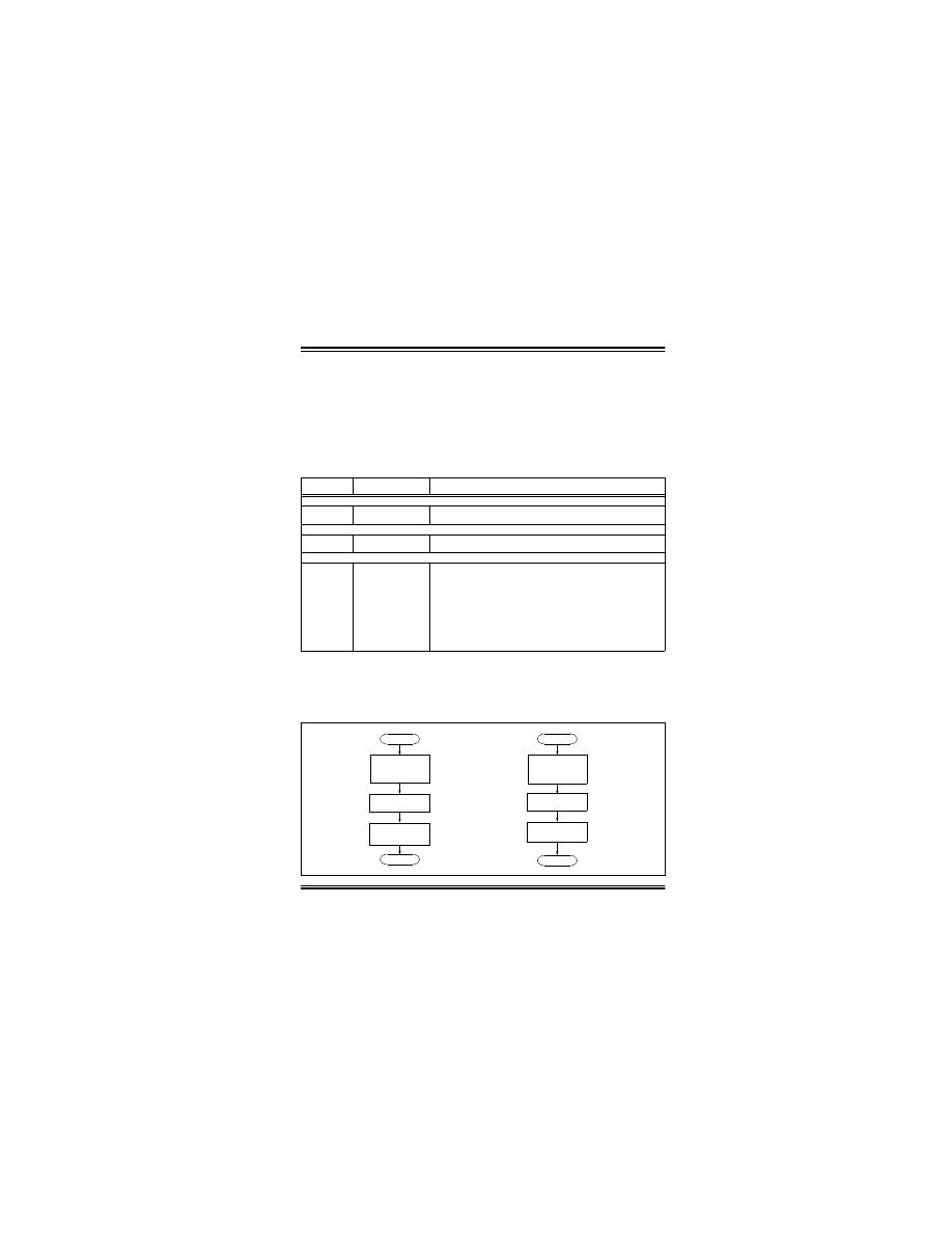
FIGURE 2-9:
HIGH LEVEL PROGRAMMING FLOW
Start
Program Memory
Write ID Loc’s
Write EEPROM
Verify Program
Verify IDs
Verify EEPROM
Write
Configuration Bits
Verify
Configuration Bits
Done
Is part blank
?
No
Perform Bulk
Erase
Yes
Blank Check
Write
PIC18FX220/X320
DS39592B-page 8
Preliminary
2002 Microchip Technology Inc.
2.5
Entering High Voltage ICSP
Program/Verify Mode
The high voltage ICSP Program/Verify mode is entered
by holding PGC and PGD low, and then raising MCLR/
V
PP
to V
IHH
(high voltage). Once in this mode, the Code
Memory, Data EEPROM, ID locations and configura-
tion bits can be accessed and written in serial fashion.
The sequence that enters the device into the Program-
ming/Verify mode places all unused I/Os in the high
impedance state.
FIGURE 2-10:
ENTERING HIGH VOLTAGE
PROGRAM/ VERIFY MODE
2.5.1
ENTERING LOW VOLTAGE ICSP
PROGRAM/VERIFY MODE
When the LVP configuration bit is 1 (see Section 5.3),
the low voltage ICSP mode is enabled. Low voltage
ICSP Program/Verify mode is entered by holding PGC
and PGD low, placing a logic high on PGM, and then
raising MCLR/V
PP
to V
IH
. In this mode, the RB5/PGM
pin is dedicated to the programming function and
ceases to be a general purpose I/O pin.
The sequence that enters the device into the Program-
ming/Verify mode places all unused I/Os in the high
impedance state.
FIGURE 2-11:
ENTERING LOW VOLTAGE
PROGRAM/ VERIFY MODE
2.6
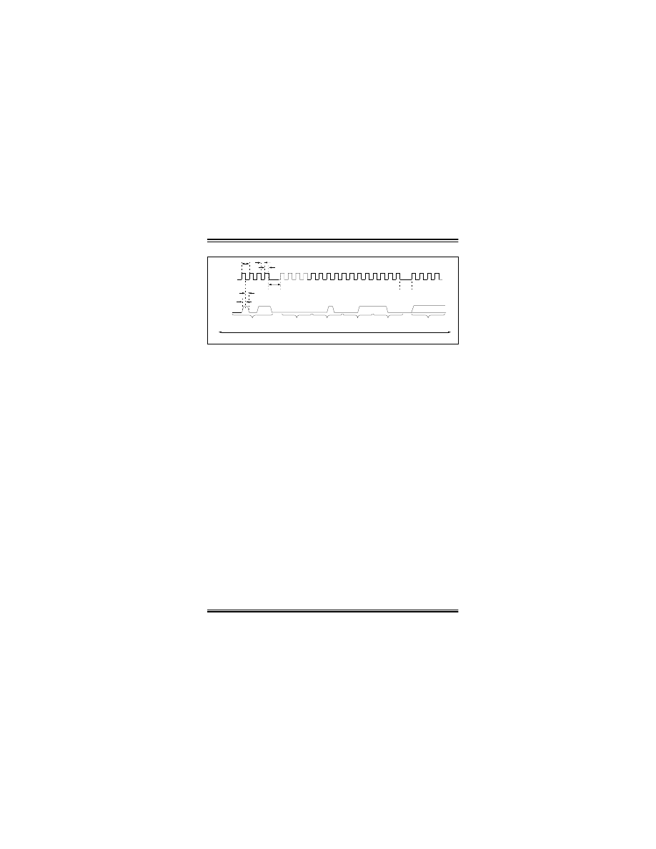
Serial Program/Verify Operation
The PGC pin is used as a clock input pin and the PGD
pin is used for entering command bits and data input/
output during serial operation. Commands and data are
transmitted on the rising edge of PGC, latched on the
falling edge of PGC, and are sent Least Significant bit
(LSb) first.
2.6.1
4-BIT COMMANDS
All instructions are 20-bits, consisting of a leading 4-bit
command followed by a 16-bit operand, which depends
on the type of command being executed. To input a
command, PGC is cycled four times. The commands
needed for programming and verification are shown in
Table 2-3.
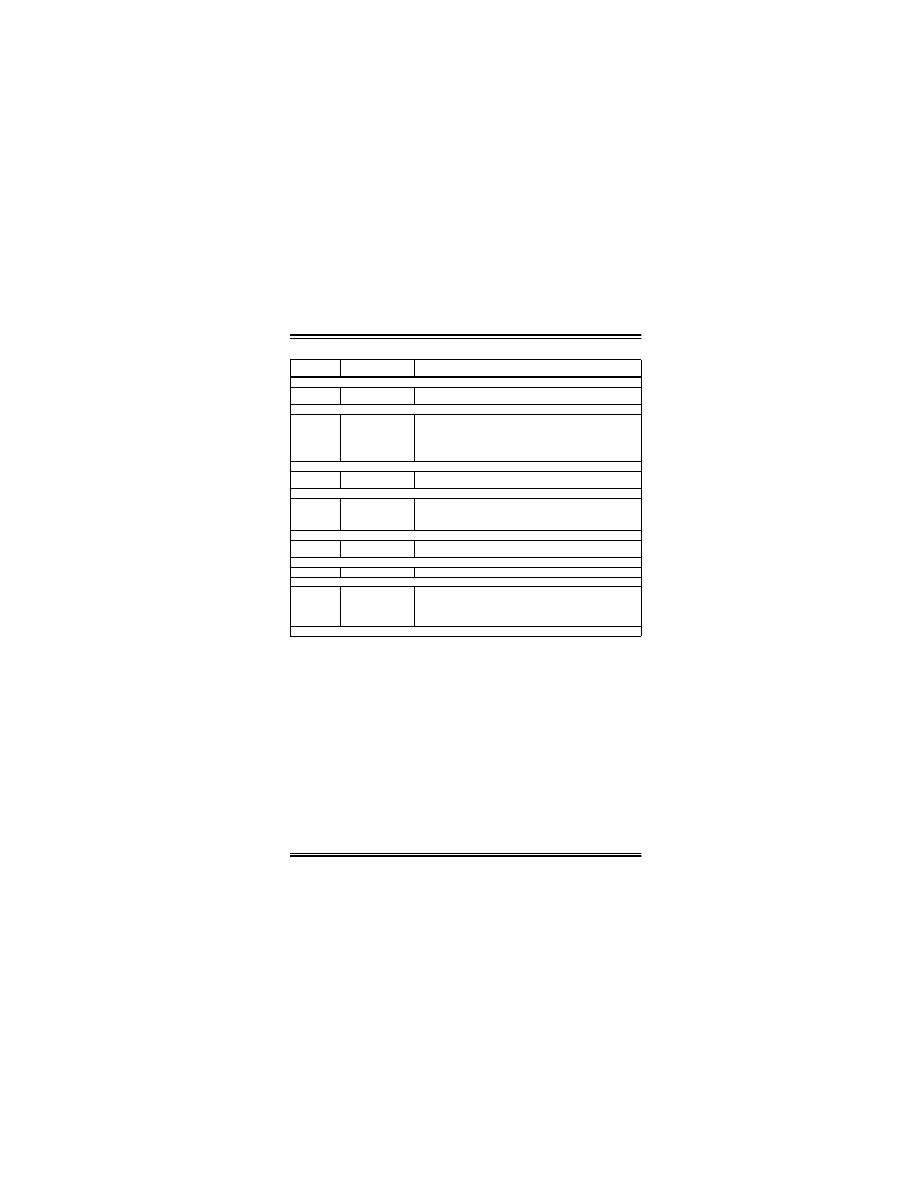
TABLE 2-3:
COMMANDS FOR
PROGRAMMING
Depending on the 4-bit command, the 16-bit operand
represents 16-bits or 8-bits of data.
Throughout this specification, commands and data are
presented as illustrated in Table 2-4. The 4-bit com-
mand is shown MSb first. The command operand, or
“Data Payload” is shown <MSB:LSB>. Figure 2-12
demonstrates how to serially present a 20-bit
command/operand to the device.
TABLE 2-4:
SAMPLE COMMAND
SEQUENCE
MCLR/V
PP
P12
PGD
PGD = Input
PGC
V
DD
D110
P13
MCLR/V
PP
P12
PGD
PGD = Input
PGC
PGM
P15
V
DD
V
IH
V
IH
Description
4-Bit
Command
Core Instruction
(Shift in 16-bit instruction)
0000
Shift out TABLAT register
0010
Table Read
1000
Table Read, post-increment
1001
Table Read, post-decrement
1010
Table Read, pre-increment
1011
Table Write
1100
Table Write, post-increment by 2
1101
Table Write, post-decrement by 2
1110
Table Write, start programming
1111
4-Bit
Command
Data
Payload
Core Instruction
1101
3C 40
Table Write,
post-increment by 2
2002 Microchip Technology Inc.
Preliminary
DS39592B-page 9
PIC18FX220/X320
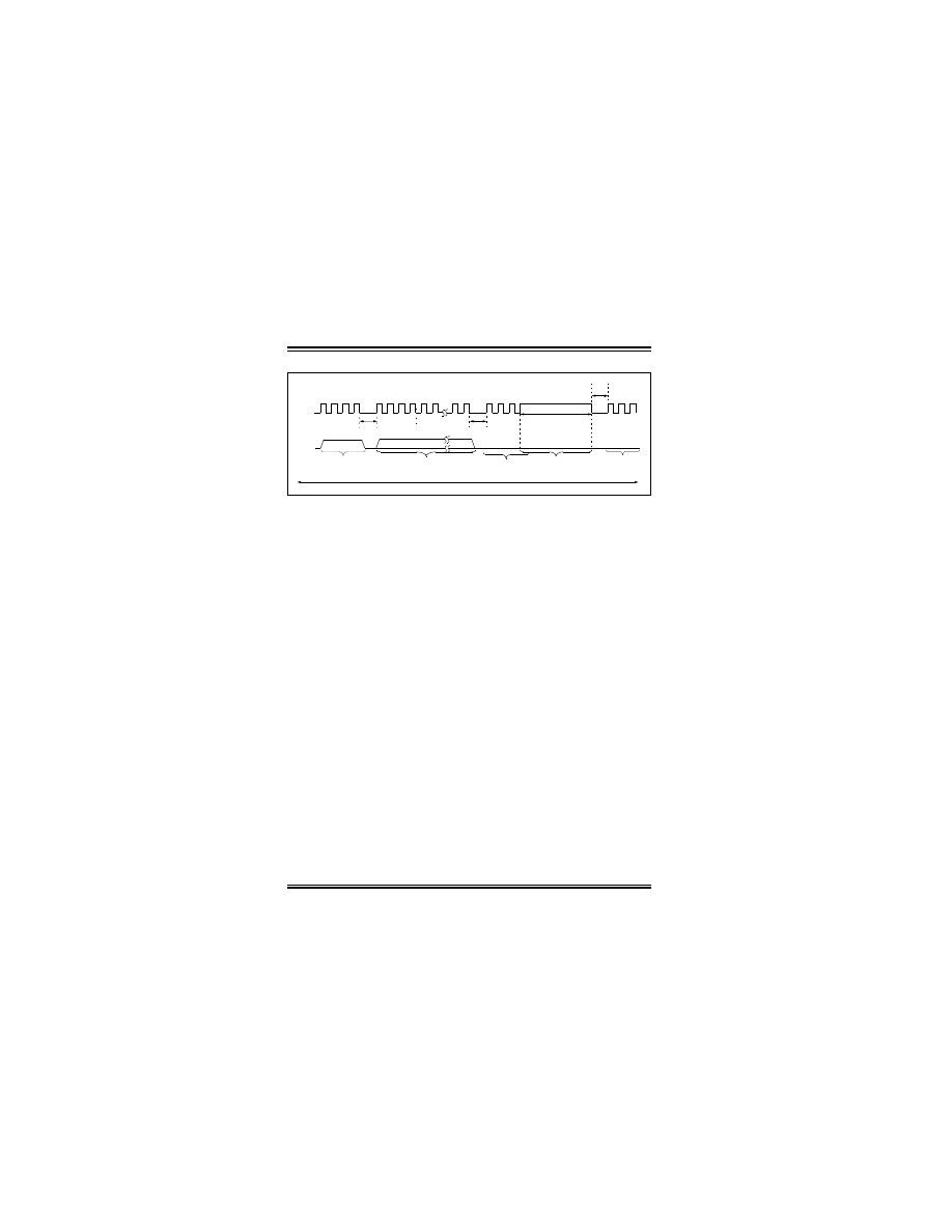
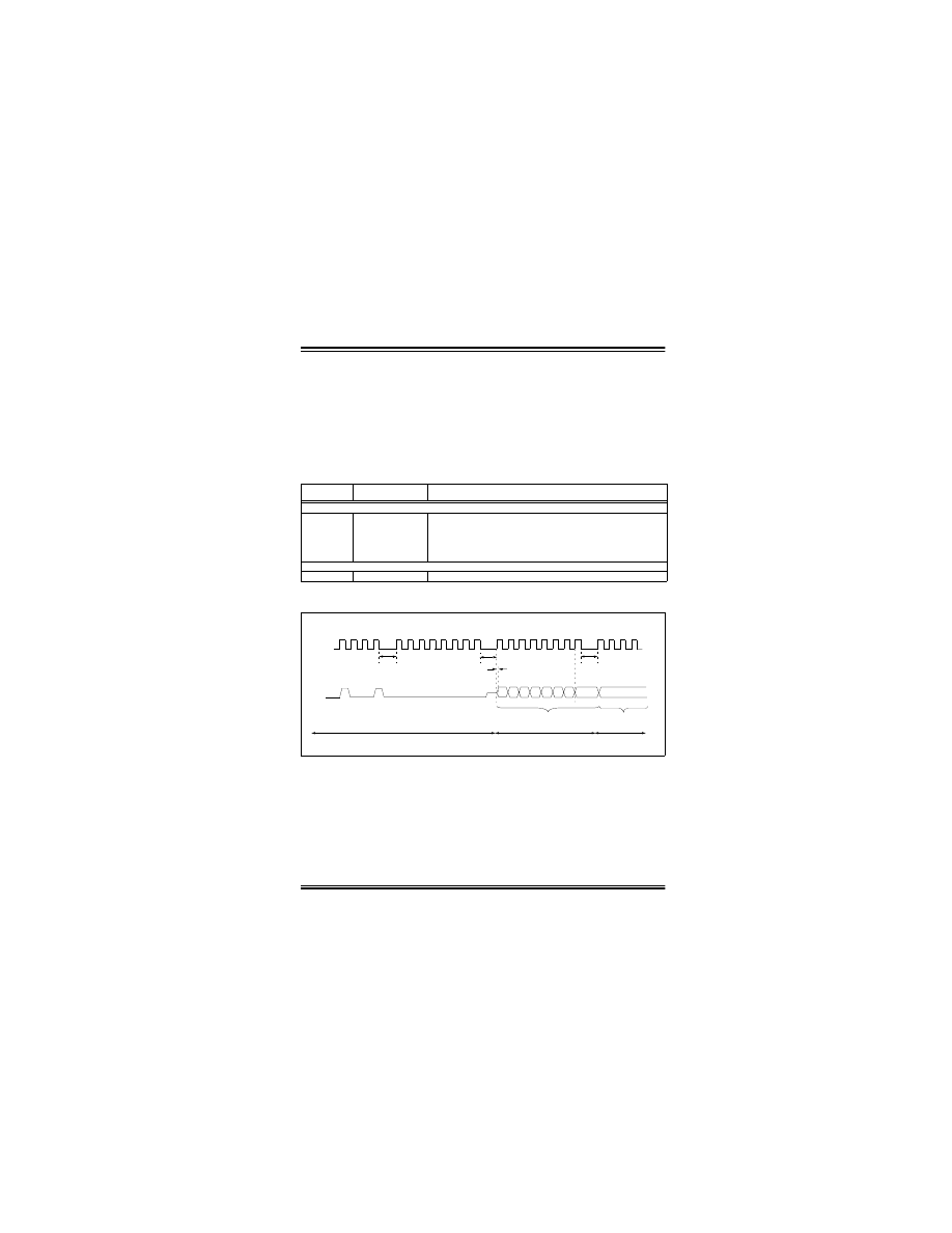
FIGURE 2-12:
TABLE WRITE, POST INCREMENT TIMING
(1101
)
2.6.2
CORE INSTRUCTION
The core instruction passes a 16-bit instruction to the
CPU core for execution. This is needed to setup
registers, as appropriate for use with other commands.
If the instruction is a 1-word, 1-cycle instruction, it will
be executed while the next command is clocked in.
If the instruction is a 2-word, 2-cycle instruction,
another core instruction command is required with the
second word of the instruction. The instruction will
complete when a third 4-bit command has been
loaded.
1
2
3
4
PGC
P5
PGD
PGD = Input
5
6
7
8
1
2
3
4
P5a
9
10
11
13
15
16
14
12
Fetch Next 4-bit Command
1
0
1
1
1
2
3
4
n
n
n
n
P3
P2
P2a
0
0
0
0
0
0
0
1
0
0
0
1
1
1
1
0
0
4
C
3
P4
4-bit Command (LSb first)
16-bit Data Payload (LSb first)
P2b
PIC18FX220/X320
DS39592B-page 10
Preliminary
2002 Microchip Technology Inc.
3.0
DEVICE PROGRAMMING
3.1
Blank Check
The term “Blank Check” means to verify that the device
has no programmed memory cells. All memories must
be verified: Code memory, Data EEPROM, ID locations
and configuration bits. The Device ID registers
(3FFFFEh:3FFFFFh) should be ignored.
A “blank” or “erased” memory cell will read as a ‘1’. So,
“Blank Checking” a device merely means to verify that all
bytes read as FFh, except the configuration bits. Unused
(reserved) configuration bits will read ‘0’ (programmed).
Refer to Table 5-2 for blank configuration expected data
for the various devices.
If it is determined that the device is not blank, then the
device should be Bulk Erased (see Section 3.2) before
any attempt to program is made.
Given that “Blank Checking” is merely code and data
EEPROM verification with FFh as the expected data,
refer to Section 4.1 and Section 4.3 for implementation
details.
FIGURE 3-1:
BLANK CHECK FLOW
3.2
High Voltage ICSP Bulk Erase
Erasing Code or Data EEPROM is accomplished by
writing an “erase option” to address 3C0004h. Code
memory may be erased portions at a time, or the user
may erase the entire device in one action. “Bulk Erase”
operations will also clear any code protect settings
associated with the memory block erased. Erase
options are detailed in Table 3-1.
TABLE 3-1:
BULK ERASE OPTIONS
The actual Bulk Erase function is a self-timed opera-
tion. Once the erase has started (falling edge of the 4th
PGC after the WRITE command), serial execution will
cease until the erase completes (parameter P11). Dur-
ing this time, PGC may continue to toggle, but PGD
must be held low.
The code sequence to erase the entire device is shown
in Table 3-2 and the flow chart is shown in Figure 3-2.
TABLE 3-2:
BULK ERASE COMMAND
SEQUENCE
Is
Yes
No
Start
Blank Check Device
device
blank?
Bulk Erase Device
Blank Check Device
Is
device
blank?
Continue
Abort
No
Yes
Continue
Description
Data
Chip Erase
80h
Erase Data EEPROM
81h
Erase Boot Block
83h
Erase Block 0
88h
Erase Block 1
89h
Erase Block 2
8Ah
Erase Block 3
8Bh
Note:
A bulk erase is the only way to reprogram
code protect bits from an on-state to an
off-state.
4-bit
Command
Data
Payload
Core Instruction
0000
0000
0000
0000
0000
0000
1100
0000
0000
0E 3C
6E F8
0E 00
6E F7
0E 04
6E F6
00 80
00 00
00 00
MOVLW 3Ch
MOVWF TBLPTRU
MOVLW 00h
MOVWF TBLPTRH
MOVLW 04h
MOVWF TBLPTRL
Write 80h TO 3C0004h to
erase entire device.
NOP
Hold PGD low until
erase completes.
2002 Microchip Technology Inc.
Preliminary
DS39592B-page 11
PIC18FX220/X320
FIGURE 3-2:
BULK ERASE FLOW
FIGURE 3-3:
BULK ERASE TIMING
3.2.1
LOW VOLTAGE ICSP BULK ERASE
When using low voltage ICSP, the part must be sup-
plied by the voltage specified in parameter D111, if a
bulk erase is to be executed. All other bulk erase details
as described above apply.
If it is determined that a program memory erase must
be performed at a supply voltage below the bulk erase
limit, refer to the erase methodology described in
Section 3.3.1.
If it is determined that a data EEPROM erase must be
performed at a supply voltage below the bulk erase
limit, follow the methodology described in Section 3.4
and write zeroes to the array.
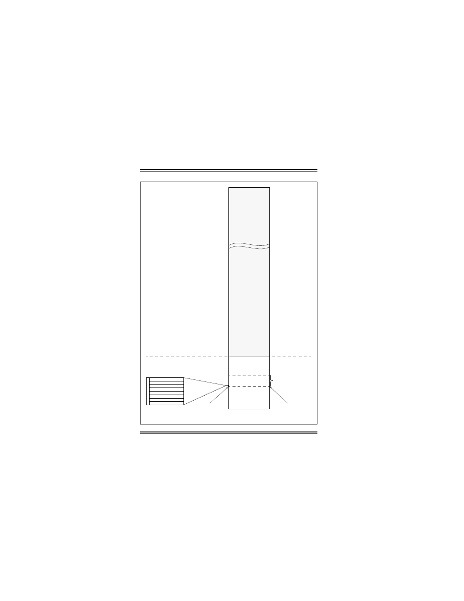
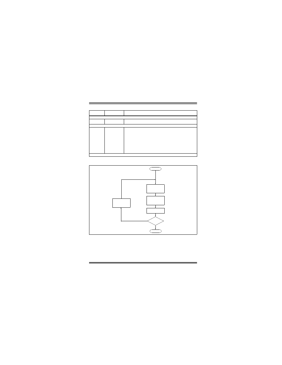
3.3
Code Memory Programming
Programming code memory is accomplished by first
loading data into the appropriate write buffers and then
initiating a programming sequence. Each panel in the
code memory space (see Figure 2-8) has an 8-byte
deep write buffer that must be loaded prior to initiating
a write sequence. The actual memory write sequence
takes the contents of these buffers and programs the
associated EEPROM code memory.
The programming duration is externally timed and is
controlled by PGC. After a “Start Programming” com-
mand is issued (4-bit command
1111
), a
NOP
is issued
where the 4th PGC is held high for the duration of the
programming time, P9 (see Figure 3-6).
After PGC is brought low, the programming sequence
is terminated. PGC must be held low for the time spec-
ified by parameter P10 to allow high voltage discharge
of the memory array.
The code sequence to program a device is shown in
Table 3-3. The flow chart shown in Figure 3-5 depicts
the logic necessary to completely write a device.
Start
Done
Write 80h
to Erase
Entire Device
Load Address
Pointer to
3C0004h
Delay P11+P10
Time
n
1
2
3
4
1
2
15 16
1
2
3
PGC
P5
P5a
PGD
PGD = Input
0
0
0
1
1
P11
P10
Erase Time
0
0
0
0
0
0
0
0
1
2
0
0
4
0
1
2
15 16
P5
1
2
3
P5a
4
0
0
0
0
n
4-bit Command
4-bit Command
4-bit Command
NOP
16-bit
Data Payload
16-bit
Data Payload
Note:
The TBLPTR register must contain the
same offset value when initiating the pro-
gramming sequence as it did when the
write buffers were loaded.
PIC18FX220/X320
DS39592B-page 12
Preliminary
2002 Microchip Technology Inc.
FIGURE 3-4:
ERASE AND WRITE BOUNDARIES
TBLPTR<2:0> = 0
TBLPTR<2:0> = 1
TBLPTR<2:0> = 2
TBLPTR<2:0> = 3
TBLPTR<2:0> = 4
TBLPTR<2:0> = 5
TBLPTR<2:0> = 6
TBLPTR<2:0> = 7
Offset = TBLPTR<12:3>
TBLPTR<21:13> = 0
Offset = TBLPTR<12:6>
Panel 1
Erase Region
(64 bytes)
8-
by
te W
ri
te B
u
ffer
Note: TBLPTR = TBLPTRU:TBLPTRH:TBLPTRL.
Unimplemented
Read as ‘0’
2002 Microchip Technology Inc.
Preliminary
DS39592B-page 13
PIC18FX220/X320
TABLE 3-3:
WRITE CODE MEMORY CODE SEQUENCE
FIGURE 3-5:
PROGRAM CODE MEMORY FLOW
4-bit
Command
Data Payload
Core Instruction
Step 1: Direct access to code memory.
0000
0000
8E A6
9C A6
BSF EECON1, EEPGD
BCF EECON1, CFGS
Step 2: Load write buffer for Panel 1.
0000
0000
0000
0000
0000
0000
1101
1101
1101
1100
0000
0E <Addr[21:16]>
6E F8
0E <Addr[8:15]>
6E F7
0E <Addr[7:0]>
6E F6
<LSB><MSB>
<LSB><MSB>
<LSB><MSB>
<LSB><MSB>
00 00
MOVLW <Addr[21:16]>
MOVWF TBLPTRU
MOVLW <Addr[8:15]>
MOVWF TBLPTRH
MOVLW <Addr[7:0]>
MOVWF TBLPTRL
Write 2 bytes and post-increment address by 2
Write 2 bytes and post-increment address by 2
Write 2 bytes and post-increment address by 2
Write 2 bytes and start programming
NOP - hold PGC high for time P9
To continue writing data, repeat step 2, where the address pointer is incremented by 8 at each iteration of the loop.
Start Write Sequence
All
locations
done?
No
Done
Start
Yes
Delay P9+P10 Time
for Write to Occur
Load 8 bytes
to Panel Write
Buffer at <Addr>
and Hold PGC
High Until Done
LoopCount = 0
LoopCount =
LoopCount + 1
PIC18FX220/X320
DS39592B-page 14
Preliminary
2002 Microchip Technology Inc.
FIGURE 3-6:
TABLE WRITE AND START PROGRAMMING INSTRUCTION TIMING (
1111
)
3.3.1
MODIFYING CODE MEMORY
All of the programming examples up to this point have
assumed that the device is blank prior to programming.
In fact, if the device is not blank, the direction has been
to completely erase the device via a Bulk Erase
operation (see Section 3.2) operation.
It may be the case, however, that the user wishes to
modify only a section of an already programmed
device. In such a situation, erasing the entire device is
not a realistic option.
The minimum amount of data that can be written to the
device is 8-bytes. This is accomplished by loading the
8-byte write buffer for the panel, and then initiating a
write sequence. In this case, however, it is assumed
that the address space to be written already has data in
it (i.e., it is not blank).
The minimum amount of code memory that may be
erased at a given time is one row of 64 bytes and it is
selected using the TBLPTR registers. The sixth LSb of
the TBLPTR address is ignored. The EECON1 register
must then be used to erase the 64-byte target space
prior to writing the data.
When using the EECON1 register to act on code mem-
ory, the EEPGD bit must be set (EECON1<7> = 1) and
the CFGS bit must be cleared (EECON1<6> = 0). The
WREN bit must be set (EECON1<2> = 1) to enable
writes of any sort (e.g., erases), and this must be done
prior to initiating a write sequence. The FREE bit must
be set (EECON1<4> = 1) in order to erase the program
space being pointed to by the Table Pointer. The erase
sequence is initiated by the setting the WR bit
(EECON1<1> = 1). It is strongly recommended that the
WREN bit be set only when absolutely necessary.
To help prevent inadvertent writes when using the
EECON1 register, EECON2 is used to “enable” the WR
bit. This register must be sequentially loaded with 55h
and then, AAh, immediately prior to asserting the WR
bit in order for the write to occur.
The erase will begin on the falling edge of the 4th PGC
after the WR bit is set.
After the erase sequence terminates, PGC must still be
held low for the time specified by parameter P10 to
allow high voltage discharge of the memory array.
1
2
3
4
1
2
15 16
1
2
3
4
PGC
P5a
PGD
PGD = Input
n
1
1
1
1
3
4
6
5
P9
P10
Programming Time
n
n
n
n
n
n
n
0
0
1
2
0
0
0
16-bit
Data Payload
0
3
0
P5
4-bit Command
16-bit Data Payload
4-bit Command
2002 Microchip Technology Inc.
Preliminary
DS39592B-page 15
PIC18FX220/X320
TABLE 3-4:
MODIFYING CODE MEMORY
4-bit
Command
Data Payload
Core Instruction
Step 1: Direct access to code memory.
0000
0000
8E A6
9C A6
BSF EECON1, EEPGD
BCF EECON1, CFGS
Step 2: Set the Table Pointer for the block to be erased.
0000
0000
0000
0000
0000
0000
0E <Addr[21:16]>
6E F8
0E <Addr[8:15]>
6E F7
0E <Addr[7:0]>
6E F6
MOVLW <Addr[21:16]>
MOVWF TBLPTRU
MOVLW <Addr[8:15]>
MOVWF TBLPTRH
MOVLW <Addr[7:0]>
MOVWF TBLPTRL
Step 3: Enable memory writes and setup an erase.
0000
0000
84 A6
88 A6
BSF EECON1, WREN
BSF EECON1, FREE
Step 4: Perform FLASH unlock sequence.
0000
0000
0000
0000
0E 55
6E A7
0E AA
6E A7
MOVLW 0X55
MOVWF EECON2
MOVLW 0XAA
MOVWF EECON2
Step 5: Initiate Erase.
0000
0000
82 A6
00 00
BSF EECON1, WR
NOP
Step 6: Wait for P11+P10 and then disable writes.
0000
94 A6
BCF EECON1, WREN
Step 7: Load write buffer for Panel.
1101
1101
1101
1111
0000
<LSB><MSB>
<LSB><MSB>
<LSB><MSB>
<LSB><MSB>
00 00
Write 2 bytes and post-increment address by 2
Write 2 bytes and post-increment address by 2
Write 2 bytes and post-increment address by 2
Write 2 bytes and start programming
NOP - hold PGC high for time P9 at the end of 4-bit command
To continue writing data, repeat step 7, where the address pointer is incremented by 8 at each iteration of the loop.
PIC18FX220/X320
DS39592B-page 16
Preliminary
2002 Microchip Technology Inc.
3.4
Data EEPROM Programming
Data EEPROM is accessed one byte at a time via an
address pointer, EEADR, and a data latch, EEDATA.
Data EEPROM is written by loading EEADR with the
desired memory location, EEDATA with the data to be
written, and initiating a memory write by appropriately
configuring the EECON1 and EECON2 registers. A
byte write automatically erases the location and writes
the new data (erase-before-write).
When using the EECON1 register to perform a data
EEPROM write, the EEPGD bit must be cleared
(EECON1<7> = 0) and the CFGS bit must be cleared
(EECON1<6> = 0). The WREN bit must be set
(EECON1<2> = 1) to enable writes of any sort, and this
must be done prior to initiating a write sequence.
To help prevent inadvertent writes when using the
EECON1 register, EECON2 is used to “enable” the WR
bit. This register must be sequentially loaded with 55h
and then, AAh, immediately prior to asserting the WR
bit in order for the write to occur. The write sequence is
initiated by the setting the WR bit (EECON1<1> = 1). It
is strongly recommended that the WREN bit be set only
when absolutely necessary.
The write will begin on the falling edge of the 4th PGC
after the WR bit is set.
After the programming sequence terminates, PGC
must still be held low for the time specified by parame-
ter P10 to allow high voltage discharge of the memory
array.
FIGURE 3-7:
PROGRAM DATA FLOW
FIGURE 3-8:
DATA EEPROM WRITE TIMING
Start
Start Write
Set Data
Done
No
Yes
Done?
Delay P11+P10
Enable Write
Unlock Sequence
55h - EECON2
AAh - EECON2
Sequence
Set Address
for Write to Occur
n
PGC
PGD
PGD = Input
0
0
0
0
Data EEPROM
0
0
0
0
BSF EECON1, WR
4-bit Command
1
2
3
4
1
2
15 16
1
2
3
P5
P5a
P11
P10
1
2
4
1
2
15 16
P5
1
2
3
P5a
4
0
0
0
0
0
0
0
0
n
4-bit Command
4-bit Command
16-bit
Data Payload
Write Time
16-bit
Data Payload
2002 Microchip Technology Inc.
Preliminary
DS39592B-page 17
PIC18FX220/X320
TABLE 3-5:
PROGRAMMING DATA MEMORY
4-bit
Command
Data Payload
Core Instruction
Step 1: Direct access to data EEPROM.
0000
0000
9E A6
9C A6
BCF EECON1, EEPGD
BCF EECON1, CFGS
Step 2: Set the data EEPROM address pointer.
0000
0000
0E <Addr>
6E A9
MOVLW <Addr>
MOVWF EEADR
Step 3: Load the data to be written.
0000
0000
0E <Data>
6E A8
MOVLW <Data>
MOVWF EEDATA
Step 4: Enable memory writes.
0000
84 A6
BSF EECON1, WREN
Step 5: Perform Data EEPROM unlock sequence.
0000
0000
0000
0000
0E 55
6E A7
0E AA
6E A7
MOVLW 0X55
MOVWF EECON2
MOVLW 0XAA
MOVWF EECON2
Step 6: Initiate write.
0000
0000
0000
82 A6
00 00
00 00
BSF EECON1, WR
NOP
NOP
Step 7: Wait for P11 and then disable writes.
0000
94 A6
BCF EECON1, WREN
Repeat steps 2 through7 to write more data.

PIC18FX220/X320
DS39592B-page 18
Preliminary
2002 Microchip Technology Inc.
3.5
ID Location Programming
The ID locations are programmed much like the code
memory. The single panel that will be written will auto-
matically be enabled, based on the value of the Table
Pointer. The ID registers are mapped in addresses
200000h through 200007h. These locations read out
normally, even after code protection.
Table 3-6 demonstrates the code sequence required to
write the ID locations.
The Table Pointer must be manually set to 200000h
(base address of the ID locations). The post-increment
feature of the Table Read 4-bit command may not be
used to increment the Table Pointer to 200000h. The
post-increment feature may then be used to increment
to 200001h, 200002h
…
.
TABLE 3-6:
WRITE ID SEQUENCE
Note:
The user must fill the 8-byte data buffer for
the panel.
4-bit
Command
Data Payload
Core Instruction
Step 1: Direct access to code memory.
0000
0000
8E A6
9C A6
BSF EECON1, EEPGD
BCF EECON1, CFGS
Step 2: Load write buffer.
0000
0000
0000
0000
0000
0000
1101
1101
1101
1111
0000
0E 20
6E F8
0E 00
6E F7
0E 00
6E F6
<LSB><MSB>
<LSB><MSB>
<LSB><MSB>
<LSB><MSB>
00 00
MOVLW 20h
MOVWF TBLPTRU
MOVLW 00h
MOVWF TBLPTRH
MOVLW 00h
MOVWF TBLPTRL
Write 2 bytes and post-increment address by 2
Write 2 bytes and post-increment address by 2
Write 2 bytes and post-increment address by 2
Write 2 bytes and start programming
NOP - hold PGC high for time P9
2002 Microchip Technology Inc.
Preliminary
DS39592B-page 19
PIC18FX220/X320
3.6
Boot Block Programming
The Boot Block segment is programmed in exactly the
same manner as the ID locations (see Section 3.5).
The code sequence detailed in Table 3-6 should be
used, except that the address data used in “Step 2” will
be in the range 000000h to 0001FFh.
3.7
Configuration Bits Programming
Unlike code memory, the configuration bits are pro-
grammed a byte at a time. The “Table Write, Begin Pro-
gramming” 4-bit command (
1111
) is used, but only
8 bits of the following 16-bit payload will be written. The
LSB of the payload will be written to even addresses,
and the MSB will be written to odd addresses. The
code sequence to program two consecutive
configuration locations is shown in Table 3-7.
TABLE 3-7:
SET ADDRESS POINTER TO CONFIGURATION LOCATION
FIGURE 3-9:
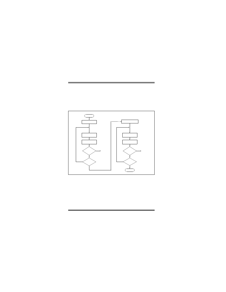
CONFIGURATION PROGRAMMING FLOW
4-bit
Command
Data Payload
Core Instruction
Step 1: Direct access to configuration memory.
0000
0000
8E A6
8C A6
BSF EECON1, EEPGD
BSF EECON1, CFGS
Step 2: Position the program counter.
(1)
0000
0000
EF 00
F8 00
GOTO 0x100000
Step 3: Set Table Pointer for configuration word to be written. Write even/odd addresses.
0000
0000
0000
0000
0000
0000
1111
0000
0000
1111
0000
0E 30
6E F8
0E 00
6E F7
0E 00
6E F6
<LSB><MSB ignored>
00 00
2A F6
<LSB ignored><MSB>
00 00
MOVLW 30h
MOVWF TBLPTRU
MOVLW 00h
MOVWF TBLPRTH
MOVLW 00h
MOVWF TBLPTRL
Load 2 bytes and start programming
NOP - hold PGC high for time P9
INCF TBLPTRL
Load 2 bytes and start programming
NOP - hold PGC high for time P9
Note
1: If the code protection bits are programmed while the program counter resides in the same block, then the interaction of
code protection logic may prevent further table write. To avoid this situation, move the program counter outside the code
protection area (e.g.,
GOTO 0x100000
).
2: Enabling the write protection of configuration bits (WRTC = 0 in CONFIG6H) will prevent further writing of configuration
bits. Always write all the configuration bits before enabling the write protection for configuration bits.
Load Even
Configuration
Start
Program
Program
MSB
Done
Delay P9 Time
for Write
Delay P9 Time
for Write
LSB
Load Odd
Configuration
Address
Address
Done
Start
PIC18FX220/X320
DS39592B-page 20
Preliminary
2002 Microchip Technology Inc.
4.0
READING THE DEVICE
4.1
Read Data EEPROM Memory
Data EEPROM is accessed one byte at a time via an
address pointer, EEADR, and a data latch, EEDATA.
Data EEPROM is read by loading EEADR with the
desired memory location and initiating a memory read
by appropriately configuring the EECON1 register. The
data will be loaded into EEDATA, where it may be seri-
ally output on PGD via the 4-bit command
0010
(shift
out data holding register). A delay of P6 must be intro-
duced after the falling edge of the 8th PGC of the oper-
and to allow PGD to transition from an input to an
output. During this time, PGC must be held low (see
Figure 4-2).
The command sequence to read a single byte of data
is shown in Table 4-1.
FIGURE 4-1:
READ DATA EEPROM
FLOW
TABLE 4-1:
READ DATA EEPROM MEMORY
FIGURE 4-2:
SHIFT OUT DATA HOLDING REGISTER TIMING (
0010
)
Start
Set
Address
Read
Byte
Done
No
Yes
Done?
Move to TABLAT
Shift Out Data
4-bit
Command
Data Payload
Core Instruction
Step 1: Direct access to data EEPROM.
0000
0000
9E A6
9C A6
BCF EECON1, EEPGD
BCF EECON1, CFGS
Step 2: Set the data EEPROM address pointer.
0000
0000
0E <Addr>
6E A9
MOVLW <Addr>
MOVWF EEADR
Step 3: Initiate a memory read.
0000
80 A6
BSF EECON1, RD
Step 4: Load data into the serial data holding register.
0000
0000
0010
50 A8
6E F5
<LSB><MSB>
MOVF EEDATA, W, 0
MOVWF TABLAT
Shift Out Data
(1)
Note
1:
The <LSB> is undefined. The <MSB> is the data.
1
2
3
4
PGC
P5
PGD
PGD = Input
Shift Data Out
P6
PGD = Output
5
6
7
8
1
2
3
4
P5a
9
10
11
13
15 16
14
12
Fetch Next 4-bit Command
0
1
0
0
PGD = Input
LSb
MSb
1
2
3
4
5
6
1
2
3
4
n
n
n
n
P14
2002 Microchip Technology Inc.
Preliminary
DS39592B-page 21
PIC18FX220/X320
4.2
Read Code Memory, ID Locations,
and Configuration Bits
Code memory is accessed one byte at a time, via the
4-bit command
1001
(Table Read, post increment).
The contents of memory pointed to by the Table Pointer
(TBLPTRU:TBLPTRH:TBLPTRL) are loaded into the
Table Latch and then serially output on PGD.
The 4-bit command is shifted in LSb first. The Read is
executed during the next 8 clocks, then shifted out on
PGD during the last 8 clocks, LSb to MSb. A delay of
P6 must be introduced after the falling edge of the 8th
PGC of the operand to allow PGD to transition from an
input to an output. During this time, PGC must be held
low (see Table 4-2). This operation also increments the
Table Pointer by one, pointing to the next byte in code
memory for the next read.
This technique will work to read any memory in the
000000h to 3FFFFFh address space, so it also applies
to the reading of the ID and configuration registers.
TABLE 4-2:
READ CODE MEMORY SEQUENCE
FIGURE 4-3:
TABLE READ POST INCREMENT INSTRUCTION TIMING (
1001
)
4-bit
Command
Data Payload
Core Instruction
Step 1: Set Table Pointer.
0000
0000
0000
0000
0000
0000
0E <Addr[21:16]>
6E F8
0E <Addr[15:8]>
6E F7
0E <Addr[7:0]>
6E F6
MOVLW Addr[21:16]
MOVWF TBLPTRU
MOVLW <Addr[15:8]>
MOVWF TBLPTRH
MOVLW <Addr[7:0]>
MOVWF TBLPTRL
Step 2: Read memory into Table Latch and then shift out on PGD, LSb to MSb.
1001
00 00
TBLRD *+
1
2
3
4
PGC
P5
PGD
PGD = Input
Shift Data Out
P6
PGD = Output
5
6
7
8
1
2
3
4
P5a
9
10
11
13
15
16
14
12
Fetch Next 4-bit Command
1
0
0
1
PGD = Input
LSb
MSb
1
2
3
4
5
6
1
2
3
4
n
n
n
n
P14
PIC18FX220/X320
DS39592B-page 22
Preliminary
2002 Microchip Technology Inc.
4.3
Verify Code Memory and ID
locations
The verify step involves reading back the code memory
space and comparing against the copy held in the pro-
grammer’s buffer. Memory reads occur a single byte at
a time, so two bytes must be read to compare against
the word in the programmer’s buffer. Refer to
Section 4.2 for implementation details of reading code
memory.
The Table Pointer must be manually set to 200000h
(base address of the ID locations). The post-increment
feature of the Table Read 4-bit command may not be
used to increment the Table Pointer to 200000h. The
post-increment feature may then be used to increment
to 200001h, 200002h
…
.
FIGURE 4-4:
VERIFY CODE MEMORY FLOW
4.4
Verify Configuration Bits
A configuration address may be read and output on
PGD via the 4-bit command
1001
. Configuration data
is read and written in a byte-wise fashion, so it is not
necessary to merge two bytes into a word prior to a
compare. The result may then be immediately com-
pared to the appropriate configuration data in the pro-
grammer’s memory for verification. Refer to
Section 4.2 for implementation details of reading
configuration data.
4.5
Verify Data EEPROM
A data EEPROM address may be read via a sequence
of core instructions (4-bit command
0000
) and then
output on PGD via the 4-bit command
0010
(shift out
data holding register). The result may then be immedi-
ately compared to the appropriate data in the program-
mer’s memory for verification. Refer to Section 4.1 for
implementation details of reading data EEPROM.
Read Low Byte
Read High byte
Does
word = expect
data?
Failure,
Report
Error
All
code memory
verified?
No
Yes
No
Set Pointer = 0
Start
Set Pointer = 200000h
Yes
Read Low Byte
Read High byte
Does
word = expect
data?
Failure,
Report
Error
All
ID locations
verified?
No
Yes
Done
Yes
No
2002 Microchip Technology Inc.
Preliminary
DS39592B-page 23
PIC18FX220/X320
5.0
CONFIGURATION WORD
The devices have several configuration words. Bits in
these registers can be set or cleared to select various
device configurations. All other memory areas should
be programmed and verified prior to setting configura-
tion words. These bits may be read out normally even
after read or code protected. Tables 5-2, 5-3 and 5-4
provide information on various configuration bits.
5.1
ID Locations
A user may store identification information (ID) in eight
ID locations mapped in 200000h:200007h. It is recom-
mended that the most significant nibble of each ID be
0Fh. In doing so, if the user code inadvertently tries to
execute from the ID space, the ID data will execute as
NOP
.
5.2
Device ID Word
The device ID word for the devices is located at
3FFFFEh:3FFFFFh. These bits may be used by the
programmer to identify what device type is being pro-
grammed and read out normally, even after code or
read protected.
5.3
Low Voltage Programming (LVP) Bit
The LVP bit in configuration register CONFIG4L
enables low voltage ICSP programming. The LVP bit
defaults to a ‘1’ following an erase.
If Low Voltage Programming mode is not used, the LVP
bit can be programmed to a ‘0’ and RB5/PGM becomes
a digital I/O pin. However, the LVP bit may only be pro-
grammed by entering the high voltage ICSP mode,
where MCLR/V
PP
is raised to V
IHH
. Once the LVP bit is
programmed to a ‘0’, only the high voltage ICSP mode
is available and only the high voltage ICSP mode can
be used to program the device.
TABLE 5-1:
DEVICE ID VALUE
Note 1: The normal high voltage ICSP mode is
always available, regardless of the state
of the LVP bit, by applying V
IHH
to the
MCLR/V
PP
pin.
2: While in Low Voltage ICSP mode, the
RB5 pin can no longer be used as a
general purpose I/O.
Device
Device ID Value
DEVID2
DEVID1
PIC18F1220
07
111x xxxx
PIC18F2220
05
100x xxxx
PIC18F4220
05
101x xxxx
PIC18F1320
07
110x xxxx
PIC18F2320
05
000x xxxx
PIC18F4320
05
001x xxxx
PIC18FX220/X320
DS39592B-page 24
Preliminary
2002 Microchip Technology Inc.
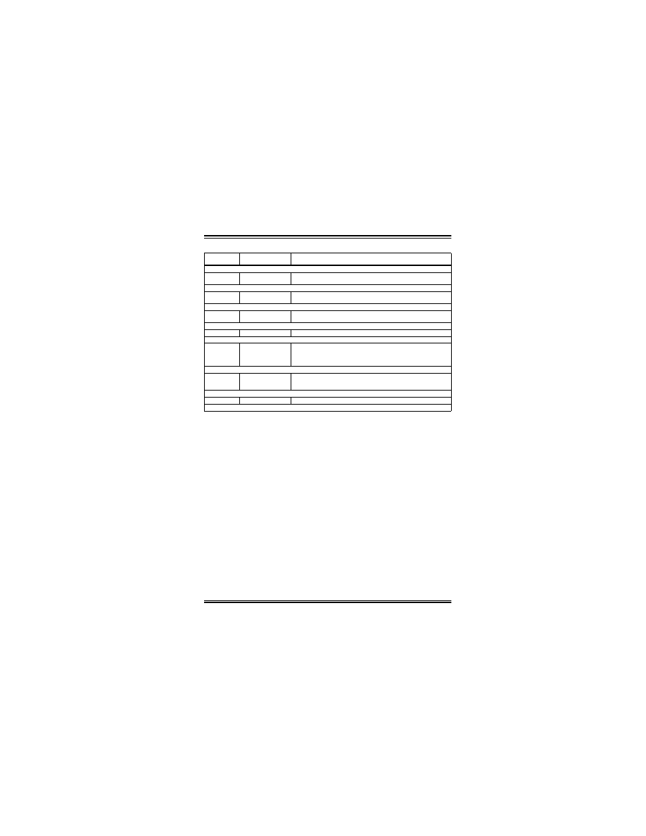
TABLE 5-2:
PIC18F2X20/PIC18F4X20 CONFIGURATION BITS AND DEVICE IDs
TABLE 5-3:
PIC18F1X20 CONFIGURATION BITS AND DEVICE IDs
File Name
Bit 7
Bit 6
Bit 5
Bit 4
Bit 3
Bit 2
Bit 1
Bit 0
Erased or
“Blank” Value
300000h CONFIG1L
—
—
—
—
—
—
—
—
0000 0000
300001h CONFIG1H
IESO
FCMEM
—
—
FOSC3
FOSC2
FOSC1
FOSC0
1100 1111
300002h CONFIG2L
—
—
—
—
BORV1
BORV0
BOREN
PWRTEN
0000 1111
300003h CONFIG2H
—
—
—
WDPS3
WDPS2
WDPS1
WDPS0
WDTEN
0001 1111
300004h CONFIG3L
—
—
—
—
—
—
—
—
0000 0000
300005h CONFIG3H
MCLRE
—
—
—
—
—
PBADEN
CCP2MX
1000 0011
300006h CONFIG4L
DEBUG
—
—
—
—
LVP
—
STVREN
1000 0101
300007h CONFIG4H
—
—
—
—
—
—
—
—
0000 0000
300008h CONFIG5L
—
—
—
—
CP3
CP2
CP1
CP0
0000 1111
300009h CONFIG5H
CPD
CPB
—
—
—
—
—
—
1100 0000
30000Ah CONFIG6L
—
—
—
—
WRT3
WRT2
WRT1
WRT0
0000 1111
30000Bh CONFIG6H
WRTD
WRTB
WRTC
—
—
—
—
—
1110 0000
30000Ch CONFIG7L
—
—
—
—
EBTR3
EBTR2
EBTR1
EBTR0
0000 1111
30000Dh CONFIG7H
—
EBTRB
—
—
—
—
—
—
0100 0000
3FFFFEh DEVID1
DEV2
DEV1
DEV0
REV4
REV3
REV2
REV1
REV0
3FFFFFh DEVID2
DEV10
DEV9
DEV8
DEV7
DEV6
DEV5
DEV4
DEV3
File Name
Bit 7
Bit 6
Bit 5
Bit 4
Bit 3
Bit 2
Bit 1
Bit 0
Erased or
“Blank” Value
300000h CONFIG1L
—
—
—
—
—
—
—
—
0000 0000
300001h CONFIG1H
IESO
FCMEM
—
—
FOSC3
FOSC2
FOSC1
FOSC0
1100 1111
300002h CONFIG2L
—
—
—
—
BORV1
BORV0
BOREN
PWRTEN
0000 1111
300003h CONFIG2H
—
—
—
WDPS3
WDPS2
WDPS1
WDPS0
WDTEN
0001 1111
300004h CONFIG3L
—
—
—
—
—
—
—
—
0000 0000
300005h CONFIG3H
MCLRE
—
—
—
—
—
—
—
1000 0000
300006h CONFIG4L
DEBUG
—
—
—
—
LVP
—
STVREN
1000 0101
300007h CONFIG4H
—
—
—
—
—
—
—
—
0000 0000
300008h CONFIG5L
—
—
—
—
—
—
CP1
CP0
0000 0011
300009h CONFIG5H
CPD
CPB
—
—
—
—
—
—
1100 0000
30000Ah CONFIG6L
—
—
—
—
—
—
WRT1
WRT0
0000 0011
30000Bh CONFIG6H
WRTD
WRTB
WRTC
—
—
—
—
—
1110 0000
30000Ch CONFIG7L
—
—
—
—
—
—
EBTR1
EBTR0
0000 0011
30000Dh CONFIG7H
—
EBTRB
—
—
—
—
—
—
0100 0000
3FFFFEh DEVID1
DEV2
DEV1
DEV0
REV4
REV3
REV2
REV1
REV0
3FFFFFh DEVID2
DEV10
DEV9
DEV8
DEV7
DEV6
DEV5
DEV4
DEV3

2002 Microchip Technology Inc.
Preliminary
DS39592B-page 25
PIC18FX220/X320
TABLE 5-4:
PIC18FX220/X320 BIT DESCRIPTION
Bit Name
Configuration
Words
Description
IESO
CONFIG1H
Internal External Switch Over bit
1
= Internal External Switch Over mode enabled
0
= Internal External Switch Over mode disabled
FCMEN
CONFIG1H
Fail-Safe Clock Monitor Enable bit
1
= Fail-Safe Clock Monitor enabled
0
= Fail-Safe Clock Monitor disabled
FOSC3:FOSC0
CONFIG1H
Oscillator Selection bits
11xx
= External RC oscillator, CLKO function on RA6
101x
= External RC oscillator, CLKO function on RA6
1001
= Internal RC oscillator, CLKO function on RA6, port function on RA7
1000
= Internal RC oscillator, port function on RA6, port function on RA7
0111
= External RC oscillator, port function on RA6
0110
= HS oscillator, PLL enabled (clock frequency = 4 x FOSC1)
0101
= EC oscillator, port function on RA6
0100
= EC oscillator, CLKO function on RA6
0011
= External RC oscillator, CLKO function on RA6
0010
= HS oscillator
0001
= XT oscillator
0000
= LP oscillator
BORV1:BORV0
CONFIG2L
Brown-out Reset Voltage bits
11
= V
BOR
set to 2.0V
10
= V
BOR
set to 2.7V
01
= V
BOR
set to 4.2V
00
= V
BOR
set to 4.5V
BOREN
CONFIG2L
Brown-out Reset Enable bit
1
= Brown-out Reset enabled
0
= Brown-out Reset disabled
PWRTEN
CONFIG2L
Power-up Timer Enable bit
1
= PWRT disabled
0
= PWRT enabled
WDPS3:WDPS0
CONFIG2H
Watchdog Timer Postscaler Select bits
1111
= 1:32,768
1110
= 1:16,384
1101
= 1:8,192
1100
= 1:4,096
1011
= 1:2,048
1010
= 1:1,024
1001
= 1:512
1000
= 1:256
0111
= 1:128
0110
= 1:64
0101
= 1:32
0100
= 1:16
0011
= 1:8
0010
= 1:4
0001
= 1:2
0000
= 1:1
WDTEN
CONFIG2H
Watchdog Timer Enable bit
1
= WDT enabled
0
= WDT disabled (control is placed on SWDTEN bit)
PIC18FX220/X320
DS39592B-page 26
Preliminary
2002 Microchip Technology Inc.
MCLRE
CONFIG3H
MCLR Pin Enable bit for PIC18F2X20, PIC18F4X20
1
= MCLR pin enabled, RE3 input pin disabled
0
= RE3 input pin enabled, MCLR pin disabled
MCLRE
CONFIG3H
MCLR Pin Enable bit for PIC18F1X20
1
= MCLR pin enabled, RA5 input pin disabled
0
= RA5 input pin enabled, MCLR pin disabled
PBADEN
CONFIG3H
PORTB A/D Enable bit
1
= PORTB A/D<4:0> pins are configured as analog input channels on RESET
0
= PORTB A/D<4:0> pins are configured as digital I/O on RESET
CCP2MX
CONFIG3H
CCP2 MUX bit
1
= CCP2 input/output is multiplexed with RC1
0
= CCP2 input/output is multiplexed with RB3
DEBUG
CONFIG4L
In-Circuit Debugger Enable bit
1
= In-Circuit debugger disabled (RB6, RB7 have I/O port function)
0
= In-Circuit debugger enabled (RB6, RB7 have ICSP serial
communication function)
LVP
CONFIG4L
Low Voltage Programming Enable bit
1
= Low Voltage Programming enabled, RB5 is the PGM pin
0
= Low Voltage Programming disabled, RB5 is an I/O pin
STVREN
CONFIG4L
Stack Overflow/Underflow Reset Enable bit
1
= RESET on Stack Overflow/Underflow enabled
0
= RESET on Stack Overflow/Underflow disabled
CP3
CONFIG5L
Code Protection bits (Block 3 code memory area: 001800h - 001FFFh)
for PIC18F2X20/PIC18F4X20
1
= Block 3 is not code protected
0
= Block 3 is code protected
CP2
CONFIG5L
Code Protection bits (Block 2 code memory area: 001000h - 0017FFh)
for PIC18F2X20/PIC18F4X20
1
= Block 2 is not code protected
0
= Block 2 is code protected
CP1
CONFIG5L
Code Protection bits (Block 1 code memory area: 000800h - 000FFFh)
for PIC18F1220
1
= Block 1 is not code protected
0
= Block 1 is code protected
CP1
CONFIG5L
Code Protection bits (Block 1 code memory area: 001000h - 001FFFh)
for PIC18F1320
1
= Block 1 is not code protected
0
= Block 1 is code protected
CP1
CONFIG5L
Code Protection bits (Block 1 code memory area: 000800h - 000FFFh)
for PIC18F2X20/PIC18F4X20
1
= Block 1 is not code protected
0
= Block 1 is code protected
CP0
CONFIG5L
Code Protection bits (Block 0 code memory area: 000200h - 0007FFh)
for PIC18F1220
1
= Block 0 is not code protected
0
= Block 0 is code protected
TABLE 5-4:
PIC18FX220/X320 BIT DESCRIPTION (CONTINUED)
Bit Name
Configuration
Words
Description

2002 Microchip Technology Inc.
Preliminary
DS39592B-page 27
PIC18FX220/X320
CP0
CONFIG5L
Code Protection bits (Block 0 code memory area: 000200h - 000FFFh)
for PIC18F1320
1
= Block 0 is not code protected
0
= Block 0 is code protected
CP0
CONFIG5L
Code Protection bits (Block 0 code memory area: 000200h - 0007FFh)
for PIC18F2X20/PIC18F4X20
1
= Block 0 is not code protected
0
= Block 0 is code protected
CPD
CONFIG5H
Code Protection bits (Data EEPROM)
1
= Data EEPROM is not code protected
0
= Data EEPROM is code protected
CPB
CONFIG5H
Code Protection bits (Boot block memory area: 000000h - 0001FFh)
1
= Boot block is not code protected
0
= Boot block is code protected
WRT3
CONFIG6L
Write Protection bits (Block 3 code memory area: 001800h - 001FFFh)
for PIC18F2X20/PIC18F4X20
1
= Block 3 is not write protected
0
= Block 3 is write protected
WRT2
CONFIG6L
Write Protection bits (Block 2 code memory area: 001000h - 0017FFh)
for PIC18F2X20/PIC18F4X20
1
= Block 2 is not write protected
0
= Block 2 is write protected
WRT1
CONFIG6L
Write Protection bits (Block 1 code memory area: 000800h - 000FFFh)
for PIC18F1220
1
= Block 1 is not write protected
0
= Block 1 is write protected
WRT1
CONFIG6L
Write Protection bits (Block 1 code memory area: 001000h - 001FFFh)
for PIC18F1320
1
= Block 1 is not write protected
0
= Block 1 is write protected
WRT1
CONFIG6L
Write Protection bits (Block 1 code memory area: 000800h - 000FFFh)
for PIC18F2X20/PIC18F4X20
1
= Block 1 is not write protected
0
= Block 1 is write protected
WRT0
CONFIG6L
Write Protection bits (Block 0 code memory area: 000200h - 0007FFh)
for PIC18F1220
1
= Block 0 is not write protected
0
= Block 0 is write protected
WRT0
CONFIG6L
Write Protection bits (Block 0 code memory area: 000200h - 000FFFh)
for PIC18F1320
1
= Block 0 is not write protected
0
= Block 0 is write protected
WRT0
CONFIG6L
Write Protection bits (Block 0 code memory area: 000200h - 0007FFh)
for PIC18F2X20/PIC18F4X20
1
= Block 0 is not write protected
0
= Block 0 is write protected
WRTD
CONFIG6H
Write Protection bit (Data EEPROM)
1
= Data EEPROM is not write protected
0
= Data EEPROM is write protected
TABLE 5-4:
PIC18FX220/X320 BIT DESCRIPTION (CONTINUED)
Bit Name
Configuration
Words
Description

PIC18FX220/X320
DS39592B-page 28
Preliminary
2002 Microchip Technology Inc.
WRTB
CONFIG6H
Write Protection bit (Boot block memory area: 000000h - 0001FFh)
1
= Boot block is not write protected
0
= Boot block is write protected
WRTC
CONFIG6H
Write Protection bit (Configuration Registers: 300000h - 3000FFh)
1
= Configuration Registers are not write protected
0
= Configuration Registers are write protected
EBTR3
CONFIG7L
Table Read Protection bit (Block 3 code memory area: 001800h - 001FFFh)
for PIC18F2X20/PIC18F4X20
1
= Block 3 is not protected from table reads executed in other blocks
0
= Block 3 is protected from table reads executed in other blocks
EBTR2
CONFIG7L
Table Read Protection bit (Block 2 code memory area: 001000h - 0017FFh)
for PIC18F2X20/PIC18F4X20
1
= Block 2 is not protected from table reads executed in other blocks
0
= Block 2 is protected from table reads executed in other blocks
EBTR1
CONFIG7L
Table Read Protection bit (Block 1 code memory area: 000800h - 000FFFh)
for PIC18F1220
1
= Block 1 is not protected from table reads executed in other blocks
0
= Block 1 is protected from table reads executed in other blocks
EBTR1
CONFIG7L
Table Read Protection bit (Block 1 code memory area: 001000h - 001FFFh)
for PIC18F1320
1
= Block 1 is not protected from table reads executed in other blocks
0
= Block 1 is protected from table reads executed in other blocks
EBTR1
CONFIG7L
Table Read Protection bit (Block 1 code memory area: 000800h - 000FFFh)
for PIC18F2X20/PIC18F4X20
1
= Block 1 is not protected from table reads executed in other blocks
0
= Block 1 is protected from table reads executed in other blocks
EBTR0
CONFIG7L
Table Read Protection bit (Block 0 code memory area: 000200h - 0007FFh)
for PIC18F1220
1
= Block 0 is not protected from table reads executed in other blocks
0
= Block 0 is protected from table reads executed in other blocks
EBTR0
CONFIG7L
Table Read Protection bit (Block 0 code memory area: 000200h - 000FFFh)
for PIC18F1320
1
= Block 0 is not protected from table reads executed in other blocks
0
= Block 0 is protected from table reads executed in other blocks
EBTR0
CONFIG7L
Table Read Protection bit (Block 0 code memory area: 000200h - 0007FFh)
for PIC18F2X20/PIC18F4X20
1
= Block 0 is not protected from table reads executed in other blocks
0
= Block 0 is protected from table reads executed in other blocks
EBTRB
CONFIG7H
Table Read Protection bit (Boot block memory area: 000000h - 0001FFh)
1
= Boot block is not protected from table reads executed in other blocks
0
= Boot block is protected from table reads executed in other blocks
DEV10:DEV3
DEVID2
Device ID bits
These bits are used with the DEV2:DEV0 bits in the DEVID1 register to
identify part number.
DEV2:DEV0
DEVID1
Device ID bits
These bits are used with the DEV10:DEV3 bits in the DEVID2 register to
identify part number.
REV4:REV0
DEVID1
Revision ID bits
These bits are used to indicate the revision of the device.
TABLE 5-4:
PIC18FX220/X320 BIT DESCRIPTION (CONTINUED)
Bit Name
Configuration
Words
Description
2002 Microchip Technology Inc.
Preliminary
DS39592B-page 29
PIC18FX220/X320
5.4
Embedding Configuration Word
Information in the HEX File
To allow portability of code, a device programmer is
required to read the configuration word locations from
the HEX file. If configuration word information is not
present in the HEX file, then a simple warning message
should be issued. Similarly, while saving a HEX file, all
configuration word information must be included. An
option to not include the configuration word information
may be provided. When embedding configuration word
information in the HEX file, it should start at address
300000h.
Microchip Technology Inc. feels strongly that this
feature is important for the benefit of the end customer.
5.5
Embedding Data EEPROM
Information in the HEX File
To allow portability of code, a device programmer is
required to read the data EEPROM information from
the HEX file. If data EEPROM information is not
present, a simple warning message should be issued.
Similarly, when saving a HEX file, all data EEPROM
information must be included. An option to not include
the data EEPROM information may be provided. When
embedding data EEPROM information in the HEX file,
it should start at address F00000h.
Microchip Technology Inc. believes that this feature is
important for the benefit of the end customer.
5.6
Checksum Computation
The checksum is calculated by summing the following:
• The contents of all code memory locations
• The configuration word, appropriately masked
• ID locations
The Least Significant 16-bits of this sum are the
checksum.
Table 5-7 describes how to calculate the checksum for
each device.
TABLE 5-5:
CHECKSUM COMPUTATION - PIC18F1320
Note:
The checksum calculation differs depend-
ing on the code protect setting. Since the
code memory locations read out differently
depending on the code protect setting, the
table describes how to manipulate the
actual code memory values to simulate the
values that would be read from a protected
device. When calculating a checksum by
reading a device, the entire code memory
can simply be read and summed. The con-
figuration word and ID locations can
always be read.
Device
Code
Protect
Checksum
Blank
Value
0xAA at 0
and Max
Address
PIC18F1320
None
SUM (0000:01FFh) + SUM (0200:07FFh) + SUM (0800:0FFFh) +
(CONFIG1H & 0CFh) + (CONFIG2L & 0Fh) + (CONFIG2H & 1Fh) +
(CONFIG3H & 080h) + (CONFIG4L & 085h) + (CONFIG5L & 03h) +
(CONFIG5H & 0C0h) + (CONFIG6L & 03h) + (CONFIG6H & 0E0h) +
(CONFIG7L & 03h) + (CONFIG7H & 040h)
E3EB
E341
Boot Block SUM (0200:07FFh) + SUM (0800:0FFFh) + (CONFIG1H & 0CFh) +
(CONFIG2L & 0Fh) + (CONFIG2H & 1Fh) + (CONFIG3H & 080h) +
(CONFIG4L & 085h) + (CONFIG5L & 03h) + (CONFIG5H & 0C0h) +
(CONFIG6L & 03h) + (CONFIG6H & 0E0h) + (CONFIG7L & 03h) +
(CONFIG7H & 040h) + SUM (IDs)
E5D5
E56C
Boot/
Panel1/
Panel2
(CONFIG1H & 0CFh) + (CONFIG2L & 0Fh) + (CONFIG2H & 1Fh) +
(CONFIG3H & 080h) + (CONFIG4L & 085h) + (CONFIG5L & 03h) +
(CONFIG5H & 0C0h) + (CONFIG6L & 03h) + (CONFIG6H & 0E0h) +
(CONFIG7L & 03h) + (CONFIG7H & 040h) + SUM (IDs)
03D2
03BE
All
(CONFIG1H & 0CFh) + (CONFIG2L & 0Fh) + (CONFIG2H & 1Fh) +
(CONFIG3H & 083h) + (CONFIG4L & 085h) + (CONFIG5L & 0Fh) +
(CONFIG5H & 0C0h) + (CONFIG6L & 0Fh) + (CONFIG6H & 0E0h) +
(CONFIG7L & 0Fh) + (CONFIG7H & 040h) + SUM (IDs)
03D2
03BE
Legend:
Item
Description
CONFIG
=
Configuration Word
SUM[a:b]
=
Sum of locations, a to b inclusive
SUM (IDs) =
Byte-wise sum of lower four bits of all ID locations
+
=
Addition
&
=
Bit-wise AND
PIC18FX220/X320
DS39592B-page 30
Preliminary
2002 Microchip Technology Inc.
TABLE 5-6:
CHECKSUM COMPUTATION - PIC18F1220
Device
Code
Protect
Checksum
Blank
Value
0xAA at 0
and Max
Address
PIC18F1220
None
SUM (0000:01FFh) + SUM (0200:0FFFh) + SUM (1000:1FFFh) +
(CONFIG1H & 0CFh) + (CONFIG2L & 0Fh) + (CONFIG2H & 1Fh) +
(CONFIG3H & 080h) + (CONFIG4L & 085h) + (CONFIG5L & 03h) +
(CONFIG5H & 0C0h) + (CONFIG6L & 03h) + (CONFIG6H & 0E0h) +
(CONFIG7L & 03h) + (CONFIG7H & 040h)
F3EB
F341
Boot Block SUM (0200:0FFFh) + SUM (1000:1FFFh) + (CONFIG1H & 0CFh) +
(CONFIG2L & 0Fh) + (CONFIG2H & 1Fh) + (CONFIG3H & 080h) +
(CONFIG4L & 085h) + (CONFIG5L & 03h) + (CONFIG5H & 0C0h) +
(CONFIG6L & 03h) + (CONFIG6H & 0E0h) + (CONFIG7L & 03h) +
(CONFIG7H & 040h) + SUM (IDs)
F5D6
F56D
Boot/
Panel1/
Panel2
(CONFIG1H & 0CFh) + (CONFIG2L & 0Fh) + (CONFIG2H & 1Fh) +
(CONFIG3H & 080h) + (CONFIG4L & 085h) + (CONFIG5L & 03h) +
(CONFIG5H & 0C0h) + (CONFIG6L & 03h) + (CONFIG6H & 0E0h) +
(CONFIG7L & 03h) + (CONFIG7H & 040h) + SUM (IDs)
03D3
03BF
All
(CONFIG1H & 0CFh) + (CONFIG2L & 0Fh) + (CONFIG2H & 1Fh) +
(CONFIG3H & 080h) + (CONFIG4L & 085h) + (CONFIG5L & 03h) +
(CONFIG5H & 0C0h) + (CONFIG6L & 03h) + (CONFIG6H & 0E0h) +
(CONFIG7L & 03h) + (CONFIG7H & 040h) + SUM (IDs)
03D3
03BF
Legend:
Item
Description
CONFIG
=
Configuration Word
SUM[a:b]
=
Sum of locations, a to b inclusive
SUM (IDs) =
Byte-wise sum of lower four bits of all ID locations
+
=
Addition
&
=
Bit-wise AND

2002 Microchip Technology Inc.
Preliminary
DS39592B-page 31
PIC18FX220/X320
TABLE 5-7:
CHECKSUM COMPUTATION - PIC18F2X20/PIC18F4X20
Device
Code
Protect
Checksum
Blank
Value
0xAA at 0
and Max
Address
PIC18F2320/
PIC18F4320
None
SUM (0000:01FFh) + SUM (0200:07FFh) + SUM (0800:0FFFh) +
SUM (1000:17FFh) + SUM (1800:1FFFh) + (CONFIG1H & 0CFh) +
(CONFIG2L & 0Fh) + (CONFIG2H & 1Fh) + (CONFIG3H & 083h) + (CONFIG4L
& 085h) + (CONFIG5L & 0Fh) + (CONFIG5H & 0C0h) + (CONFIG6L & 0Fh) +
(CONFIG6H & 0E0h) + (CONFIG7L & 0Fh) + (CONFIG7H & 040h)
0E412h
0E368h
Boot Block SUM (0200:07FFh) + SUM (0800:0FFFh) + SUM (1000:17FFh) +
SUM (1800:1FFFh) + (CONFIG1H & 0CFh) + (CONFIG2L & 0Fh) +
(CONFIG2H & 1Fh) + (CONFIG3H & 083h) + (CONFIG4L & 085h) +
(CONFIG5L & 0Fh) + (CONFIG5H & 0C0h) + (CONFIG6L & 0Fh) +
(CONFIG6H & 0E0h) + (CONFIG7L & 0Fh) + (CONFIG7H & 040h) +
SUM (IDs)
0E5E7h
0E59Ch
Boot Block/
Block 0
SUM (0800:0FFFh) + SUM (1000:17FFh) + SUM (1800:1FFFh) +
(CONFIG1H & 0CFh) + (CONFIG2L & 0Fh) + (CONFIG2H & 1Fh) +
(CONFIG3H & 083h) + (CONFIG4L & 085h) + (CONFIG5L & 0Fh) +
(CONFIG5H & 0C0h) + (CONFIG6L & 0Fh) + (CONFIG6H & 0E0h) +
(CONFIG7L & 0Fh) + (CONFIG7H & 040h) + SUM (IDs)
0EBE6h
0EB9Bh
Boot Block/
Block 0/
Block 1
SUM (1000:17FFh) + SUM (1800:1FFFh) + (CONFIG1H & 0CFh) +
(CONFIG2L & 0Fh) + (CONFIG2H & 1Fh) + (CONFIG3H & 083h) + (CONFIG4L
& 085h) + (CONFIG5L & 0Fh) + (CONFIG5H & 0C0h) + (CONFIG6L & 0Fh) +
(CONFIG6H & 0E0h) + (CONFIG7L & 0Fh) + (CONFIG7H & 040h) + SUM (IDs)
0F3E4h
0F399h
Boot Block/
Block 0/
Block 1/
Block 2
SUM (1800:1FFFh) + (CONFIG1H & 0CFh) + (CONFIG2L & 0Fh) +
(CONFIG2H & 1Fh) + (CONFIG3H & 083h) + (CONFIG4L & 085h) +
(CONFIG5L & 0Fh) + (CONFIG5H & 0C0h) + (CONFIG6L & 0Fh) +
(CONFIG6H & 0E0h) + (CONFIG7L & 0Fh) + (CONFIG7H & 040h) +
SUM (IDs)
0FBE0h
0FB95h
Boot Block/
Block 0/
Block 1/
Block 2/
Block 3
(CONFIG1H & 0CFh) + (CONFIG2L & 0Fh) + (CONFIG2H & 1Fh) +
(CONFIG3H & 083h) + (CONFIG4L & 085h) + (CONFIG5L & 0Fh) +
(CONFIG5H & 0C0h) + (CONFIG6L & 0Fh) + (CONFIG6H & 0E0h) +
(CONFIG7L & 0Fh) + (CONFIG7H & 040h) + SUM (IDs)
03D8h
03E2h
All
(CONFIG1H & 0CFh) + (CONFIG2L & 0Fh) + (CONFIG2H & 1Fh) +
(CONFIG3H & 083h) + (CONFIG4L & 085h) + (CONFIG5L & 0Fh) +
(CONFIG5H & 0C0h) + (CONFIG6L & 0Fh) + (CONFIG6H & 0E0h) +
(CONFIG7L & 0Fh) + (CONFIG7H & 040h) + SUM (IDs)
03D8h
03E2h
Legend:
Item
Description
CONFIG
=
Configuration Word
SUM[a:b]
=
Sum of locations, a to b inclusive
SUM (IDs) =
Byte-wise sum of lower four bits of all ID locations
+
=
Addition
&
=
Bit-wise AND
PIC18FX220/X320
DS39592B-page 32
Preliminary
2002 Microchip Technology Inc.
Device
Code
Protect
Checksum
Blank
Value
0xAA at 0
and Max
Address
PIC18F2220/
PIC18F4220
None
SUM (0000:01FFh) + SUM (0200:07FFh) + SUM (0800:0FFFh) +
(CONFIG1H & 0CFh) + (CONFIG2L & 0Fh) + (CONFIG2H & 1Fh) +
(CONFIG3H & 083h) + (CONFIG4L & 085h) + (CONFIG5L & 0Fh) +
(CONFIG5H & 0C0h) + (CONFIG6L & 0Fh) + (CONFIG6H & 0E0h) +
(CONFIG7L & 0Fh) + (CONFIG7H & 040h)
0F412h
0F368h
Boot Block SUM (0200:07FFh) + SUM (0800:0FFFh) + (CONFIG1H & 0CFh) +
(CONFIG2L & 0Fh) + (CONFIG2H & 1Fh) + (CONFIG3H & 083h) + (CONFIG4L
& 085h) + (CONFIG5L & 0Fh) + (CONFIG5H & 0C0h) + (CONFIG6L & 0Fh) +
(CONFIG6H & 0E0h) + (CONFIG7L & 0Fh) + (CONFIG7H & 040h) + SUM (IDs)
0F5E8h
0F59Dh
Boot Block/
Block 0
SUM (0800:0FFFh) + (CONFIG1H & 0CFh) + (CONFIG2L & 0Fh) +
(CONFIG2H & 1Fh) + (CONFIG3H & 083h) + (CONFIG4L & 085h) +
(CONFIG5L & 0Fh) + (CONFIG5H & 0C0h) + (CONFIG6L & 0Fh) +
(CONFIG6H & 0E0h) + (CONFIG7L & 0Fh) + (CONFIG7H & 040h) + SUM (IDs)
0FBE7h
0FB9Ch
Boot Block/
Block 0/
Block 1
(CONFIG1H & 0CFh) + (CONFIG2L & 0Fh) + (CONFIG2H & 1Fh) +
(CONFIG3H & 083h) + (CONFIG4L & 085h) + (CONFIG5L & 0Fh) +
(CONFIG5H & 0C0h) + (CONFIG6L & 0Fh) + (CONFIG6H & 0E0h) +
(CONFIG7L & 0Fh) + (CONFIG7H & 040h) + SUM (IDs)
03E5h
03EFh
All
(CONFIG1H & 0CFh) + (CONFIG2L & 0Fh) + (CONFIG2H & 1Fh) +
(CONFIG3H & 083h) + (CONFIG4L & 085h) + (CONFIG5L & 0Fh) +
(CONFIG5H & 0C0h) + (CONFIG6L & 0Fh) + (CONFIG6H & 0E0h) +
(CONFIG7L & 0Fh) + (CONFIG7H & 040h) + SUM (IDs)
03E5h
03EFh
Legend:
Item
Description
CONFIG
=
Configuration Word
SUM[a:b]
=
Sum of locations, a to b inclusive
SUM (IDs) =
Byte-wise sum of lower four bits of all ID locations
+
=
Addition
&
=
Bit-wise AND
TABLE 5-7:
CHECKSUM COMPUTATION - PIC18F2X20/PIC18F4X20 (CONTINUED)
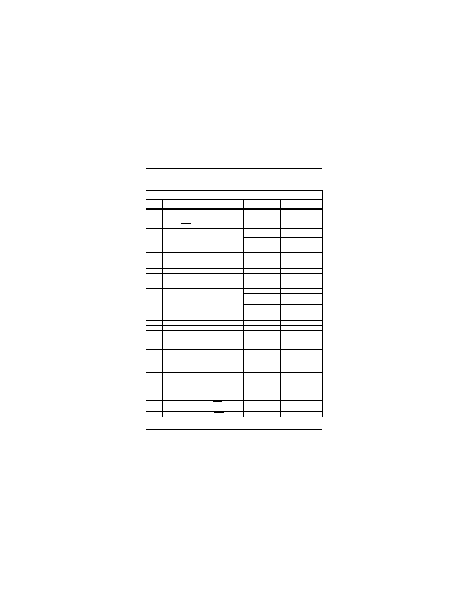
2002 Microchip Technology Inc.
Preliminary
DS39592B-page 33
PIC18FX220/X320
6.0
AC/DC CHARACTERISTICS
TABLE 6-1:
TIMING REQUIREMENTS FOR PROGRAM/VERIFY TEST MODE
Standard Operating Conditions
Operating Temperature: 25
°
C is recommended
Param
No.
Sym
Characteristic
Min
Max
Units
Conditions
D110
V
IHH
High Voltage Programming Voltage on
MCLR/V
PP
9.00
13.25
V
D110A
V
IHL
Low Voltage Programming Voltage on
MCLR/V
PP
2.00
5.50
V
D111
V
DD
Supply Voltage during Programming
2.00
5.50
V
Normal
programming
4.50
5.50
V
Bulk erase
operations
D112
I
PP
Programming Current on MCLR/V
PP
—
300
µ
A
D113
I
DDP
Supply Current during Programming
—
1
mA
D031
V
IL
Input Low Voltage
V
SS
0.2 V
SS
V
D041
V
IH
Input High Voltage
0.8 V
DD
V
DD
V
D080
V
OL
Output Low Voltage
—
0.6
V
I
OL
= 8.5 mA
D090
V
OH
Output High Voltage
V
DD
- 0.7
—
V
I
OH
= -3.0 mA
D012
C
IO
Capacitive Loading on I/O pin (PGD)
—
50
pF
To meet AC
specifications
P2
Tsclk
Serial Clock (Program Clock (PGC))
Period
100
—
ns
V
DD
= 5.0V
1
—
µ
s
V
DD
= 2.0V
P2A
TsclkL
Serial Clock (Program Clock (PGC))
Low Time
40
—
ns
V
DD
= 5.0V
400
—
ns
V
DD
= 2.0V
P2B
TsclkH
Serial Clock (Program Clock (PGC))
High Time
40
—
ns
V
DD
= 5.0V
400
—
ns
V
DD
= 2.0V
P3
Tset1
Input Data Setup Time to Serial Clock
↓
15
—
ns
P4
Thld1
Input Data Hold Time from SCLK
↓
15
—
ns
P5
Tdly1
Delay between 4-bit Command and
Command Operand
20
—
ns
P5A
Tdly1a
Delay between 4-bit Command
Operand and next 4-bit Command
20
—
ns
P6
Tdly2
Delay between last SCLK
↓
of
Command Byte to first SCLK
↑
of Read
of Data Word
20
—
ns
P9
Tdly5
SCLK High Time
(minimum programming time)
1
—
ms
P10
Tdly6
SCLK Low Time after Programming
(high voltage discharge time)
5
—
µ
s
P11
Tdly7
Delay to allow Self-timed Data Write or
Bulk Erase to occur
5
—
ms
P12
Thld2
Input Data Hold Time from
MCLR/V
PP
↑
2
—
µ
s
P13
Tset2
V
DD
↑
Setup Time to MCLR/V
PP
↑
100
—
ns
P14
Tvalid
Data Out Valid from SCLK
↑
10
—
ns
P15
Tset3
PGM
↑
Setup Time to MCLR/V
PP
↑
2
—
µ
s

PIC18FX220/X320
DS39592B-page 34
Preliminary
2002 Microchip Technology Inc.
NOTES:

2002 Microchip Technology Inc.
Preliminary
DS39592B - page 35
Information contained in this publication regarding device
applications and the like is intended through suggestion only
and may be superseded by updates. It is your responsibility to
ensure that your application meets with your specifications.
No representation or warranty is given and no liability is
assumed by Microchip Technology Incorporated with respect
to the accuracy or use of such information, or infringement of
patents or other intellectual property rights arising from such
use or otherwise. Use of Microchip’s products as critical com-
ponents in life support systems is not authorized except with
express written approval by Microchip. No licenses are con-
veyed, implicitly or otherwise, under any intellectual property
rights.
Trademarks
The Microchip name and logo, the Microchip logo, K
EE
L
OQ
,
MPLAB, PIC, PICmicro, PICSTART and PRO MATE are
registered trademarks of Microchip Technology Incorporated
in the U.S.A. and other countries.
FilterLab, micro
ID
, MXDEV, MXLAB, PICMASTER, SEEVAL
and The Embedded Control Solutions Company are
registered trademarks of Microchip Technology Incorporated
in the U.S.A.
dsPIC, dsPICDEM.net, ECONOMONITOR, FanSense,
FlexROM, fuzzyLAB, In-Circuit Serial Programming, ICSP,
ICEPIC, microPort, Migratable Memory, MPASM, MPLIB,
MPLINK, MPSIM, PICC, PICDEM, PICDEM.net, rfPIC, Select
Mode and Total Endurance are trademarks of Microchip
Technology Incorporated in the U.S.A. and other countries.
Serialized Quick Turn Programming (SQTP) is a service mark
of Microchip Technology Incorporated in the U.S.A.
All other trademarks mentioned herein are property of their
respective companies.
© 2002, Microchip Technology Incorporated, Printed in the
U.S.A., All Rights Reserved.
Printed on recycled paper.
Microchip received QS-9000 quality system
certification for its worldwide headquarters,
design and wafer fabrication facilities in
Chandler and Tempe, Arizona in July 1999
and Mountain View, California in March 2002.
The Company’s quality system processes and
procedures are QS-9000 compliant for its
PICmicro
®
8-bit MCUs, K
EE
L
OQ
®
code hopping
devices, Serial EEPROMs, microperipherals,
non-volatile memory and analog products. In
addition, Microchip’s quality system for the
design and manufacture of development
systems is ISO 9001 certified.
Note the following details of the code protection feature on PICmicro
®
MCUs.
•
The PICmicro family meets the specifications contained in the Microchip Data Sheet.
•
Microchip believes that its family of PICmicro microcontrollers is one of the most secure products of its kind on the market today,
when used in the intended manner and under normal conditions.
•
There are dishonest and possibly illegal methods used to breach the code protection feature. All of these methods, to our knowl-
edge, require using the PICmicro microcontroller in a manner outside the operating specifications contained in the data sheet.
The person doing so may be engaged in theft of intellectual property.
•
Microchip is willing to work with the customer who is concerned about the integrity of their code.
•
Neither Microchip nor any other semiconductor manufacturer can guarantee the security of their code. Code protection does not
mean that we are guaranteeing the product as “unbreakable”.
•
Code protection is constantly evolving. We at Microchip are committed to continuously improving the code protection features of
our product.
If you have any further questions about this matter, please contact the local sales office nearest to you.

DS39592B-page 36
Preliminary
2002 Microchip Technology Inc.
M
AMERICAS
Corporate Office
2355 West Chandler Blvd.
Chandler, AZ 85224-6199
Tel: 480-792-7200 Fax: 480-792-7277
Technical Support: 480-792-7627
Web Address: http://www.microchip.com
Rocky Mountain
2355 West Chandler Blvd.
Chandler, AZ 85224-6199
Tel: 480-792-7966 Fax: 480-792-4338
Atlanta
500 Sugar Mill Road, Suite 200B
Atlanta, GA 30350
Tel: 770-640-0034 Fax: 770-640-0307
Boston
2 Lan Drive, Suite 120
Westford, MA 01886
Tel: 978-692-3848 Fax: 978-692-3821
Chicago
333 Pierce Road, Suite 180
Itasca, IL 60143
Tel: 630-285-0071 Fax: 630-285-0075
Dallas
4570 Westgrove Drive, Suite 160
Addison, TX 75001
Tel: 972-818-7423 Fax: 972-818-2924
Detroit
Tri-Atria Office Building
32255 Northwestern Highway, Suite 190
Farmington Hills, MI 48334
Tel: 248-538-2250 Fax: 248-538-2260
Kokomo
2767 S. Albright Road
Kokomo, Indiana 46902
Tel: 765-864-8360 Fax: 765-864-8387
Los Angeles
18201 Von Karman, Suite 1090
Irvine, CA 92612
Tel: 949-263-1888 Fax: 949-263-1338
New York
150 Motor Parkway, Suite 202
Hauppauge, NY 11788
Tel: 631-273-5305 Fax: 631-273-5335
San Jose
Microchip Technology Inc.
2107 North First Street, Suite 590
San Jose, CA 95131
Tel: 408-436-7950 Fax: 408-436-7955
Toronto
6285 Northam Drive, Suite 108
Mississauga, Ontario L4V 1X5, Canada
Tel: 905-673-0699 Fax: 905-673-6509
ASIA/PACIFIC
Australia
Microchip Technology Australia Pty Ltd
Suite 22, 41 Rawson Street
Epping 2121, NSW
Australia
Tel: 61-2-9868-6733 Fax: 61-2-9868-6755
China - Beijing
Microchip Technology Consulting (Shanghai)
Co., Ltd., Beijing Liaison Office
Unit 915
Bei Hai Wan Tai Bldg.
No. 6 Chaoyangmen Beidajie
Beijing, 100027, No. China
Tel: 86-10-85282100 Fax: 86-10-85282104
China - Chengdu
Microchip Technology Consulting (Shanghai)
Co., Ltd., Chengdu Liaison Office
Rm. 2401, 24th Floor,
Ming Xing Financial Tower
No. 88 TIDU Street
Chengdu 610016, China
Tel: 86-28-86766200 Fax: 86-28-86766599
China - Fuzhou
Microchip Technology Consulting (Shanghai)
Co., Ltd., Fuzhou Liaison Office
Unit 28F, World Trade Plaza
No. 71 Wusi Road
Fuzhou 350001, China
Tel: 86-591-7503506 Fax: 86-591-7503521
China - Shanghai
Microchip Technology Consulting (Shanghai)
Co., Ltd.
Room 701, Bldg. B
Far East International Plaza
No. 317 Xian Xia Road
Shanghai, 200051
Tel: 86-21-6275-5700 Fax: 86-21-6275-5060
China - Shenzhen
Microchip Technology Consulting (Shanghai)
Co., Ltd., Shenzhen Liaison Office
Rm. 1315, 13/F, Shenzhen Kerry Centre,
Renminnan Lu
Shenzhen 518001, China
Tel: 86-755-2350361 Fax: 86-755-2366086
China - Hong Kong SAR
Microchip Technology Hongkong Ltd.
Unit 901-6, Tower 2, Metroplaza
223 Hing Fong Road
Kwai Fong, N.T., Hong Kong
Tel: 852-2401-1200 Fax: 852-2401-3431
India
Microchip Technology Inc.
India Liaison Office
Divyasree Chambers
1 Floor, Wing A (A3/A4)
No. 11, O’Shaugnessey Road
Bangalore, 560 025, India
Tel: 91-80-2290061 Fax: 91-80-2290062
Japan
Microchip Technology Japan K.K.
Benex S-1 6F
3-18-20, Shinyokohama
Kohoku-Ku, Yokohama-shi
Kanagawa, 222-0033, Japan
Tel: 81-45-471- 6166 Fax: 81-45-471-6122
Korea
Microchip Technology Korea
168-1, Youngbo Bldg. 3 Floor
Samsung-Dong, Kangnam-Ku
Seoul, Korea 135-882
Tel: 82-2-554-7200 Fax: 82-2-558-5934
Singapore
Microchip Technology Singapore Pte Ltd.
200 Middle Road
#07-02 Prime Centre
Singapore, 188980
Tel: 65-6334-8870 Fax: 65-6334-8850
Taiwan
Microchip Technology (Barbados) Inc.,
Taiwan Branch
11F-3, No. 207
Tung Hua North Road
Taipei, 105, Taiwan
Tel: 886-2-2717-7175 Fax: 886-2-2545-0139
EUROPE
Austria
Microchip Technology Austria GmbH
Durisolstrasse 2
A-4600 Wels
Austria
Tel: 43-7242-2244-399
Fax: 43-7242-2244-393
Denmark
Microchip Technology Nordic ApS
Regus Business Centre
Lautrup hoj 1-3
Ballerup DK-2750 Denmark
Tel: 45 4420 9895 Fax: 45 4420 9910
France
Microchip Technology SARL
Parc d’Activite du Moulin de Massy
43 Rue du Saule Trapu
Batiment A - ler Etage
91300 Massy, France
Tel: 33-1-69-53-63-20 Fax: 33-1-69-30-90-79
Germany
Microchip Technology GmbH
Gustav-Heinemann Ring 125
D-81739 Munich, Germany
Tel: 49-89-627-144 0 Fax: 49-89-627-144-44
Italy
Microchip Technology SRL
Centro Direzionale Colleoni
Palazzo Taurus 1 V. Le Colleoni 1
20041 Agrate Brianza
Milan, Italy
Tel: 39-039-65791-1 Fax: 39-039-6899883
United Kingdom
Microchip Ltd.
505 Eskdale Road
Winnersh Triangle
Wokingham
Berkshire, England RG41 5TU
Tel: 44 118 921 5869 Fax: 44-118 921-5820
05/16/02
W
ORLDWIDE
S
ALES
AND
S
ERVICE
Document Outline
- 1.0 DEVICE OVERVIEW
- 2.0 Programming Overview
- 3.0 Device Programming
- 4.0 Reading The Device
- 5.0 configuration Word
- 6.0 AC/DC Characteristics
- Worldwide Sales and Service
Wyszukiwarka
Podobne podstrony:
4320
PIC18F452
4320
4320
Pic18Fxx39 Inverter
praca-licencjacka-b7-4320, Dokumenty(8)
pic18f242 52 442
4320
4320
4320
4320
4320
4320
PIC18F452
Acer Aspire 4320 (Quanta Z01)
więcej podobnych podstron