SAMSUNG Proprietary-Contents may change without notice
9-1
This Document can not be used without Samsung's authorization
9. Flow Chart of Troubleshooting and Circuit Diagrams
9-1.Baseband
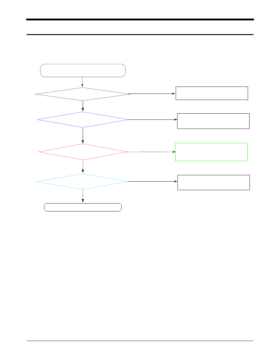
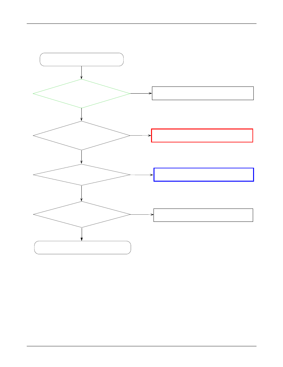
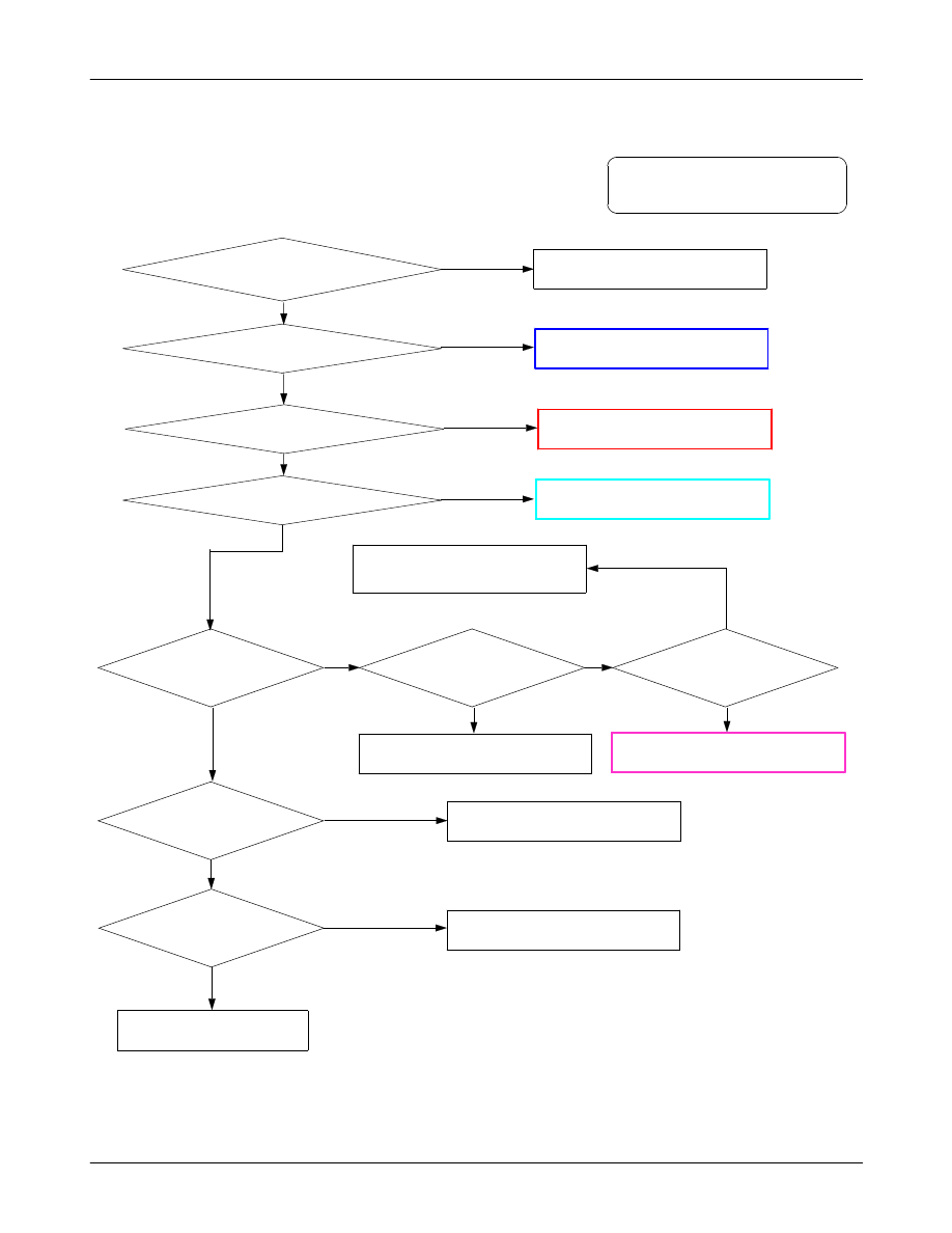
9-1-1. Power ON
Charge the battery
'Power ON' Does not work
Pin 3 of U301 is high?
If not, solder U301 again
or replace.
NO
NO
NO
YES
YES
YES
battery voltage > 3.6V
Voltage of Pin 5 of U301
> 3.3V
Voltage of TA314
>1.35V
Pin 1 of U307 is high?
If not, solder U307 again
or replace.
Check the initial operation
NO
Pin 3 of U302 is high?
If not, solder U302 again
or replace.
YES
Voltage of Pin 5 of U302
> 3V
SAMSUNG Proprietary-Contents may change without notice
Flow Chart of Troubleshooting and Circuit Diagrams
9-2
This Document can not be used without Samsung's authorization
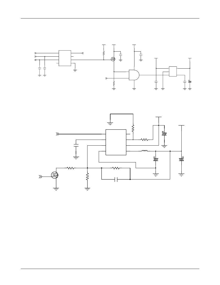
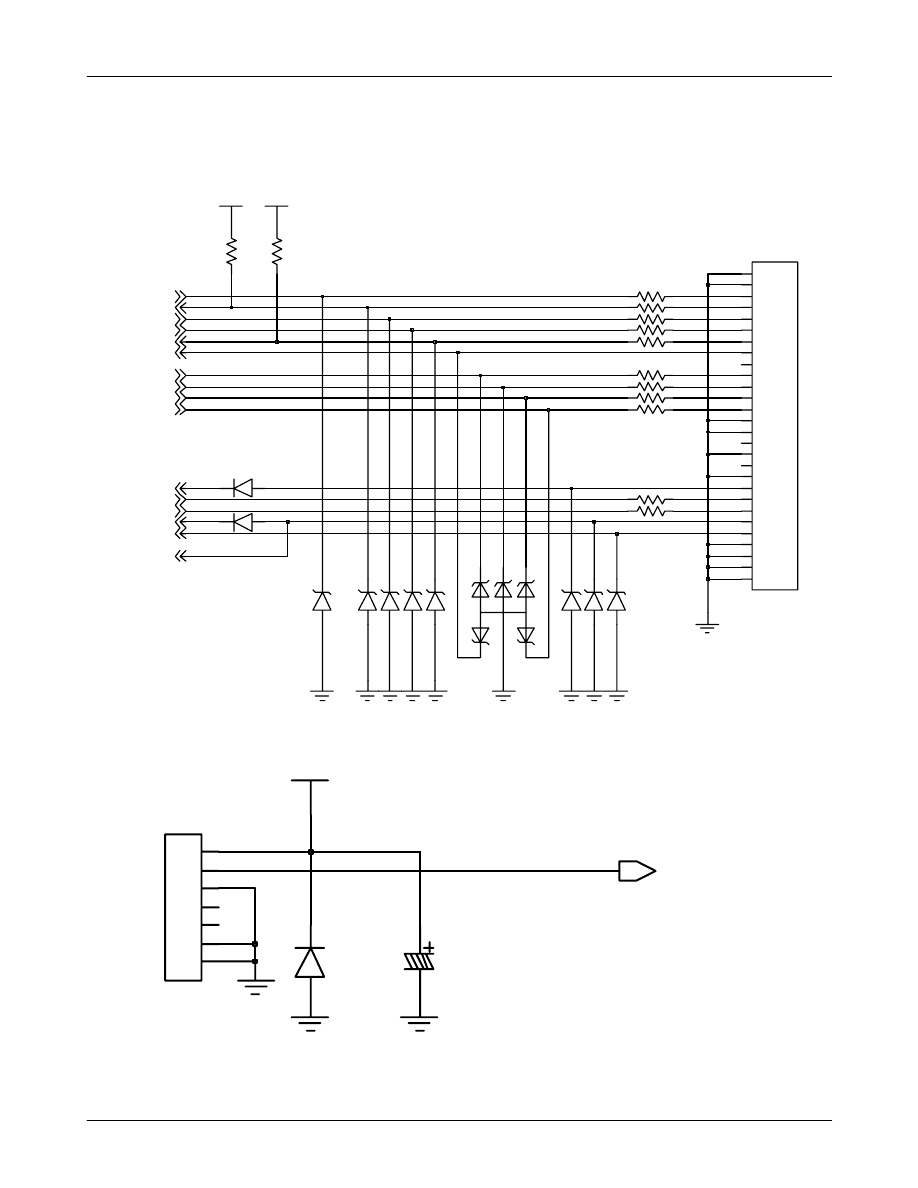
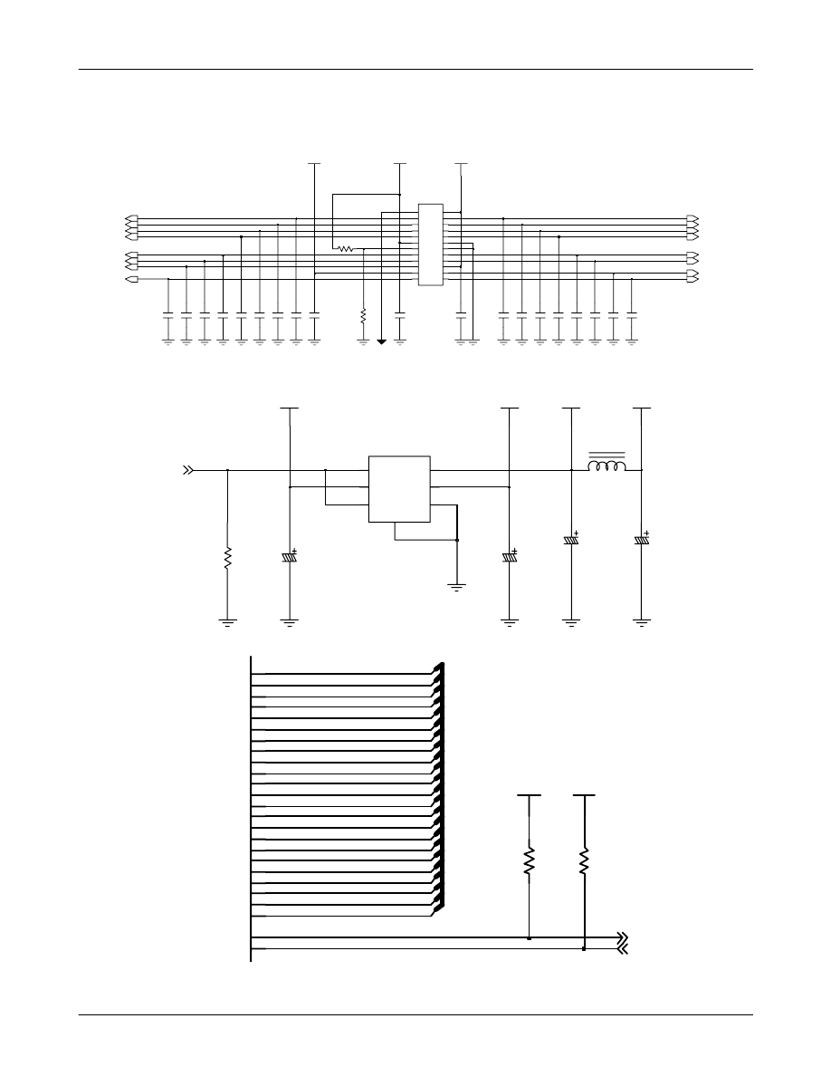
- Schematic for Power on
1.35V
TA314
R304
D
G
S
TR302
6
GND
4
ITH
2
PLLLPF
8
1
RUN
5
SW
7
S/MODE
3
VFB
VIN
U307
R307
L303
TA312
R315
R306
TA313
C308
VBAT
R305
CORE12
C309
VCORE_EN
PWR_EN
0505-001464 check
3.0V
VBAT
C305
BAT33
C306
D
3
G
1
S
2
R302
FDN338P
TR301
VBAT
C307
8 HOLE
PWR 1
6 SENSE
SW
7
C303
U306
2
DC
5 DEN
FET 3
GND 4
3
1
2
5
4
U304
1
OUT
5
REF_BYP
4
U301
3 EN
GND
2
IN
TA311
VBAT
C312
VBAT
C304
R303
POWER_DET
PDA_PWR_KEEP
AUTO_PWR
END_PWR
nPWR_SNS
SAMSUNG Proprietary-Contents may change without notice
Flow Chart of Troubleshooting and Circuit Diagrams
9-3
This Document can not be used without Samsung's authorization
-
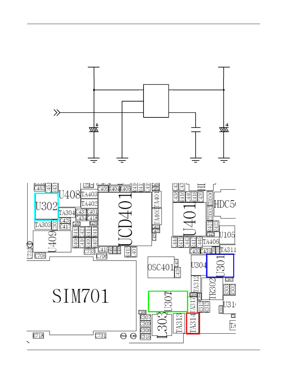
Layout for Power on
3.0V
TA303
VCC_CPU
C302
VBAT
TA304
5
REF_BYP
4
U302
3
EN
GND
2
IN
1
OUT
SYS_EN
SAMSUNG Proprietary-Contents may change without notice
Flow Chart of Troubleshooting and Circuit Diagrams
9-4
This Document can not be used without Samsung's authorization
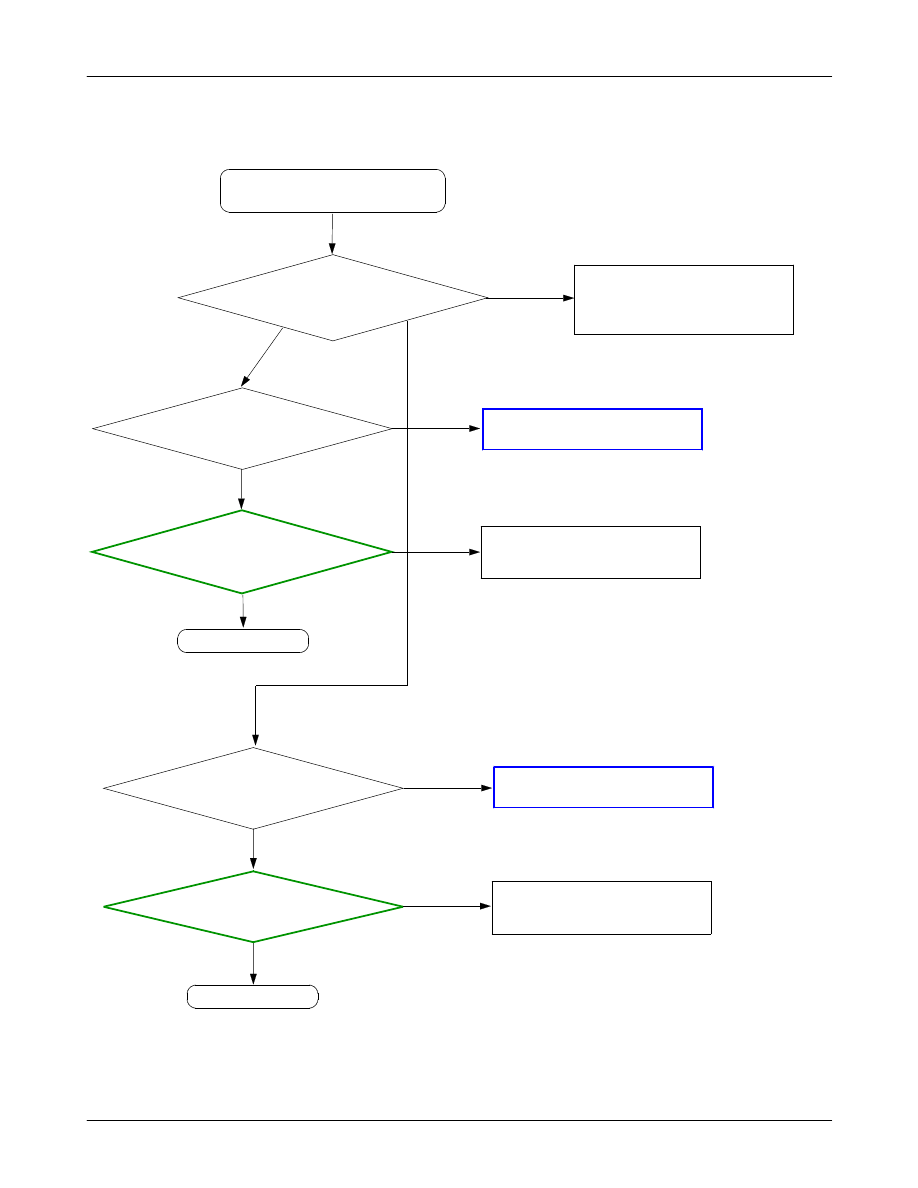
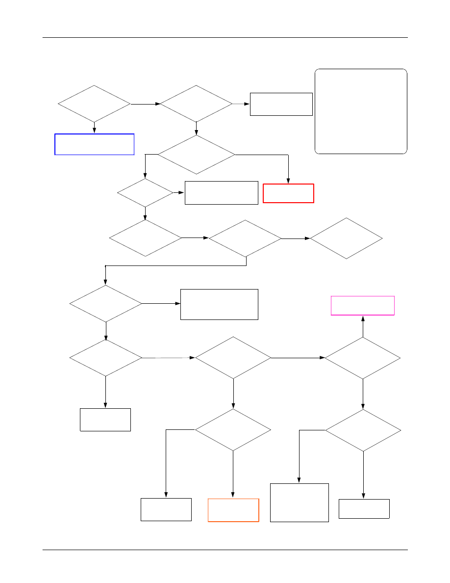
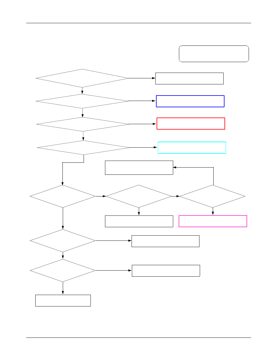
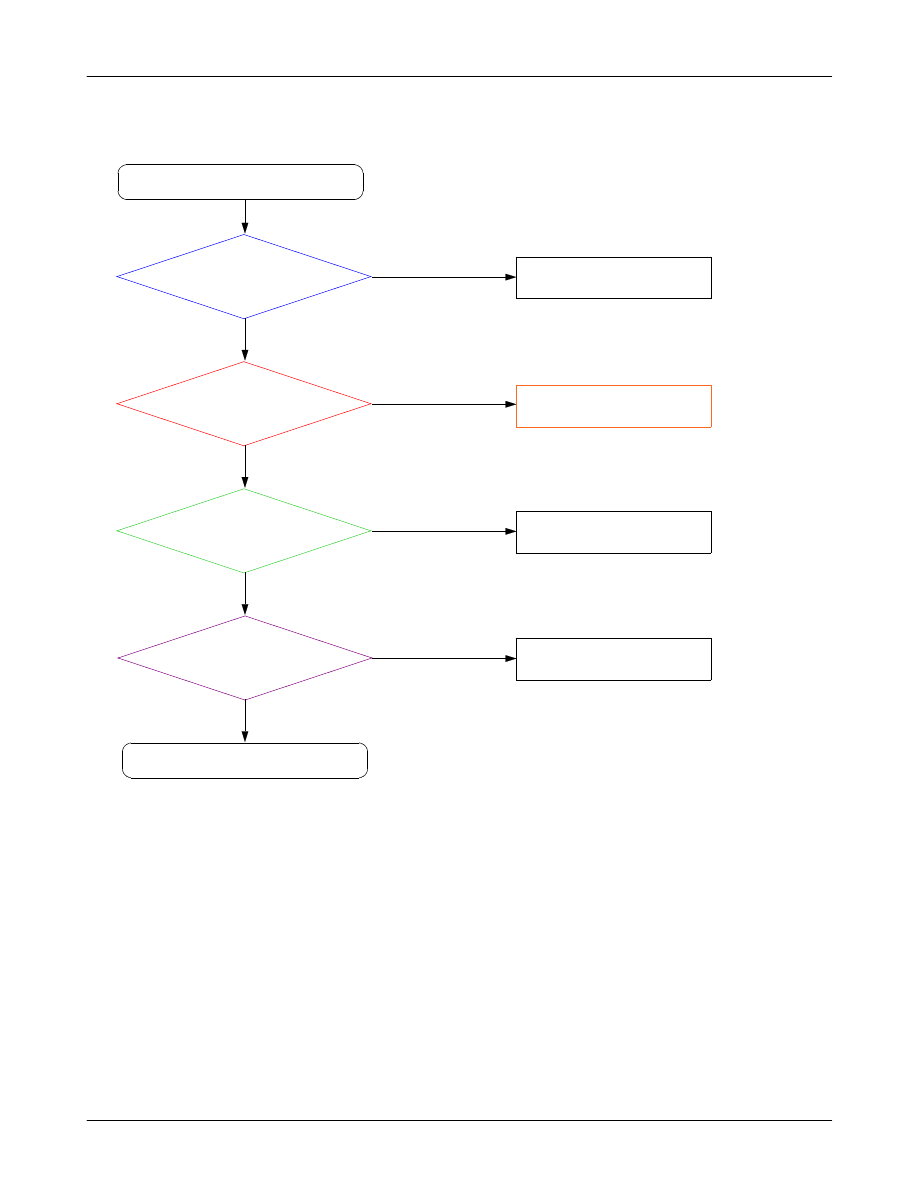
9-1-2. System Initial
YES
NO
NO
YES
YES
Check the Audio part
Check the LCD part
END
Sound operation OK ?
LCD Display OK ?
Initial Failure
Voltage of Pin 5 of U301
> 3.3V
NO
Pin 3 of U301 is high?
If not, solder U301 again
or replace.
YES
Voltage of TA314
>1.35V
NO
Pin 1 of U307 is high?
If not, solder U307 again
or replace.
YES
Voltage of Pin 5 of U302
> 3V
NO
Pin 3 of U302 is high?
If not, solder U302 again
or replace.
YES
Voltage of Pin 5 of L302
=1.8V
NO
Pin 3 of U305 is high?
If not, solder U305 again
or replace.
SAMSUNG Proprietary-Contents may change without notice
Flow Chart of Troubleshooting and Circuit Diagrams
9-5
This Document can not be used without Samsung's authorization
SAMSUNG Proprietary-Contents may change without notice
Flow Chart of Troubleshooting and Circuit Diagrams
9-6
This Document can not be used without Samsung's authorization
9-1-3. SIM Part
Check the voltage
at SIM701 pin #1 ≒ 2.8
"Please insert SIM card "
Check the SIM701's
Connection to SIM card
END
NO
Check the SIM Card
Solder SIM701 again or change
SIM701
YES
Check the UCD701
NO
YES
** Check SIM's signal
when you see SIM checking display
SAMSUNG Proprietary-Contents may change without notice
Flow Chart of Troubleshooting and Circuit Diagrams
9-7
This Document can not be used without Samsung's authorization
- Schematic for SIM connection
- Layout for SIM connection
VBAT
H11
VRTC
K12
VSIM
UP_IO
R10
UP_RST
J13
VDD12
C11
VDD34
01
C
5
D
D
V
31
B
76
D
D
V
K14
SIM_CLK
J11
SIM_IO
K11
SIM_RST
N9
UP_CLK
P10
8
E
Q
D
N
G
C732
C709
C731
R718
7
G
G
8
9
G
G
10
SIM701
1
1
2
2
3
3
4
4
5 5
6
6
C705
C733
C706
SIM_DET
SIMCLK
SIMRST
SIMDATA
SAMSUNG Proprietary-Contents may change without notice
Flow Chart of Troubleshooting and Circuit Diagrams
9-8
This Document can not be used without Samsung's authorization
9-1-4. Charging Part
Check the voltage of pin 23,24
of IFC601 = 4.2V
Replace TC
Abnormal charging operation
END
YES
NO
Check the voltage of BTC301
= 4.2V
NO
YES
Check the path from
BTC301
Charging
YES
SAMSUNG Proprietary-Contents may change without notice
Flow Chart of Troubleshooting and Circuit Diagrams
9-9
This Document can not be used without Samsung's authorization
- Schematic for Charging
NC
6
7
NC
BTC301
1
1
2
2
3
3
NC
4
5
NC
TA309
VBAT
ZD301
PWR_GND
R616
R612
NC
27
28
NC
4
4
5
5
6
6
7
7
8
8
9
9
NC
25
26
NC
19
19
2 2
20
20
21
21
22
22
23
23
24
24
3
3
11
11
12
12
13
13
14
14
15
15
16
16
17
17
18
18
IFC601
1
1
10
10
R619
R622
R609
VCC_CPU VCC_1.8V
D603
R623
R613
R610
31
6
D
Z
61
6
D
Z
51
6
D
Z
41
6
D
Z
11
6
D
Z
R621
R620
R629
R614
R624
01
6
D
Z
3
4
5
6
D602
ZD608
1
2
21
6
D
Z
PWR_GND
PDA_TMS
PDA_TDO
PDA_TCK
PDA_TDI
CHARGE_DET
VBAT
FFTXD
FFRXD
SDS_RXD
90
6
D
Z
VBAT
SDS_TXD
AUTO_PWR
USB_D+
USB_D-
VBUS

SAMSUNG Proprietary-Contents may change without notice
Flow Chart of Troubleshooting and Circuit Diagrams
9-10
This Document can not be used without Samsung's authorization
- Layout for charging
SAMSUNG Proprietary-Contents may change without notice
Flow Chart of Troubleshooting and Circuit Diagrams
9-11
This Document can not be used without Samsung's authorization
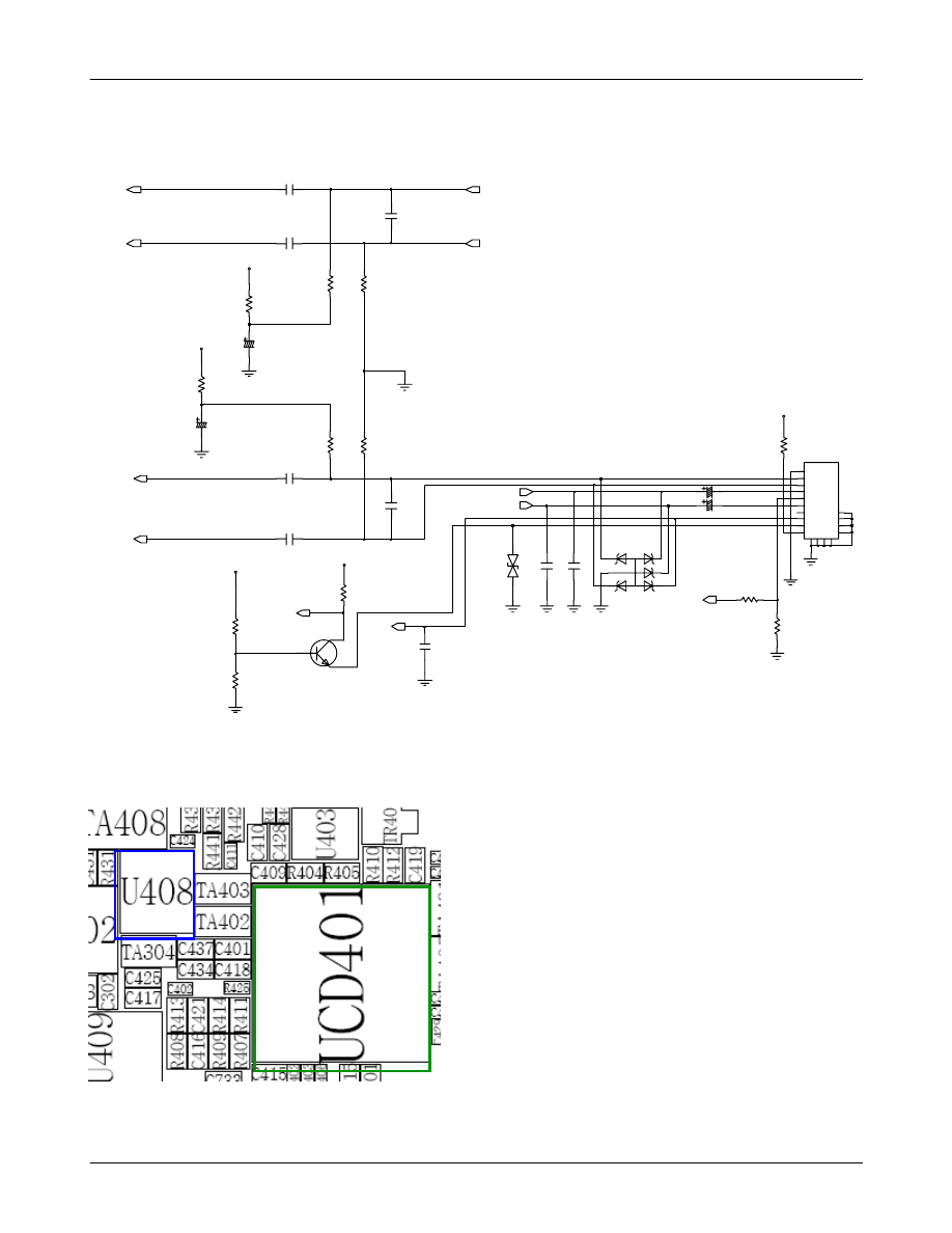
9-1-5. Microphone Part
Microphone does not work
Yes
No
Change Microphone or
Check Mic path soldering or
Download Image
Is there signal on the
C434,C437 during input signal
playing
If E/P = ON
END
Check the
Pin 1 of U408 is Low
Check the
Pin 29,23 of UCD401=
some signal on
Yes
Check UCD401 or Resolder
No
No
Check U408 or Resolder
Yes
If E/P = OFF
END
Check the
Pin 1 of U408 is High
Check the
Pin 23,30 of UCD401=
some signal on
Yes
Chech UCD401 or Resolder
No
No
Check U408 or Resolder
Yes
SAMSUNG Proprietary-Contents may change without notice
Flow Chart of Troubleshooting and Circuit Diagrams
9-12
This Document can not be used without Samsung's authorization
- Schematic for Microphone
- Layout for Speaker Part
MIC_N
SPK_P
P_BAT
SPK_COM
N.C
INT
ADC
SPK_N
P_GND
MIC_P
R440
C452
R437
R432
TA408
G 18
9
G
11 12
G
G
13 14
G
G
15
16
G
17
G
10
2
3
4
5
6
7
8
EAR401
1
R431
R430
BAT33
R426
C456
C434
R427
ZD402
1
2
3
4
5
6
TA410
BAT33
C453
R435
BAT33
R433
C436
C454
C448
R429
AUDIO30
TA407
R436
AUDIO30
1
TR402
2
3
TA409
C437
30
4
D
Z
C451
R439
SEND_END
EAR_SPKL
JACK_S
NC_GND
MIC-
MICINN
AUXINP
AUXINN
MICINP
MIC+
EAR_SPKR
SAMSUNG Proprietary-Contents may change without notice
Flow Chart of Troubleshooting and Circuit Diagrams
9-13
This Document can not be used without Samsung's authorization
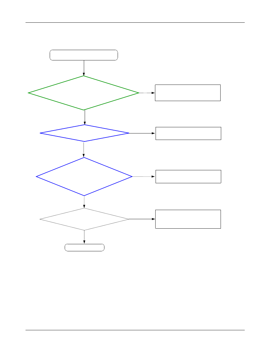
9-1-6. Speaker Part
Speaker does not work
Yes
Is there sinewave
signal on the UCD401 pin 39,
41
during window
media playing?
No
Check UCD401 or Resolder
Yes
No
Check the
Pin 1,13 of U401 is High
Check U401 or Resolder
Yes
No
Check U401 or Resolder
Is there signal
on the U401 Pin 4,6,16,18
during window media playing
Yes
No
Replace the speaker
Check the speaker
= out of order or not
Yes
END

SAMSUNG Proprietary-Contents may change without notice
Flow Chart of Troubleshooting and Circuit Diagrams
9-14
This Document can not be used without Samsung's authorization
- Schematic for Speak part
60
5
D
Z
50
5
D
Z
7
8
8
9
9
15
15
16 16
2
2
3
3
4
4
5
5
6
6
7
HDC502
1
1
10
10
11
11
12
12
13 13
14
14
20
5
D
Z
C511
C510
30
5
D
Z
MSPKRN
MSPKRP
FLASH_LED-
MSPKLP
MSPKLN
FLASH_LED+
TA406
C445
C439
C443
C440
VDD
9
C442
25
GND
NC
26
27
NC
VDD
3
VOMR
4
VSS
5
VOPR
6
VDD
7
VSS
8
VDD
19
VSS
2
VSS
20
VDD
21
VIML
22
VREFL
23
VIPL
24
VREFR
11
VIPR
12
EN_R
13
VSS
14
VDD
15
VOML
16
VSS
17
VOPL
18
U401
EN_L
1
VIMR
10
C444
C430
C433
C432
C431
R417
VBAT
R416
R420
C438
R422
R419
R418
R421
R423
SAPA_EN
SAPA_EN
MSPKRN
MSPKRP
LOUD_GNDL
LOUD_GNDR
MSPKLN
MSPKLP
LOUD_SPKL
LOUD_SPKR
SAMSUNG Proprietary-Contents may change without notice
Flow Chart of Troubleshooting and Circuit Diagrams
9-15
This Document can not be used without Samsung's authorization
- Layout for Speaker Part
SAMSUNG Proprietary-Contents may change without notice
Flow Chart of Troubleshooting and Circuit Diagrams
9-16
This Document can not be used without Samsung's authorization
9-1-7. Receiver Part
Receiver does not work
No
Check UCD401 or Resolder
Check the
Pin 23,24 of UCD401 = some
signal on
Yes
Check the
Pin 35,36 of UCD401=
some signal on
Check UCD401 or Resolder
No
Yes
Check U409 or Resolder
No
Check the
Pin 2,10 of U409=
some signal on
Yes
Resoldering R434,R438
Check the
R434,R438 =
some signal on
No
Yes
Replace the Receiver
No
Check the
Receiver = Out of order or
not
Yes
END
SAMSUNG Proprietary-Contents may change without notice
Flow Chart of Troubleshooting and Circuit Diagrams
9-17
This Document can not be used without Samsung's authorization
- Schematic for Receiver part
C402
AUDIO30
IN2
8
5
NC1
7
NC2
NO1
2
NO2
10
1
V+
U409
3
COM1
9
COM2
6
GND
IN1
4
EAR_SPKL
EAR_RCVN
EAR_RCVP
JACK_S
JACK_S
EAR_SPKR
RCVN
RCVP
MAIN MP3
MAIN RCV
EAR MP3
EAR RCV
53
R
K
P
S
63
SPKVDD
83
OUT3
73
33
4
T
U
O
D
N
G
K
P
S
43
L
K
P
S
03
O
N
O
M
13
HPL
93
2
P
A
C
23
MIC_WM_OUTP
LOUD_SPKL
MIC_WM_OUTN
P
O
P_
R
A
E
EAR_RCVN
EAR_RCVP

SAMSUNG Proprietary-Contents may change without notice
Flow Chart of Troubleshooting and Circuit Diagrams
9-18
This Document can not be used without Samsung's authorization
- Layout for Receiver Part
C455
ZD401
TP402
R434
R438
C457
ZD404
TP401
RCVP
RCVN
SAMSUNG Proprietary-Contents may change without notice
Flow Chart of Troubleshooting and Circuit Diagrams
9-19
This Document can not be used without Samsung's authorization
9-1-8. Headset Part
Headset Function does not work
Check the
Pin 20,21 of UCD401 = some
signal on
No
Check UCD401 or Resolder
Yes
Check the
Pin 35,36 of UCD401=
some signal on
Check UCD401 or Resolder
No
Yes
Check the
Pin 5,7 of U409 = some
signal on
Check U409 or Resolder
No
Yes
Resoldering TA409,TA410
No
Check the
TA409,TA410 =
some signal on
Yes
Resoldering Ear401
No
Check the
Ear401 connection = Out of
order or not
Yes
Check the Ear mic
= Out of order or not
Use other Ear mic
No
Yes
END
SAMSUNG Proprietary-Contents may change without notice
Flow Chart of Troubleshooting and Circuit Diagrams
9-20
This Document can not be used without Samsung's authorization
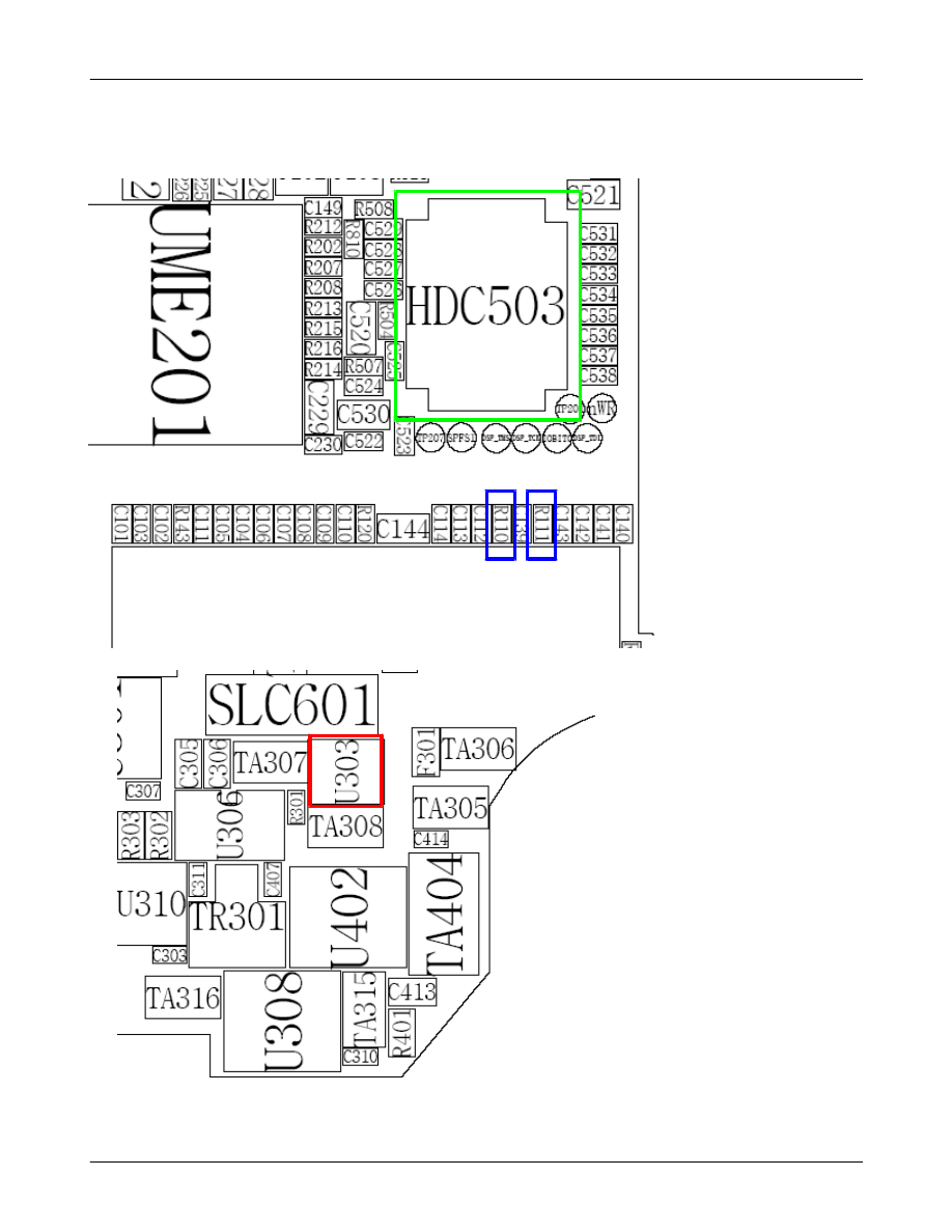
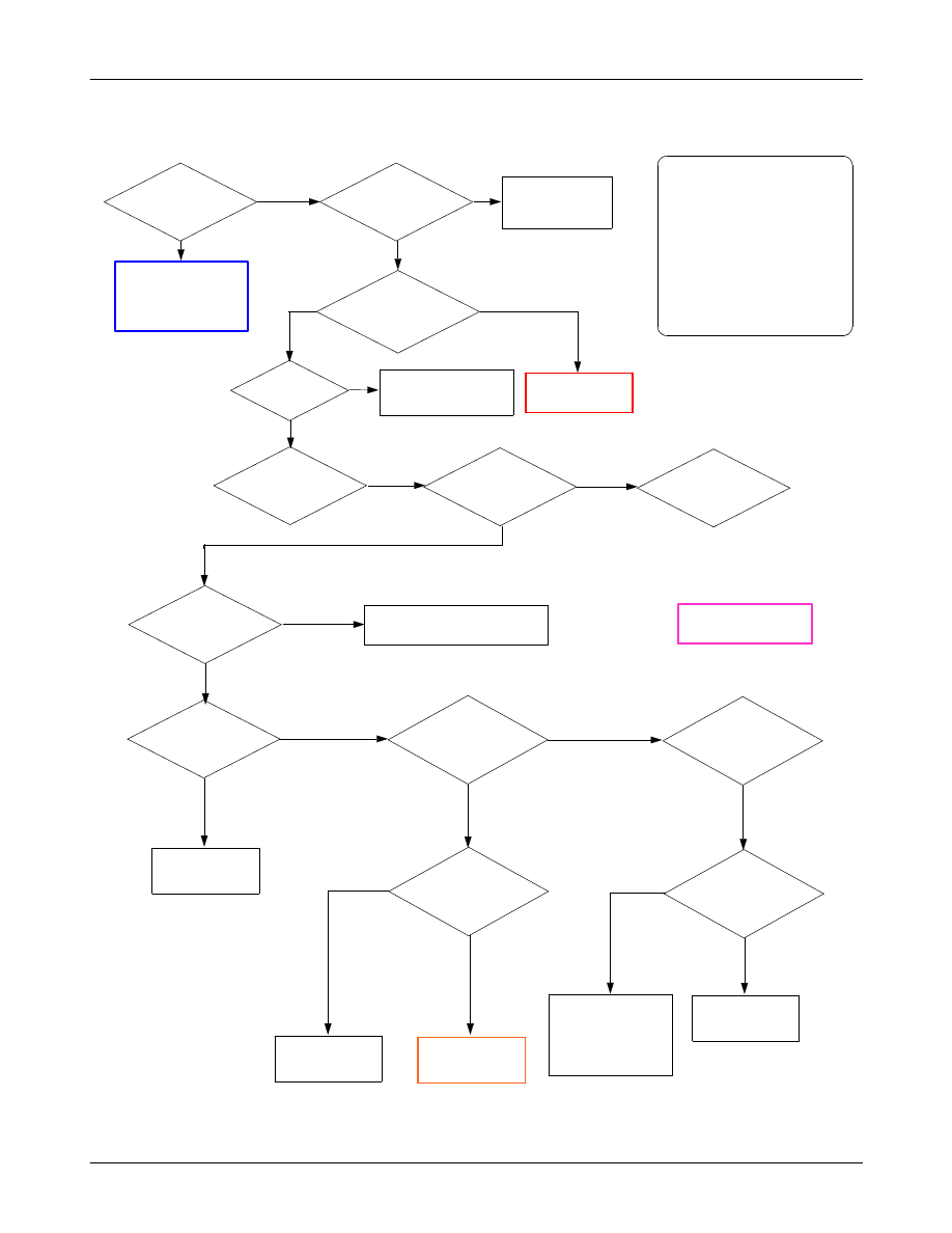
9-1-9. Camera Part (Mega and VGA)
Camera function does not work
Check the
connection between
a camera module
and HDC503
NO
Re-connect the camera module
NO
NO
NO
YES
YES
Check the R110, R111
Check the UCP100
Check U303
YES
YES
Replace a Camera module & END
Check voltages of HDC503
pin 11 : 2.8V
pin 2 : 1.8V
Check voltages of HDC503
pin 23,24 : 3V
Examine the HDC 503
to find any soldering defect.
SAMSUNG Proprietary-Contents may change without notice
Flow Chart of Troubleshooting and Circuit Diagrams
9-21
This Document can not be used without Samsung's authorization
- Schematic for CAMERA
2.8V
1.8V
2.8V
CAM_DVDD_H18
VBAT
R301
F301
TA307
CAM_DVDD_H28
TA308
CAM_AVDD_H28
TA305
VOUT2 6
VSS 4
U303
3
EN1
EN2
1
7
D
N
G
VIN
2
VOUT1 5
TA306
CAM_EN
C534
24
3 3
4 4
5
5
6
6
7 7
8 8
9
9
17
18
18
19 19
2
2
20 20
21
21
22
22
23 23
24
1
10
10
11 11
12 12
13
13
14
14
15 15
16 16
17
HDC503
1
C526
C523
C521
CAM_AVDD_H28
R504
CAM_DVDD_H28
C535
C529
C528
C533
C525
C524
C520
CAMAGND
C536
C538
CAM_DVDD_H18
C532
R507
C522
C531
C530
C527
C537
CAM_PCLK
CAM_MCLK
CAM_ENB
CAM_RESETB
CAM_SCLK
CAM_SDA
Y(5)
Y(7)
Y(6)
Y(4)
Y(2)
Y(0)
Y(3)
Y(1)
CAM_VSYNC
CAM_HSYNC
PU
PU
SCL_GPIO117
E2
B1
SDA_GPIO118
MA5
MA6
N5
R6
MA7
MA8
T7
P5
MA9
R4
MA19
MA2
MA20
T4
W5
MA21
MA22
Y4
W4
MA23
MA24
W2
V2
MA25
P6
MA3
MA4
R7
W8
P4
MA10
W7
MA11
MA12
T6
U6
MA13
MA14
V6
R5
MA15
MA16
T5
W6
MA17
MA18
P2
VCC_CPU
VCC_CPU
R111
R110
MA(9)
MA(8)
MA(7)
MA(6)
MA(5)
MA(4)
MA(3)
MA(25)
MA(24)
MA(23)
MA(22)
MA(21)
MA(20)
MA(19)
MA(18)
MA(17)
MA(16)
MA(15)
MA(14)
MA(13)
MA(12)
MA(11)
MA(10)
CAM_SDA
CAM_SCLK
SAMSUNG Proprietary-Contents may change without notice
Flow Chart of Troubleshooting and Circuit Diagrams
9-22
This Document can not be used without Samsung's authorization
- Layout for CAMERA

SAMSUNG Proprietary-Contents may change without notice
Flow Chart of Troubleshooting and Circuit Diagrams
9-23
This Document can not be used without Samsung's authorization
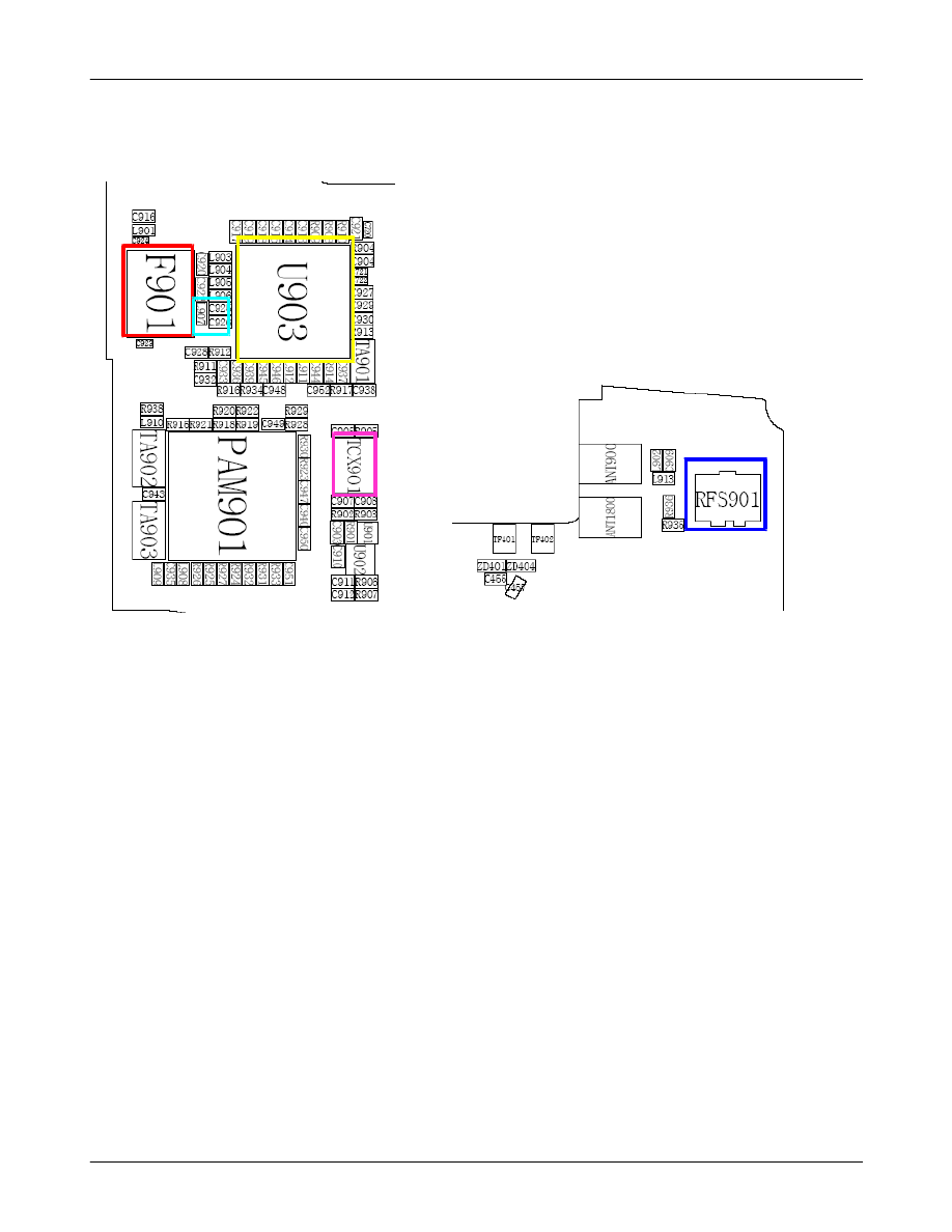
9-2.RF
9-2-1. EGSM Receiver
Continuous RX on
RFinput : 62CH AMP :
-50dBm
Yes
Yes
No
Yes
Yes
Yes
Check UCD701
U903 check or resolder
UCD701 pin B10, C736
Check or resolder
TCX901
change or resolder
C907, R902
check or resolder
No
No
U903 check
pin 25,26,27,28
Vp-p:100mV
U903 check
pin 1,8,31,36,41
clean 2.8V
No
No
UCD701 pin A13, C735
check or resolder
TCX901 check
pin 4 = clean 3V?
TCX701 check
pin3 = 26M ?
Vp-p : 1V
U903 check
pin 35 = 26M ?
Vp-p : 860mV
C925, C926, L907
resolder or change
No
U903 check
pin 6,7 = -65dBm
Yes
F901 resolder or
change
No
F901 check
pin 1,2 = -65dBm
Yes
RFS901 resolder or
change
No
F901 check
pin13 = -65dBm
Yes
Check soldered status
of C916,L901
No
Normal
Condition catch
the channel?
Yes
SAMSUNG Proprietary-Contents may change without notice
Flow Chart of Troubleshooting and Circuit Diagrams
9-24
This Document can not be used without Samsung's authorization
9-2-2. EGSM Transmitter
Continuous TX on
CONDITION TX POWER
DAC500 CODE APPLIED
CH62
RBW : 100KHz
VBW : 100KHz
SPAN : 10MHz REF
LEV : 10dBm ATT :
20dB
UCD701 check
or change
No
No
F901
pin11=2.8V?
F901 pin10
about 2-3dBm?
RFS901,C933,L901
check or change
No
No
No
No
No
Yes
Yes
No
Yes
No
No
Yes
No
Yes
No
Yes
Yes
TCX901 check
or resolder
UCD701 pin
A13,C735
change or
resolder
U903 change
or resolder
U903 change
or resolder
UCD701
change
or resolder
PAM901
change
or resolder
TCX901
Pin4:3V?
U903 pin
32,33
=3V?
UCD701
pinA13,C735
cgange or resolder
TCX901
pin3 : 26MHz?
Vp-p:1V
F901 check
or change
Between
F901,PAM901
1.2V?
Between
F901,C923
≒
4~5dBm?
Yes
Yes
Yes
Yes
U903 pin
35:26MHz?
Vp-p:860mV
U903
pin25,26,27,28=
1.7V?
U903
pin1,8,31,36,41=
2.8V?
UCD701
check or
change
Battery,UCD701
check or change
F901 check
or change
TA902:3.7V
SAMSUNG Proprietary-Contents may change without notice
Flow Chart of Troubleshooting and Circuit Diagrams
9-25
This Document can not be used without Samsung's authorization
9-2-3. DCS Receiver
Continuous RX on
RFinput : 698CH AMP :
-50dBm
No
Yes
Yes
No
Yes
Yes
Yes
Check UCD701
U903 check or resolder
UCD701 pin B10, C736
Check or resolder
TCX901 change or resolder
C907, R902
check or resolder
No
No
U903 check
pin 25,26,27,28
Vp-p : 100mV
U903 check
pin 1,8,31,36,41
clean 2.8V
No
No
UCD701 pin A13,C735
check or resolder
TCX901 check
pin 4 = clean 3V?
TCX901 check
pin3 = 26M ?
Vp-p : 1V
U903 check
pin 35 = 26M ?
Vp-p : 860mV
C922, L905, L906
resolder or change
No
U903 check
pin 4,5 = -65dBm
Yes
F901 resolder or
change
No
F901 check
pin 3,4 = -65dBm
Yes
RFS901 resolder or
change
No
F901 check
pin13 = -65dBm
Yes
Check soldered status
of C916,L901
Normal
Condition catch
the channel?
Yes
SAMSUNG Proprietary-Contents may change without notice
Flow Chart of Troubleshooting and Circuit Diagrams
9-26
This Document can not be used without Samsung's authorization
9-2-4. PCS Receiver
Continuous RX on
RFinput : 660CH AMP :
-50dBm
No
Yes
Yes
No
Yes
Yes
Yes
Check UCD701
U903 check or resolder
UCD701 pin B10, C736
Check or resolder
TCX901 change or resolder
C907, R902
check or resolder
No
No
U903 check
pin 25,26,27,28
Vp-p : 100mV
U903 check
pin 1,8,31,36,41
clean 2.8V
No
No
UCD701 pin A13, C735,
C710
check or resolder
TCX901 check
pin 4 = clean 3V?
TCX901 check
pin3 = 26M ?
Vp-p : 1V
U903 check
pin 35 = 26M ?
Vp-p : 860mV
C920, L903, L904
resolder or change
No
U903 check
pin 2,3 = -65dBm
Yes
F901 resolder or
change
No
F901 check
pin 5,6 = -65dBm
Yes
RFS901 resolder or
change
No
F901 check
pin13 = -65dBm
Yes
Check soldered status
of C916,L901
Normal
Condition catch
the channel?
Yes
SAMSUNG Proprietary-Contents may change without notice
Flow Chart of Troubleshooting and Circuit Diagrams
9-27
This Document can not be used without Samsung's authorization
9-2-5. DCS, PCS Transmitter
Continuous TX on
CONDITION
CH:698CH(DCS)
CH:660CH(PCS)
TX POWER CODE :
350CODE APPLIED
RBW : 100KHz
VBW : 100KHz
SPAN : 10MHz REF
LEV : 10dBm ATT :
20dB
U903 pin
35:26MHz?
Vp-p:860mV
UCD701 pinA13,C735
change or resolder
TA902:3.7V
UCD701
check
or change
No
No
No
No
Yes
Yes
No
Yes
No
No
Yes
No
Yes
No
Yes
No
No
Yes
F901
pin2=2.8V?
TCX901 check
or resolder
UCD701 pin
A13,C735
change or
resolder
U903 change
or resolder
U903 change
or resolder
UCD701
change
or resolder
PAM901
change
or resolder
TCX901
Pin4:3V?
U903
pin 32,33
=3V?
TCX901
pin3 : 26MHz?
Vp-p:1V
U903
pin25,26,27,28
=1.7V?
U903
pin1,8,31,36,41
32=2.8V?
F901 check
or change
Between
F901,PAM901
1.2V?
F901 check
or change
Battery,UCD701
check or change
Between
F901,C924
≒
4~5dBm?
RFS901,C933,
L901
check or change
UCD701 check
or change
F901 pin10
about 2-3dBm?
Yes
Yes
Yes
Yes
SAMSUNG Proprietary-Contents may change without notice
Flow Chart of Troubleshooting and Circuit Diagrams
9-28
This Document can not be used without Samsung's authorization
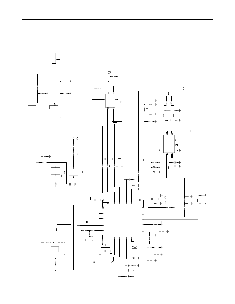
**If you check the tx chain,
Check the not only RF Device but also resistor, inductor and capacitor.
-schematic for RF part
C
92
8
C
90
3
C
92
0
C
93
7
5
6
V
C
C
4
Y
U
90
1
A
2
3
G
N
D
1
N
C
N
C
R
92
7
R
93
8
V
B
A
T
C
91
6
V
P
A
C
_
2.
8V
C
93
9
V
R
F
_2
.8
V
R
91
6
V
R
F
_2
.8
V
V
S
Y
N
_2
.8
V
R
9
03
R
92
9
R
92
8
C
9
51
C
90
9
L9
13
L
90
6
V
R
F
_
2.
8V
C
93
5
L
90
4
C
94
0
10
N
F
R
91
5
5
_Q
V
P
A
C
_2
.8
V
L
90
8
C
K
7
D
6
G
N
D
4
Q
3
8
V
C
C
_C
L
R
2
1
_P
R
C
94
7
V
R
F
_2
.8
V
U
9
02
V
C
C
V
C
X
O
36
V
C
X
O
B
35
V
C
X
O
O
U
T
1
34
2
T
U
O
O
X
C
V
3
7
V
C
C
LN
A
1
48
X I M
C
C
V
O
L
F
R
C
C
V
43
N
Y
S
F
R
C
C
V
41
42
O
C
V
F
R
C
C
V
V
C
C
T
X
1
8
22
2
X
T
C
C
V
16
O
C
V
X
T
C
C
V
S
D
A
T
A
33
21
N
O
X
T
D
T
U
O
X
T
1
8
17
G
T
U
O
X
T
20
G
O
C
V
X
T
19
B
G
O
C
V
X
T
V
C
C
B
B
31
V
C
C
IF
S
Y
N
29
N
C
54
P
C
S
LN
A
I
2
P
C
S
LN
A
IB
3
23
W
B
M
P
24
O
T
E
D
M
P
Q
O
U
T
B
/Q
IN
B
25
Q
O
U
T
/Q
IN
26
15
C
A
D
P
M
A
R
G
52
G
S
M
LN
A
I
6
G
S
M
L
N
A
IB
7
IO
U
T
B
/II
N
B
27
IO
U
T
/II
N
28
LD
O
_C
O
N
T
12
38
E
L
53
N
C
D
C
S
LN
A
I
4
D
C
S
LN
A
IB
5
D
M
IX
IN
9
D
M
IX
IN
B
10
K
C
O
L
F
39
G
4
9
G
50
51
G
B
IA
S
D
A
C
11
I P
A
C
47
46
B I P
A
C
Q
P
A
C
45
44
B
Q
P
A
C
C
LK
32
C
P
IF
S
Y
N
30
40
N
Y
S
F
R
P
C
U
9
03
14
O
T
E
D
M
A
13
T
N
O
C
_
M
A
C
91
8
C
91
3
C
92
5
L9
0
7
V
B
A
T
16
V
D
D
_I
C
V
ID
O
15
V
R
A
M
P
5
V
R
E
G
3
V
T
X
O
N
6
5 2
1
D
N
G
4
9
1
C
N
1
P
IN
_D
C
S
|P
C
S
7
P
IN
_G
S
M
P
O
U
T
_D
C
S
|P
C
S
19
13
P
O
U
T
_G
S
M
2
V
B
A
N
D
17
0 1
G
1 1
G
4 1
G
0 1
1 1
G
G
1 2
2 2
G
G
3 2
4 2
G
G
P
A
M
9
01
C
O
U
P
L
E
R
O
U
T
_D
C
S
|P
C
S
20
C
O
U
P
LE
R
O
U
T
_G
S
M
12
G
8
8 1
R
92
0
4
4
5
5
6
6
R
93
4
9
A
N
T
90
0
1
1
2
2
3
3
4
G
S
M
18
00
/1
9
00
_T
X
8
5
G
S
M
19
0
0_
R
X
1
G
S
M
19
0
0_
R
X
2
6
1
G
S
M
90
0
_R
X
1
G
S
M
90
0
_R
X
2
2
10
G
S
M
90
0_
T
X
V
C
1
11
V
C
2
F
90
1
13
A
N
T
G
7
G
14
12
G
G
15
16
G
3
G
S
M
18
0
0_
R
X
1
G
S
M
18
0
0_
R
X
2
R
92
3
T
C
X
90
1
2
D
N
G
T
U
O
4
3
C
C
V
N
O
C
V
1
R
90
7
C
90
4
C
9
32
3 3 9
C
C
94
6
C
93
6
C
94
9
R
93
3
R
93
0
1 1 9 L
R
92
6
C
92
9
C
93
0
T
A
90
1
C
92
7
C
92
1
R
90
1
C
92
4
T
A
90
3
R
92
5
R
92
1
R
93
1
R
90
9
R
91
8
R
91
3
R
91
0
R
91
4
C
9
23
L9
10
R
93
2
R
91
7
0 5 9
C
R
90
5
R
92
4
C
91
0
R
93
5
2 1 9 L
4
4
5
5
6
6
C
94
4
4
A
N
T
18
00
1
1
2
2
3
3
R
F
S
90
1
2
A
C
3
G
1
G
C
91
2
R
90
2
R
90
4
V
S
Y
N
_2
.8
V
R
90
6
V
R
F
_2
.8
V
C
90
7
V
R
F
_2
.8
V
C
90
5
T
A
90
2
C
94
5
C
92
2
C
92
6
C
90
8
C
93
8
R
93
6
L9
01
L9
03
R
91
2
C
95
2
L9
02
C
91
1
R
91
1
C
91
7
L9
09
C
91
9
C
9
15
R
91
9
R
92
2
C
94
3
C
91
4
C
94
8
B
A
N
D
S
E
L
T
X
_D
P
C
S
_E
N
A
N
T
R
90
8
T
X
_G
S
M
_E
N
S
E
R
LE
R
X
T
X
IN
_G
R
X
T
X
IP
_G
R
X
T
X
Q
N
_G
R
X
T
X
Q
P
_G
T
X
P
S
E
R
D
A
T
A
F
C
C
LK
13
M
_C
S
P
C
LK
13
M
_T
R
S
E
R
C
LK
SAMSUNG Proprietary-Contents may change without notice
Flow Chart of Troubleshooting and Circuit Diagrams
9-29
This Document can not be used without Samsung's authorization
-Layout for RF part
SAMSUNG Proprietary-Contents may change without notice
Flow Chart of Troubleshooting and Circuit Diagrams
9-30
This Document can not be used without Samsung's authorization
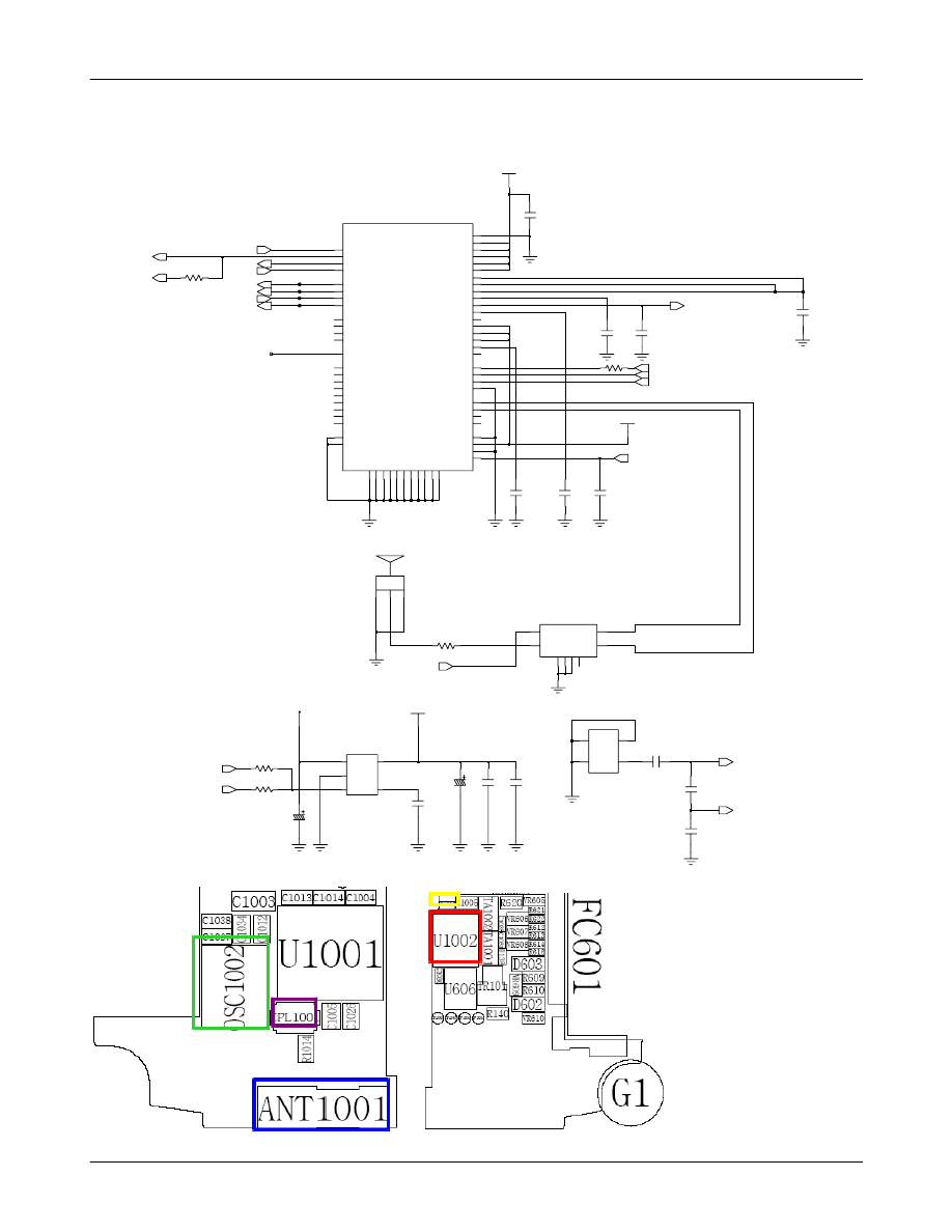
9-2-6. BLUETOOTH
Bluetooth Activation
Has the BT Ant
no crack?
BT Ant
Resolder or Change
YES
NO
Check U1002
Pin #5 = 3V?
YES
NO
Check the R1006
Check OSC1002
Pin #3 has 13MHz
signal?
YES
NO
Resolder OSC1002
Check CPL1001's
Pin #3 output > -6dBm
YES
NO
Change CPL1001
The End
SAMSUNG Proprietary-Contents may change without notice
Flow Chart of Troubleshooting and Circuit Diagrams
9-31
This Document can not be used without Samsung's authorization
3.0V
C1004
C1005
2
G
5
A
S
S
V
6
A
S
S
V
3
F
XTALM E1
E2
XTALP|FAST_CLK_IN
VDD_IO_SF2
B3
G5
VLDO_OUT
1
S
S
V
8
B
8
G
2
S
S
V
7
H
3
S
S
V
4
S
S
V
5
A
5
S
S
V
2
A
4
F
1
A
S
S
V
4
H
2
A
S
S
V
1
D
3
A
S
S
V
4
A
S
S
V
1
G
G4
A8 TX_DBG
H6
VBAT
VDD_IN_ANA
C2
F5
VDD_IN_BB
H3
VDD_IN_OSC
VDD_IN_RFIO
F1
D8
VDD_IO1
G7
VDD_IO2_1
VDD_IO2_2
A3
VDD_IO_SF1
H8
B5 JTAG_TMS
G6
KA_OUT
NC1
1
2
NC2
NSHUT_DOWN E3
G3
OSC_LDO_OUT
RFIO_LDO_OUT
F2
H2
RFM
H1
RFP
F6
SLOW_CLK_IN
TL_LDO_OUT
B4 IO14
IO15
F7
C6 IO1|EXT_CLK_REQ_IN
IO2|SCL
B7
D5 IO3|SDA
IO4
A6
C4 IO5
IO7
C8
D4 JTAG_TCK
JTAG_TDI
C3
E6
JTAG_TDO
F8
H5
BB_LDO_OUT2
BB_LDO_OUT3
A4
BGAP_I
A1
B1
BGAP_V
D6
EMRST
E8 HCI_CTS
HCI_RTS
E7
HCI_RX
E4
E5 HCI_TX
IO0|EXT_CLK_REQ_OUT
D7
ANATEST1 B2
ANATEST2
C1
ANA_LDO_OUT
D2
B6
AUD_CLK
AUD_FSYNC
A7
AUD_IN
C5
C7 AUD_OUT
BB_LDO_OUT1
TA1001
U1001
TA1002
C1038
VBT
C1027
VBAT
C1036
OSC1002
2
1
D
N
G
2
D
N
G
4
T
O
H
1
3
T
O
H
TP1004
TP1005
C1013
4
TP1002
TP1003
U1002
3
EN
GND
2
IN
1
OUT
5
C1028
C1034
C1031
R1006
R1005
C1001
6
G
G
7
8
G
NC
1
UNBAL
3
CPL1001
4
BAL
BAL 5
2 DC
C1014
1
3
2
C1003
R1014
ANT1001
VBT
VBT
R1008
TP1001
R1009
CPU_WAKEUP
BT_PWREN
C1012
BTRXD
BTTXD
BTCTS
BTRTS
XTALINM
XTALINP
PCM_CLK
PCM_FSYNC
PCM_IN
PCM_OUT
BT_RESET
BT_CLK32
SYS_EN
XTALINP
XTALINM
RFIO_LDO_OUT
RFIO_LDO_OUT
Wyszukiwarka
Podobne podstrony:
20061127143400093 GH68 10798A Preca 2
20061127143400093 GH68 10798A Suppl 17
20061127143400093 GH68 10798A rinfo 3
20061127143400093 GH68 10798A COVER 1
200611290001 7 7
200611290001 7 14
C7 200611 CAT PL
200611290001 7 6
200611290001 7 18
200611290001 7 1
SGH X105NBATMB SM ST GH68 04199A TSHOO 9
GH68 10734A TSHOO 9
200611290001 7 2
więcej podobnych podstron