Document Number: 83673
For technical questions, contact: optocoupler.answers@vishay.com
www.vishay.com
Rev. 1.9, 10-Dec-08
651
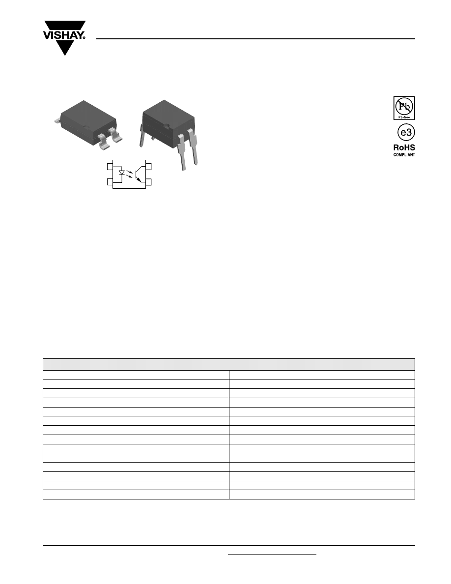
Optocoupler, Phototransistor Output,
Low Input Current
SFH618A, SFH6186
Vishay Semiconductors
DESCRIPTION
The SFH618A (DIP) and SFH6186 (SMD) feature a high
current transfer ratio, low coupling capacitance and high
isolation voltage. These couplers have a GaAs infrared diode
emitter, which is optically coupled to silicon planar
phototransistor detector, and is incorporated in a plastic
DIP-4 or SMD package.
The coupling devices are designed for signal transmission
between two electrically separated circuits.The couplers are
end-stackable with 2.54 mm lead spacing. Creepage and
clearance distances of > 8.0 mm achieved with option 6. This
version complies with IEC 60950 (DIN VDE 0805) for
reinforced insulation to an operation voltage of 400 V
RMS
or
DC.
FEATURES
• Good CTR linearity depending on forward
current
• Low CTR degradation
• High collector emitter voltage, V
CEO
= 55 V
• Isolation test voltage, 5300 V
RMS
• Low coupling capacitance
• End stackable, 0.100" (2.54 mm) spacing
• High common mode transient immunity
• Lead (Pb)-free component
• Component in accordance to RoHS 2002/95/EC and
WEEE 2002/96/EC
APPLICATIONS
• Telecom
• Industrial controls
• Battery powered equipment
• Office machines
AGENCY APPROVALS
• UL1577, file no. E52744 system code H or J, double
protection
• CSA 93751
• DIN EN 60747-5-5 (VDE 0884) available with option 1
• BSI IEC 60950; IEC 60065
• FIMKO
Note
For additional information on the available options refer to option information.
1
1
i179061
E
C
A
C
1
2
4
3
ORDER INFORMATION
PART
REMARKS
SFH618A-2
CTR 63 % to 125 %, DIP-4
SFH618A-3
CTR 100 % to 200 %, DIP-4
SFH618A-4
CTR 160 % to 320 %, DIP-4
SFH618A-5
CTR 250 % to 500 %, DIP-4
SFH6186-2
CTR 63 % to 125 %, SMD-4
SFH6186-3
CTR 100 % to 200 %, SMD-4
SFH6186-4
CTR 160 % to 320 %, SMD-4
SFH6186-5
CTR 250 % to 500 %, SMD-4
SFH618A-3X006
CTR 100 % to 200 %, DIP-4 400 mil (option 6)
SFH618A-3X007
CTR 100 % to 200 %, SMD-4 (option 7)
SFH618A-4X006
CTR 160 % to 320 %, DIP-4 400 mil (option 6)
SFH618A-5X006
CTR 250 % to 500 %, DIP-4 400 mil (option 6)
SFH618A-5X007
CTR 250 % to 500 %, SMD-4 (option 7)
www.vishay.com
For technical questions, contact: optocoupler.answers@vishay.com
Document Number: 83673
652
Rev. 1.9, 10-Dec-08
SFH618A, SFH6186
Vishay Semiconductors
Optocoupler, Phototransistor Output,
Low Input Current
Notes
(1)
T
amb
= 25 °C, unless otherwise specified.
Stresses in excess of the absolute maximum ratings can cause permanent damage to the device. Functional operation of the device is not
implied at these or any other conditions in excess of those given in the operational sections of this document. Exposure to absolute maximum
ratings for extended periods of the time can adversely affect reliability.
(2)
Refer to reflow profile for soldering conditions for surface mounted devices (SMD). Refer to wave profile for soldering conditions for through
hole devices (DIP).
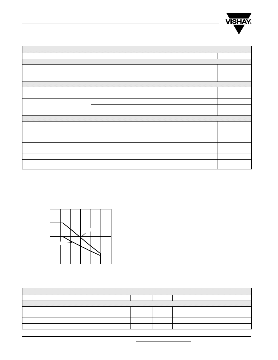
Fig. 1 - Permissible Power Dissipation vs. Ambient Temperature
ABSOLUTE MAXIMUM RATINGS
(1)
PARAMETER
TEST CONDITION
SYMBOL
VALUE
UNIT
INPUT
Reverse voltage
V
R
6
V
Power dissipation
P
diss
mW
Forward current
I
F
60
mA
OUTPUT
Collector emitter voltage
V
CE
55
V
Emitter collector voltage
V
EC
7
V
Collector current
I
C
50
mA
t
p
≤ 1.0 ms
I
C
100
mA
Power dissipation
P
diss
150
mW
COUPLER
Isolation test voltage
between emitter and detector
V
ISO
5300
V
RMS
Isolation resistance
V
IO
= 500 V, T
amb
= 25 °C
R
IO
≥ 10
12
Ω
V
IO
= 500 V, T
amb
= 100 °C
R
IO
≥ 10
11
Ω
Storage temperature range
T
stg
- 55 to + 150
°C
Ambient temperature range
T
amb
- 55 to + 100
°C
Junction temperature
T
j
100
°C
Soldering temperature
(2)
max. 10 s, dip soldering distance
to seating plane
≥ 1.5 mm
T
sld
260
°C
0
50
100
150
200
0
20
40
60
80
100
120
19386
P
- Po
w
er Dissipation (m
W
)
tot
Detector
LED
T
amb
- Ambient Temperature (°C)
ELECTRICAL CHARACTERISTICS
PARAMETER
TEST CONDITION
PART
SYMBOL
MIN.
TYP.
MAX.
UNIT
INPUT
Forward voltage
I
F
= 5 mA
V
F
1.1
1.5
V
Reverse current
V
R
= 6 V
I
R
0.01
10
µA
Capacitance
V
R
= 0 V, f = 1 MHz
C
O
25
pF
Thermal resistance
R
thja
1070
K/W
Document Number: 83673
For technical questions, contact: optocoupler.answers@vishay.com
www.vishay.com
Rev. 1.9, 10-Dec-08
653
SFH618A, SFH6186
Optocoupler, Phototransistor Output,
Low Input Current
Vishay Semiconductors
Note
T
amb
= 25 °C, unless otherwise specified.
Minimum and maximum values are testing requirements. Typical values are characteristics of the device and are the result of engineering
evaluation. Typical values are for information only and are not part of the testing requirements.
OUTPUT
Collector emitter leakage current
V
CE
= 10 V
I
CEO
10
200
nA
Collector emitter capacitance
V
CE
= 5 V, f = 1 MHz
C
CE
7
pF
Thermal resistance
R
thja
500
K/W
COUPLER
Collector emitter saturation voltage
I
C
= 0.32 mA, I
F
= 1 mA
SFH618A-2
V
CEsat
0.25
0.4
V
SFH6186-2
V
CEsat
0.25
0.4
V
I
C
= 0.5 mA, I
F
= 1 mA
SFH618A-3
V
CEsat
0.25
0.4
V
SFH6186-3
V
CEsat
0.25
0.4
V
I
C
= 0.8 mA, I
F
= 1 mA
SFH618A-4
V
CEsat
0.25
0.4
V
SFH6186-4
V
CEsat
0.25
0.4
V
I
C
= 1.25 mA, I
F
= 1 mA
SFH618A-5
V
CEsat
0.25
0.4
V
SFH6186-5
V
CEsat
0.25
0.4
V
Coupling capacitance
C
C
0.25
pF
CURRENT TRANSFER RATIO
PARAMETER
TEST CONDITION
PART
SYMBOL
MIN.
TYP.
MAX.
UNIT
I
C
/I
F
I
F
= 1 mA, V
CE
= 0.5 V
SFH618A-2
CTR
63
125
%
SFH6186-2
CTR
63
125
%
I
F
= 0.5 mA, V
CE
= 1.5 V
SFH618A-2
CTR
32
75
%
SFH6186-2
CTR
32
75
%
I
F
= 1 mA, V
CE
= 0.5 V
SFH618A-3
CTR
100
200
%
SFH6186-3
CTR
100
200
%
I
F
= 0.5 mA, V
CE
= 1.5 V
SFH618A-3
CTR
50
120
%
SFH6186-3
CTR
50
120
%
I
F
= 1 mA, V
CE
= 0.5 V
SFH618A-4
CTR
160
320
%
SFH6186-4
CTR
160
320
%
I
F
= 0.5 mA, V
CE
= 1.5 V
SFH618A-4
CTR
80
200
%
SFH6186-4
CTR
80
200
%
I
F
= 1 mA, V
CE
= 0.5 V
SFH618A-5
CTR
250
500
%
SFH6186-5
CTR
250
500
%
I
F
= 0.5 mA, V
CE
= 1.5 V
SFH618A-5
CTR
125
300
%
SFH6186-5
CTR
125
300
%
SWITCHING CHARACTERISTICS
PARAMETER
TEST CONDITION
SYMBOL
MIN.
TYP.
MAX.
UNIT
Turn on time
V
CC
= 5 V, I
C
= 2 mA, R
L
= 100
Ω
t
on
6
µs
Rise time
V
CC
= 5 V, I
C
= 2 mA, R
L
= 100
Ω
t
r
3.5
µs
Turn off time
V
CC
= 5 V, I
C
= 2 mA, R
L
= 100
Ω
t
off
5.5
µs
Fall time
V
CC
= 5 V, I
C
= 2 mA, R
L
= 100
Ω
t
f
5
µs
ELECTRICAL CHARACTERISTICS
PARAMETER
TEST CONDITION
PART
SYMBOL
MIN.
TYP.
MAX.
UNIT
www.vishay.com
For technical questions, contact: optocoupler.answers@vishay.com
Document Number: 83673
654
Rev. 1.9, 10-Dec-08
SFH618A, SFH6186
Vishay Semiconductors
Optocoupler, Phototransistor Output,
Low Input Current
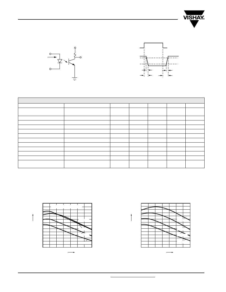
Fig. 2 - Test Circuit
Fig. 3 - Test Circuit and Waveforms
Note
As per IEC 60747-5-2, § 7.4.3.8.1, this optocoupler is suitable for "safe electrical insulation" only within the safety ratings. Compliance with the
safety ratings shall be ensured by means of protective circuits.
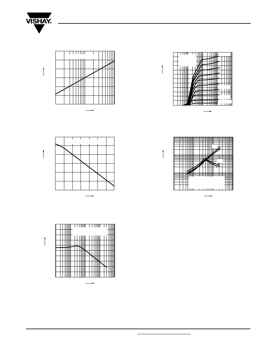
TYPICAL CHARACTERISTICS
T
amb
= 25 °C, unless otherwise specified
Fig. 4 - Current Transfer Ratio (typ.)
Fig. 5 - Current Transfer Ratio (typ.)
isfh618a_10
Input
V
OUT
V
CC
= 5 V
R
L
isfh618a_12
10 %
90 %
Input pulse
Output pulse
t
r
t
on
t
f
t
off
SAFETY AND INSULATION RATINGS
PARAMETER
TEST CONDITION
SYMBOL
MIN.
TYP.
MAX.
UNIT
Climatic classification
(according to IEC 68 part 1)
55/100/21
Comparative tracking index
CTI
175
399
V
IOTM
10000
V
V
IORM
890
V
P
SO
400
mW
I
SI
275
mA
T
SI
175
°C
Creepage distance
standard DIP-4
7
mm
Clearance distance
standard DIP-4
7
mm
Creepage distance
400 mil DIP-4
8
mm
Clearance distance
400 mil DIP-4
8
mm
Insulation thickness,
reinforced rated
per IEC 60950 2.10.5.1
0.4
mm
240
280
%
200
160
- 40 - 20
0
20
40
60
ºC
100
isfh618a_01
T
A
120
80
40
0
CTR
IF = 5mA
IF = 1mA
IF = 2mA
IF = 0.5mA
VCE = 0.5 V, CTR = f (TA)
240
280
%
200
160
- 40 - 20
0
20
40
60
ºC
100
isfh618a_02
T
A
120
80
40
0
CTR
IF = 5mA
IF = 1mA
IF = 2mA
IF = 0.5mA
Document Number: 83673
For technical questions, contact: optocoupler.answers@vishay.com
www.vishay.com
Rev. 1.9, 10-Dec-08
655
SFH618A, SFH6186
Optocoupler, Phototransistor Output,
Low Input Current
Vishay Semiconductors
Fig. 6 - Diode Forward Voltage (typ.)
Fig. 7 - Diode Forward Voltage (typ.)
Fig. 8 - Transistor Capacitance
Fig. 9 - Output Characteristics
Fig. 10 - Switching Times (typ.)
1.15
1.2
V
1.1
1.05
mA
isfh618a_03
I
F
1
0.95
0.9
Vr
TA = 25 ºC, VF = f (IF)
10-1
100
101
1.15
1.2
V
1.1
- 40 - 20
0
20
40
60
ºC
100
isfh618a_04
T
A
1.05
1
0.95
0
VF
IF = 1.0 mA, VF = f (TA)
16
20
pF
12
V
isfh618a_05
V
CE
8
4
0
C
CE
TA = 25 ºC, f = 1.0 MHz
CEE = f (VCE)
10-1
100
101
102
10-2
10
12
mA
8
V
isfh618a_06
V
CE
6
4
2
0
I
CE
TA = 25 ºC,
CE = f
(VCE, IF)
10
-1
10
0
10
1
10
2
10
-2
IF = 5 mA
IF = 2 mA
IF = 1 mA
IF = 0.5 mA
OHOO2119
103
102
101
100
Ω
isfh618a_09
R
L
t
103
104
105
102
μ5
t
F
t off
t
R
t
on
TA = 25 ºC, IF = 1.0 mA,
VCC = 5.0 V, tON, tR,
tOFF, tF, = f (RL)
www.vishay.com
For technical questions, contact: optocoupler.answers@vishay.com
Document Number: 83673
656
Rev. 1.9, 10-Dec-08
SFH618A, SFH6186
Vishay Semiconductors
Optocoupler, Phototransistor Output,
Low Input Current
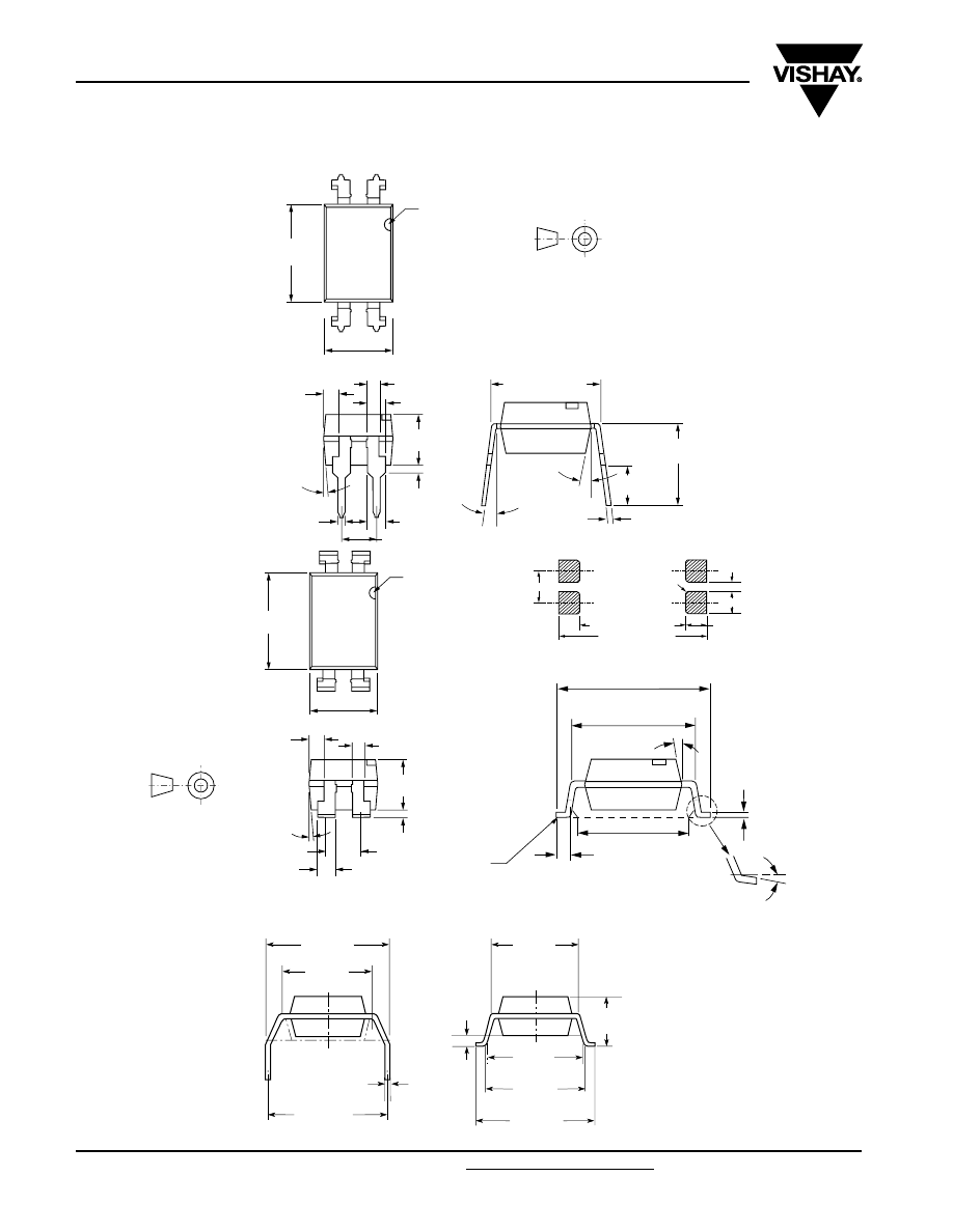
PACKAGE DIMENSIONS in inches (millimeters)
i178027
0.255 (6.48)
0.268 (6.81)
1
2
4
3
0.179 (4.55)
0.190 (4.83)
Pin one ID
0.030 (0.76)
0.045 (1.14)
4°
typ.
0.100 (2.54)
0.130 (3.30)
0.150 (3.81)
0.020 (0.508)
0.035 (0.89)
10°
3° to 9°
0.018 (0.46)
0.022 (0.56)
0.008 (0.20)
0.012 (0.30)
0.031 (0.79) typ.
0.050 (1.27) typ.
0.300 (7.62) typ.
0.110 (2.79)
0.130 (3.30)
0.230 (5.84)
0.250 (6.35)
0.050 (1.27)
ISO method A
i178029
0.255 (6.48)
0.268 (6.81)
3 4
0.179 (4.55)
0.190 (4.83)
Pin one ID
0.030 (0.76)
0.045 (1.14)
4° typ.
1.00 (2.54)
typ.
0.130 (3.30)
0.150 (3.81)
0.0098
(0.249)
0.035 (0.102)
0.020 (0.508)
0.040 (1.02)
0.031 (0.79)
typ.
0.050 (1.27)
typ.
0.010 (0.25)
typ.
10 °
3° to 7°
0.375 (9.52)
0.395 (10.03)
0.296 (7.52)
0.312 (7.90)
0.315 (8.00)
min.
Lead
coplanarity
0.004 max.
SMD
ISO method A
0.100 (2.54)
R 0.010 (0.25)
0.070 (1.78)
0.030 (0.76)
0.315 (8.00) min.
0.060 (1.52)
0.435 (11.05)
0.407 (10.36)
0.391 (9.96)
Optio n 6
min.
0.300 (7.62)
typ.
min.
max.
0.028 (0.7)
Option 7
18450-1
0.307 (7.8)
0.291 (7.4)
0.014 (0.35)
0.010 (0.25)
0.400 (10.16)
0.430 (10.92)
0.180 (4.6)
0.160 (4.1)
0.315 (8.0)
0.331 (8.4)
0.406 (10.3)

Document Number: 83673
For technical questions, contact: optocoupler.answers@vishay.com
www.vishay.com
Rev. 1.9, 10-Dec-08
657
SFH618A, SFH6186
Optocoupler, Phototransistor Output,
Low Input Current
Vishay Semiconductors
OZONE DEPLETING SUBSTANCES POLICY STATEMENT
It is the policy of Vishay Semiconductor GmbH to
1. Meet all present and future national and international statutory requirements.
2. Regularly and continuously improve the performance of our products, processes, distribution and operating systems with
respect to their impact on the health and safety of our employees and the public, as well as their impact on the environment.
It is particular concern to control or eliminate releases of those substances into the atmosphere which are known as ozone
depleting substances (ODSs).
The Montreal Protocol (1987) and its London Amendments (1990) intend to severely restrict the use of ODSs and forbid their use
within the next ten years. Various national and international initiatives are pressing for an earlier ban on these substances.
Vishay Semiconductor GmbH has been able to use its policy of continuous improvements to eliminate the use of ODSs listed in
the following documents.
1. Annex A, B and list of transitional substances of the Montreal Protocol and the London Amendments respectively.
2. Class I and II ozone depleting substances in the Clean Air Act Amendments of 1990 by the Environmental Protection Agency
(EPA) in the USA.
3. Council Decision 88/540/EEC and 91/690/EEC Annex A, B and C (transitional substances) respectively.
Vishay Semiconductor GmbH can certify that our semiconductors are not manufactured with ozone depleting substances and do
not contain such substances.
We reserve the right to make changes to improve technical design
and may do so without further notice.
Parameters can vary in different applications. All operating parameters must be validated for each customer application by the
customer. Should the buyer use Vishay Semiconductors products for any unintended or unauthorized application, the buyer shall
indemnify Vishay Semiconductors against all claims, costs, damages, and expenses, arising out of, directly or indirectly, any
claim of personal damage, injury or death associated with such unintended or unauthorized use.
Vishay Semiconductor GmbH, P.O.B. 3535, D-74025 Heilbronn, Germany

Document Number: 91000
www.vishay.com
Revision: 18-Jul-08
1
Disclaimer
Legal Disclaimer Notice
Vishay
All product specifications and data are subject to change without notice.
Vishay Intertechnology, Inc., its affiliates, agents, and employees, and all persons acting on its or their behalf
(collectively, “Vishay”), disclaim any and all liability for any errors, inaccuracies or incompleteness contained herein
or in any other disclosure relating to any product.
Vishay disclaims any and all liability arising out of the use or application of any product described herein or of any
information provided herein to the maximum extent permitted by law. The product specifications do not expand or
otherwise modify Vishay’s terms and conditions of purchase, including but not limited to the warranty expressed
therein, which apply to these products.
No license, express or implied, by estoppel or otherwise, to any intellectual property rights is granted by this
document or by any conduct of Vishay.
The products shown herein are not designed for use in medical, life-saving, or life-sustaining applications unless
otherwise expressly indicated. Customers using or selling Vishay products not expressly indicated for use in such
applications do so entirely at their own risk and agree to fully indemnify Vishay for any damages arising or resulting
from such use or sale. Please contact authorized Vishay personnel to obtain written terms and conditions regarding
products designed for such applications.
Product names and markings noted herein may be trademarks of their respective owners.
Document Outline
Wyszukiwarka
Podobne podstrony:
więcej podobnych podstron