1N4148.1N4448
Vishay
Semiconductors
1 (4)
Rev. 4, 12-Feb-01
www.vishay.com
Document Number 85521
Fast Switching Diodes
Features
D
Silicon Epitaxial Planar Diodes
D
Electrically equivalent diodes:
1N4148 – 1N914
1N4448 – 1N914B
Applications
Extreme fast switches
94 9367
Order Instruction
Type
Type Differentiation
Ordering Code
Remarks
1N4148
V
= 100 V V @I 10mA = 1 V
1N4148–TAP
Ammopack
1N4148
V
RRM
= 100 V, V
F
@I
F
10mA = 1 V
1N4148–TR
Tape and Reel
1N4448
V
RRM
= 100 V V
F
@I
F
100mA = 1 V
1N4448–TAP
Ammopack
1N4448
V
RRM
= 100 V, V
F
@I
F
100mA = 1 V
1N4448–TR
Tape and Reel
Absolute Maximum Ratings
T
j
= 25
_
C
Parameter
Test Conditions
Type
Symbol
Value
Unit
Repetitive peak reverse voltage
V
RRM
100
V
Reverse voltage
V
R
75
V
Peak forward surge current
t
p
=1
m
s
I
FSM
2
A
Repetitive peak forward current
I
FRM
500
mA
Forward current
I
F
300
mA
Average forward current
V
R
=0
I
FAV
150
mA
Power dissipation
l=4 mm, T
L
=45
°
C
P
V
440
mW
Power dissipation
l=4 mm, T
L
x
25
°
C
P
V
500
mW
Junction temperature
T
j
200
°
C
Storage temperature range
T
stg
–65...+200
°
C
Maximum Thermal Resistance
T
j
= 25
_
C
Parameter
Test Conditions
Symbol
Value
Unit
Junction ambient
l=4 mm, T
L
=constant
R
thJA
350
K/W
1N4148.1N4448
Vishay
Semiconductors
2 (4)
Rev. 4, 12-Feb-01
www.vishay.com
Document Number 85521
Electrical Characteristics
T
j
= 25
_
C
Parameter
Test Conditions
Type
Symbol
Min
Typ
Max
Unit
I
F
=5mA
1N4448
V
F
0.62
0.72
V
Forward voltage
I
F
=10mA
1N4148
V
F
1
V
g
I
F
=100mA
1N4448
V
F
1
V
V
R
=20 V
I
R
25
nA
Reverse current
V
R
=20 V, T
j
=150
°
C
I
R
50
m
A
V
R
=75 V
I
R
5
m
A
Breakdown voltage
I
R
=100
m
A, t
p
/T=0.01,
t
p
=0.3ms
V
(BR)
100
V
Diode capacitance
V
R
=0, f=1MHz, V
HF
=50mV
C
D
4
pF
Rectification efficiency
V
HF
=2V, f=100MHz
h
r
45
%
I
F
=I
R
=10mA, i
R
=1mA
t
rr
8
ns
Reverse recovery time
I
F
=10mA, V
R
=6V, i
R
=0.1xI
R
,
R
L
=100
W
t
rr
4
ns
Characteristics (T
j
= 25
_
C unless otherwise specified)
–30
0
30
60
90
0
0.2
0.4
0.6
0.8
1.2
V
– Forward
V
oltage (
V
)
F
T
j
– Junction Temperature (
°
C )
120
94 9169
1.0
I
F
= 100 mA
10 mA
1 mA
0.1 mA
Figure 1. Forward Voltage vs. Junction Temperature
0
0.4
0.8
1.2
1.6
0.1
1
10
100
1000
I – Forward Current ( mA
)
F
V
F
– Forward Voltage ( V )
2.0
94 9170
1 N 4148
Scattering Limit
T
j
= 25
°
C
Figure 2. Forward Current vs. Forward Voltage
1N4148.1N4448
Vishay
Semiconductors
3 (4)
Rev. 4, 12-Feb-01
www.vishay.com
Document Number 85521
0
0.4
0.8
1.2
1.6
0.1
1
10
100
1000
I – Forward Current ( mA
)
F
V
F
– Forward Voltage ( V )
2.0
94 9171
1 N 4448
Scattering Limit
T
j
= 25
°
C
Figure 3. Forward Current vs. Forward Voltage
1
10
1
10
100
1000
I – Reverse Current ( nA
)
R
V
R
– Reverse Voltage ( V )
100
94 9098
Scattering Limit
T
j
= 25
°
C
Figure 4. Reverse Current vs. Reverse Voltage
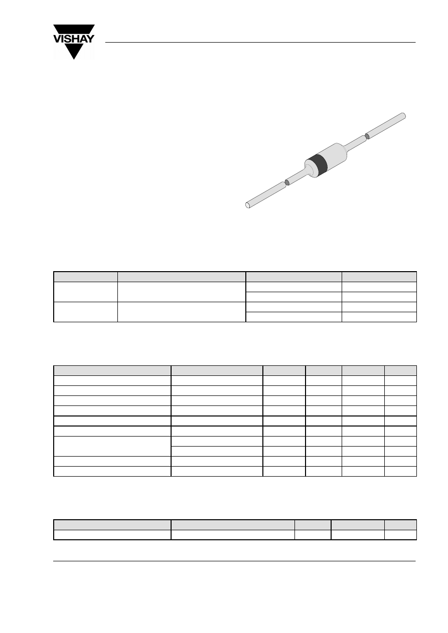
Dimensions in mm
Cathode Identification
∅
1.7 max.
∅
0.55 max.
3.9 max.
26 min.
technical drawings
according to DIN
specifications
94 9366
Standard Glass Case
54 A 2 DIN 41880
JEDEC DO 35
Weight max. 0.3 g
26 min.

1N4148.1N4448
Vishay
Semiconductors
4 (4)
Rev. 4, 12-Feb-01
www.vishay.com
Document Number 85521
Ozone Depleting Substances Policy Statement
It is the policy of Vishay Semiconductor GmbH to
1. Meet all present and future national and international statutory requirements.
2. Regularly and continuously improve the performance of our products, processes, distribution and operating
systems with respect to their impact on the health and safety of our employees and the public, as well as their
impact on the environment.
It is particular concern to control or eliminate releases of those substances into the atmosphere which are known as
ozone depleting substances ( ODSs ).
The Montreal Protocol ( 1987 ) and its London Amendments ( 1990 ) intend to severely restrict the use of ODSs and
forbid their use within the next ten years. Various national and international initiatives are pressing for an earlier ban
on these substances.
Vishay Semiconductor GmbH has been able to use its policy of continuous improvements to eliminate the use of
ODSs listed in the following documents.
1. Annex A, B and list of transitional substances of the Montreal Protocol and the London Amendments respectively
2 . Class I and II ozone depleting substances in the Clean Air Act Amendments of 1990 by the Environmental
Protection Agency ( EPA ) in the USA
3. Council Decision 88/540/EEC and 91/690/EEC Annex A, B and C ( transitional substances ) respectively.
Vishay Semiconductor GmbH can certify that our semiconductors are not manufactured with ozone depleting
substances and do not contain such substances.
We reserve the right to make changes to improve technical design and may do so without further notice.
Parameters can vary in different applications. All operating parameters must be validated for each customer application
by the customer. Should the buyer use Vishay-
Semiconductors
products for any unintended or unauthorized application, the
buyer shall indemnify Vishay-Telefunken against all claims, costs, damages, and expenses, arising out of, directly or
indirectly, any claim of personal damage, injury or death associated with such unintended or unauthorized use.
Vishay Semiconductor GmbH, P.O.B. 3535, D-74025 Heilbronn, Germany
Telephone: 49 ( 0 ) 7131 67 2831, Fax number: 49 ( 0 ) 7131 67 2423

This datasheet has been download from:
Datasheets for electronics components.
Wyszukiwarka
Podobne podstrony:
300 mA dioda przełączająca-impulsowa 1N4148 na 100 V
rozwiazany test z poligrafii ale odp prawidlowe nie sa na 100 , Poligrafia
Ark.egz.odporność, Matura na 100%
więcej podobnych podstron