The Ultimate
Data Collection
ave you ever thought about the vast amounts of
data the human brain collects and processes each
day? The raw data coming from your eyes alone would
overwhelm even the fastest computer available today with
gigabytes of storage. Consider the most mundane daily tasks of recognizing
objects on a table, listening to and understanding the spoken word (or even
simple telephone call progress tones), using just the right amount of
pressure to grasp a delicate object without crushing it, or picking out the
subtle aroma of burning potpourri from a roomful of other smells.
Given the wonders of the human body, we have a remarkable amount
of work left to do to even approximate a single human sensory processing
system. Going back to my sight example, think about the work involved in
trying to get a computer with an attached video camera to simply recognize
that a human face
is somewhere in its field of view. I contrast that
with being able to stare at my newborn daughter’s face and compare her
features with those of her older sister. The lips are the same, but the nose
isn’t quite as upturned and the shape of her head is different. The person
who can make a computer do that will be very rich indeed.
Returning to the world of the practical, our first data acquisition feature
article this month considers the ubiquitous laboratory strip-chart recorder.
While simple in concept, it can be expensive. By applying some much
cheaper off-the-shelf hardware and some code, we can make a dot-matrix
printer do much of the same work.
Next, for those who want to collect data so fast it taxes the capabilities
of today’s best desktop machine, we present
a
1
converter board for the ISA bus. Along with covering the details about the
board itself, we also show how the
board was applied to calibrating
some seismic sensors.
Finally, following up on an article we carried a few months ago on
ownership of work, we look at the current debate raging over copyrights and
patents for software.
The legal world has a lot of catching up to do.
In our columns, Ed starts a series of articles exploring the somewhat
scary world of protected mode programming; Jeff checks out the current
state of low-cost voice recognition hardware (it’s still not even close to
human standards); Tom surveys the current crop of sensors and their slow
migration into the digital realm; and John starts experimenting with the
Dallas Semiconductor
microprocessor that can speed up any
8031 system by simply replacing the processor.
2
Issue August 1994
The Computer Applications Journal
CIRCUIT CELLAR
THECOMPUTER
APPLICATIONS
JOURNAL
FOUNDER/EDITORIAL DIRECTOR
Steve Ciarcia
EDITOR-IN-CHIEF
Ken Davidson
TECHNICAL EDITOR
Janice Marinelli
ENGINEERING STAFF
Jeff Bachiochi Ed Nisley
WEST COAST EDITOR
Tom Cantrell
CONTRIBUTING EDITORS
John Dybowski Russ Reiss
NEW PRODUCTS EDITOR
Hatv Weiner
ART DIRECTOR
Lisa Ferry
GRAPHIC ARTIST
Joseph Quinlan
PUBLISHER
Daniel Rodrigues
PUBLISHER’S ASSISTANT
Sue Hodge
CIRCULATION COORDINATOR
Rose
CIRCULATION ASSISTANT
Barbara
CIRCULATION CONSULTANT
Gregory Spitzfaden
BUSINESS MANAGER
Jeannette Walters
ADVERTISING COORDINATOR
Dan Gorsky
CIRCUIT CELLAR INK, THE COMPUTER
JOURNAL (ISSN
is
monthly by
Cellar Incorporated. 4 Park Street.
20, Vernon, CT 06066 (203)
Second
class
One-year
rate
and
CONTRIBUTORS:
Jon Elson
Tim
Frank Kuechmann
Kaskinen
$49.95. All
orders payable US
funds only, via
postal money order
check drawn on U.S. bank.
orders
and
related questions The Computer
Journal Subscriptions, P.O. Box 7694,
NJ 06077 call (609)
POSTMASTER, Please send address changes to The
Computer
Journal,
Dept., P 0
Box 7694,
NJ 06077.
Cover Illustration by Bob Schuchman
PRINTED IN THE UNITED STATES
ASSOCIATES
NATIONAL ADVERTISING REPRESENTATIVES
NORTHEAST
SOUTHEAST
Debra Andersen
Collins
WEST COAST
Barbara Jones
(617)
Fax:
(617) 769-8982
MID-ATLANTIC
Barbara Best
(305) 966-3939
Fax: (305) 985-8457
MIDWEST
Nanette Traetow
Shelley
(714) 540-3554
Fax: (714)
(908) 741-7744
Fax: (908) 741-6823
(708) 789-3080
Fax: (708) 789-3082
bits,
1 stop bit,
9600 bps Courier
(203)
All programs and
Cellar
been carefully
to ensure
of
programs schematics
the consequences of any such errors. Furthermore, because of possible
the
and
of
and
reader-assembled projects.
Cellar INK
any
the safe and proper function of reader-assembled projects based upon from
plans, descriptions.
Circuit
INK.
contents
1994 by
Cellar Incorporated. All
reserved.
of
in whole pall
consent from Circuit Cellar Inc.
1 4
The Two-channel Printer Recorder/Replace that Expensive
Strip-chart Recorder with a Dot-matrix Printer
by Brian
2 8
Get Precise, with the
A/D
Converter/Collect Lots
of Precise Data with this 16-bit,
ADC
by Conrad Hubert
3 8
Calibrating Seismic Velocity Transducers with
by Chris Peoples
4 4
Patents and Copyrights for Protecting Software/Recent
Progress in Finding the Proper Balance
by Barry Rein, Esq.
5 2
q
Firmware Furnace
Journey to the Protected Land:
Segments All the Way Down
Ed Nisley
6 0
q
From the Bench
Ta( 1) king Control
Bachiochi
6 8
q
Silicon Update
In the Realm of the Sensors
Tom Can trell
7 4
q
Embedded Techniques
Speed Demon in 803 l’s Clothing/Exploring
the
Processor
Dybowski
New Product News
edited by Harv Weiner
Excerpts from
the Circuit Cellar BBS
conducted by
Ken Davidson
Steve’s Own INK
Steve Ciarcia
Time to Move On
Advertiser’s Index
The Computer Applications Journal
Issue
August 1994
3
So Let’s Hear it for the Environment
I have been following Circuit Cellar INK since its
appearance. I have never seen articles related to the
environment. I would like to know, for example, how
I
can use the wind and the sun to provide electricity in my
home? The design of a control system to store the energy
and monitor power consumption would be interesting.
Everybody can benefit from using conventional
forms of energy. Some areas are particularly suitable for
using the wind and/or solar energy. In the Mediterranean
area, for instance, there is a huge installation of solar
panels used to provide hot water. Maybe these panels
could be used in an additional way. There are ways
(special heat pumps) to use underground water to heat a
house in the winter or air condition it in the summer.
There is air and water pollution in almost every city,
and
I
believe it would be interesting to learn how one
can measure the mass of the various gases (CO,
NO, etc.). I’d also like to be able to measure the pollu-
tion in the water resources.
Please include articles that will help me do my part
in saving the environment.
Yannis Roussias
Athens, Greece
LAN/WAN Chip Set: One Chip Only Please
I
have been a subscriber since issue
that issue
was an article discussing the ISDN BRI chip set that
AT&T Microelectronics had developed. Since then, I
have seen many articles on
X-10 and now, in
issue
I have enjoyed reading them and
like the detail you provided. I have an interest that you
could satisfy with articles similar to the AT&T article.
I have developed a great deal of appreciation for the
complexity of the IS0
network model. ISDN, X-25,
LAN, and WAN protocols are all defined as the lower
part of it with the
interface of each being identical. I
believe that, with single-chip implementations of
layers, l-3 should now be possible or at least
more complete than the 1991 AT&T chip set, which
didn’t have B channel multiplexing, security, account-
ing, or control management. I believe Rockwell,
Seimens, Northern Telecom BNR, and AT&T are all
working on this. Could you check with them to see if
one of them would consider writing an article for your
magazine on their work?
Along these lines, I also would like to see X-25 over
serial/parallel cabling discussed, preferably with
chip implementation. LAN and WAN single chips are
also possible, but most that I have seen have truncated
their protocol support with the Microsoft-defined NDIS
drive interface, instead of the ANSI/ISO-defined inter-
face. A single-chip implementation of LAN and WAN
protocols to the
level
interface (sans
routing) would be an interesting series of articles.
I say this as the IS0 has finally finished the manage-
ment functions definitions in 1992. Thus, the chips now
coming out will or should have complete support for all
lower-level operations.
William L.
Garland, TX
New Address
The Fomebords Co. was listed in the source section
at the end of the “Prototyping-Beyond Electronics and
Software” article in the June 1994 issue. They have since
changed their name and address. Contact them at
Superior Fomebords Corp.
1040 N. Halsted St.
Chicago, IL 60622
(312)
(800) 362-6267
Contacting Circuit Cellar
We at the
Journal encourage
communication between our readers and our staff, have made
every effort to make contacting us easy. We prefer electronic
communications, but feel free to use any of the following:
Mail:
Letters to the Editor may be sent to: Editor, The Computer
Applications Journal, 4 Park St., Vernon, CT 06066.
Phone:
Direct all subscription inquiries to (609) 786-0409.
Contact our editorial offices at (203) 8752199.
Fax:
All faxes may be sent to (203)
BBS: All of our editors and regular authors frequent the Circuit
Cellar BBS and are available to answer questions. Call
(203) 871-l 988 with your modem (300-l
bps,
Internet: Electronic mail
may also be sent to our editors and
regular authors via the Internet. To determine a particular
person’s Internet address, use their name as it appears in
the masthead or by-line, insert a period between their first
and last names, and append
to the end.
For example, to send Internet E mail to Jeff Bachiochi,
address it to
For more
information, send E mail to
6
Issue
August 1994
The Computer Applications Journal
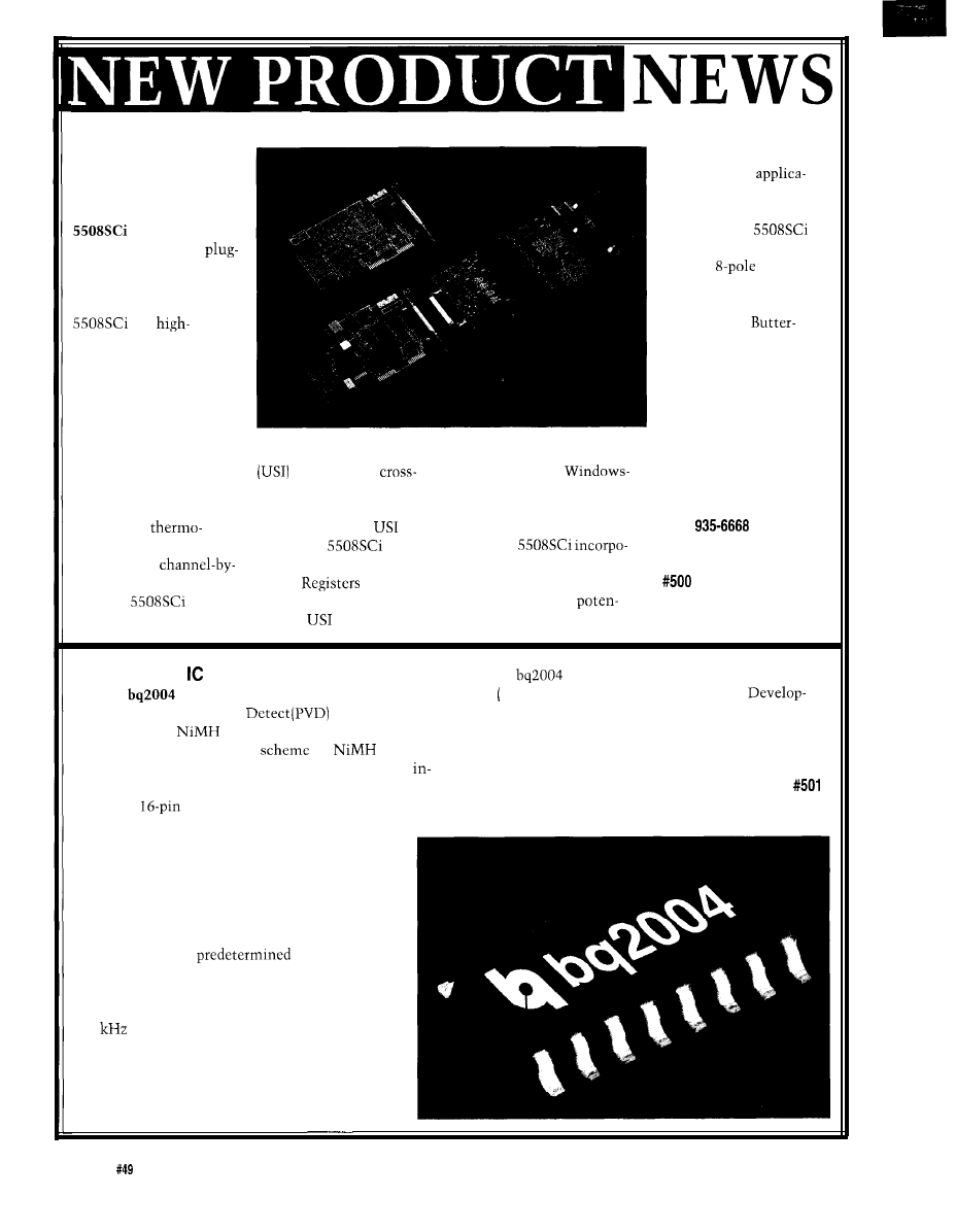
Edited by Harv Weiner
ADC BOARD FOR
from entering the host
THERMOCOUPLE
computer. For
DATA ACQUISITION
tions that have the
The
Direct Connect
potential for signal alias
from ADAC
problems, the
Corp. is the first PC
can be ordered with
in board designed for
integral
antialias
industrial thermocouple
filtering. Available on a
data acquisition. The
per-channel basis as
is a
either Bessel,
performance A/D
worth, or Elliptical
converter board that
filtering; the option
includes a detachable
eliminates the need for
screw-terminal panel
costly front-end filter
which provides 1500-V
systems. Prices start at
isolation. The board
$695.
contains integral signal
Universal Software Interface
compatibility with virtually
conditioning to accept
to allow true
every DOS- and
ADAC Corp.
thermocouple inputs
compatibility between
based data acquisition and
70 Tower Off ice Park
directly. In addition, the
software and hardware from
control software package
Woburn, MA 01801
unit allows
different vendors.
available.
(617)
couple type to be user
allows the
to
The
Fax: (617) 938-6553
selected on a
match the Control and
rates isolation located at the
channel basis.
Status
of other
screw terminations outside
The
manufacturer’s plug-in
the PC to prevent
features a unique
boards.
also provides
tially devastating voltages
FAST CHARGE
The
sells for $5.44 (16-pin narrow DIP) and
The
Fast Charge IC
from Benchmarq
$5.83 16-pin narrow SOIC) in I k quantities.
incorporates Peak Voltage
fast charge
ment systems are also available.
termination for
batteries. PVD is the recom-
mended voltage termination
for
from
Benchmarq Microelectronics, Inc.
some battery manufacturers. The bq2004 is ideal for
2611
Westgrove Dr., Ste. 109
l
Carrollton, TX 75006
system charging with a simple-to-use power-down mode
(214) 407-0011
l
Fax: (214) 407-9845
and small
SOIC package.
The bq2004 terminates charge based on
negative delta voltage detection and on tempera-
ture-slope sensing. This involves calculating the
slope of the battery temperature curve using the
rapid temperature increase associated with fully
charged batteries. This technique provides charge
termination quickly when the rate of temperature
increase is outside
limits. Fail-safe
terminations include maximum temperature,
charge time, and battery voltage.
The bq2004 also offers modulated output to
300
for switched-mode current regulation,
LED outputs to display battery and charge status,
low-power standby mode, battery temperature and
voltage qualification before fast charge, and pulse
trickle and “top-off” charge control.
8
Issue
August 1994
The Computer Applications Journal
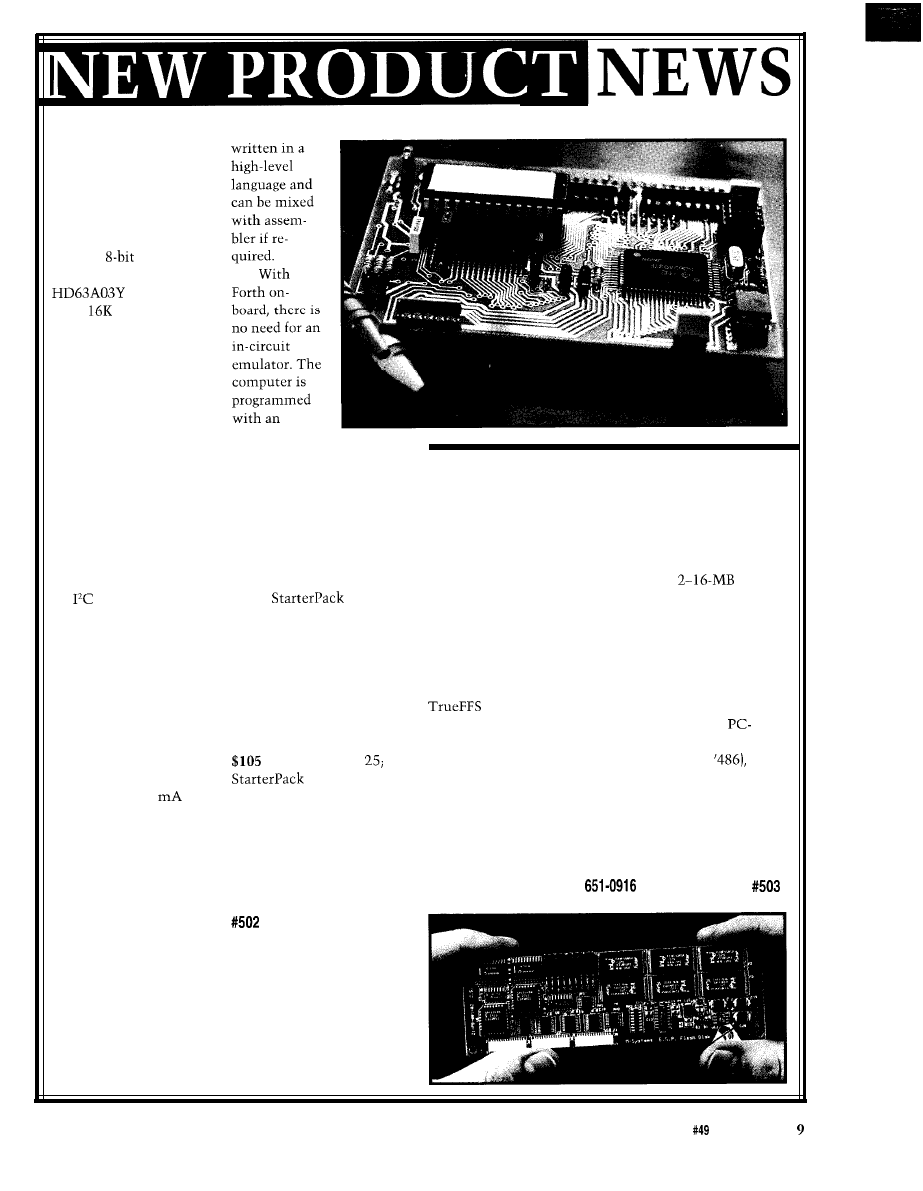
LOW-COST FORTH
COMPUTER
The TDS9092, a
CMOS single-board Forth
computer/controller, is
available from the Saelig
Co. The
computer
features the Hitachi
microproces-
sor, a
Forth language
kernel, and built-in
symbolic assembler.
Generated code can be
stored in either nonvola-
tile RAM or EPROM on-
board. Typical uses for
the unit include ma-
chine-tool control,
instrumentation, data
logging, flow control, and
measurement
The TDS9092
features 35 I/O lines, two
RS-232 serial ports, a
watchdog timer, a driver
for
serial peripherals,
and two timers. Memory
included on the chip
includes 16 KB of RAM
for data collection
applications arrays and
variables, 29 KB user
application space, and
256 bytes nonvolatile
EEPROM. The 4” x 3”
board runs from very
low power (3-15
at
6-16 V) and features a
battery-low output,
touch switch turn-on,
and an on-board regula-
tor.
ordinary PC,
building up program
segments as needed. A
defined assembler routine
can be tested immediately
without any downloading
step. The interactive
debugging of assembler is
very powerful.
A
has
everything needed for fast
instrumentation control. It
includes an improved,
comprehensive, ready-made
software library from which
to mix-and-match subrou-
tines.
The TDS9092 sells for
in quantities of
the
sells for $225.
The Saelig Company
1193 Moseley Rd.
Victor, NY 14564
(716) 425-3753
Fax: (716) 425-3835
FLASH DISK
A line of Flash disk products in the E.S.P. form
factor has been announced by Dovatron. The use of
solid-state disk technology allows system integrators to
greatly reduce power and space while eliminating the
need for rotating media.
The
E.S.P. Flash disk
is available in
capacities, and up to four modules can be added to a
single E.S.P. system. Flash technology allows almost
instant read/write access and requires no power to retain
data when idle. There is an optional boot ROM feature
allowing the system to boot directly from the flash card.
All E.S.P. Flash modules are shipped with M-Systems’s
Flash file utilities software.
E.S.P. (Extremely Small Package) is a 100%
compatible product in a small, low-power form factor.
The product line offers processors (‘286, ‘386,
power supplies, and a variety of I/O functions. All E.S.P.
modules are 1.7” x 5.2” and conform to the ISA electrical
standard.
Dovatron International
1198 Boston Ave.
l
Longmont, CO 80501
(303) 772-5933
l
Fax: (303)
The interactive Forth
specially written for the
board gives easy access to
all its features and allows
software to be quickly
written. The Forth
includes LCD and
keyboard drivers together
with many other utili-
ties. Programs are
The Computer Applications Journal
Issue
August 1994
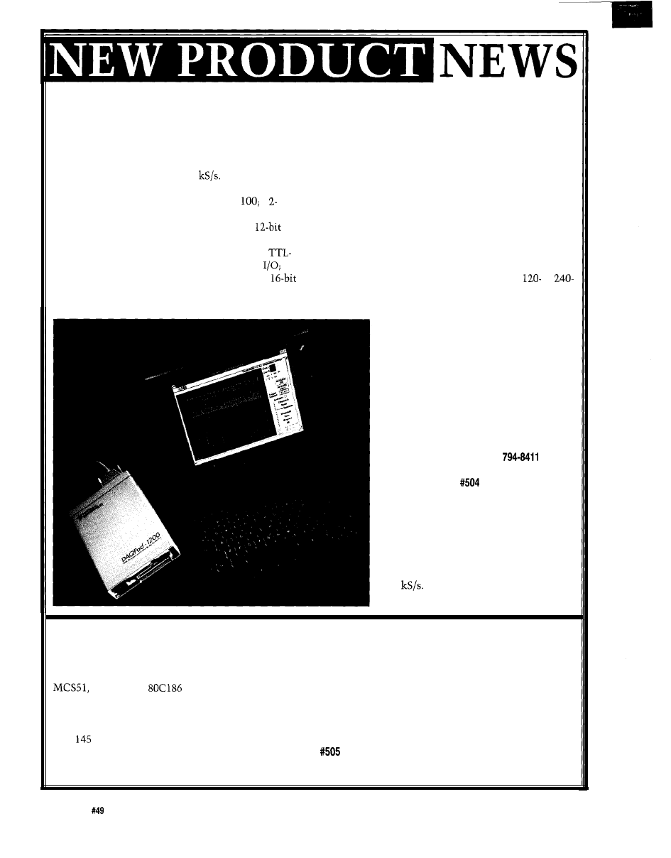
DATA ACQUISITION
BOX
National Instru-
ments has announced a
compact, high-perfor-
mance, external data
acquisition box. Compat-
ible with any PC that has
a parallel printer port,
the DAQPad-1200 is
ideal for PC-based data
acquisition involving
laptop and notebook PCs,
or PCs with the available
slots filled.
The DAQPad- 1200 has
a 12-bit A/D converter that
can digitize from eight
single-ended or four differ-
ential inputs at rates up to
100
It features pro-
grammable gains of 1, 2, 5,
10, 20, 50, or
a
kilosample first-in/first-out
ADC buffer; two
D/A
converters with voltage
outputs; 24 lines of
compatible digital
and
three user-available
counter/timer channels.
The DAQPad- 1200 is
fully software calibrated and
software configurable, with
no jumpers or trimpots. It
can sample in a variety of
modes, including externally
timed acquisition, external
trigger with pre- and
posttrigger mode, and
interval scanning. With
interval scanning, the
DAQPad- 1200 scans all
selected input channels at
one rate, then delays a
programmed interval before
repeating the
scan.
The
DAQPad- 1200
is compatible
with the IEEE
1284 En-
hanced
Parallel Port
(EPP) standard
and works
with two
types of ports:
standard
Centronics
(unidirec-
tional) and the
fast EPP ports.
In EPP mode,
data is
transferred at
rates up to
100
The
DAQPad- 1200
features a second parallel
port connector so users
can simultaneously
connect the unit to a PC
and printer.
Software for the unit
includes NI-DAQ, the
company’s library of
DAQ functions for DOS,
Windows, and Windows
NT applications. The
DAQPad- 1200 includes
an AC adapter to supply
power from a
or
VAC wall outlet. An
optional battery pack
with charger will power
the unit for 9-12 hours.
The DAQPad- 1200
and AC adapter sell for
$995. The battery pack
sells for $295.
National Instruments
6504 Bridge Point Pkwy.
Austin, TX 78730-5039
(512) 794-0100
Fax: (512)
DEVELOPMENT TOOLS HANDBOOK
Intel Corporation has announced the availability of
the Second Edition of the MW Media Development
Tools Handbook,
listing support solutions for the Intel
MCS96, and
architectures.
Created to assist embedded system designers, the
Development Tools Handbook features design support
products and services from 62 companies. It contains
over
pages of information on microcontrollers and
peripheral components, compilers and assemblers,
debuggers, emulators, simulators, analyzers, program-
mers, design services, training, and accessories. Each
page is a complete data sheet detailing each product with
descriptions, features, specifications, contacts, and
ordering information. This edition also contains a
tutorial on “Understanding the Development Cycle” by
Steven McIntyre, an Intel applications manager.
To obtain a free copy of the book, call the Intel
Literature Center at (800) 548-4725.
10
Issue
August 1994
The Computer Applications Journal
CRYPTOGRAPHIC
installation process per-
INSTALLER
formed. After payment
has released new
arrangements, software
versions of Instalit, a
vendors can provide an
cryptographic installer
appropriate key allowing
incorporating public and
product installation. With
private key and RC4
these techniques, customers
encryption. Available in
can purchase new product
14 national languages,
increments at a later date or
Instalit/Crypto is
after trying a demo version.
designed for developers
Instalit/Crypto is a
wanting to lock products
complete product release
on diskettes or CD-ROM.
system. The package
Developers and data
incorporates data compres-
distributors can encrypt
sion, patching, program-
product or data files as
mable automatic release
they are compressed for
production, scriptable
distribution using keys of
compressed library builds,
any length. Distributions
and diskette duplication
can be built so that, even
technology. Versions are
on identical CD-ROMs
available for DOS,
or diskettes, a unique key
Microsoft Windows, or
is needed for each
Windows NT.
A communicating
remote installer version,
called
can install
or intelligently update a
product from a local
computer to a remote
computer via ZMODEM
exactly as though a diskette
set had been sent to the
remote site. Key exchange
can be handled in a com-
pletely automatic fashion.
The software can operate in
unattended mode and can
also be used for directory
synchronization, hardware
and software inventory,
backup, and general scripted
utility functions at remote
sites. Besides remote
installation, the product can
be used for routine cus-
tomer check-in for potential
update purchase with
immediate direct
installation.
Prices start at $299
for Instalit and $349 for
No royalties
apply. Demos are
available on
BBS.
HPI
917C Willowbrook Dr.
Huntsville, AL 35802
(205) 880-8782
Fax: (205) 880-8705
BBS: (205)
l
Easv to use software,
help,
full
editor
l
Made in USA
Year Warranty
l
Technical Support by phone
l
30 day Money Back Guarantee
FREE software upgrades available BBS
Demo SW BBS
(PBlOOEMO.EXE)
2716 8 megabit, 16 bit 27210-27240,
Flash
(EMP-20 only))
Micros
GAL, PLD from NS.
(EMP-20
Orange Grove Ave.
Sacramento, CA 95841
(Monday-Friday. 8 am-5 pm PST)
C.O.D.
FAX (916)
T
E
C
H
N
O
L
O
G
Y
The
Solution
8051.
c o m p a t i b l e
A full range of other processors
s u p p o r t e d
Up 2 5 0 n o d e s
16 Bit CRC
checking with
s e q u e n c e n u m b e r s
Complete
i n c l u d e d
The Computer Applications Journal
issue
August 1994
11
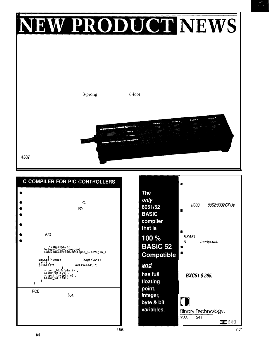
X-10 POWER STRIP
PCS
has provided a solution for the need to plug more than one X-lo-type module into a standard wall outlet.
The Multimodule is the equivalent of four X-IO-compatible modules packaged in a power-strip enclosure.
Multimodule is available in three versions: a four-outlet lamp module, a four-outlet appliance module, and a
combination lamp/appliance module. The lamp version allows the user to safely control any combination of lights
up to 1200 W from any combination of the four outlets. The appliance Multimodule can control any combination of
appliance loads up to 15 amps. Every Multimodule is fully protected by a resettable circuit breaker. Each outlet can
handle the full load, so every individual outlet is completely protected.
The Multimodule features four consecutive addresses and is compatible with all X-10 commands. The 10.5” x
1.7” x 2.6” unit includes standard
receptacles and a
power cord. Advanced features are available to
allow custom user configuration of various options, such as enable/disable of dimming, remote On activation by load
power switch, lamp flashing, and noncontiguous outlet addressing. The lamp module allows outputs to brighten
from off without coming to full On first; preset dim and All Lights Off commands; and retention of the current dim
level when outlet is turned off or when power fails.
Powerline Control Systems
9031 Rathburn Ave.
Northridge, CA 91325
(818) 701-9831
Fax: (818) 701-l 506
Integrated software development environment including an
editor with interactive error detection/correction.
Access to all hardware features from
Includes libraries for RS232 serial
and precision delays.
Efficient function invocation mechanism allowing call trees
deeper than the hardware stack.
Special built-in features such as bit variables optimized to
take advantage of unique hardware capabilities.
Interrupt and
built-in functions for the C71.
Easy to use high level constructs:
#include
# u s e
R u s e
main 0
any key to
khz signal
;
while (TRUE)
compiler
$99 (all 5x chips)
PCM compiler
$99
‘71, ‘84 chips)
Pre-paid shipping $5
COD shipping
$10
CCS, PO Box
11191,
Milwaukee WI
53211
414-78 l-2794 x30
Memory mapped variables
n
In-line assembly language
option
n
Compile time switch to select
805
1 or
Compatible with any RAM
or ROM memory mapping
n
Runs
up
to 50 times faster than
the MCS BASIC-52 interpreter.
Includes Binary Technology’s
cross-assembler
hex file
Extensive documentation
Tutorial included
n
Runs on IBM-PC/XT or
compa tibile
n
Compatible with all 8051 variants
n
508-369-9556
FAX 508-369-9549
Inc.
Box
l
Carlisle, MA 01741
12
Issue
August
1994
The Computer Applications Journal
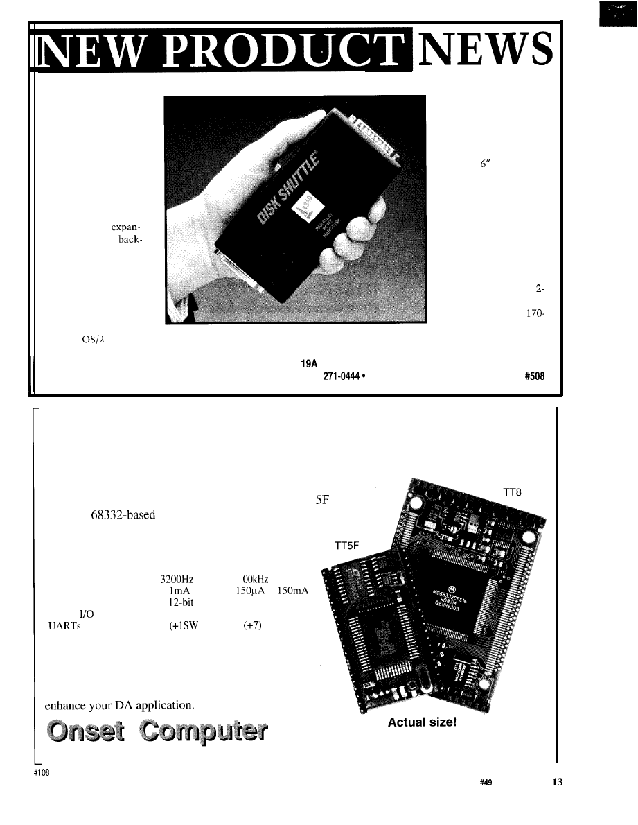
PARALLEL PORT
Disk Shuttle
HARD DISK
features an average
Disk Shuttle is a
access time of 8-12 ms
fast, reliable way to
and a data transfer rate of
increase the hard disk
6 MB/s. The unit
drive storage capacity of
measures x 3” x 1” and
a PC. The palm-sized
weighs 12.5 ounces. The
unit features data storage
Mean Time Between
capacities of 170 MB, 260
Failures (MTBF) is
MB, and 344 MB, and is
300,000 hours.
ideal for storage
Disk Shuttle is
sion, file transfer,
offered as a complete kit.
ups, and PC installations.
It comes in a carrying
Disk Shuttle features
case and includes power
a 2.5” form factor hard
and data cables, driver
disk that installs in
software, manual, and
seconds on any parallel
year warranty. Prices
printer port without
start at $459 for the
additional hardware for
MB model.
DOS and
systems. The printer can be plugged into
the other end of the Disk Shuttle for transparent use. No
Computer Connections America
CONFIG.SYS changes or controller cards are needed and
Crosby Dr.
l
Bedford, MA 01730
software is provided to complete the installation.
(617)
Fax: (617) 271-0873
Powerful, Portable Data Logging Made Easy
If you need a data logger/controller engine with the processing
power and small size to handle the most challenging embedded or
remote data acquisition task, there is an Onset Tattletale@ designed
especially for the job. From the tiny, 8-channel Model
to the
powerful
Model 8, Tattletale loggers offer
unparalleled performance for the price.
Tattletale@ Model
SF
8
Price (unit)
$395
$495
Max sampling rate
1
Min/max current
3.
to 30mA
to
Analog channels
8
8 12-bit
Digital
lines
14
25
1
)
2
Programming Language
BASIC
C, BASIC
Other Tattletale models offer such features as hard disk
storage, LCD displays and cases for hand-held applica-
tions. Call Onset today to discuss how a Tattletale can
PO Box 3450, 536 MacArthur Blvd
l
Pocasset, MA 02559
l
Tel 508-563-9000, Fax 508-563-9477
The Computer Applications Journal
Issue
August 1994
A Two-channel Printer
Recorder
Get Precise, with the
A/D Converter
Calibrating Seismic
Velocity Transducers
with
Copyrights and Patents
for Protecting Software
Printer
Brian Millier
Replace that Expensive
chart Recorder with a
matrix Printer
ne of the
byproducts of the
with the personal computer market is
the availability of many useful devices
that can be obtained “dirt cheap.” This
occurs when some new technology
makes a particular product less
attractive than it was when the
manufacturer ordered all the parts
needed to make thousands or more of
these widgets. Working in a university
chemistry department, often take
advantage of this situation to design
instruments using such inexpensive
components and assemblies.
While research and teaching labs
have embraced computers and modern
data acquisition systems with open
arms, there still exists a substantial
need for the trusty old strip-chart
recorder. The cost of a two-channel
recorder still exceeds $1000 in most
cases. A dot matrix printer, on the
other hand, fighting off low-cost laser
and inkjet printers, can currently be
purchased for well under $200. Add a
microcontroller with A/D conversion,
a large (and cheap) LCD display, and
you have the makings of an inexpen-
sive two-channel strip-chart recorder
with some added advantages thrown
14
Issue
August 1994
The Computer Applications Journal
Channel 1
TMS370
Board
16 Key Pad
I
-
001)
Gnd
VCC
G n d
Channel 2
I
16
DIP
P r i n t e r
NEUTRAL
Parallel
Power
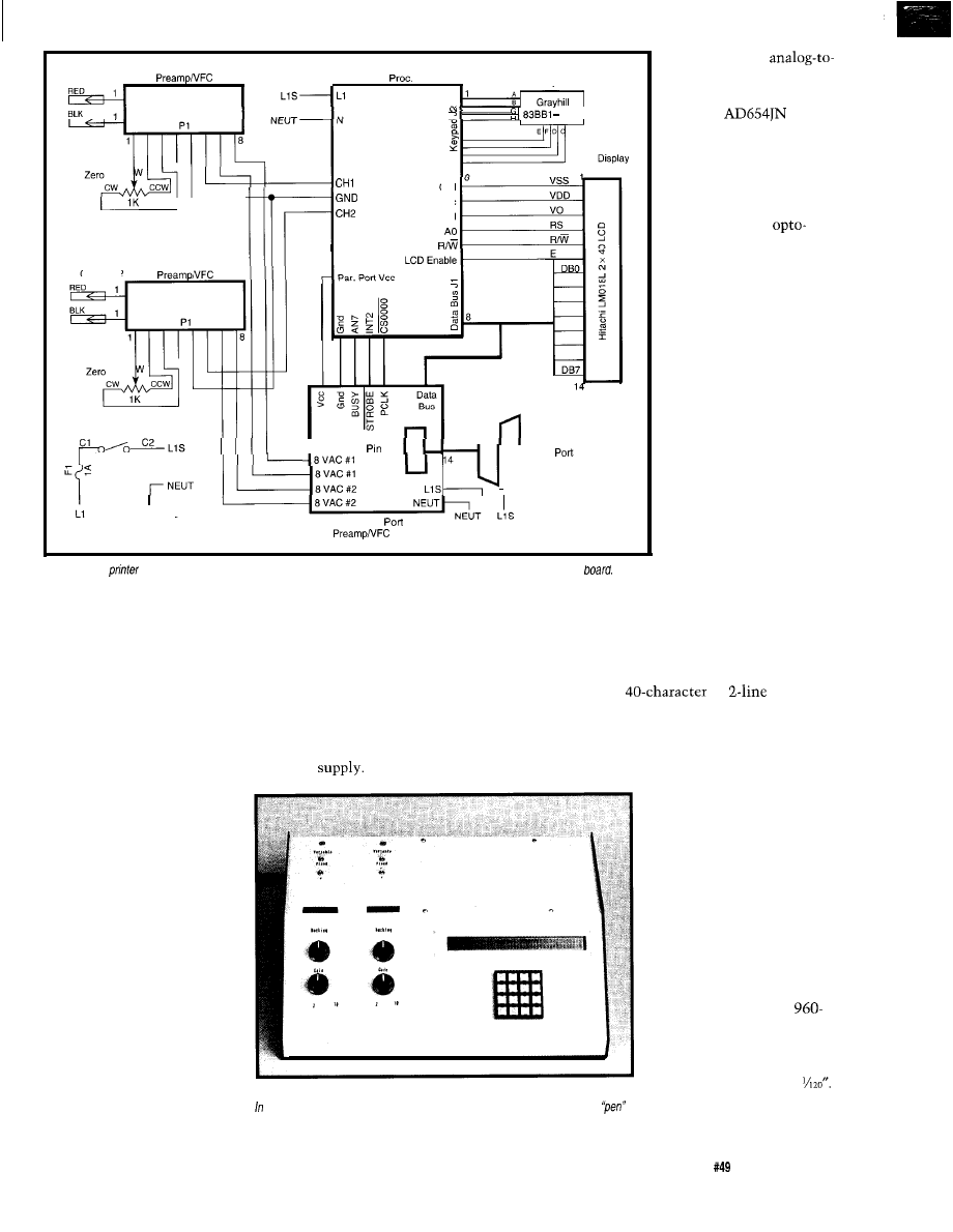
Figure l--The
recorder is built in modules so different front ends
may
be connected to the same core
processor
in. Printer paper is much cheaper than
recorder paper, and this recorder will
print out pertinent information such
as the date, chart speed, and so forth at
the end of the run. Due to the print
speed limitations of the dot matrix
printer, though, the fastest chart speed
available is two inches per minute, so
this project is definitely best suited for
slow data acquisition.
loops occur when both the device
being measured and the measuring
device are ground-referenced, but
wiring limitations make the individual
grounds exist at somewhat different
potentials. This is particularly trouble-
some when measuring low-level
signals.
I
also chose to power each
channel with its own floating power
want it, as well as to get some idea
how far the pen is going to move for
different experimental conditions.
Since a dot-matrix printer doesn’t
have a pen to move across the paper, I
use a
by
LCD to set
the limits. During setup, the display
prompts the user for various param-
eters. After parameter entry, but before
BASIC CONCEPTS
There are several basic
considerations to be addressed
in designing a strip chart
recorder. First and foremost, a
strip chart recorder is de-
signed so its input terminals
float with respect to ground
so signals that ride on some
voltage may be measured.
This voltage may be high, and
may in fact exceed the
magnitude of the signal itself
by several orders of magni-
tude. Another reason to have
the input terminals float is to
minimize the noise produced
by ground loops. Ground
the data collection and printing
actually starts, I use the LCD
as an analog needle display
with a resolution of 128
positions to set the ranges. It
is something like the bar
display you see on some
digital multimeters, but with
much higher resolution.
Photo l-A//
configuration of the printer recorder is done through the front panel.
addition to displaying text prompts, the LCD display is a/so used
to
set the
limits.
The actual
digital conversion is
performed by an Analog
Devices
voltage-to-frequency
converter. This device
produces a square wave
pulse train proportional to
the voltage applied to it.
An inexpensive
isolator passes the pulse
train to the microcontrol-
ler while still maintaining
the floating nature of the
input circuitry.
Next, to prevent
paper waste in a lab
environment where
measurement parameters
vary greatly from experi-
ment to experiment, it is
crucial that the user be
able to operate a recorder
with the pen(s) moving,
but with the chart paper
stopped. This feature
allows you to adjust the
gain and zero controls to
place the pen where you
The third design consid-
eration involves the data
printing itself. I chose to
work with Epson-compatible
printers which have a
dot mode. In a strip chart
mode, this corresponds to a
vertical resolution of 960
points over 8 inches or
This rivals commercial strip
chart recorder resolution.
The Computer Applications Journal
Issue
August 1994
15
B u f f e r
R 4
A m p l i f i e r
R6
Cl
u3
C o n v e r t e r
D4
-
1
150Q
u+
+__ c3
+__
-
8
1
C6
U-
front end of the
recorder
buffers
the input signal and converts if a frequency for measurement processor.
Software that provides bit-mapped
graphics output to a dot matrix printer
generally does so by filling a memory
array with the 960 bytes of data that
the printer needs to print each graphic
strip. While 960 bytes of RAM is
trivial in a desktop machine, RAM is
valuable in a microcontroller, which
typically has only 256 bytes of RAM. I
wrote an algorithm which eliminates
the need for this
memory
buffer and allows me to get by with
only the 256 bytes of RAM in the
microcontroller.
The final consideration involves
filtering. Most data acquisition
involves some noise. It is generally
best to filter this noise out, particu-
larly before it goes to the hard copy
device. I use a fixed one-pole RC filter
in the preamplifier and a
time-constant, weighted-average
digital filter in firmware.
upgrade to a more powerful micro
over the years using the Motorola
family. Texas Instruments had won
me over with its
its imaginative
68701 microcontroller (with EPROM).
analog and mixed signal parts, and its
generous attitude toward universities,
For this project, though, I decided to
regarding technical literature and free
samples. I, therefore, chose the
microcontroller and
designed a PC board for it that would
act as a platform for a number of
different projects. The
on page
21 contains a short summary of the
features of this device.
Figure 1 contains a block diagram
of the entire recorder. The preamplifier
and voltage-to-frequency converters
are built on two small, identical
I can, therefore, build different
amps for different applications and
plug them into the common circuitry
that makes up the rest of the recorder.
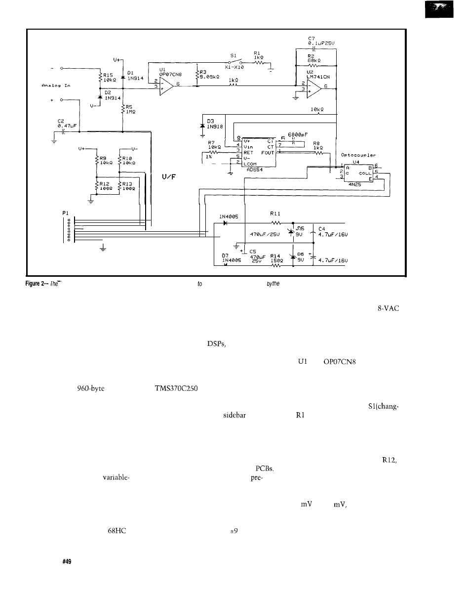
THE NUTS AND BOLTS
Referring to Figure 2, you will see
While many embedded projects
a half-wave-rectified, zener-regulated
use the ubiquitous 803 1 or
11,
power supply providing volts to run
I’ve done numerous successful projects
the circuitry on board. There is no
powers each preamp individually. This
allows each preamp input to be
transformer on this board; instead, a
completely floating, both with respect
to ground and to each other.
small transformer with a dual
secondary mounted on another board
is an
op-amp used
as the input buffer. This high-quality
device has very low input offset
current and is very stable. The gain of
this stage is either 1 or 10 depending
upon the setting of switch
ing would allow for other gain
ratios to be selected if desired). The
input signal is referenced to a variable
bucking voltage that comes from the
wiper of a lo-turn zeroing pot that is
located off-board. The values of
R13, and the pot itself could be
changed to suit a particular application
or eliminated completely. This
particular preamp has a full-scale input
of 10
or 100
depending upon
the setting of S 1.
U2 is an inverting amplifier with a
gain of 68. The preamp is designed to
produce 6.8 V at the output of U2 with
16
Issue
August 1994
The Computer Applications Journal
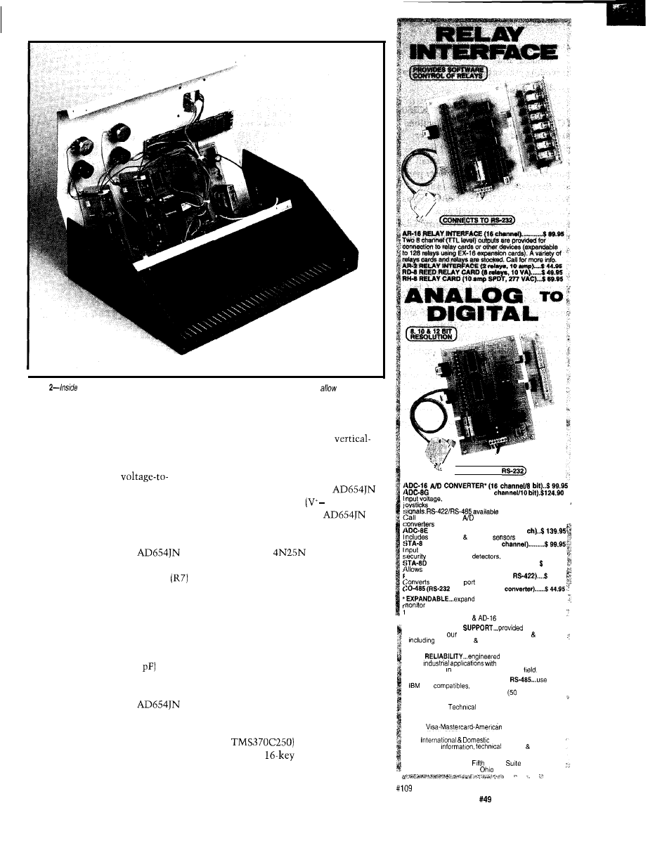
Photo
the printer recorder, the amplifier
modules may
be unplugged and replaced to
the recorder to
be used in many different applications.
the rated input voltage applied. The
count value of 833. The software maps
741 will not produce much more
these counts directly into a
output voltage than this with a 9-V
axis dot position. Since the printer’s
supply, and I make use of this clipping
dot resolution is 960, there is about a
to ensure the AD654
15 % overrange capability. I must note
frequency converter is never driven
that the input signal to the
beyond its full scale (it acts erratically
should never exceed 4 volts). To
when overdriven). A single-pole RC
satisfy this criterion, the
is
filter made up of R2 and C7 filters out
fed from the unregulated power rail
high-frequency noise.
(approximately 12 VDC).
The Analog Devices
VFC is a very simple, yet versatile,
device. The value of the resistor
from pin 3 to ground sets the full-scale
input range (V full scale = 0.001 amp x
R7). In this case, it is 10 V full scale.
The combination of R6 and D3 remove
any negative input signal greater than
one diode drop. The full-scale fre-
quency is set by Cl (6800
to
provide a nominal value of 14700 Hz.
With the rated input signal applied to
the preamp, input to the
is
68% of its full-scale input voltage.
This leads to a full-scale pulse train
frequency of 14700 x 0.68, or 9996 Hz.
A simple
optocoupler with
a transistor output is used to couple
the pulse train to the microcontroller
while maintaining ground isolation.
THE DIGITAL SIDE
As shown in Figure 1, the micro-
controller handles five discrete
functions:
1) electronic switching (4052 CMOS
multiplexer) to rapidly switch
between the pulse trains from the
two channels,
The counting time for each
sample is 83.3 ms, yielding a full-scale
2) pulse accumulation (part of the
to count the pulses,
3) reading a
matrix keypad for
parameter entry,
(
C O N N E C T S T O
A/D CONVERTER* (8
amperage, pressure, energy usage,
and a wide variety of other types of analog
(lengths to 4,000’).
for info on other
configurations and 12 bit
(terminal block and cable sold separately).
TEMPERATURE INTERFACE* (8
term. block 8 temp.
(-40’ to 146’ F).
DIGITAL INTERFACE’ (8
on/off status of relays, switches, HVAC equipment,
devices, smoke
and other devices.
TOUCH TONE INTERFACE* . . . . . . . . . . . . . . . .
134.90
callers to select control functions from any phone.
‘S-4 PORT SELECTOR (4 channels
79.95
an RS-232
into 4 selectable W-422 ports.
to RS-42ZRS-485
your interface to control and
up to 512 relays. up to 576 digital inputs, up to
26 analog inputs or up to 128 temperature inputs using
he PS-4, EX-16, ST-32
expansion cards
FULL TECHNICAL
over the
telephone by
staff. Technical reference disk
test software programming examples in
Basic, C and assembly are provided with each order.
“HIGH
for continuous 24
hour
10 years of proven
performance the energy management
-CONNECTS TO RS-232, RS-422 or
with
and
Mac and most computers. All
standard baud rates and protocols
to 19,200 baud).
Use our 800 number to order FREE INFORMATION
PACKET.
information (614) 464.4470.
‘24 HOUR ORDER LINE (800) 842-7714
Express-COD
FAX (614) 464-9656
Use for
support orders.
ELECTRONIC ENERGY CONTROL, INC.
380 South
Street,
604
Columbus,
432155438
The Computer Applications Journal
Issue
August
1994
17
4) sending data to a 2 x 40 LCD
module, and
5) sending printer data to a Centronics
parallel port.
My general-purpose
PC
board contains all of the functions
just described except for the printer
port (which I didn’t need in other
projects). Therefore, I wired a small
protoboard to contain the printer port
and the preamp power transformer.
While the
PCB contains
its own 5-V supply as well as an
isolated supply for other circuitry, I did
not have two isolated 8-V transformer
secondaries to spare.
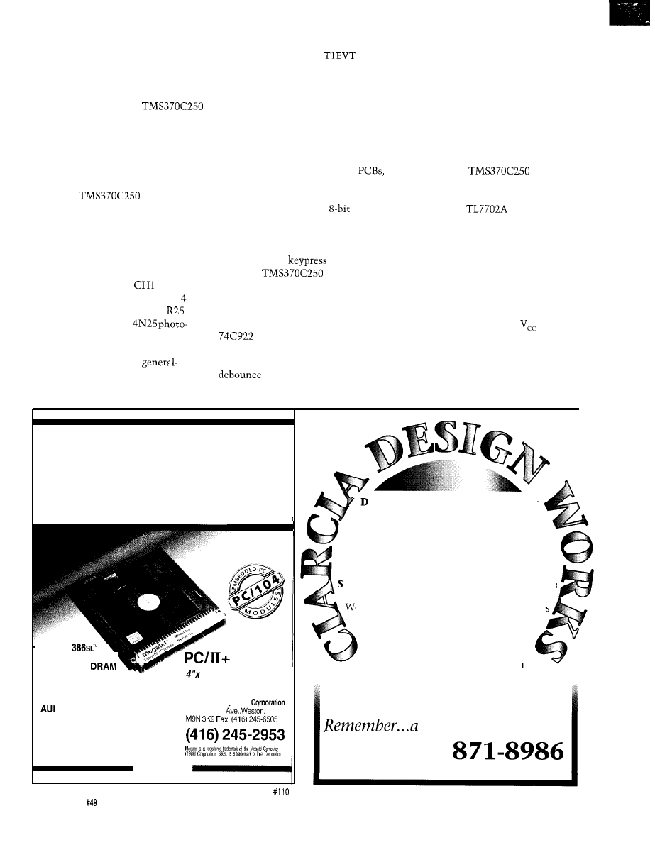
Referring to Figure 3, the optically
isolated pulse trains from the two
preamp/VFCs, labeled
and CH2,
are fed to U8, a CMOS 4052 dual
channel multiplexer. R23 and
are
collector loads for the
transistors. I don’t use the TMS370
Interrupt 3 pin as an interrupt input,
but instead set it up as a
purpose output to act as address line A
of the 4052 mux to do the channel
switching. The pulse train enters the
microcontroller via the
pin.
This pin can be used to clock either
the Timer 1 module or the watchdog
counter. In most cases, including on
this project, I use the watchdog
counter to accumulate pulses and
leave the other two multifunction
counter/timer modules free. Trans-
former T2 has dual 8-V secondaries to
power up the two preamp/VFC
as I described earlier.
While it is possible to scan a small
keypad directly using an
port and
software, many of my projects require
the microcontroller to do accurate
time-related functions, but also be
responsive to a
at any time.
Since the
has no
internal EPROM or ROM, it must
supply a complete data/address bus,
resulting in very few general-purpose
I/O pins left over. Therefore, I used a
keypad scanner chip, which
directly connects to the data bus as a
peripheral and contains all the key
circuits and a Data Available
pin.
Two
5-V power supplies are
shown in Figure 4, one of which runs
the entire microcontroller board. The
other supply was present on the PCB
for other purposes, but I use it in this
case to power the Centronics parallel
port, though that could also have been
connected to the main 5-V supply.
Figure 3 also shows the actual
microcontroller and associated support
circuitry. The
runs at 20
MHz, which it divides internally by 4,
giving a cycle time of 200 ns. Note the
existence of a
power supervi-
sor IC controlling the -RESET line.
Since some of the projects using this
board control critical devices such as
large heaters or high-voltage power
sources, I felt it critical to add a
supervisor IC like this to shut down
the controller if the power supply
drops or to reset it if a power surge
momentarily disrupts the
supply.
Also, the integrity of the on-board
EEPROM contents is assured by this
supervisor since the processor will not
execute code wildly every time it is
powered down. For this particular
Embedded
P C
with on-board
Ethernet
and
Super VGA
l
25 MHz
CPU; including up’
to 10 MByte
l
On-board Super VGA
LCD/Video controller
l
On-board Ethernet, Featuring
4” Small
Rugged format
For more information call:
Meaatel Comouter
and 10 BASE-T interfaces
125Wendell
Ont.
l
On-board SCSI, Floppy controllers and
2 MByte Flash Eprom Solid State Disk
l
3 Serial Ports,
Parallel/Printer port
megatel
oes your Big-Company marketing
department come up with more ideas
than the engineering department can
cope with? Are you a small company
that can’t afford a full-time engineering
staff for once-in-a-while designs?
teve Ciarcia and the Ciarcia Design Works
staff may have the solution.
e have a team of accomplished programmer
and engineers ready to design products
or solve tricky engineering problems.
Whether you need an on-line solution
for a unique problem, a product for a
startup venture, or just experienced
consulting, the Ciarcia Design Works
is ready to
work with you.
Just fax me your problem and we’ll be in touch.
Ciarcia design works!
Fax (203)
18
Issue
August 1994
The Computer Applications Journal
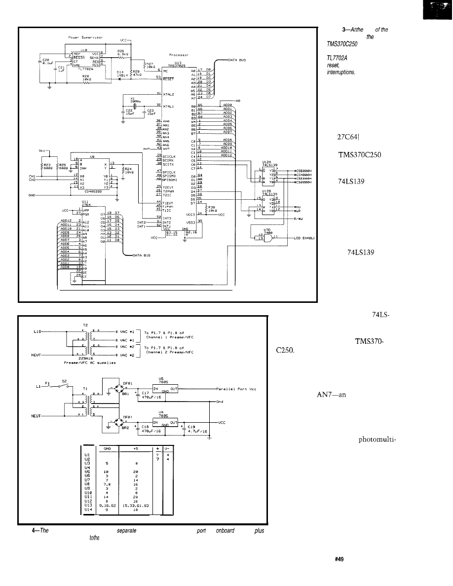
Figure
power supply section develops
5-V supplies for fhe parallel
and
circuitry,
if
provides unregulated
AC power
preamp boards.
Figure
core
printer recorder is
processor and 8
KB of program
memory.
A
ensures a reliable
even after brief power
application, a simple
RC reset circuit would
suffice.
The single 2764
(or
EPROM
interfaces directly to
the
controller. The *OE
signal is derived from
the
device
decoder, which also
acts as the device
selector for all other
peripherals. Rounding
out this figure is an
active-low device
select signal provided
by the
decoder. The signal is
inverted by a single
section of a 7400
NAND gate.
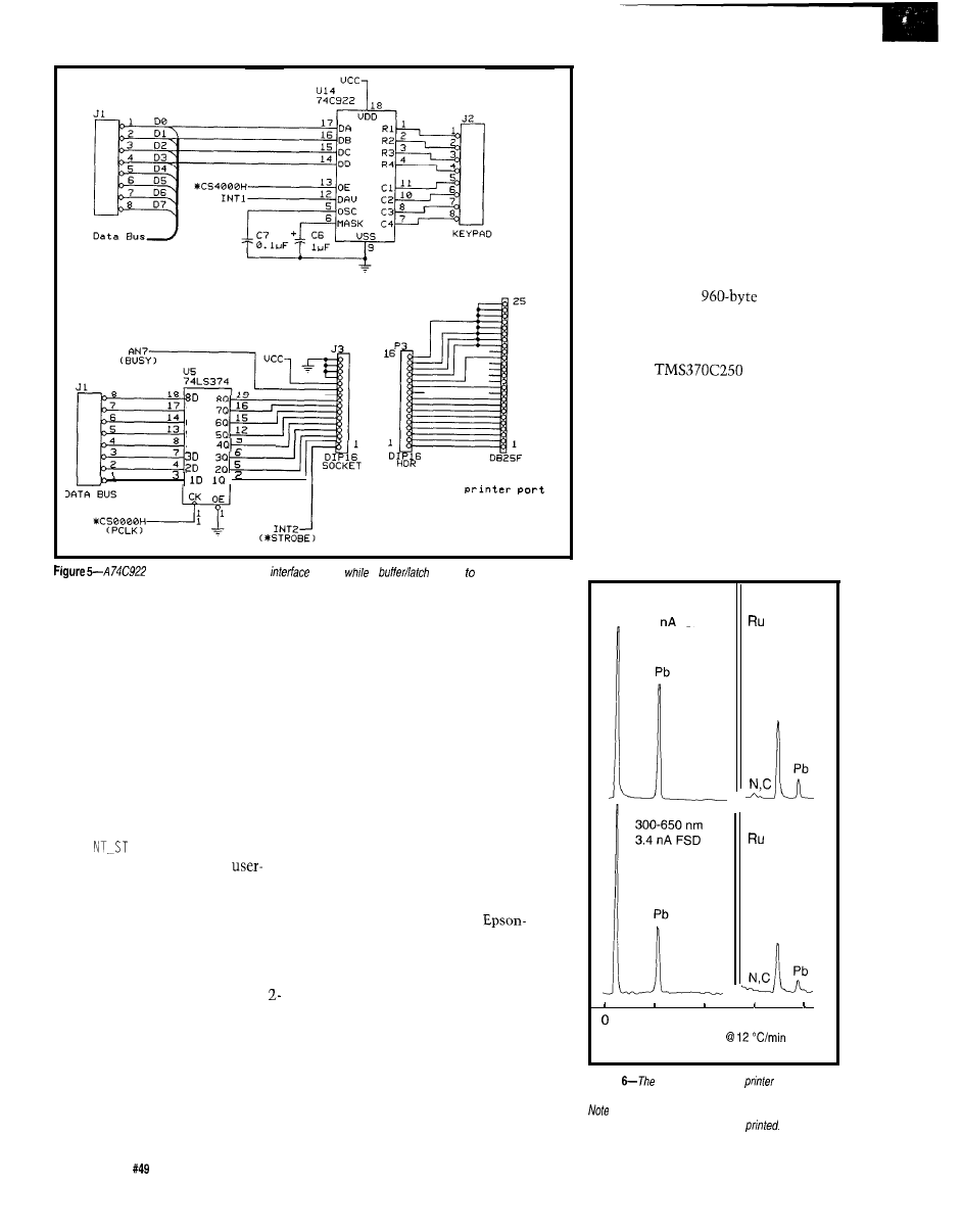
Figure 5 shows
the printer port
circuit. I use a
374 octal latch as the printer data
latch. The printer -Strobe signal is
generated by INT2 of the
INT2 is another external
interrupt input on the micro that I’m
using instead as an output bit. The
only status signal from the printer that
is read is the Busy signal, which is
connected to
analog input
set in software to a digital input.
Figure 1 is an interconnect
diagram for the whole project. The
photos depict a unit designed to
measure current from two
plier tubes. As such, the preamps differ
from the ones described. The photos
also show a new PCB which replaces
the general purpose TMS370 PCB and
printer port/power supply board that
were used when the article was
submitted.
THE FIRMWARE
The firmware that operates the
printer/recorder uses less than 4K of
The Computer Applications Journal
Issue
August 1994
1 9
The TMS370 Microcontroller Family
The
TMS370 family of microcontrollers from
a separate latch to demultiplex the address bus,
Texas Instruments is a diverse one. The
ing the PC board design.
devices are low-end controllers in
DIP and PLCC
The maximum clock speed is 5 MHz using an
packages targeted at large-volume applications using
external
crystal. Most instructions execute in
mask-programmed ROM. The ‘x30 and ‘x40 devices
10 cycles, with the
divide instruction taking the
contain more functionality and come in larger DIP and
longest at 63 cycles.
PLCC packages. The top of the line is the ‘x50 group of
The instruction set is much like the Intel 803 1
controllers, which is what I have chosen to use in my
family in that it has a rich mix of instructions,
designs. While there are devices in this group containing
ing modes, and bit operations, but lacks the 16-bit
either mask ROM or OTP EPROM for program storage, I
operations of the Motorola
and 68HC 11 devices.
chose the inexpensive
The only pseudo-16-bit operations supported are 16-bit
version
PLCC). This is the most cost-effective
MO V W instructions and the I N C X instruction, which can
approach since
EPROMs are very inexpensive.
add a signed
constant to a 16-bit register.
When the
is configured for
The assembly language conventions are a bit hard to
external program memory, it yields a microcontroller
get used to for anyone who has used both Intel and
with the following features:
Motorola parts. While the MOV opcodes use Intel conven-
tion, the source-destination ordering of the operands is
1) 256 bytes RAM,
Motorola convention.
2) 256 bytes EEPROM (block protectable),
Texas Instruments sells a TMS370 application board
3) channels of fast
A/D conversion,
that works in conjunction with a host PC computer via
4) two very flexible counter/timer modules with features
an RS-232 link. The board itself contains two ‘x50
such as programmable prescaling, PWM function
devices: a master unit, which communicates with the
generation, and pulse accumulation,
host PC, and a slave unit.
5) watchdog timer (associated with one of the above
The slave shares memory space with the master
timers, but more or less independent),
(which loads it) and runs the user’s application in real
6) a full-duplex Serial Communication Interface with
time, with access to the peripheral ports and other I/O
programmable baud rate (independent of the timers
devices. The
group of devices is also supported on
above),
this board. The host PC runs a windowed monitor/
7) a bidirectional three-wire Serial Peripheral Interface
debugger/tracer program which is supplied with the
with programmable transfer speed,
application board. Cross-assembler software to run on
8) three external interrupt inputs which can be either
the host PC is also provided, and a C cross-compiler and
level or edge sensitive and are polarity
linker are available separately.
mable, and
Texas Instruments runs a BBS devoted to this
9) pins associated with functions 3-8 above that are not
product family and it contains free software and
needed for their original purposes may be reassigned
tion. Of particular use to new users is the
monitor
as general-purpose I/O lines (some are input only).
program which fits in a
EPROM. Adding a
and a MAX232 produces a fully functional
The
device provides 16 memory
stand-alone evaluator. Floating point and other useful
address lines and 8 data lines, so there is no need to use
core routines are also available.
memory, residing in the upper half of a
invoked by the Timer 1 interrupt (10
which has been accumulating the V/F
EPROM. I will first briefly
Hz). Timer 1 not only interrupts at a
counts, then resets this counter.
describe the overall program before
rate, but also generates a PWM
2) converts this count to a
going into detail about the P R I NT_
gating signal for the V/F pulse
ing-point number.
ST R I P routine which is the core.
lation. The V/F pulses are counted for
3) toggles a variable and the INT3
Upon reset, the program prompts
for the current date and then goes into
the parameter mode loop which allows
the operator to select a chart speed and
a filter time constant. Once those are
entered, the program goes into the first
phase of the acquisition mode loop.
All data acquisition is performed
by an interrupt service routine (ISR)
83.3 ms out of the
interrupt
period. I chose 83.3 ms because it
equals five line cycles, thereby giving
some line-noise reduction due to
integration.
The Timer 1 ISR performs the
following functions in sequence:
1)
reads the watchdog counter,
pin, which drives an address line of the
4052 analog multiplexer IC, thereby
alternately reading both of the preamp
input channels.
4) adds the current count (in
floating point) to an accumulator and
multiplies the result by a constant
selected by the user’s choice of filter
time constant. This result is then
The Computer Applications Journal
August1994
21
7 D
6 D
SD
4 D
1 6
I
R e a r P a n e l M o u n t e d
C e n t r o n i c s
encoder keeps the keypad
ample,
a
is used interface to the
printer.
restored to the accumulator (this is a
moving weighted-average algorithm
that acts like a one-pole RC filter).
5) decrements the counter variable
SAMCT
and when it equals zero, the
floating-point accumulator value is
scaled and converted back into an
integer in the range of O-959 (the
number of dots of printer resolution
across the page). This value is saved as
one of eight points which will later
make up a strip to be printed using the
P R I
R I P
routine. The value of
SAMCT
is determined by the
selected chart speed.
6) calls the routine N
E E D L E
for
each printer data point stored above to
place a thin line on the LCD. The line
acts as a pseudoanalog meter for the
user’s convenience in setting up the
gain and zero of the recorder. The
line LCD allows one line per channel. I
use the first 32 characters of each line
for the analog “needle” and the last
eight for display of the elapsed run
time. The 32 characters allocated for
the “needle” are further broken down
into four positions per character,
giving a resolution of 128, which is
quite adequate for the purpose.
7) updates the Elapsed Time
Clock.
All of these functions take place
in an interrupt-driven fashion while
the user “fusses” with the gain, zero,
and the device being measured. When
satisfied that all is well, the operator
hits any key on the keypad and the
real fun begins. In addition to the
Timer 1 ISR functions listed above,
after eight data points [per channel) are
collected into an array, the
P R I NT_
STR I P
routine is called. This routine
prints out the data to the
compatible printer through the
Centronics parallel port on the
microcontroller board.
After printing these eight points,
the pointers to the two arrays are set
back to the beginning and the process
repeats until the user hits a key on the
keypad to end the run. At that time,
the microcontroller sends to the
printer ASCII strings representing the
date, elapsed time, chart speed, a
device name, and a sequential run
serial number. The little report at the
end of each run is often very useful in
keeping data straight for those who do
not keep good lab notes of their own!
THE PRINT-STRIP ROUTINE
This routine takes the eight data
points for each channel and prints the
equivalent of the two pen traces on
the paper. This requires a transform of
the eight amplitudes of two channels
into the printer’s
graphic
bitmap array. That is to say, we must
supply the printer with 960 bytes of
graphics data per strip of data printed.
Since the
contains only
256 bytes of RAM for all program
variables, the program must do this
data transform on the fly. Of course,
the micro is also collecting and
filtering data and updating a real-time
clock at the same time, so the
TMS3 70 is kept very busy indeed.
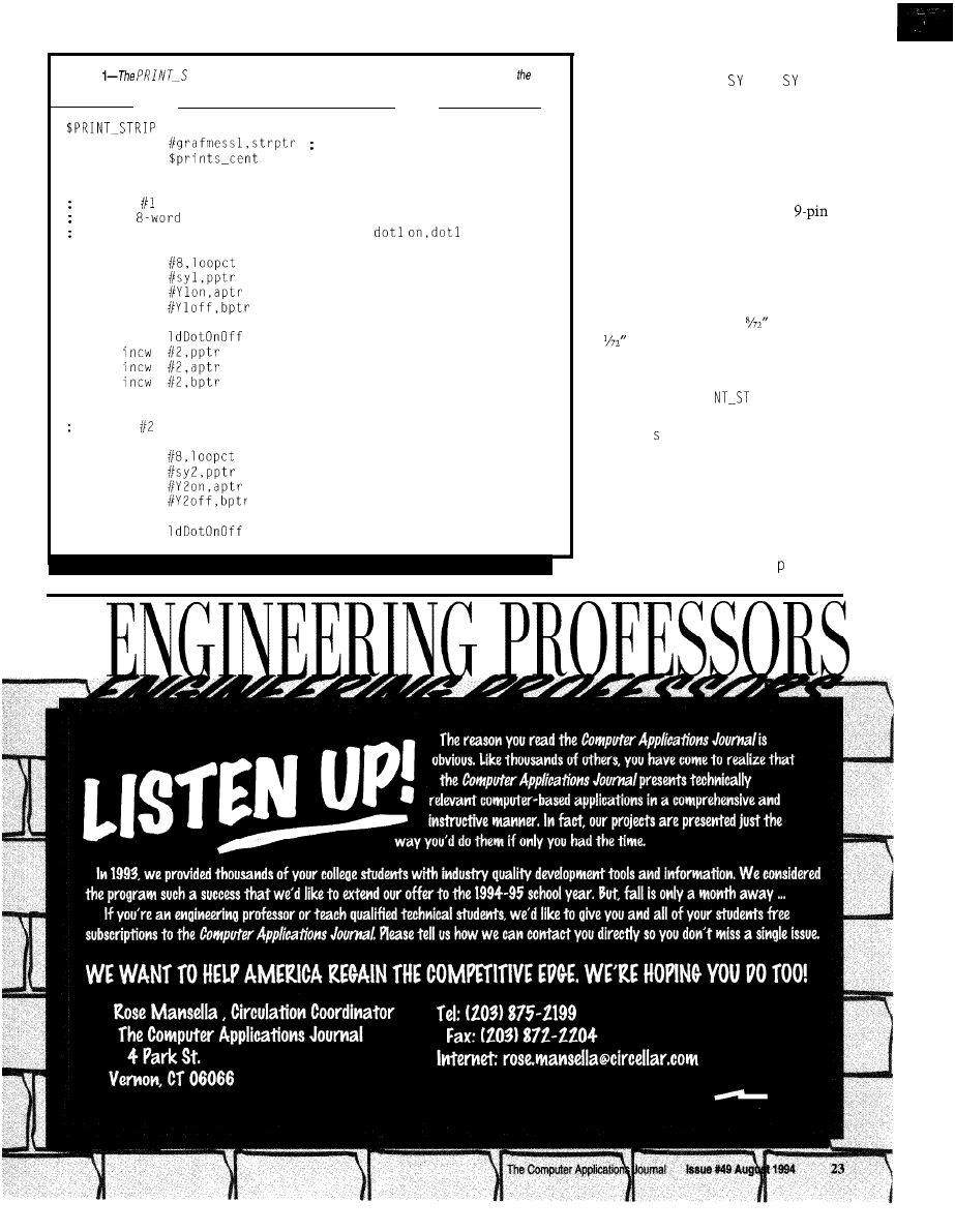
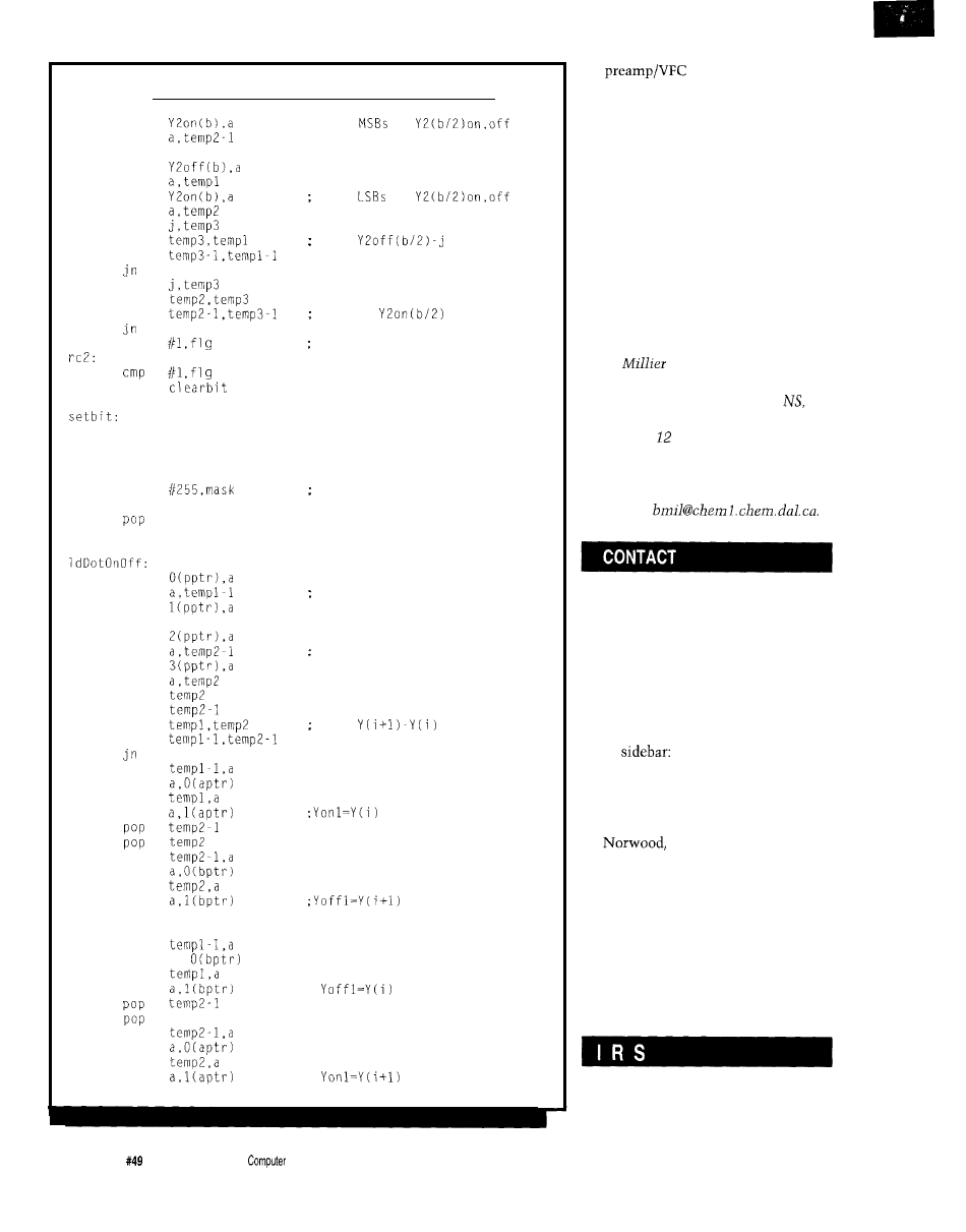
Listing 1 contains the assembly
code for this subroutine. Prior to
calling this routine, nine data points
300-650
nm
3.4
FSD
Pb
300-650 nm
3.4
FSD
Pb
C r
Pb
C r
4
min
8
1 0 0
1 5 0
2 0 0
Figure
actual output of the
recorder is
every bit as useful as that from a real strip recorder.
that the labels were added after the printout was
complete and are not automatically
22
Issue
August 1994
The Computer Applications Journal
Listing
TR I P routine must convert the linear data into the dot array required by
printer.
movw
pnt to Epson graphics cmd str
call
clr
pbyte
CHANNEL
make an
array of dot on/dot off values: 1 for each pixel
point to start of three arrays: datal,
off
mov
movw
movw
movw
ldloopl:
call
djnz
loopct, ldloopl
CHANNEL
mov
movw
movw
movw
ldloop2
call
(continued)
from each of the two channels have
been stored in arrays 1 and 2.
These are unsigned 16-bit integer
values, prescaled to the range O-959.
Nine values are needed since we must
know the “position of the pen,” so to
speak, from the last strip printed. This
adds one extra data point to the eight
we wish to print. Although the
printer has the ability to print nine
dots per pass, only eight of them are
used to keep all operations in byte-size
chunks. The main program has already
sent the printer a command sequence
to set its line spacing to
(each dot
is
and eight dots are printed per
pass]. This is done only once at the
start of a run.
The actual
P R I
R I P
routine
starts by sending the string at the label
g r a
f me s 1 to
the printer. This is the
Epson command for Graphics Mode 2
(960 dots resolution). This command
must
be repeated for each printing
pass.
The code starting at label
1 d
Loop 1
examines the eight pairs of
data points from channel 1 (d 1 and
Listing l-continued
SOLID STATE DISK
Card 2 Disk Emulator
EPROM, FLASH and/or SRAM
Program/Erase FLASH On-Board
Total,
Drive Bootable
25MHZ 386DX CPU $695”
Compact AT/Bus or Stand Alone
In-Board
IDE, FDC, 2
FLASH&RAM Drives to
Cache to
DRAM to 48M
TURBO XT
w/FLASH DISK
To 2 FLASH Drives,
Total
DRAM to 2 M
FLASH On-Board
CMOS Surface Mount, 4.2” 6.7”
2
Par, Watchdog Timer
Tempustech VMAX products are
PC B
US
Compatible. Made in the
J.S.A., 30 Day Money Back Guarantee
1,
breaks start at 5 pieces.
TEMPUSTECH, INC.
643-4981
for
295 Airport Road
ast response!
Naples, FL 33942
djnz
loopct,
mov
call
clr
djnz
mov
mov
$9
movw
clr
mov
mov
bitlp:
call
inc
clrc
rrc
djnz
mov
jne
cmp
jhs
or
$8
call
cmp
jne
cmp
jne
b
b
mask
$8
$8
Sprint-cent
movw
call
rts
clr
mov
mov
mov
mov
inc
mov
mov
mov
mov
movw
sub
sbb
b
a,templ
movw
sub
sbb
jn
rcl
rcl:
dec
mov
mov
rcl
b
print axis
; 9
passes of
inch = 1 inch
axis tick at center of strip
l-959 (pixels across page)
locations for dot
advance ptr to next data point
; add in time blip
output the byte to printer
advance to next Y pixel
; all 960 strips sent to printer
send CR-LF to printer
RANGE COMPARE CHANNEL
load
of
load
of
form
form
set the flg for a dot on event
RANGE COMPARE
2
2 4
Issue
August 1994
The Computer Applications Journal
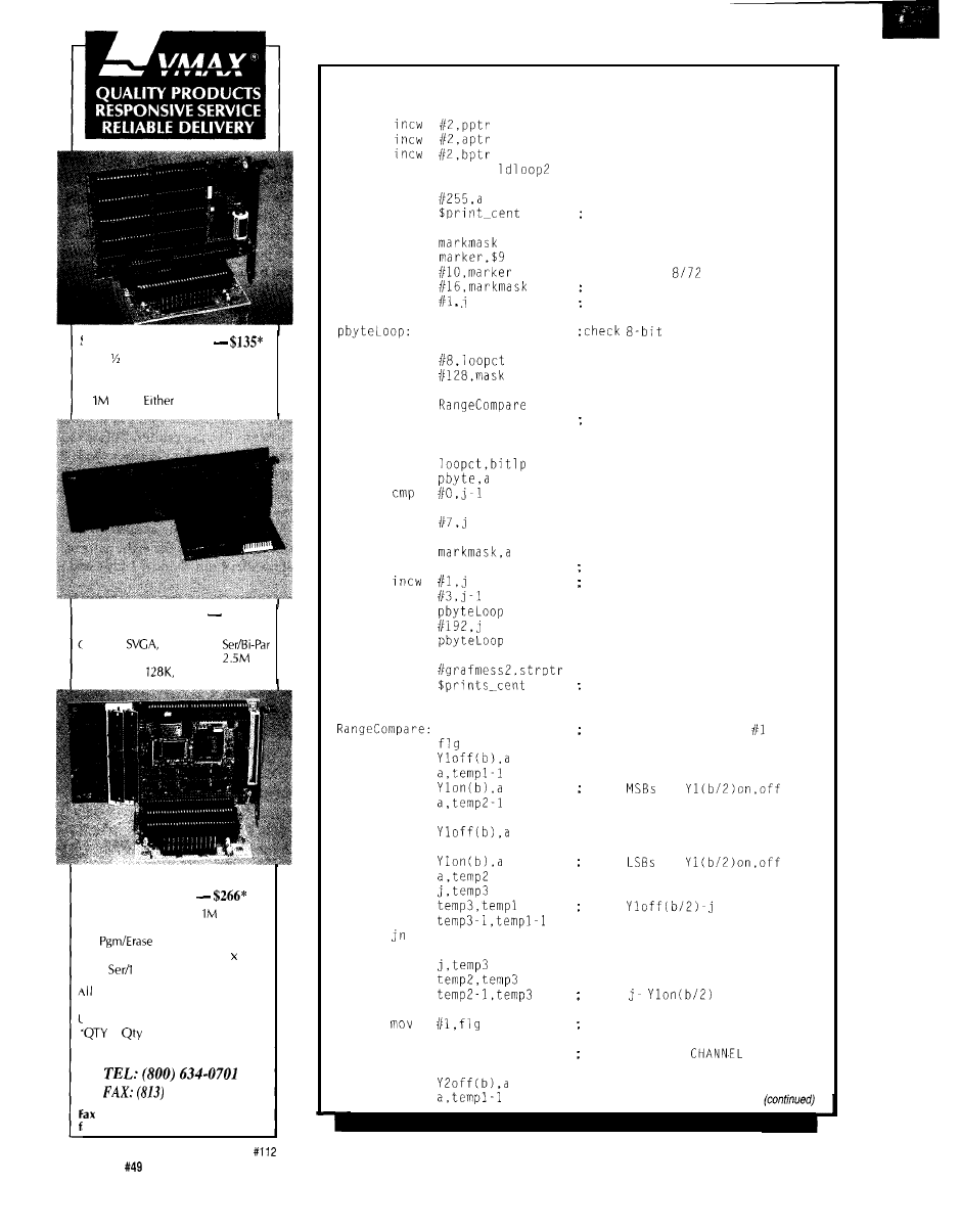
dp2, dp2 and dp3, etc.) and determines
where the dot for that data point
should start printing and where it
should stop printing. It produces an
array of eight “dot
words and eight
“dot off” words, designated Y
and
Y 10 F F, respectively. The code starting
at 1 d Loo performs the same for
channel 2.
Once I know the range in which a
dot must be printed for each of the
eight dot positions per pass, I then set
up a loop to send out 960 bytes to the
printer. That loop starts at label
p by e Loop in the listing.
The print head in the Epson
printers is set up so its upper pin is
designated by the most-significant bit
of the graphics data byte sent to it (i.e.,
128 decimal). The way the printer is
used for this application, this upper-
most pin corresponds to the first data
point taken in the group of eight that
are to be printed per strip. The p by t e
Loop initially sets up the variable
MASK equal to 128 and calls subroutine
to see if either channel
needs that dot turned on or off.
Depending on the outcome of that
check, it either sets or clears the bit in
the position specified by the mask.
This is repeated eight times: each time
the mask value is changed to corre-
spond to the next dot position (by a
“rotate right” of MASK).
After these eight iterations of the
loop, the variable p by e is almost
ready to be sent to the printer. Before
sending it to the printer, however,
some checks are made to see if
anything must be added to the data. As
a convenience to the user, a baseline
axis is printed and a small tick is
added to this baseline for every inch of
paper travel. Examine the code
following the label b i 1 p for details of
this operation.
After 960 iterations of the
p by e Loop routine, a carriage return
and a
are’sent to the printer.
At this point, the P RI
R I P
routine returns to the main program.
“OUT OF PAPER”
That’s the overall description of
the printer recorder. We are using a
number of these instruments success-
fully in our research labs. By placing
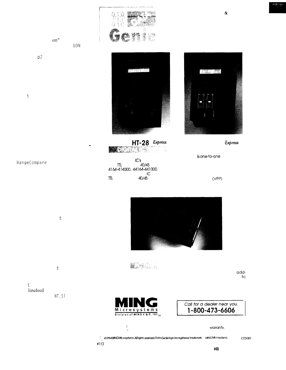
Data Genie
offers a full line of test measure-
ment equipment that’s innovative, reliable and
very affordable. The ‘Express Series” of stand-
alone, non-PC based testers are the ultimate
in portability when running from either battery
or AC power.
Data Genie products will be
setting the standards for quality on the bench
or in the field for years to come.
The HT-28 is a very convenient way
of testing Logic
and DRAM’s Tests
most 74, CMOS
and DRAM’s
It can
also identify unknown numbers on
74 and CMOS
series with the
‘Auto-Search’ feature.
$189.95
HT- 14
The HT-14
EPROM writer
with a super fast programming speed
that supports devices from 27320 to
27080, with eight selectable pro-
gramming algorithms and six pro-
gramming power
selections.
$289.95
P-300
The Data Genie P-300 is a useful device that allows you to quickly install
on cards or to test prototype circuits for your PC externally. Without having
turn off your computer to install an add-on cards, the P-300 maintains com-
plete protection for your motherboard via the built-in current limit fuses
$349.95
17921 Rowland Street
City of
Industry. CA 91748
TEL (818) 912-7756
FAX (818) 912-9598
Data Genie products are backed by a full
lyear limited factory
of
The Computer Applications Journal
Issue
August 1994
25
Listing
l-continued
mov
mov
inc
mov
mov
mov
mov
movw
sub
sbb
movw
sub
sbb
mov
jne
or
rts
clearbit:
push
xor
and
rts
mov
mov
mov
mov
mov
mov
mov
mov
push
push
sub
sbb
mov
mov
mov
mov
mov
mov
mov
mov
rts
$1
mov
mov
mov
mov
mov
mov
mov
mov
rts
load
of
load
of
form
rc2
form j-
rc2
set the flg for a dot on event
mask,pbyte
mask
mask,pbyte
mask
invert mask
get first of two dpoints
a,templ
and second
form
$1
a,
temp2
the
on a separate PCB,
I’ve been able to design several
different preamp modules for different
applications. Figure 6 shows an actual
printout from the device connected to
a chromatography apparatus. Special
thanks is extended to Dr. Walter Aue,
whose large research group never
seems to have enough instrumenta-
tion. It was this need which spawned
the idea in the first place. Possibly
some of the concepts outlined here
could also find some use in low-cost
hard-copy data logging in industrial
process control.
q
Brian
has worked as an
instrumentation engineer at
Dalhousie University, Halifax,
Canada in the Chemistry Department
for the past years. In his leisure
time, he operates Computer Interface
Consultants and has a full electronic
studio in his basement. He may be
reached at
Texas Instruments, Inc.
9301 Southwest Fwy.
Commerce Park, Ste. 360
Houston, TX 77074
(713) 7786592
TI Microcontroller Technical
Hotline: (713) 274-2370
BBS mentioned in the TMS370
(713) 274-3700
Analog Devices
One Technology Way
P.O. Box 9106
MA 02062-9106
(617) 329-4700
Fax: (617) 326-8703
LCD Display
Timeline, Inc.
23605 Telo Ave.
Torrance, CA 90505
(310) 784-5488
Fax: (3 10) 784-7590
401 Very Useful
402 Moderately Useful
403 Not Useful
26
Issue
August 1994
The
Applications
Journal
J. Conrad Hubert
Get Precise, with the
A/D Converter
Collect Lots of Precise Data with
this
ADC
0
raditionally,
high-resolution
have relied on
the techniques of
successive approximation and
slope integration to achieve accuracy
greater than
15
bits. Although these
techniques have served well in the
past, they are not without drawbacks.
Precision successive-approximation
converters require complicated
trimming and/or calibration schemes
and are expensive. Similarly,
slope converters require accurate
comparators and expensive
and-hold circuits. They are also
extremely slow.
During the last five years,
based on what is called
sigma-delta
modulation
have become commer-
cially available. Although sigma-delta
modulation techniques have been
around since the early
they
were not often implemented because
they impose a substantial digital signal
processing burden.
Converters based on the sigma-
delta architecture do not require
precisely matched components.
Instead, they use a 1 -bit quantizer
(comparator) in a feedback loop. High
resolution is achieved by oversampling
(which shifts noise to higher,
band frequencies) and on-chip digital
filtering.
Unlike conventional
sigma-delta converters don’t require
sophisticated antialiasing filters or
sample-and-hold amplifiers. This is
because their input sample rate is
higher than the rate for other tech-
niques which provide the same
bandwidth.
What’s more, the sigma-delta
technique lends itself to implementa-
tion in a digital CMOS process,
Usually, a silicon process is optimized
for either analog or digital circuitry. It
is difficult to add high-performance
analog circuitry to primarily digital
real estate. DSP chip makers are
excited about sigma-delta because it
will allow them to embed the ADC
right on the DSP chip itself. In fact,
because sigma-delta
are reason-
ably tolerant of switching noise, the
architecture is uniquely suited to life
inside digital computers.
Now that I’ve extolled the virtues
of the sigma-delta architecture, I will
remind you that there is, of course, no
free lunch. Remember the “l-bit
quantizer in a feedback loop”? Well, it
points to perhaps the only disadvan-
tage of the sigma-delta architecture:
poor DC stability. (Other more
complicated implementations of the
sigma-delta architecture can provide
excellent DC stability at the expense
of lower conversion rates. Crystal
Semiconductor makes such parts, but
refers to them as delta-sigma A/D
converters.) One other potential
disadvantage is that multichannel
systems usually require a separate
sigma-delta converter for each chan-
nel. Multiplexing is possible, however,
provided sufficient time is allowed for
the digital filter to “settle” prior to
accessing data from the next channel.
The bottom line is that sigma-
delta converters are best suited to
applications which require high
sampling rates along with an ex-
tremely good signal-to-noise ratio and
excellent differential linearity. Typical
applications include signal processing,
digital audio, communications, and
ISDN (Integrated Services Digital
Network).
28
Issue
August 1994
The Computer Applications Journal
One example of a sigma-delta
converter implemented in silicon is
the Motorola
This
low-cost ($24 in 100s) ADC provides
resolution at up to 100,000
samples per second (Sps) while
consuming less than 0.5 W from a
single 5-V supply. Recently, Analog
Devices began second-sourcing this
part as the AD776.
In the remainder of this article, I’ll
describe how to build a simple
based data acquisition board around
the
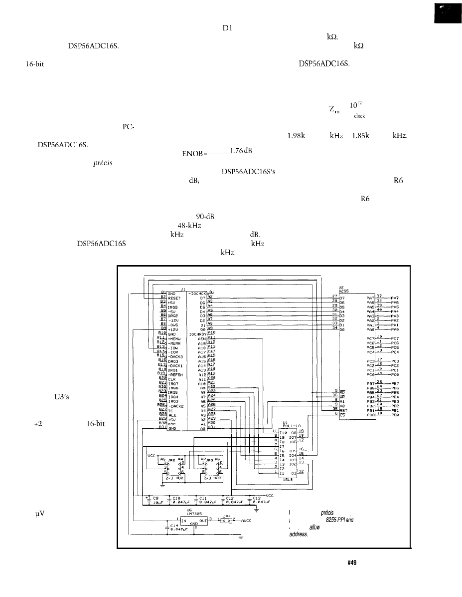
The schematic for
the design appears in Figure 1. The
board was christened
after the
French word for “exact”. I’ll describe
the precis hardware in six sections,
starting with the ADC and working
my way to the bus interface. The
printed circuit board and software will
be covered last.
to-back zener diodes
and D2. If the
absolute value of the voltage into the
BNC is greater than the zener voltage
plus a forward diode drop (3.8 V), these
diodes short-circuit the source driving
precis and clip the input signal.
One measure of the “goodness” of
an ADC is its ENOB, or effective
number of bits. ENOB is to an ADC’s
accuracy what word length is to an
ADC’s precision. The ENOB for any
analog-to-digital converter is related to
its SNR specification by the equation
SNR-
6.02
Motorola quotes the
SNR at 90
however, that figure
represents best case conditions. A
more realistic figure appears in the
Analog Devices data sheet, which
states that a
SNR is achieved
with a
sampling rate, and at
100
the SNR drops to 86
This
yields an ENOB of 14.66 at 48
and
just under 14 at 100
The input impedance of precis is
nominally 2
However, the actual
input impedance is 2
in parallel
with the dynamic input impedance of
the
The converter’s
impedance is a function of its clock
frequency, and is related by the
equation
= 3F
The input impedance ranges from
at 12.5
to
at 100
Because the ADC’s input imped-
ance is a function of clock frequency,
the loading on the input bias circuit
changes somewhat with clock fre-
quency. Therefore, potentiometer
is provided to null the input offset.
With the BNC shorted,
should be
adjusted in real time to yield an offset
of zero for a given acquisition rate.
(The actual offset may fluctuate
slightly.)
You may infer (correctly) from the
preceding paragraph that the input
ADC
Because the
(U3)
samples its analog input 64 times
more often than it
produces a digital output,
a high-order antialiasing
filter is not required.
Motorola does, however,
recommend installing a
simple single-pole filter
prior to the ADC. This
filter should be made
from a high-quality
polystyrene capacitor
(C5) and two metal film
resistors (R2 and R3).
An input range of 4 V
peak-to-peak is realized
by using
on-chip
voltage reference (nomi-
nally 2 V). Thus, an input
of V results in a
two’s complement output
word equal to 32,767. A
-2-V input produces an
output code of -32,768.
Shorting the input
connector yields an
output code of 0. From
these values, one can
calculate a sensitivity of
61
per LSB.
Bipolar overvoltage
protection for the ADC is
accomplished via back
Figure la--The
bus interface consists
primarily of an
some
decoding logic.
Jumpers
the user to select a base port
The Computer Applications Journal
Issue
August 1994
29
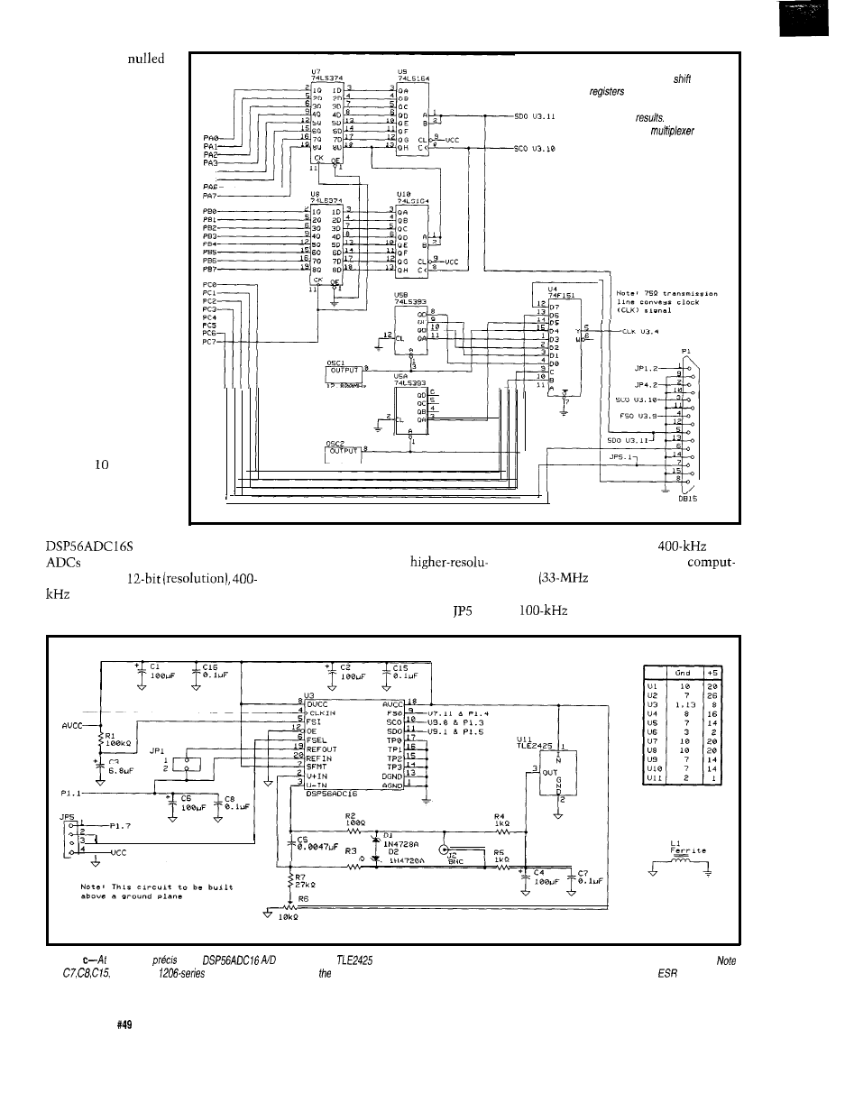
offset must be
separately for every
acquisition rate. If
Figure lb-,4 pair of
and a pat of latches
this is inconvenient,
remember that it’s
possible to cancel the
input offset by adding
a constant to the data
PA4
PA5
once it has been
stored in main
memory. The con-
stant is determined
[for a given acquisi-
tion rate) by shorting
the analog input
terminals and
observing the result-
ing output code. The
difference between
the observed output
code and zero must be
added to each data
point to cancel the
input offset. A typical
value might be
between and 30,
and may well be
negative.
Another interest-
ing feature of the
is that it is really two
fast, low-resolution comb filter and a
make up a double buffer to hold
conversion
Two
counters and a
allow
selection of the acquisition rate.
to provide access to this
data
in one. At the flip of a switch, it
FIR filter with slower,
rate. Unfortunately, even fast
can become a
tion). By holding pin 6 (marked FSEL)
ers
‘486) cannot keep up with
ADC. This is possible because the
high, the digital output is taken prior
that data rate. In practice, only the
part uses two internal digital filters (a
to the FIR filter. The intent of
was
data rate is usable. Therefore,
CLK
I
1 0 0
N U L L
Figure 1
the
core of
is the
converter. The
virtual ground generator produces a voltage precise/y halfway between 5 V and ground.
that
and Cl6 are
SMT capacitors mounted on solder side of the PC board. They may or may not be required depending on the
of the
electrolytic capacitors used.
30
issue
August 1994
The Computer Applications Journal
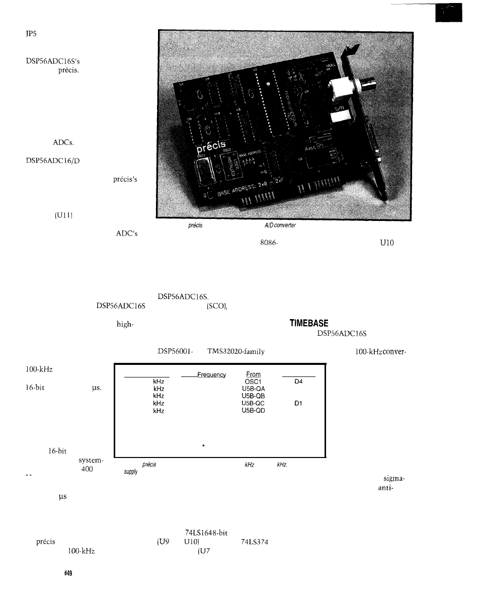
should be configured to tie pin 6 of
u3 low.
That about covers the
analog side as it
applies to
However, let’s cover
two of the part’s idiosyncrasies. Pins
14-17
of the ADC are manufacturing
test points and must be held low
during normal operation. Also, please
observe that the converter is always
running, and that there is no “start”
command as is typical with other
types of
For more information
about the ADC itself, order document
directly from
Motorola.
Finally, the other IC in
front end is due a few words of
explanation. Called a virtual ground
generator
by Texas Instruments, the
TLE2425
produces a voltage
precisely halfway between 5 V and
ground. It is used to bias the
differential input amplifier at one-half
V,,. [A similar part, the TLE2426 is
called a rail
splitter.
This part is
slightly more general purpose, having
an input range of 4-40 V.)
Photo
l-The
high-speed, high-resolution
works in any ISA-bus computer.
SERIAL-TO-PARALLEL
The output of the
is serial rather than parallel because it
is intended to mate with the
speed serial port on Motorola’s 56001
DSP engine. Unfortunately, the serial
data rate is far too high for a PC to
accept directly. At the
sample rate, the
ADC emanates a new
word every 10
However, valid data is
available only during the
second half of that
period. This means the
time available to read
the output word is only
5 us. A
word read
in 5 us implies a
Before detailing the hardware
implementation of the double buffer,
I’ll first describe the digital side of the
It has three outputs:
serial clock out
serial data out
(SDO), and frame sync out (FSO). The
format of FSO is determined by the
serial format (SFMT) input. If SFMT is
pulled low, FSO is compatible with
and
data MSB first while U9 and
are
clocked in parallel until all 16 bits
have been shifted into place. Each time
FSO goes high, a valid word at the shift
register’s output gets clocked into the
latches. Additionally, the FSO signal is
polled by the software to determine
when to read these latches.
The
must be
clocked at 128 times its data output
rate (12.8 MHz for a
Conversion Rate
100
50
25
12.5
6.25
Clock
12.8 MHz
6.4 MHz
3.2 MHz
1.6 MHz
0.8 MHz
User rate
User rate/2
128
l
rate
64 * rate
o s c 2
D6
USA-QA
D5
External
28 rate
External
bus bandwidth of
kbps. However, by
resorting to a double buffering scheme,
the full 10 is available to read the
word and the data transfer rate is
decreased to 200k bytes per second.
Although double-buffering eases the
bus bandwidth requirements enough
for
to run on an AT-class
machine, the
sample rate is
sion rate). Clocking the
M
UX
channel
ADC slower results in
the conversion rates
D3
shown in Table 1.
D2
You may ask, “Why
DO
not just clock the ADC
at its maximum rate,
then store every nth
conversion to achieve a
D7
lower conversion rate.”
Not a bad idea, but it
does have one draw-
back. Part of the
elegance of the
delta architecture is that no
aliasing filter is needed because the
signal is processed by an internal
brick-wall FIR digital filter. From the
Nyquist Sampling Theorem, we know
that a reconstructed signal will
contain all of the information present
in the original signal as long as we
Table
l-The
can handle conversion rafes from 6.25
up to 100
The user may
also
an externally generated clock.
well above the capabilities of an
class machine-even using an assem-
bly language data transfer routine.
processors. Conversely, if SFMT is
high, FSO is compatible with the
NEC7720. I chose the NEC format
because it was easier to interface.
The double buffer itself comprises
a pair of
shift registers
and
and a pair of
octal latches
and U8). U3 emits
32
Issue
August 1994
The Computer Applications Journal
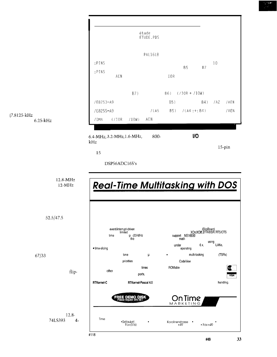
sample at slightly more than twice the
bandwidth of the input signal. Since
the clock rate alters the pass-band
frequency of the brick-wall filter, the
likelihood of aliasing the input signal
is very small. If you simply “throw
away” data to simulate a lower
sampling rate, the likelihood of
aliasing increases. Presumably, the
reason one would desire a lower
sampling rate is to diminish the data
storage requirement. Throwing away
data is still possible via software, as
long as you understand the implica-
tions of possibly violating the Nyquist
limit.
Although Motorola specifies a
minimum clock frequency of 1 MHz
conversion rate), I have
included the
conversion rate
because it was available “free.” Even
though, the SNR specification suffers,
you may find this acquisition rate
useful. This is also true for clock rates
higher than 12.8 MHz supplied via the
external input. We have experimented
with frequencies higher than 20 MHz.
Again, the SNR suffers, but the data
may still prove useful.
Similarly, please note that there is
nothing magical about a
oscillator. For example, a
oscillator would result in acquisition
rates about 6% lower than those
quoted in Table 1.
Preliminary data provided by
Motorola indicated that a worst-case
clock symmetry of
was
allowed. I found this curious since
their example circuit, which showed a
simple crystal/inverter oscillator, was
extremely unlikely to provide symme-
try that tight. Motorola has since eased
that specification to allow for a clock
symmetry of
ratio. (Point of fact:
A simple method of obtaining excel-
lent symmetry is to start with twice
the desired frequency and use a
flop to divide by two.) What’s more
important than clock symmetry,
however, is a low-jitter clock source.
Generally, ready-made 4-pin oscilla-
tors exhibit lower jitter than ones built
from a crystal and inverters.
The various acquisition rates are
generated by dividing down a
MHz oscillator via a
dual
bit ripple counter (US). U5 produces
Listing l-Board
decoding is simplified by using a PAL instead of discrete logic.
TITLE
ADDRESS DECODER
PATTERN
REVISION
(PRODUCTION VERSION)
DATE
APRIL 7, 1989
CHIP
ADDRESS-DECODE
1
2
3
4
5
6
7
8
9
A9 A8 A7 A6 A5 B4 B6
GND
11 12
13
14
15
16
17
18
19
20
E8253 A4
A2 IOW
COMP E8255 DMA VCC
EQUATIONS
COMP
= /(A7 :+:
* /(A6 :+:
*
* /A8 * COMP * /(A5 :+:
* /(A4 :+:
*
*
* /A8 * COMP *
:+:
*
*
A2 *
=
+
+
and
EXTERNAL
square waves at its QA, QB, QC,
Access to the signals listed on the
and QD outputs, respectively. U4, a
next page is provided via a
74F 1 multiplexer, is used to select
female D-shell connector. Where
the appropriate clock rate and present
applicable, the signal levels are TTL
it to the
clock input.
compatible.
for Microsoft C, Borland C, Borland/Turbo Pascal
Develop Real-Time Multitasking Applications under MS-DOS with
RTKernel!
RTKernel is a professional, high-performance real-time multitasking kernel. It runs under
MS-DOS or
in
ROM
and supports Microsoft C, Borland Ctt, Borland/Turbo Pascal, and Stony Brook Pascal+. RTKernel is a
library you can link to your application. It lets you run several C functions or Pascal procedures as parallel
tasks. RTKernel offers the following advanced features:
l
preemptive,
scheduling
l
supports up to 36COM ports
Hostess boards)
l
number of tasks only
by available RAM
l
supports protocols
l
task-switch
of approx. 6 s
486)
l
full
of
UART chip
l
performance is independent of number of tasks
l
supports
coprocessor and emulator
l
use up to 64 priorities to control your tasks
l
fast, inter-networkcommunication
Novell’s IPX
l
priorities changeable at run-time
l
runs
MS-DOS 3.0 to
DR-DOS,
can be activated
or without
system
l
programmable timer interrupt rate (0.1 to 55 ms)
l
DOS calls from several tasks without re-entrance problems
l
high-resolution timer for
measurement (1 s)
supports resident
applications
l
activate or suspend tasks out of interrupt handlers
l
runs Windows or DOS Extenders as a task
l
programmable interrupt
l
supports
and Turbo Debugger
l
semaphores, mailboxes, and message-passing
l
Kernel Tracer for easy debugging
l
keyboard, hard disk, and floppy disk idle
l
usable by
tasks
l
full source code available
l
interrupt handlers for keyboard, COM
and
l
no run-time royalties
network interrupts included with source code
l
free technical support by phone or fax
4 . 0 $495
$ 4 4 5
International orders: add $30 shipping and
C Source Code: add $445
Pascal Source Code: add $375
Mastercard, Visa, check, bank transfer accepted.
Professional Programming Tools
In North America,
please
contact:
Outside North America, please contact:
On
Marketing
On Time Marketing
88 Christian Avenue
NY 11733 USA
32 20357 Hamburg GERMANY
Phone (516) 689-6654.
689-l 172
Phone
40 43 74 72
40 43 51 96
CompuServe 73313.3177
CompuServe 100140,633
The Computer Applications Journal
issue
August 1994
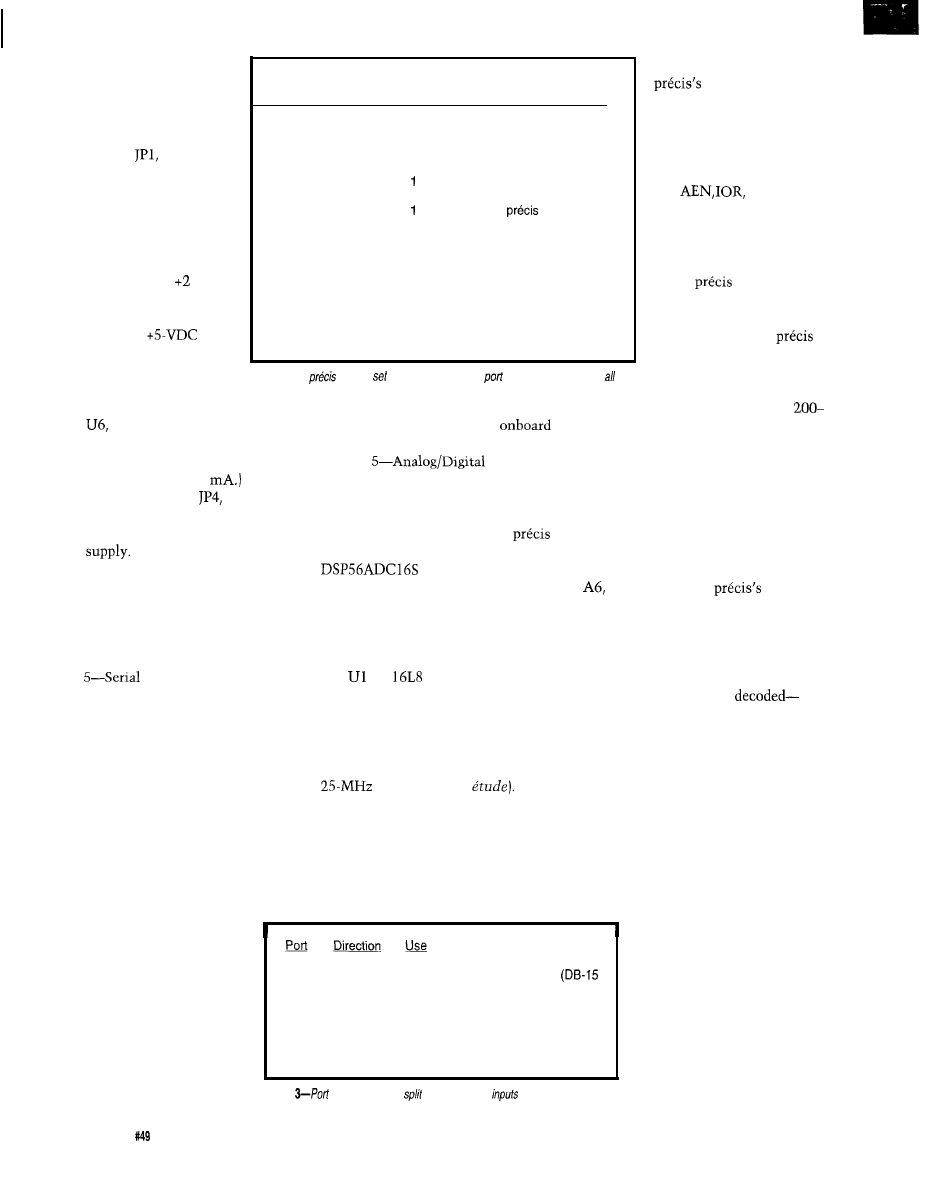
Pin l-External Reference
In/Out: Permits you to
monitor the 2-v
reference built into the
ADC. By removing
jumper
an external
voltage reference may
be injected on this pin.
This facilitates using a
more precise reference
or simply a different
reference voltage
(maximum of
VDC).
Pin 2-Analog Supply In/
Out: The
analog supply to the
ADC. It is isolated
from the PC’s switch-
ing power supply by
Base Address
Jumper Settings
Hexadecimal
A7 A6 A5 A4
Possible Conflict
200
0
0
0
0
Game port
210
0
0
0
1
Expansion unit
220
0
0
1
0
Reserved by IBM
230
0
0
1
1
Reserved by IBM
240
0
0
0
Reserved by IBM
250
0
1
0
1
260
0
1
0
factory setting
270
0
1
1
1
LPT2
280
1
0
0
0
290
1
0
0
1
2A0
1
0
1
0
2B0
1
0
1
1
2co
1
1
0
0
2D0
1
1
0
1
2E0
1
1
1
0
2F0
1
1
1
1
COM2
Table
2-The
may be up for any of 16 base
addresses, though not
potential addresses are without conflict.
a 3-terminal regulator. You
may use Pin 2 to provide power to
external circuitry. (Maximum
current draw is 200
By
removing jumper
the ADC
may alternatively be powered
from an external, linear power
Pin 3-Serial Clock Out: Comes
directly from the ADC. It is not
buffered.
Pin 4-Frame Sync Out: Comes
directly from the ADC. It is not
buffered.
Pin
Data Out: Comes
directly from the ADC. It is not
buffered.
Pin 6-General-Purpose TTL Input:
Software accessible via port PC6
in the 8255.
Pin 7-General-Purpose TTL Output:
Software accessible via port PC3
in the 8255.
Pin 8-External Clock In: If used, this
input must be a TTL-compatible
square wave. It is directed to the
74LS 15 1 and is selected via
software as mux channel
this by comparing the
Base Address Select
Jumpers with the PC’s
corresponding address
lines. This occurs in
parallel with decoding the
PC’s I/O signals A9, A4,
A2,
and IOW,
according to the equations
found in Listing 1.
Alterability of the base
address allows you to
locate
at any one of
sixteen base addresses and
permits multiple boards in
one computer. The
board occupies four I/O
port locations and may be
mapped into specific base
addresses in the range
accuracy clock than the
oscillator(s).
Pins 9-l
Ground.
Note: Since the SCO, SDO, and
FSO signals are available at this
connector, it is possible to use
as an evaluation platform for the
even without a PC.
Just remember to tie the appropriate
mux select lines to provide a clock
source.
ADDRESS DECODING
is a
PAL. Although this
PAL provides more functionality than
is required, it is used in another ADC
board we manufacture (see
Circuit
Cellar INK
issues 13 and 15 for
construction details regarding an 8-bit,
digitizer called
A
JEDEC fuse map for this PAL is
available on the BBS if you would
prefer not to work with the PALASM
source code.
The PAL’s job is to generate a
chip-select signal for the 8255. It does
2F0 hex (see Table 2). A read from or
write to I/O space is “in range” when
the following conditions are met:
1) address line A9 is high and A8
is low. This corresponds to a hexadeci-
mal base address whose most-signifi-
cant digit is 2.
2) the next-most-significant hex
digit is determined by comparing A7,
A5, and A4 with
Base
Address Select jumpers.
3) the least-significant hex digit is
always zero. When A2 is high, the
8255 is selected. Specific registers
within the 8255 are accessed by Al
and AO. Note: A3 is not
therefore the Base Address + 8 is
redundant.
BUS INTERFACE
Interface to the system data bus is
via U2, an 8255 programmable
peripheral interface. Although some
engineers do not advocate attaching
NMOS LSI devices directly to the
system bus, I have reliably used the
method in several products. The
advantage of connecting the
8255 directly to the bus is
D7. It becomes the
master clock for the
General-purpose output (DB-15 pin 7)
12.8-l MHz may be used
PC2
output
M
UX
S2 (timebase select)
loading limit of two LSTTL
PC1
output
M
UX
Sl (timebase select)
loads).
to
acquire data at a rate
PC0
unavailable internally or
output
M
UX
SO (timebase select)
The 8255 is mapped into
,
four locations in the PC’s I/O
to use a higher-stability/
Table
C on the 8255 is
between status
and control outputs.
space. Port A is assigned as
34
Issue
August 1994
The Computer Applications Journal
the converter’s least-significant byte.
Port B is assigned as the converter’s
most-significant byte. Port C is split
into an input nybble and an output
nybble. Bits 7-4 are “read-only,”
whereas bits 3-O are “write-only.”
Since it is not possible to perform
nybble-wide I/O operations, a full 8
bits must be read from, or written to,
an I/O port. Writing an 8-bit value to
port C has no effect on its read-only
portion. Likewise, when reading an
bit value from port C, bits 3-O are
undefined. Individual bit definitions
for port C are given in Table 3.
PCB
Although the digital portion of
this design can, for the most part, be
implemented in wire wrap, the analog
portion requires a great deal more care.
Originally, I prototyped the ADC and
analog circuitry “dead bug style” over
a copper ground plane. I made all
component leads as short as possible
and the circuit performed well.
However, the first version of the
did not work properly. A trace
slightly over
inches long connected
the ADC (U3) clock input to the mux
(U4) output. This proved to be too long
for the edge-rate involved. Although I
found several solutions to the problem,
the simplest was to replace the
with a
and replace the
PCB trace with a piece of
75-Q coax.
In the second version of the PCB, I
decided that changing the chip layout
to position U4 extremely close to U3
would have required more effort than I
cared for. Instead, I decided to etch the
transmission line directly onto
the PCB. Now, it is well known that
empirical formulas for fabricating
transmission lines in printed circuit
boards exist (see Motorola’s seminal
work, the ECL data book]. Unfortu-
nately-for two-sided boards at
these formulas are based on having an
“infinite” ground plane on the oppo-
site side of the controlled-impedance
trace. Since there was little room for
any sort of ground plane above the
trace, an “infinite” one was out of the
question.
Fortunately, I found an easy
solution. A friend of mine had recently
PAL
GAL
EPROM
EEPROM
FLASH
MICRO
etc..
Free software updates on BBS
Powerful menu driven software
up to 128 Channels
up to 400 MHz
up to 16K Samples/Channel
Variable Threshold Levels
8 External Clocks
16 Level Triggering
Pattern Generator Option
LA12100 (100 MHz, 24 Ch)
LA32200 (200 MHz, 32 Ch)
LA32400 (400 MHz, 32 Ch)
LA64400 (400 MHz, 64 Ch)
Call (201) 808-8990
Link
369 Passaic Ave, Suite 100, Fairfield, NJ 07004 fax: 808-8786
HUGE BUFFER
FAST SAMPLING
SCOPE AND LOGIC ANALYZER
C LIBRARY W/SOURCE AVAILABLE
POWERFUL FRONT PANEL SOFTWARE
$1799
DSO-28204 (4K)
$2285 DSO-28264 (64K)
DSO Channels
2 Ch. up to 100
1 Ch. at
4K or 64K
Cross Trigger with LA
125 MHz Bandwidth
Logic Analyzer Channels
8 Ch. up to 100 MHz
4K or 64K
Cross Trigger with DSO
The Computer Applications Journal
Issue
August 1994
3 5
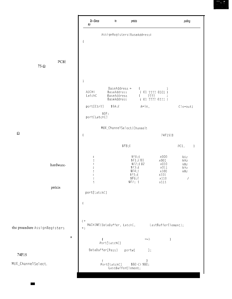
begun slinging code for a purveyor of
signal integrity software. My friend
convinced his boss to use their
software to solve for the impedance of
a PCB transmission line based on its
physical characteristics. Working
together, it took only a few iterations
before we specified the correct physi-
cal layout for a transmission line
(having both its signal and return
lines on the same side of the
which yielded a
differential
impedance.
Listing
using
interrupts
service
would require a great deal of overhead,
is the besf
way acquire data.
procedure
word);
8255 port Address
Definition
Direction
Port A
base + 4 ADC least significant byte
Port B
input
base + 5 ADC most significant byte
Port C
input
base + 6 Bits 7 3
status
Port C
input
base + 6 Bits 4 0
control
Control
output
base + 7 8255 mode register
not applicable
What we ended up with is prob-
ably best described as a two-dimen-
sional coaxial cable. The center
conductor was a 0.062” trace bounded
on either sided by a 0.022” shield trace
separated by a 0.008” space. The
artwork was created this way with the
expectation that after acid had etched
the board, there would be a 0.020”
ground trace, a 0.010” space, a 0.060”
signal conductor, another 0.010” space,
and finally a 0.020” ground trace. As I
recall, we couldn’t quite get down to
75 in the available space, but the
board worked beautifully nevertheless.
When passed the Base Address, this procedure sets the global
addresses of hardware registers relative to the Base Address and
initializes the 8255
begin
ADCLo
:=
4; 01 ???? 0100
:=
+ 5;
: =
+ 6; 01
0110
Ctrl
:=
+ 7;
:=
1001 1010
B=in, Chi=in,
BitsC :=
:= BitsC
end:
procedure
byte);
Direct a clock source to the ADC via the
begin
SOFTWARE
BitsC := BitsC and
1111 1000 MUX bits PCO,
PC2
Complete source code, in Pascal,
for a crude digital storage oscilloscope
can be found on the BBS. Listing 2
defines all of the crucial
specific routines. I chose to show the
examples in Pascal because it seemed
like a good compromise for those who
favor C and those who favor BASIC.
Acquiring data with
is
extremely simple. Programming
consists of three principal functions:
configuring the 8255, selecting a clock
source via the multiplexer, and reading
the ADC.
case Channel of
0
BitsC :=
BitsC or
DO = xxxx
6.25
1 BitsC := BitsC or
= xxxx
12.5
2 BitsC := BitsC or
= xxxx
25
3 BitsC := BitsC or
D3 = xxxx
50
4 BitsC := BitsC or
D4 = xxxx
100
5 BitsC := BitsC or
D5 = xxxx
User Osc.
6 BitsC := BitsC or
D6 = xxxx
User Osc. 2
7 BitsC := BitsC or
D7 = xxxx
External Clock
end;
:= BitsC
end:
This code fragment actually does all of the work.
When the PC is booted, all 8255
ports are set to the high-impedance
state. This protects the hardware until
can
configure the 8255. Writing 9A (hex) to
the 8255’s control port (Base Address
7) configures the 8255 properly.
The commented-out code shows how to call the assembly language
subroutine which performs the same function, albeit faster.
ADCLo,
Pass := 0:
repeat
A clock source is selected by
writing the appropriate bit pattern to
the
1 multiplexer through port
C. This is detailed in the procedure
The application program must
have access to the data whether it is
repeat Wait for PC7 to go HI
vaid data
until
and $80 = $80;
:=
ADCLo
inc (Pass);
repeat Wait for PC7 to go low
until
and
until Pass =
3 6
Issue
August 1994
The Computer Applications Journal
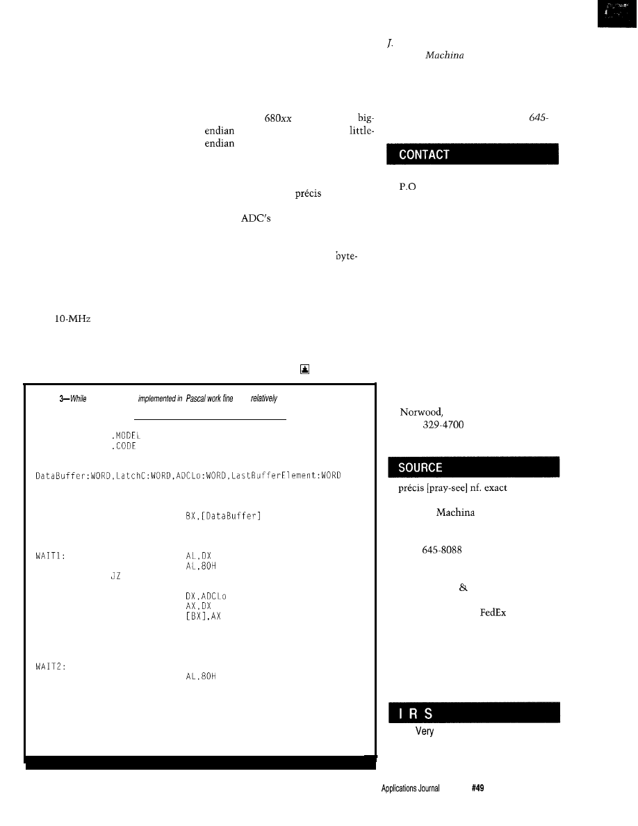
processed in real time or stored in a
buffer. Since the overhead required to
perform 100,000 interrupts per second
would be extremely high, the code
fragment shown in Listing 2 simply
polls the ADC until a valid word is
available. Each time the converter’s
Data Ready flag (hardware signal called
Frame Sync Out) goes high, a valid
word exists at the shift register’s
outputs. A new value is latched each
time Data Ready goes high, and this
value must be read in real time. To
prevent rereading the same value
because Data Ready was still high after
that value had been processed, it is
necessary to wait for Data Ready to go
low before reading the next valid word.
Another way to think of this is that
the polling routine must be “edge”,
rather than “level” sensitive.
The Pascal implementation works
fine on
80286 O-wait-state [or
faster) machines. Slower machines will
require an assembly language subrou-
tine like the Pascal-specific one shown
in Listing 3.
Finally, it is well known that Intel
processors use a byte-swapped memory
architecture. The architecture is often
called “little-endian” because it
employs both reverse byte ordering
and reverse bit ordering. By contrast,
the Motorola
architecture is
with respect to bytes, but
with respect to bits. However,
it is perhaps less well known that
80x86 processors follow the Motorola
scheme as far as I/O operations are
concerned. As far as
is con-
cerned, that’s why the 8255’s port A
gets the
LSB and port B gets the
MSB.
Reiterating, although 16-bit data is
stored in the PC’s memory in
reversed order, 16-bit data read from
and written to I/O ports is not. This
means for I/O operations, the lower
(numeric) address byte contains the
least-significant data byte in a 16-bit
word.
So start building that board,
downloading that software, and
collecting some data.
Listing
low-/eve/routines
on
fast
machines,
slower
ones
require fhe use of assembly language.
TPASCAL
Machine
PROC
FAR
Machine
CODE
PUBLIC
MOV
MOV
MOV
IN
AND
MOV
IN
MOV
INC
INC
MOV
IN
AND
JNZ
LOOP
RET
ENDP
ENDS
END
Machine
CX,LastBufferElement
DX,LATCHC
WAIT1
BX
BX
DX,LATCHC
AL,DX
WAIT2
WAIT1
Conrad Hubert is a principal in
Deus Ex
Engineering Inc.,
where he provides consulting services
for the development of hardware and
software for embedded systems, data
acquisition, and digital signal process-
ing. He may be reached at (612)
8088.
Motorola, Inc.
Box 20912
Phoenix, AZ 85036
Crystal Semiconductor Corp.
4210 S. Industrial Dr.
Austin, TX 78744
(512) 445-7222
Fax: (512) 455-7581
Texas Instruments, Inc.
9301 Southwest Fwy.
Commerce Park, Ste. 360
Houston, TX 77074
(713) 778-6592
Analog Devices
One Technology Way
P.O. Box 9106
MA 02062-9 106
(617)
Fax: (617) 326-8703
Deus Ex
Engineering, Inc.
1390 Carling Dr., Ste. 108
St. Paul, MN 55108
(612)
Fax: (612) 645-0184
1. Assembled tested board with
source code in C, BASIC, and
Pascal (includes
economy
shipping) . . . . . . . . . . . . . . . . . . . $354.00
2. Printed circuit board only
(includes Priority Mail shipping)
. . . . . . . . . . . . . . . . . . . . . . . . . . . . . . . . . . . . . . . . . . $99.00
Visa and Mastercard accepted.
404
Useful
405 Moderately Useful
406 Not Useful
The Computer
Issue
August 1994
3 7
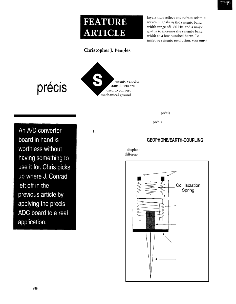
Calibrating
Seismic
Velocity
Transducers
with
motion into an electrical signal.
Exploration geophysicists use these
devices to sense seismic wave energy
that has been reflected and/or refracted
off layers within the earth’s interior. A
seismic velocity transducer, more
commonly known as a geophone
(Figure will generate a voltage that
is proportional to the rate at which the
ground displacement changes with
time (i.e., it senses the ground’s
begin with a better understanding of
the sensing device used to record
seismic waves.
For the research of my Master of
Science thesis at Texas A&M Univer-
sity, my advisors and I developed the
theory and a prototype system for
calibrating geophones in situ. Using
parameters derived from the calibra-
tion process, I can model the broad-
band amplitude and phase response for
a planted geophone when it acts as a
seismic wave sensor. I present here a
brief description of the geophone/
earth-coupling phenomenon and how I
used the
analog-to-digital data
converter card
(see
the article describ-
ing
starting on page 28 of this
issue) to measure a geophone’s broad-
band amplitude and phase response.
PHENOMENON
velocity and not the ground’s
Early seismic explorers noted that
ment). Inside the geophone,
at high frequencies
(100
Hz and above),
tial motion between a
spring-suspended coil and
a fixed magnet generates
the voltage that is
Geophone
proportional to the
Terminals
ground motion. This
electrical signal is then
digitized and recorded for
later processing. Using
data from an array of
these sensors, geophysi-
cists process the data to
Sensor Coil
enhance and identify
subsurface features that
may contain oil and gas.
Permanent
Basic to exploration
Magnet
seismology is the need
for improved seismic
resolution of deeper
Geophone Case
Figure 1-A geophone, or seismic
velocity transducer, generates a
voltage that is proportional to the
rate at which the ground displace-
ment changes with time.
Plant Spike
3 8
Issue
August 1994
The Computer Applications Journal
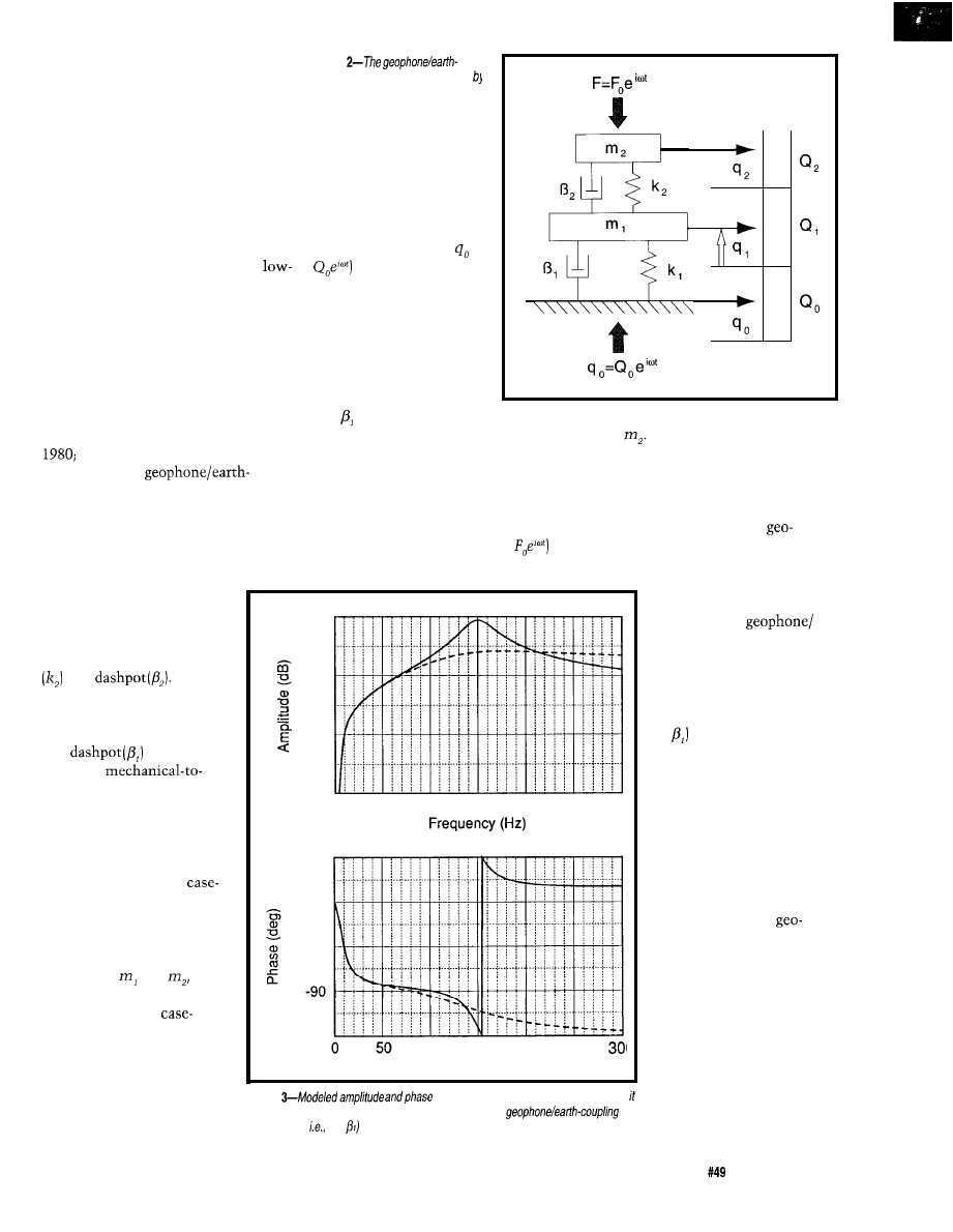
the motion of the geophone did not
necessarily follow the ground motion
of the earth itself, and they attributed
the causes of these departures to
coupling effects between the geophone
and the earth. Poor coupling results
when the geophone’s plant spike fails
to develop good cohesion between it
and the soil in which it is planted (as
happens when planted in loose sand).
This effect causes a high-frequency
resonance, which in turn acts as a
pass filter limiting seismic resolution
at frequencies above the coupling-
related resonant frequency. In firmer
soils, where the cohesion between the
geophone and the soil are good,
coupling problems are not as apparent
(Krohn, 1984).
Figure
coupling behavior can be modeled
a compound harmonic oscillator
system.
from the ground direction
by simple harmonic
ground displacement ( =
yields the predicted
geophone response to a
seismic impulse (see
graphs in Figure 3). The
solid line represents a
poorly coupled situation
where the coupling effect
is underdampened (i.e., a
low value), while the
dashed line shows a better-damped
condition indicating somewhat better
coupling between the geophone and
the earth.
Several studies (e.g., Washburn
and Wiley, 1941; Hoover and O’Brien,
and Krohn, 1984) have demon-
strated that the
coupling phenomenon resembles a
damped resonant system that can be
modeled using a system of two simple
harmonic oscillators stacked in series
(i.e., a compound harmonic oscillator,
see Figure 2). The smaller
mass (m,) represents the
geophone coil coupled to the
geophone magnet and case
assembly (m,) by a spring
and
The
coupling of the geophone to
the earth is described using
an additional spring (k,)
and
combina-
tion. The
electrical transfer of energy
(geophone transduction) is
assumed linearly propor-
tional to the velocity
difference between the
geophone coil and the
mounted magnet.
A very different response becomes
apparent (Figure 4) when a simple
harmonic forcing function (F =
is
applied to the modeled geophone’s
40
20
0
-20
mass,
In this case, we are modeling
the application of an electrical impulse
to the geophone coil, assuming a
bidirectionally linear electromechani-
cal system. The peak amplitude
response corresponds to the
phone’s own resonant frequency (10
Hz), while at the coupling response
frequency (150 Hz), a notch
appears. This notch is
caused by the
earth-coupling effect,
where it acts as a mechani-
cal vibration damper.
Higher degrees of damping
(that is, increased values
of mitigate this me-
chanical vibration damper
effect, making it unappar-
ent.
0
50
100
150
200
250 30
180
90
The amplitude and
phase response for the
differential motion between
the masses, and
corresponding to the
geophone coil and
mounted magnet, respec-
tively, is dependent on how
the mechanical system is
driven. Solving the differen-
tial equations for the case
where the system is driven
0
-180
100
150
200
250
Frequency (Hz)
Figure
response of a geophone for the case when
is driven by simple harmonic ground motion for both poor
(solid curves,
low and good coupling (dashed curves).
CALIBRATION SYSTEM
DESIGN
The geophone calibra-
tion system I developed is a
prototype, designed prima-
rily for testing my
phone/earth-coupling
theory. I chose to develop
the calibration system
using an off-the-shelf
technological approach by
fitting my 80286 MS-DOS
personal computer with a
digital data acquisition
card. In selecting a data
acquisition card for this
project, I had to overcome
The Computer Applications Journal
Issue
August 1994
3 9
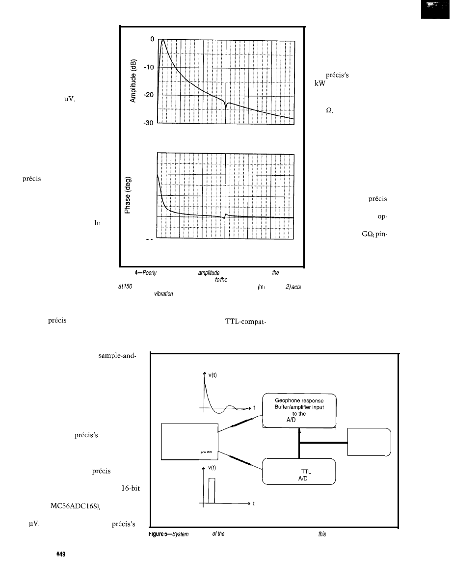
many of the problems
common to engineering, the
primary being price versus
performance. For my
research, I needed a data
acquisition card with
16
bits dynamic resolution and
a least-single-bit resolution
of around 50
To
determine the geophone’s
response at high frequencies
(a maximum of approxi-
mately 500 Hz], I needed to
do data sampling at about
2000-4000 samples per
second (Sps).
I ended up selecting the
data acquisition card
because it met several of the
design criteria, and it
offered several features that
eased the development of
the calibration system.
addition to that card, the
calibration system also
included a battery-powered
external unit that functions
as a high-input-impedance
buffer/amplifier and a
calibration pulse amplitude
controller. The calibration
system is schematically
shown in Figure 5.
Figure
coupled geophone
and phase response for case when
a simple harmonic forcing function is applied geophone coil. The trough located
Hz is caused by coupling behavior, where the lower mass in Figure
as a mechanical
damper.
The
board solved several
calibration system design problems.
First, the card acquires data using
sigma-delta modulation, which
180
90
0
-90
-180
0
50
100
150
200
Frequency (Hz)
250
300
0
50
100
150
200
250
300
Frequency (Hz)
TTL output port to provide
the pulse function (dis-
cussed below) to the
geophone under test.
The only drawback in
the
design is its 2
input impedance.
Because a geophone has a
nominal impedance of 250-
300 this low-valued
input impedance may
adversely distort the
geophone’s transient
response by excessively
damping the geophone. To
increase the input imped-
ance, I placed an Analog
Devices AD524 instrumen-
tation op-amp between the
geophone and the
signal input (Figure 6, upper
portion). I chose this
amp because it has an input
impedance of 1
selectable gains of 1, 10,
100, 1000; and it has a flat
response from DC to 1000
Hz-well above the band-
width of interest for
calibrating geophones.
During the calibration tests,
available through a DB-
15
female
connector, among them
ible general-purpose input and output
ports. The calibration system uses the
the transient response
(signal-to-noise ratio) of the geophone
tested was sufficiently strong to only
need the AD524 as a unity-gain
amplifier.
eliminates the need for a
hold amplifier and an antialias filter.
Data sampling rates are software
Geophone Response
Geophone
to be in situ
calibrated
selectable at 12500, 25000, 50000, and
100,000 Sps, with the cutoff frequency
located at 45.5% of the chosen
sampling rate. Even though my
bandwidth of interest for calibrating
Board
geophones isl-500 Hz, the cutoff
frequency for the
slowest data
Analog-to-digital
Conversion Board
acquisition rate of 12500 Sps is still
mounted in
above 5000 Hz and, therefore, did not
MS-DOS Computer
affect my measurements.
Signal input to the
is via a
BNC connector and can have a range
of -2 to 2 V, and because it has a
analog-to-digital converter (i.e., the
Motorola
it has a
Pulse controller/limiter
driven by
on
board the
Board
t
least-significant-bit resolution (LSB) of
Calibration Pulse
61
Also incorporated into
design are several external connections
schematic
geophone calibration system developed for
research.
4 0
Issue
August 1994
The Computer Applications Journal
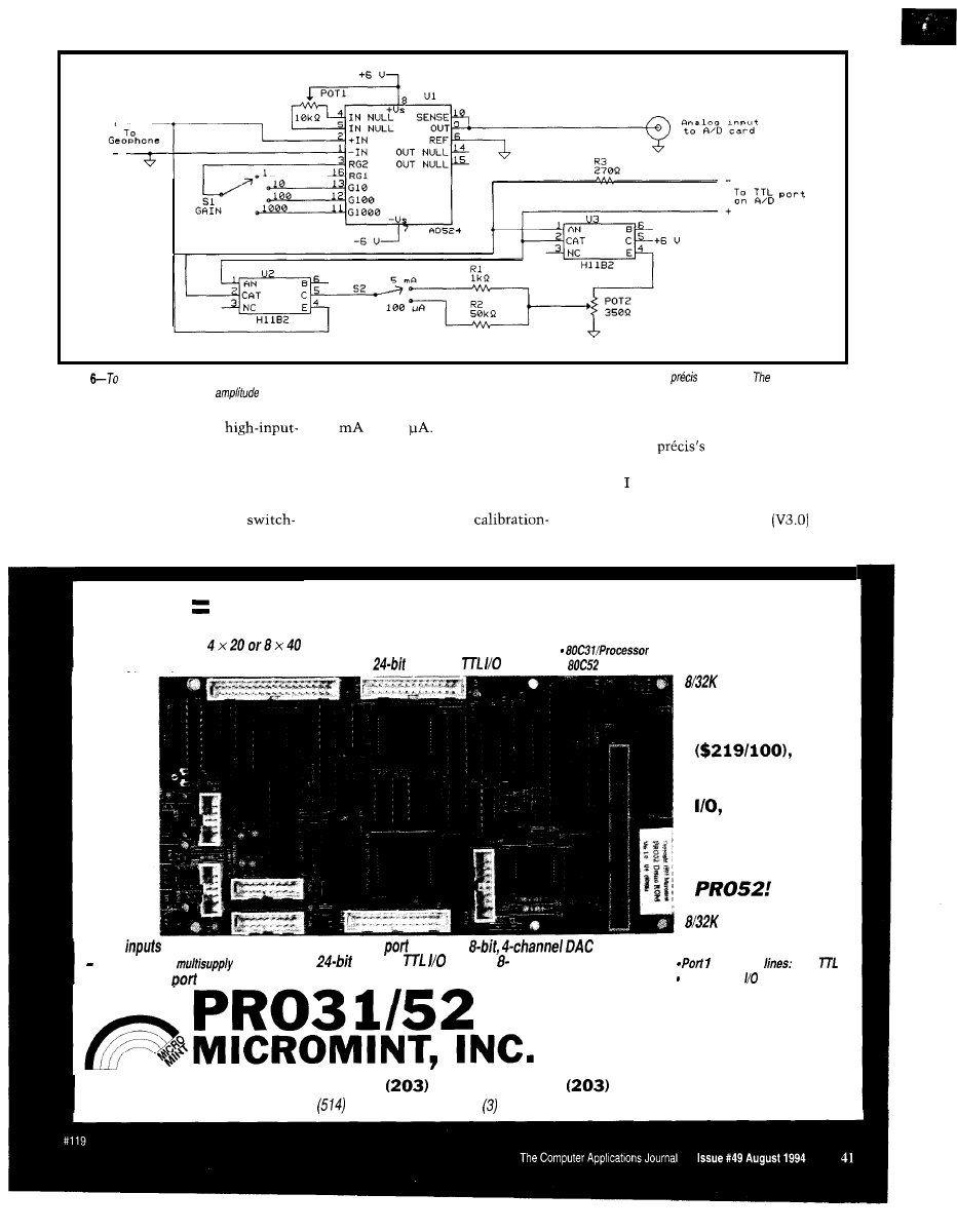
c a r d
Figure
increase the input impedance, an Analog Devices
AD524 instrumentation op-amp
is used between the geophone and the
signal input.
external unit
a/so functions as a calibration-pulse
controller.
In addition to being a
5
or 100
The two different
acquisition and control software to
impedance amplifier, the external unit
current supplies were originally
cycle the
TTL output port on
also functions as a calibration-pulse
intended so the calibration system
and off.
amplitude controller (Figure 6, lower
could be used to perform both impulse
accomplished software timing
portion). It limits the geophone’s
and step-pulse calibration testing
control for the calibration-pulse
calibration-pulse current to a
(discussed below). The
duration using the PCHRT
and-potentiometer maximum of either
pulse signal is generated using the data
High-resolution Timer Toolbox by
PRO Positively Rampant Optimization
CMOS PROCESSORS
Hardware real-time
clock
or
4 x 5 keypad input
LCD
display output
parallel
l
with BASIC52
RAM
PRO31 prices start
as low as $289
includes SK RAM,
watchdog, 56 bits
S-bit ADC,
and LCD interface.
And it only costs
$10
more for
ROM
Power
Auxiliary serial
EXPANSION HEADER
Single supply or
option
parallel
or lo-bit, &channel ADC
processor
B-bit
Console serial
Hardware watchdog
Six decoded address strobes
. Eight address lines
4 Park Street
l
Vernon, CT 06066
l
871-6170
l
Fax
872-2204
in
Europe: (44) 0285-658122
l
in Canada:
336-9426
l
in Australia: 467-7194
l
Distributor Inquiries
Welcome!
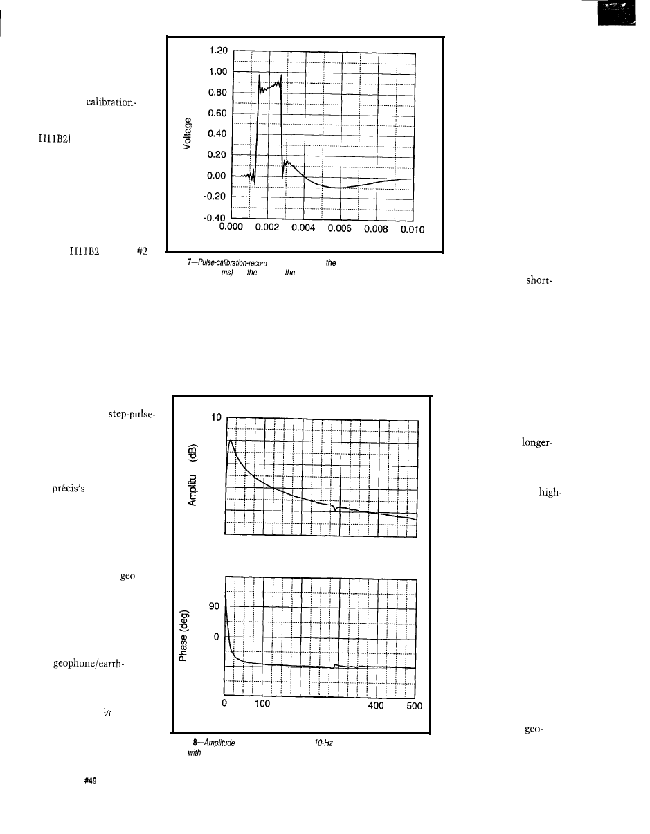
Ryle Design Inc. To
prevent damaging both
the ADC card and the
computer during the
calibration process,
I
passed the
pulse signal through a
optoisolator (Motorola
in the external
unit. Thus, the calibra-
tion-pulse current is
drawn from the external
unit’s battery power
supply (a pair of 9-V
batteries stepped down to
6 V) instead of the
computer. I added the
second
(labeled
in Figure 6) after the
initial testing of the
calibration system
Time (s)
Figure
beginning, showing applied calibration pulse (for a
pulse duration of2
and onset of geophone transient response.
Chapman et al. (1988)
demonstrate that impulse
calibration provides more
power at higher frequen-
cies, yielding an improved
signal-to-noise ratio for
the geophone’s transient
response. Ideally, a Dirac
delta function [a “spike”
of energy that has infinite
height and infinitesimal
duration) would be used to
impulse calibrate the
geophone. Physically, it’s
not possible to generate a
pure Dirac delta function,
but as Chapman et al.
(1988) show, a reasonable
approximation can be
made by using a
duration rectangular
function. In making the duration of
the rectangle function small, it has a
near flat spectral response over the
bandwidth of interest, and for all
intents and purposes can be looked
upon as a “bandwidth-limited” delta
function. A short-duration pulse offers
more energy at high
frequencies, at the expense
of a degraded signal-to-noise
ratio.
Conversely a
duration pulse delivers
more energy, increasing the
signal-to-noise ratio at the
expense of decreasing
frequency resolution.
Impulse calibrations were
done using a process similar
to that used for a step
calibration, except
I
signifi-
cantly shortened the time
period the TTL port was
left. The data acquisition
software, as programmed,
allows for four different
pulse durations ranging
from 0.62 to 2 ms (I con-
trolled pulse duration
timing using the PCHRT
software that I discussed
above). Initial testing
revealed that pulse dura-
tions of l-2 ms are suffi-
cient for analyzing
phone/earth-coupling
behavior. Calibration
revealed there was an additional
inadvertent path to ground, causing
unwanted additional damping of the
geophone’s transient response.
CALIBRATION THEORY,
PROCEDURE, AND RESULTS
The calibration system
as developed is capable of
performing both
and impulse-type calibra-
tions. Step-pulse calibra-
tions are performed by using
the data acquisition and
control software to switch
the
TTL output port
on, and then waiting a few
seconds for the geophone to
stabilize before switching
the TTL output port off.
After switching off the TTL
output port, the software
starts recording the
phone’s transient response.
Step-pulse calibrations were
performed in the initial
testing of the calibration
system, but were not
included on the research
into
coupling because this
technique limits resolution
at higher frequencies. A
step-pulse has a amplitude
decay with increasing
the geophone’s transient response,
the high-frequency resolution is
severely impaired [Chapman et al.,
1988). Using an impulse-type of
calibration permits better resolution
of a geophone’s high-frequency
response.
frequency, and when passed
through a convolution with
0
8
-10
-20
-30
-40
0
100
200
300
400
5oc
Frequency (Hz)
1 8 0
- 9 0
- 1 8 0
2 0 0
3 0 0
Frequency (Hz)
Figure
and phase response for a
geophone planted in loose
sand,
a poorly damped coupling-related resonance located at 288 Hz.
4 2
Issue
August 1994
The Computer Applications Journal
system tests also revealed that a
recording period of five times the
natural resonance frequency of the
geophone under test (e.g., 0.5 for a
geophone) proved to be ample.
Longer recording periods only served
to incorporate additional noise.
A major concern about the
calibration process is the coordination
of the onset of data acquisition with
the end of the applied calibration
pulse. The data acquisition software
starts the calibration procedure by first
turning the TTL output port on, and
then waiting the specified duration
before switching it off. After that, data
acquisition commences. Any delay
between the two actions would cause
an error in the amplitude and phase
determination. As it turns out (rather
serendipitously), this is not a problem
because the optoisolators (two
torola
used in the external
unit have a slow response and cause an
approximate
delay. The data
acquisition software executes faster
and is capable of recording the calibra-
tion pulse in addition to the geophone
transient response (Figure 7). Prior to
determining (i.e., Fourier transforming)
the geophone’s amplitude and phase
response to the calibration pulse, the
pulse is deleted from the recorded data.
The ringing in the calibration pulse is
possibly by either Gibb’s phenomenon
caused by the digitization of the pulse
by the
or some artifact caused
by the optoisolators.
I
calibrated a variety of geophones
with different natural resonance
frequencies under similar conditions
to examine their
coupling behavior. The geophones I
used for testing the calibration theory
and system consisted of ones with
natural resonance frequencies of 10,
40, and 100 Hz.
Planting the geophones in a large
bucket of loose sand and performing
the calibration tests as described above
revealed a coupling-related resonance
in the vicinity of 285 Hz for the three
geophones tested. Figure 8 shows the
amplitude and phase response for the
geophone with its coupling
resonance located at 288 Hz. Each
geophone has a slightly different
coupling resonance frequency because
of small differences in mass between
the geophones.
I
also performed calibration tests
on the same geophones when they
were planted in soils that were
significantly more consolidated.
Because of the greater cohesion
between the geophone plant spike and
the soil, the dampening was greater
and the coupling phenomenon was not
as pronounced and, thus, not observ-
able.
CONCLUSION
I
developed the calibration theory
and system presented here to gain a
better understanding of a geophone’s
in situ amplitude and phase behavior
and the deleterious effects caused by
geophone/earth-coupling. Based on a
better understanding of these effects,
exploration geophysicists can predict
and adjust their seismic surveying
practices to mitigate these effects. The
calibration system design is probably
not optimal, but it did succeed in
demonstrating and proving the theory
developed for describing the phenom-
enon.
The
data acquisition card
performed admirably throughout the
project, recording accurate and precise
measurements of each geophone’s
transient response to a calibration
pulse. The only drawback in using the
is that its slowest data sampling
rate is 12,500 Sps, which yields a
cutoff frequency well above 5000 Hz,
and well above any frequency relevant
to seismic exploration (approximately
l-500 Hz).
The external amplifier/pulse
controller could have been designed for
better performance, but given the time
and monetary constraints present at
the time, it was sufficient. For the
most part, this project is a success
because it did establish and demon-
strate the theory on
coupling (in addition to contributing to
the completion of my Master of
Science research).
Special thanks to my thesis research
advisors, Drs. Steven H. Harder and
Anthony
and to Conrad
Hubert of Deus Ex
Engineer-
ing Inc.
Christopher Peoples is presently a
part-time community college physics
instructor in Southern California. In
addition to his obvious interests in
geophysical data acquisition and
processing, he is also interested in
industrial process control and auto-
mation. He may be reached at
Chapman, M.C.;
and
Bollinger, G.A., 1988, “A
procedure for calibrating short
period telemetered seismo-
graph systems”: Bull. Seis.
Am., 78, no.
2088.
Hoover, G.M. and O’Brien, J.T.,
1980, “The influence of the
planted geophone on seismic
land data”: Geophysics, 45, no.
8, 1239-1253.
Krohn, C.E., 1984, “Geophone
ground coupling”: Geophysics,
49, no. 6, 722-731.
Menke,
Shengold, L.;
Hongshen,
Ge,
and
Lerner-Lam, A., 1991, “Perfor-
mance of the short period
geophones of the IRIS/
array”:
Seis.
Am., 81, no. 1, 232-242.
Washburn, H. and Wiley, H.,
1940, “The effect of the
placement of a seismometer
on its response characteris-
tics”: Geophysics, 6, 116-13 1.
Timer Toolbox
Ryle Design, Inc.
P.O. Box 22
Mt. Pleasant, MI 48804
(517) 773-0587
Deus Ex
Engineering, Inc.
1390 Carling Dr., Ste. 108
St. Paul, MN 55108
(612) 6458088
Fax: (612) 645-0184
407
Very Useful
408 Moderately Useful
409 Not Useful
The Computer Applications Journal
Issue
August 1994
4 3
Barry Rein, Esq.
Copyrights and Patents
for Protecting Software
Recent Progress in Finding
the Proper Balance
0
he last year has
seen significant
developments in both
copyright and patent law
since both were made applicable to
computer software at the beginning of
the last decade. In 1992, Computer
Associates v. Altai in the Second
Circuit and Brown Bag Software v.
Symantec Corp. in the Ninth mark-
e d l y r e d u c e d t h e s c o p e g i v e n s o f t w a r e
copyright, specifically rejecting the
overly broad brush of
Whelan v.
as “too facile.” Significantly, Apple v.
Microsoft and Hewlett Packard (also
with the Ninth Circuit) adopted a
similar approach to user interfaces.
However, with Lotus v. Borland in the
First Circuit, which seemed to be
following a similar approach, we were
taken a step backward. In this case,
Judge Keeton held that Lotus’s macro
language is protectable by copyright,
and that Borland’s use of it was an
infringement. Keeton’s judgment is
now awaiting decision by the First
Circuit where it was heard by a panel
including soon-to-be Justice Breyer.
Although the court’s position on
infringement has developed, it is still
not without surprises. Within the last
few years, Sega Enterprises Ltd. v.
Accolade Inc. in the Ninth Circuit and
Atari Games Corp. v. Nintendo of
America Inc. in the Federal Circuit,
interpreting Ninth Circuit law, have
established a right under copyright law
to decompile or reverse engineer
software to extract ideas and related
elements which cannot be protected to
produce non-infringing products. In
1992, Arrhythmia v. Corazonix lent
greater rationality to the law on when
software constitutes statutory subject
matter for a patent. However, the law
is not free of mysterious anomalies as
this year’s In re Schrader indicates.
The net result is that we are much
closer to relegating the patent and
copyright regimes to their proper
constitutional roles, undoing the
damage done principally by the
inability of the patent system to
embrace the new science of software
in a timely fashion. We have come a
long way, finally closing in on where
we should have been at the outset.
COPYRIGHT PROTECTION
FOR SOFTWARE
The current analytical framework
for evaluating the scope of protection
for software by the copyright law is
best set forth in Computer Associates
v. Altai
decided June 22, 1992 and
amended December 17, 1992. Com-
puter Associates developed specific
applications which could run on a
number of different operating systems
through the use of a so-called “adapter
module.” Rather than rewriting the
particular application to make it
compatible with each different
operating system, Computer Associ-
ates divided the application into two
parts, one constituting the application
proper and the other, the adapter
module, constituting the coupling
between the application and each
particular operating system. Thus, to
rewrite an application for a different
operating system, it was only neces-
sary to rewrite its adapter module.
Altai hired Arney, a Computer
Associates programmer, who suggested
that Altai also use adapter modules.
What he did not tell Altai, according to
the facts established at trial, was that
he had brought with him purloined
44
Issue
August 1994
The Computer Applications Journal
adapter code from Computer Associ-
ates and was using it to write the Altai
programs. Altai found this out when
Computer Associates brought suit, and
immediately stopped selling the
accused programs. However, Altai
then rewrote the programs from
unprotected functional specifications
using programmers who were not
privy to Computer Associates code.
Altai admitted that its first version of
the programs was an infringement of
Computer Associates’ copyright, but
denied that its second “clean room”
version infringed.
The case establishes a model
for understanding the various levels
within software and software
development which lends itself to
copyright analysis. I will summa-
rize the bulk of the court’s model
which, by the way, the court said
was not applicable to categorically
distinct works such as screen
displays:
The Copyright Act defines a
computer program as “a set of
statements or instructions to be
used directly or indirectly in a
computer in order to bring about a
certain result” (17 U.S.C.
101). In
writing these directions, the courts
presume that a programmer works
“from the general to the specific.”
The model begins by identifying a
program’s ultimate function or
purpose. The model then maintains
that a programmer “decomposes” or
breaks the purpose down into “simpler
constituent problems or ‘subtasks’
which are also known as subroutines
or modules.” Sometimes, depending
on the complexity of its task, a
subroutine may be broken down
further into nested subroutines.
Having sufficiently decomposed
the program’s ultimate function into
its component elements, within this
model, a programmer then arranges
the subroutines or modules into
organizational or flow charts which
map the interactions between modules
which achieve the program’s end goal.
To accomplish these intraprogram
interactions, a programmer must
carefully design each module’s para-
meter list. According to expert Dr.
Randall Davis, appointed and fully
credited by the district court, a para-
meter list is “the information sent to
and received from a subroutine.” The
parameter list also includes the form
in which information is passed
between modules and the informa-
tion’s actual content. The courts
recognize that interacting modules
must share similar parameter lists so
that they are capable of exchanging
information.
According to the model, “The
functions of the modules in a program
together with each module’s
q
We are much closer
to relegating the patent
and copyright regimes
to their proper cons
tional roles, undoing the
damage done princi-
pally by the inability of
the patent system to
embrace the new
science of software in a
timely fashion.
ships to other modules constitute the
‘structure’ of the program.” Addition-
ally, the term “structure” may include
the category of modules referred to as
“macros” which the courts define as
“a single instruction that initiates a
sequence of operations or module
interactions within the program.”
They note that users frequently ac-
company a macro with an instruction
from the parameter list to refine the
instruction. For example, a macro
would give a current total of accounts
receivable, but the parameter list
would limit the search to the specific
range of
to
and customer
number.
With this structural concept in
mind, the court adopted a three-step
procedure, which it refers to as the
Abstraction-Filtration-Comparison
test,
a test used to determine substan-
tial similarity when a dispute involves
the nonliteral elements of computer
programs. The first step is abstraction,
an analytical method first enunciated
by Learned Hand in Nichols v. Univer-
sal Pictures Co.
in 1930. Hand main-
tained that abstraction involves
superposing a number of patterns or
levels of abstraction with increasing
generality on a particular work (more
and more specifics are left out with
greater abstraction). The court must
then determine the level at and above
which protectable expression ends
(otherwise authors could monopolize
ideas). Clearly, at the highest level,
everything constitutes idea and, at
the lowest, there is a great deal of
individual expression. It is usually
at the same intermediate level that
a court will find the transition from
the unprotected to the protected.
The level is one that must be
determined in each case based
largely on the public policy pur-
poses of the copyright law rooted in
Article 1 Section 8 of the Constitu-
tion.
The Whelan case also used a
rudimentary abstractions test to
separate idea from expression, but
did so with a butcher’s knife, rather
than a surgeon’s scalpel. In Whelan,
upheld by the Third Circuit in
1986, a software developer wrote a
program for operating a dental labora-
tory and, subsequently, left to write a
different program in another program-
ming language which the owner of the
first program asserted to be an in-
fringement of his copyright. The court
agreed that it was. This case has long
been criticized for concluding that the
only idea in this case involved the
operation of a computer to support a
dental laboratory and that all else (i.e.
everything at lower levels of abstrac-
tion) constituted protected expression.
In contrast, Altai’s characterization of
programs recognizes that software
usually consists of many ideas and
expressions related to its modular and
functional nature and which, there-
fore, should not be protected.
To execute the abstraction step, a
court must dissect the structure of the
accused program and isolate each level
of abstraction, beginning at the level of
The Computer Applications Journal
Issue
August
1994
45
code and ending with the program’s
ultimate function. The court recom-
mended doing so by viewing a program
as a hierarchy of functional modules.
At each higher level of abstraction, the
instructions in lower level routines are
replaced conceptually by the modules’
functions until the ultimate function
of the program is finally reached. At
low levels of abstraction, a program’s
structure is usually very complex; at
the pinnacle, it is trivial.
In filtration, the second step in the
Altai
analysis, the program compo-
nents are evaluated at each level of
abstraction
to determine whether, at
that level, the specific program com-
ponent constitutes an idea or an
expression. Importantly, not only ideas
are to be filtered out, but also
expression, including ele-
ments “dictated by considerations of
efficiency, so as to be necessarily
incidental to idea,” “required by
factors external to the program itself,”
and “taken from the public domain”
(982
at 707).
Filtration should remove
uncopyrightable subject matter so that
what remains is a core of protectable
expression. Focusing on the individual
elements of the program at each level,
the process is sometimes referred to as
“analytic dissection.” The following
discussion addresses what kinds of
elements are to be eliminated (i.e., are
not
protectable expression).
l
those dictated by efficiency:
An clement is deemed dictated by
efficiency and hence nonprotectable
when there is essentially only one way
to accomplish the task within a
computer framework. According to the
merger doctrine,
court must inquire
whether the use of this particular set
of modules is necessary to efficiently
implement that part of the program’s
process. If the answer is ‘yes,’ then the
expression represented by the program-
mers’ choice of a specific module or
group of modules has merged with
their underlying idea and is unpro-
tected.” Significantly, Altai used this
argument in their defense recognizing
that, although many ways may
Voice Reporter:
Auto Dial and
any Touch
Telephone
and
Alarms
Analog
Tone
and
Vocabulary by
No
Mini
52 Computer:
CPU
Speed
Point BASIC
32K
RAM
EPROM Programmer
RS-232
Port\
Vdc Power
l
52 Computer:
to
Vuicc Reporter Software
Dog
Four
Inputs
Four Relay
Vdc Power
$299.00
Data Track Systems
2829 Lewis Lane
l
Owensboro, KY 42301
theoretically exist to accomplish a
particular task, only a few of them do
so in a realistically efficient manner,
and this lack of alternatives may
warrant application of the merger
doctrine.
The utilitarian nature of programs
justifies such an application of the
merger doctrine under traditional
copyright precepts. As the court
perceptively put it, a creative composi-
tion such as a narration of Humpty
Dumpty’s demise does not serve the
same ends as a recipe for scrambled
eggs.
l
those dictated by external factors:
The classical copyright doctrine,
faire,
dictates that similarities
due to hardware constraints or con-
straints imposed by having to interact
with other programs would be deemed
dictated by external factors and hence
not protectable. An example of its
application in the software field is
found in the 1987 case of Plains
Cotton Co-op v. Goodpasture Com-
puter Services Inc.
in which the
similarities between the accused and
the defendant were concluded to be
dictated by the externalities of the
cotton market and the Cotton Ex-
change (807
1256).
l
those taken from the public domain:
Elements in the public domain are
deemed unprotectable and, in and of
themselves, cannot be made
protectable by incorporation in a new
program. However, the scope of this
exclusion from protectable expression
can be somewhat murky. For example,
the Altai court said that public domain
extended to any element that is “if not
standard then commonplace in the
computer software industry.”
Importantly, elements which are
unprotectable because of their public
domain status may become protectable
as part of a constellation of elements,
where the totality is allegedly to be
protected and to have been copied. In a
compilation, however, the test for
infringement of works as a whole is
not the usual “substantial similarity”
test; instead, “virtual identity” must
be found. The unprotectable elements
(or a mix of protectable and
Phone (502) 926-0873
l
FAX
683-9873
46
Issue
August 1994
The Computer Applications Journal
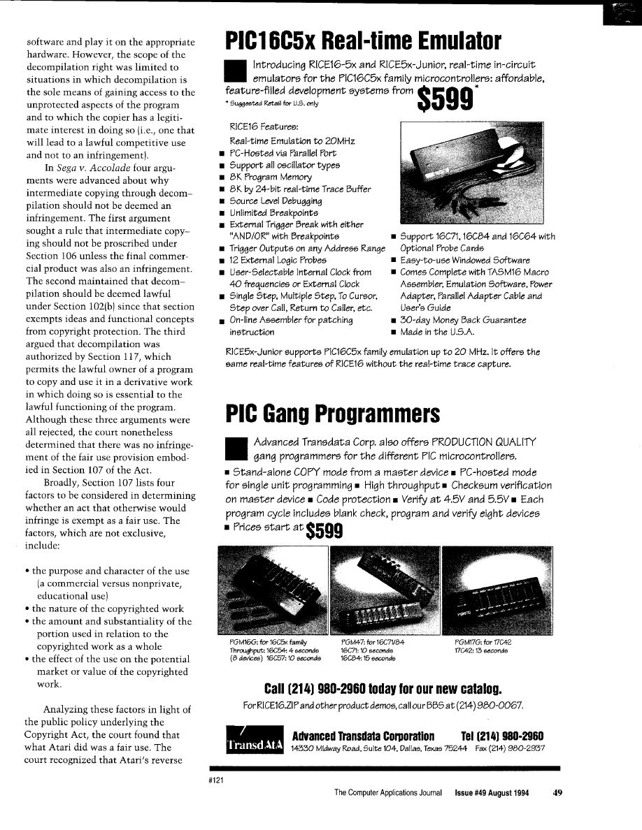
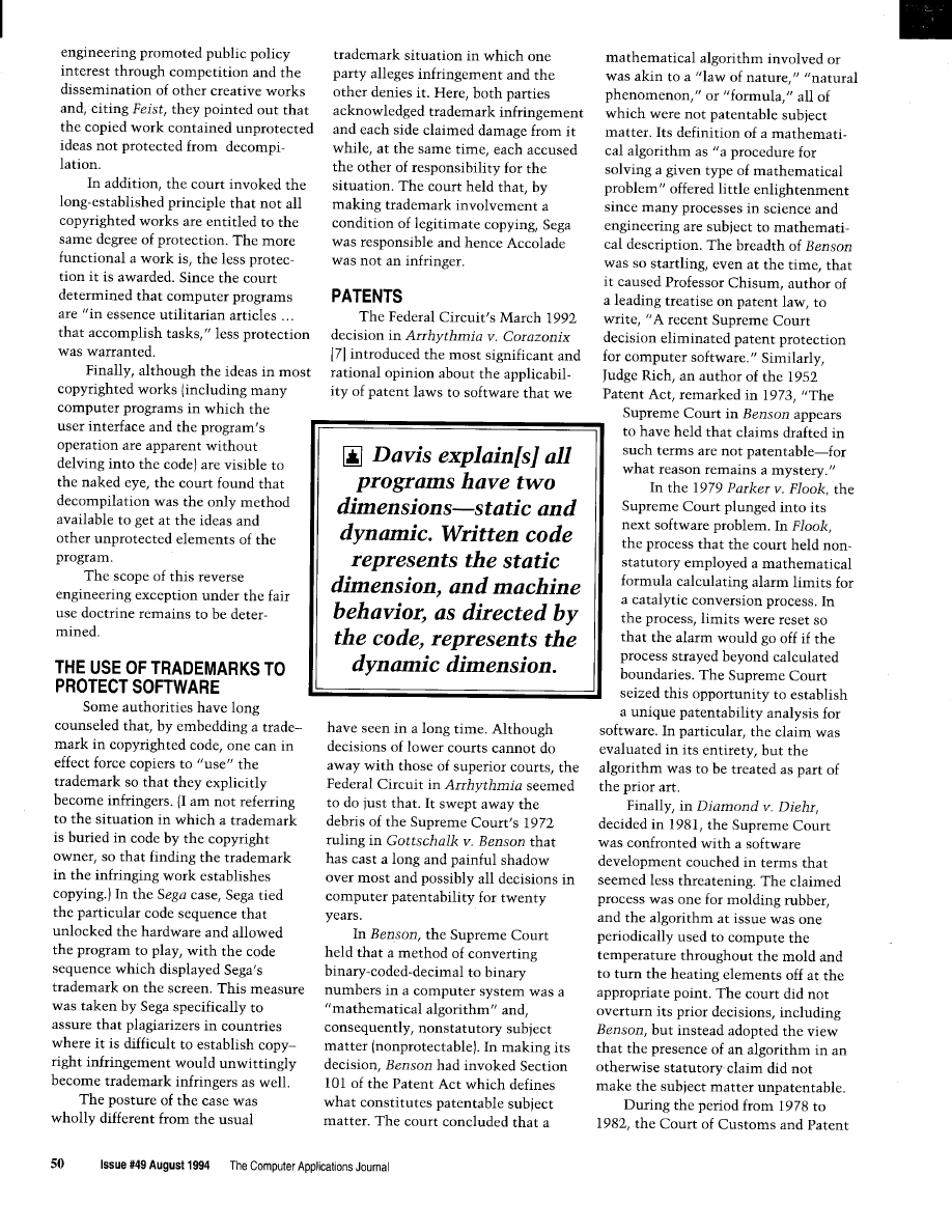
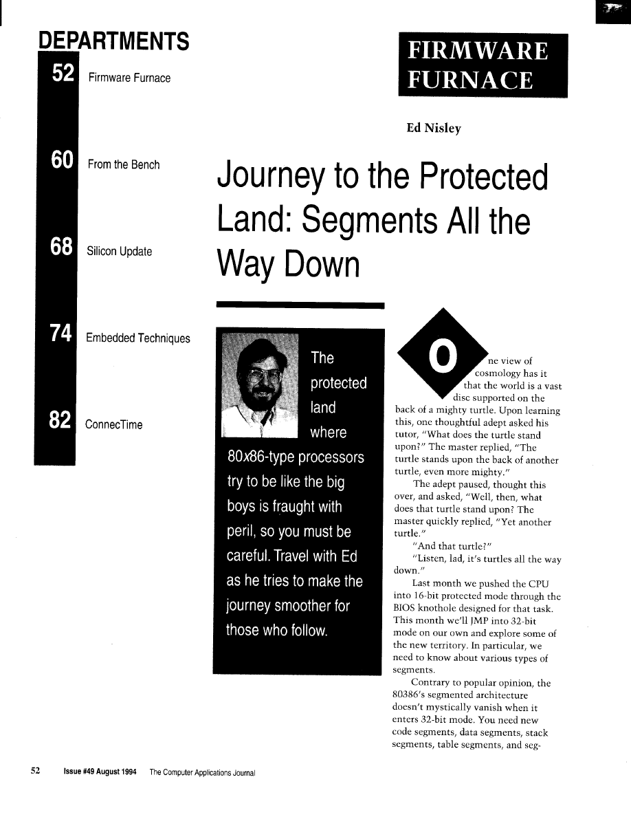
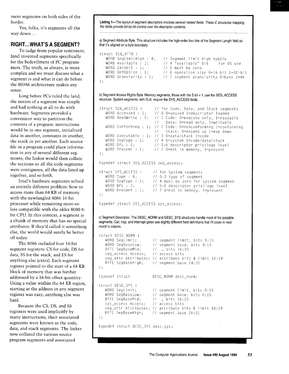
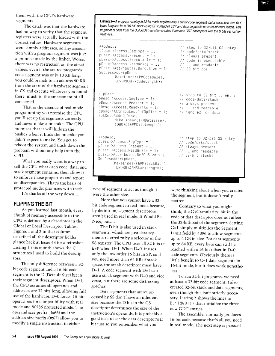
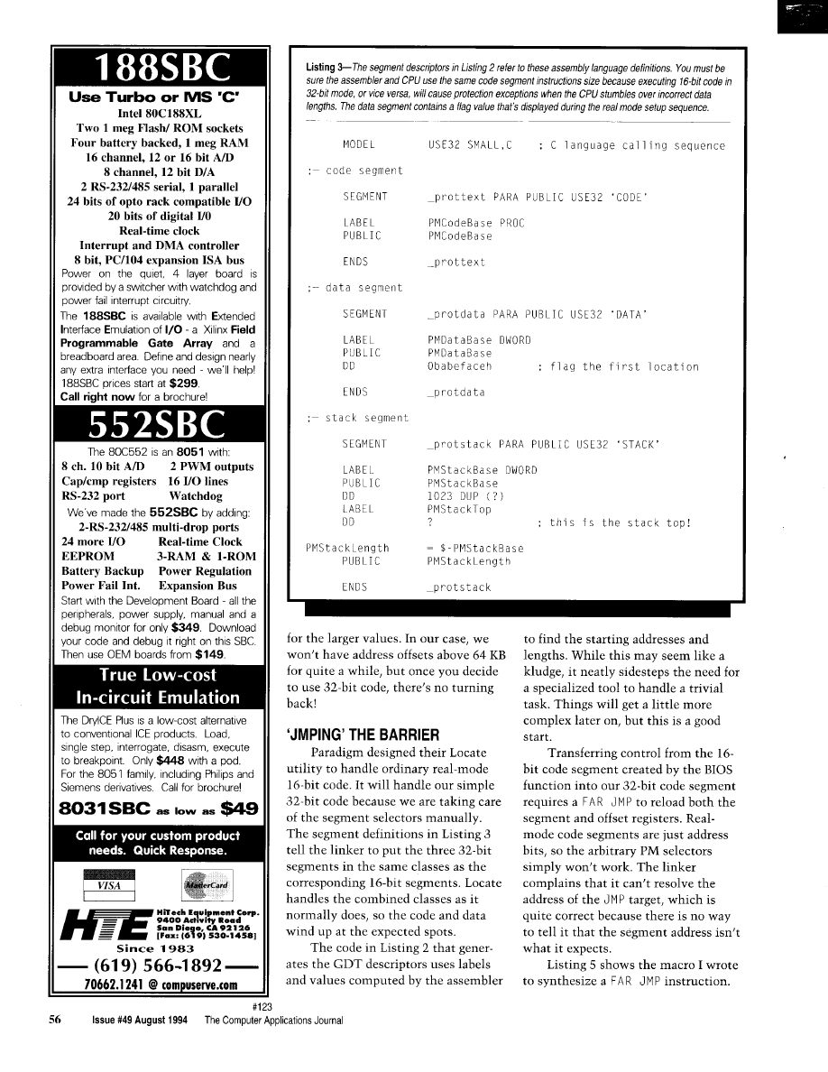
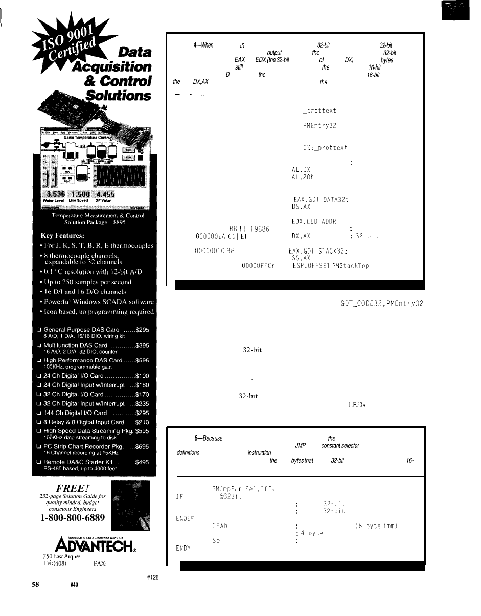
Ave., Sunnyvale, CA 94086
245-6678
(408) 245-8268
Listing
USE32 is effect, the
assembler generates
operands and assumes
addressing. This section of fhe assembler
listing shows code generated af the initial
entry
point Consfanfs loaded info
and
counterparts AX and
require four
each,
while values going info AL use a sing/e byte. The opcodes are same as those in
mode
because the segmenf’s bit specifies operand size. When an instruction requires a
value, such as
OUT
in line 1987, an operand size prefix must precede opcode.
1970 00000000
SEGMENT
1971
1972
PUBLIC
1973 00000000
PROC
PMEntry32
1974
1975
ASSUME
1976
1977 00000000 BA 00000378 MOV EDX,SYNC_ADDR
show entry here
1978 00000005 EC
IN
1979 00000006 OC 20
OR
1980 00000008 EE
OUT DX,AL
1981
1982 00000009 B8 00000048 MOV
set up data seg
1983 OOOOOOOE 8E D8
MOV
1984
1985 00000010 BA 0000031E MOV
1986 00000015
MOV EAX,NOT 6779h
show P3 for '386
1987
OUT
mode
1988
1989
00000050 MOV
set up stack seg
1990 00000021 8E DO
MOV
1991 00000023 BC
MOV
Because it uses a data constant to
generate the selector value, the
assembler doesn’t mark it as relocat-
able and the linker doesn’t try to
relocate it. The macro also inserts the
prefix bytes that specify
oper-
ands and addresses in a 16-bit segment.
Sometimes this high-level assembler
stuff just gets in the way..
After all that buildup, the single
instruction that enters
mode is
anticlimactic:
PMJmpFar
The selector value matches up
with the 32-bit code segment descrip-
tor in the GDT and the offset marks
the first instruction in Listing 4. The
CPU loads the selector, verifies the
segment’s attributes, and fetches the
first instruction shown in Listing 4.
That’s all there is to it.
Once in 32-bit mode, the code
twiddles a few
sets up the SS
and DS registers, and enters a loop that
Listing
the segment values are now arbitrary numbers
real mode assembler and linker
cannot relocate them. This macro synthesizes a FAR
with a
value using data
rather fhan the usual
mnemonics to prevent the assembler from “helping out” with
relocation values. The macro a/so inserts prefix
specify
operands and addresses in
bit segmenfs.
MACRO
0
DB
066h
force
operand size
DB
067h
force
address size
DB
JMP LARGE FAR
DD
OFFSET Offs
offset
DW
Z-byte selector
Issue August 1994
The Computer Applications Journal
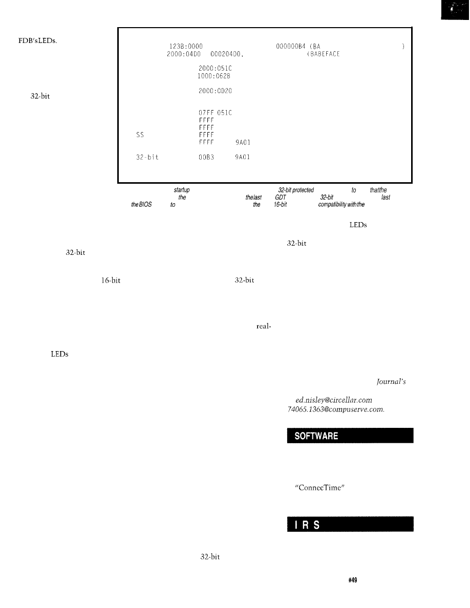
displays a counter on the
A subroutine
converts the count to LED
segments (talk about
function overloading: that’s
the third “segment” we’ve
met so far) to verify that
the
stack is usable
for calls, returns, and
ordinary pushes and pops.
Part of the loop
transfers the FDB’s DIP
switches into the ES
register. All is well if the
switches contain a valid
selector, otherwise the
CPU will cause a protec-
tion exception. This allows
you to exercise the IDT and
demonstrate that your
system really is in pro-
tected mode.
Linked pointers and values from the PM segments...
PM Code
= 00012380, length
78 03 00 00 EC OC 20
PM Data
=
length 00000018
12345678)
PM Stack 2252:0000 = 00022520, length 00001000 (00000000)
Allocating IDT at
Re-vector table
= 0001062B
First IDT entry 062B 0030 8600 0000
Allocating GDT at
GDT NULL
0000 0000 0000 0000
GDT alias
0057 OD20 9202 0000
IDT alias
9202 0000
DS
0000 9202 0000
ES
0000 9202 0000
0000 9202 0000
CS
0000
0000
BIOS CS
0000 0000 0000 0000
code
23B0
0040
d a t a
0017 04D0 9202 0040
s t a c k
OFFF 2520 9202 0040
Figure l--The real
mode
code dumps the first few byfes of each
mode segmenf
verify
linker and
Paradigm’s Locate handled relocation correctly. On/y
three
entries specify
mode because, as in
month’s
code,
“Switch Protected Mode” function requires other
segments for
Original IBM A T’s
80286 CPU.
The IDT is unchanged from last
month, which means the CPU
switches from
mode to 16-bit
mode when it enters the error handler.
Each interrupt gate descriptor in the
IDT specifies the original
PM
code segment descriptor, which
remains ready for use in the CDT.
Although we know nothing can go
wrong (right?), the real-mode code
displays status and tracing information
as shown in Figure
1.
If your system
doesn’t make it to the Protected Land,
check the
and traces to see
where it veered from the trail.
CODE BASE ONE
Although I’m sure you’d like to
see the whole FFTS protected-mode
task switcher presented in the next
column, that’s not the way it’s going
to be. After all, what would I do in
October?
What you will see is a series of
columns exploring the fundamental
building blocks beneath FFTS. For
example, we will explore interrupt
gates by writing an interrupt handler,
activating hardware interrupts, and
measuring the response time. Working
step by step gives me enough room to
explain what is going on without
having to cover everything at once.
Along the way I’ll accumulate a
variety of utility routines that handle
serial I/O, display things on LCD
panels, twiddle the FDB hardware, and
so forth. Most of this code appeared in
C as I built the Firmware Develop-
ment Board; this time around I’ll cast
it in 32-bit assembler to show what it
looks like in PM. You won’t see much
of this code unless PM or
data
makes a big difference in how it’s
handled. For example, accessing the
real physical memory of the graphic
LCD panel is a little trickier now.
In two or three months, the
mode code will atrophy to a loader
that doesn’t display quite so much
diagnostic information. The PM code,
by then a disk file of its own, will split
into several distinct modules. Until
then, the code will remain a simple
monolithic chunk to reduce the
number of files and keep our attention
focused.
What you should do is participate:
download the code, experiment with
it, and report back on the BBS. First of
all, if it doesn’t play, I want to know!
More important, you should modify
the code to make sure you understand
how the machinery works. Try
different interrupts, tweak the timings,
add bells and whistles. After all, it’s
small enough that you can’t go too far
wrong and safe enough that you won’t
get hurt!
RELEASE NOTES
The BBS code this month puts
your CPU into
protected mode,
setting a variety of
along with a
way to track any problems. Once in
mode, it blinks an LED on the
printer port and shows an
incrementing count on the FDB LED
display. The real-mode code sets up
the GDT entries and sends a variety of
information on the memory addresses
going into each descriptor to the serial
port before entering PM.
Next month, I’ll examine inter-
rupt and error handlers in the IDT and
make a few timing measurements.
q
Ed Nisley, as Nisley Micro Engineer-
ing, makes small computers do
amazing things. He’s also a member of
the Computer Applications
engineering staff. You may reach him
at
or
Software for this article is avail-
able from the Circuit Cellar BBS
and on Software On Disk for this
issue. Please see the end of
in this issue for
downloading and ordering
information.
413 Very Useful
414 Moderately Useful
415 Not Useful
The Computer Applications Journal
Issue
August 1994
59
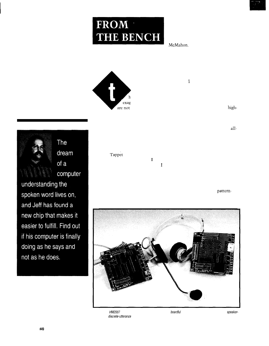
Ta( I) king
Control
Jeff Bachiochi
he death of radio
has been greatly
exaggerated. If you
are not a connoisseur of
(hard or soft) rock, jazz, C&W, rap,
pop, hip-hop, swing, or classical music,
then one of the public or college
stations surely carries programming to
please. Talk shows enjoy peak ratings
these days. With a twist of the dial you
can be enlightened and entertained by
programming like “Car Talk” with
hosts the
Brothers.
When driving any distance, like
to listen to prerecorded audio dramas
have on cassette. Something about
letting your mind paint its own
pictures helps to solidify the space
between fantasy and reality. Audio is a
powerful medium unto itself.
Even television has its audio
memories. Some personalities have
become synonymous with a particular
program from just one single phrase.
“Herrrzzz Johnny” is the best example
that comes to mind. We can’t envision
the “Tonight Show” without Ed
Although in video a picture
is worth a thousand words, in audio a
couple of well-chosen words can paint
an entire picture. Or those same
words
can take control of the picture.
TAKING CONTROL
When think of voice recognition
today, PCs with ungodly amounts of
memory come to mind. Memory for
mammoth prerecorded vocabularies
needed as baseline comparisons to
real-time audio. Memory for the
speed processing necessary to analyze
the live input and attempt to match it
with one already in existence.
Today, attempts to create the
powerful recognition algorithm are
cloaked in secrecy, yet great advances
have been made in voice recognition.
Phrase recognition has finally reach
the usable stage, while continuous
recognition, in all honesty, still has a
ways to go. So, for the near future,
voice recognition will remain a slave
of memory and speed.
Some silicon has been developed
which combines a number of masked
preselected phrases with a
matching algorithm. Refer to Michael
Swartzendruber’s “Control Your
Photo l-The
does on a sing/e chip
what required a
of electronics just a few
years ago:
dependent,
voice recognition.
60
Issue August
1994
The Computer Applications Journal
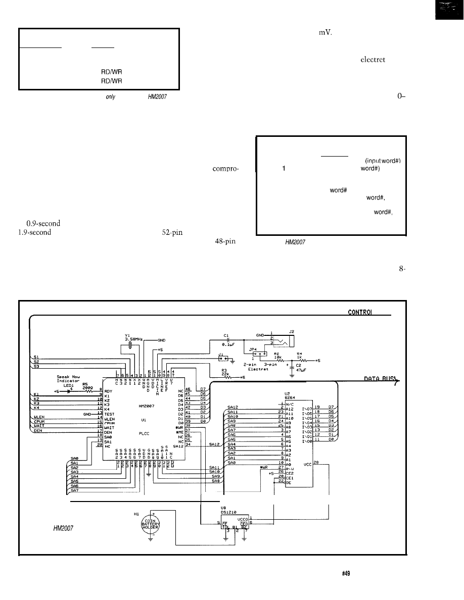
Status Register
Value (K-Bus)
Meaning
2
Ready for a command from the CPU
1
Ready for audio input
3
Ready to
lower nybble
0
Ready to
upper nybble
aggravating to have to go
is about 20
I’ve found a bit of
though a third party to get
preamplification may be required
answers to the more
(depends on microphone used) to avoid
technical questions I had
having to shout into the
mic.
about the device and its
usage. Not having an
MANUAL MODE
applications engineer
In manual mode, seven I/O lines
create a twelve-key scanned matrix:
9, clear, and train. Twenty additional
I/O lines create the twelve address and
is received by other developers.
eight data connections supporting the
There must have been
Table
l-Besides
being busy, there are
four states the
can
available in the United
be in.
States will definitely have
an affect on how this chip
Telescope by Voice” in issue 32
(March 1993). Although limited to
eight unchangeable phrases, the
hardware is simple. Why can’t some-
one take this a step further and allow
the vocabulary to be user selected.
Well, they can, and they have.
HMC (Hualon Microelectronics
Corp.) distributes the HM2007 voice
recognition chip through the Summa
Group. The HM2007 will store up to
40
durations or up to 20
durations of audio. Succes-
sive audio is sampled and a “best
guess” is provided for the closest
match.
some heavy disagreements
during the development of
Command Value
Meaning
this device. The final design
(K-Bus)
(parameter)
0
Clear a trained word
seems to be a weak
Train a word (input
mise between a manual and
CPU-controlled device. This
makes it more difficult to use
effectively in either mode.
2
Recognize a word (audio in)
3
Give recognition result
(get
and Score)
4
Upload a word (input
get
length and stored patterns)
The handiest package
5
Download a word (input
available
for the HM2007 is
length, and saved patterns)
6
the
PLCC, although it
Reset (clears all words)
is also available in a
Table
2-The
supports seven CPU-issued commands.
PDIP and a 48-pin die. It
contains an analog AGC front end,
SRAM and a display register. External
Information other than that
A/D converter, and masked CPU
SRAM is used for phrase storage. An
contained in the device’s data sheet is
running at a handy 3.58 MHz. The
bit display register holds two BCD
difficult to come by. I found it a bit
minimum audio signal input necessary
digits. These digits provide the user
BUS
Figure
l-The base circuitry needed to
support the
includes just a
battery-backed RAM, a crystal, and a
mic input.
The Computer Applications Journal
Issue
August 1994
61
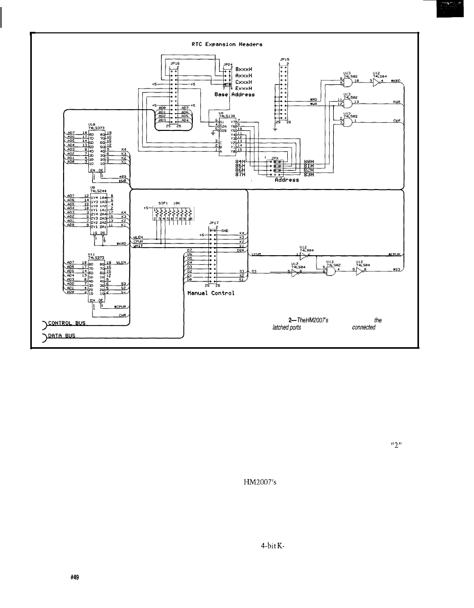
O f f s e t
Header
Figure
CPU
mode requires use of
since the chip can’t be
right to the
processor
bus.
visual
feedback about the state of the
HM2007.
Using the keypad, any word can be
cleared, trained, or recognized. During
training, two types of errors may be
encountered. If the sound duration is
either too short or too long, it is
flagged by the system and displayed as
BCD digits 55 or 66, respectively. The
user must then retrain that word.
Once training is complete, recognition
mode is entered and successive sounds
are compared to the trained patterns
for a match. There is an internal value
[a summation of differences in pattern
a CPU, the manual mode does not
offer any indicator of the confidence
level for the recognition process. With
manual mode, you are limited to the
internal confidence setting to deter-
mine whether or not a match has been
made.
CPU MODE
The CPU mode reconfigures the
keypad’s seven I/O lines as a bidirec-
tional nybble bus [K-bus) and three
control lines (S-bus). The first control
line chooses between the
status register and data register. The
Besides being busy, there are only
four states the HM2007 can be in.
These are reflected in the status
register as the values 0, 1, 2, or 3 as
shown in Table
1.
CPU commands instruct the
HM2007 to perform a specific func-
tion. There are seven such commands
as shown in Table 2. [Upon power-up,
the HM2007 presents a status
and
awaits a command.)
The HM2007 was not designed to
be directly interfaced as an I/O device.
Because of this, it requires a bidirec-
tional &bit-programmable port or two
matching) that must not be exceeded if
second and third control lines are read
nybble output registers and one nybble
the device is to indicate a match and
and write enables. Pulling the RD line
input register. I chose to use the latter
display the matching word number. If
high forces the HM2007 to place either
so the circuit could be used with the
this value is exceeded, then a 77 is
the status or data register’s 4 bits on
RTC stacking series of controllers.
displayed indicating no match.
the K-bus. Pulling the WR line high
Adding another peripheral to the
Although the display register (two
forces the HM2007 to read the
existing RTC line only strengthens its
BCD nybbles) could be interrogated by
bus.
effectiveness and versatility.
62
Issue
August 1994
The Computer Applications Journal
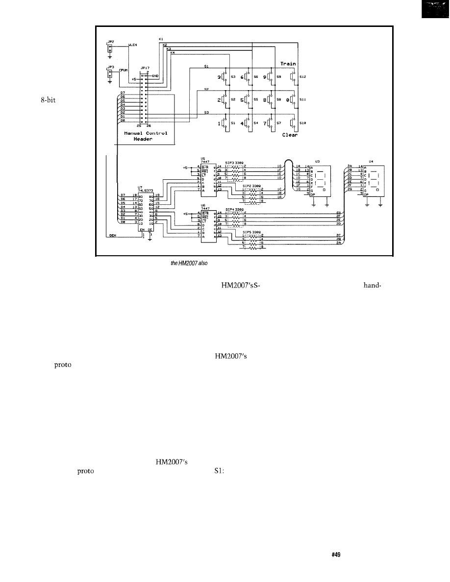
frequency data are
extracted from the
audio. Sampling is
done for either 0.9 or
r
1.92 seconds, depend-
ing on the logic level
presented to the
S c a n n e d
Keypad
BCD Display
Figure 3-/n addition to CPU mode,
supports a manual mode using push buttons and LED displays.
Refer to Figure 1
for the base circuitry
needed to use the
HM2007. Audio from
an external micro-
phone is processed
through an internal
AGC and fed into the
internal
A/D
converter. Both
amplitude and
WLEN input. The
sampling length also
determines the
maximum number of
words in the vocabu-
lary (40 or 20, respec-
tively). Note that this
is a maximum and not
a requirement.
Vocabularies which
are smaller in size
have higher (correct) rates of recogni-
outputs which share the
tion.
and K-bus I/O lines with the keypad.
The vocabularies are held in
SRAM. By battery backing the SRAM
and holding the WAIT input at logic
low during power-up, the vocabulary’s
data patterns can be preserved while
the system is off. I placed the CPU
interface circuitry shown in Figure 2
on the same
board with the
HM2007. I could have used port
1
of
the 8052 as the interface, but I wanted
to make the HM2007 look like an I/O
device so it could be used with the
other RTC processor boards. I also
chose to use discrete registers for
clarity as opposed to an 8255, 6821, or
other multiregis-tered part.
HM2007 SEMAPHORE
The CPU mode’s K-bus user
output register is only enabled when
the S3 control line (WR) is pulled to a
logic high by the S-bus user output
register. A high on the
S3
input indicates that the user has
placed information on the K-bus and
the information can now be read by
the chip. The HM2007 receives both
commands and data using the above
procedure.
By wiring up a header with all the
signals necessary to use the HM2007
in manual mode, I built a second (and
optional) piggyback
board to hold
the keypad and display. This can be
used as an alternate method of training
and testing. When the CPU input is
pulled to a logic low (by the jumper on
this board), the HM2007 is placed into
manual mode. In this mode, external
circuitry disables the I/O register
Likewise, while a logic high is
placed on the S2 input (RD), the
HM2007 will output information on
the K-bus. The user determines
whether the information comes from
the
status register or data
register by the state of
logic low for
status and logic high for data.
Since the HM2007 is interfaced
through I/O ports as opposed to the
CPU bus, the user must constantly
poll the status register to determine
what state the HM2007 is in. The
command sequences, therefore,
contain intertwined software
shaking.
EXERCISING THE HARDWARE
Writing a BASIC subroutine for
each command was easy (see Listing 1)
using the flowcharts in the data sheet
as a guide. All seemed like a piece of
cake until I ran into problems getting
back the word number and score from
the HM2007. When WLEN was high
(which puts the HM2007 into the
higher 40 word, but shorter 0.9 second/
per word mode), the chip refused to
present the score. The program would
just hang. Since there is no reset on
the HM2007, things got locked up
tighter than Fort Knox.
After considerable frustration with
checking and rechecking my wiring,
flowcharts, and coding, I broke down
and called for assistance. I talked with
Louis Gerhardy of the Summa Group.
“Louis. I would like to report a
few errors I’ve found in the data sheets
you faxed me,” I offered as if a carrot
on a stick.
“Sure, what ya got?” the enthusi-
astic voice replied.
The Computer Applications Journal
Issue
August 1994
6 3
“I’m guessing the status check on
flowchart 2 should be a value 1 instead
of 2 and the command in flowchart 7
should be
“Yes, yes that is correct,” came
the acknowledgment.
“Well, if there are errors in these
two charts, is it possible there is a
problem with chart
I asked
gingerly. A short pause stretched into a
long one.
Finally, after what sounded like a
bunch of paper shuffling, “I do have a
note scratched in the border here. Bug
in result command when..
looks like WLEN, yes, WLEN is high.
Work around is drop WLEN to logic
low when in result command. Does
that make any sense!”
“You’re
asking me!” I
thought to
myself, then answered, “No, but let
me think about it. Thanks.” Louis
must be as frustrated as I; he handles
this device and is not an applications
engineer.
Back in the code, I altered the
result routine to twiddle WLEN low
while asking for the data (a no-no
according to the data sheet). As if by
magic the command now returned the
proper response. Gotcha. Grrr.
Once I had words trained, I needed
a way to offload them so I wouldn’t
have to retrain them if the memory
backup failed. I use ProComm on my
PC to give me a smart terminal
interface for the RTC52. By using the
line pacing protocol, program uploads
to the processor are paused after each
line (carriage return/linefeed) to allow
the RTC52 to process the line and
catch up. When ready, the RTC52
automatically returns the
charac-
ter. ProComm resumes sending the
next line after receiving that character.
Serial uploading from the PC
using BASIC’s GET or I N PUT com-
mands is usually not successful.
BASIC is slow compared to the rapid
rate of a serial transmission, so
characters always get lost. Lost, unless
handled like the line pacing of a
program upload. This means one
character at a time.. .or one string.
The word data coming from the
HM2007 is in
blocks, so why
not put those eight nybbles in a string
and move it that way! One other
Listing
in the
makes writing
code much
easier. However,
for
10 STRING
20 BASE=OEOOOH
30
40
50
60
70 PRINT "Press 0 for 20 words 1.92
or 1 for 40 words
0.9
80 G=GET : IF
THEN GOT0 80
90 IF
THEN
70
110
170
180
190
195
200
210
220
230
240
250
260
270
280
290
300
310
320
330
340
345
350
360
370
380
390
400
410
420
430
440
450
460
470
480
IF
THEN
ELSE WL=O
REM STATUS
FOR VOICE INPUT
REM STATUS
FOR COMMAND A COMMAND
REM STATUS
FOR WLSN OR AVAILABLE
REM STATUS O=READY FOR MSN OR AVAILABLE
PRINT "Speech Recognition Demo using the HM2007"
PRINT "Checking HM2007 status"
:
1000
PRINT Press Menu Selection"
PRINT "1 Train a Word"
PRINT "2 Recognize a Word"
PRINT "3 Save a Vocab"
PRINT "4 Load a Vocab"
PRINT "5 Turn
IF
THEN PRINT "on ELSE PRINT
PRINT "status reporting"
PRINT "6 Clear all memory"
PRINT "7 End"
G=GET
IF
THEN 380
IF
THEN 380
IF
THEN GOT0 3000
IF
THEN
4000
IF
THEN GOT0 6000
IF
THEN GOT0 7000
IF
THEN
IF
THEN GOT0 2000
IF
THEN STOP
230
1000 REM status check
1010
1020 IF
THEN RETURN
1030 IF
THEN GOT0 1000
1040
PRINT "Checking Status
1050 IF
THEN PRINT Ready for Audio Input"
1060 IF
THEN PRINT Ready for Command"
1070 IF
THEN PRINT LSB Ready"
1080 IF
THEN PRINT MSB Ready"
1090
360
2000 REM CLEAR ALL MEMORY
2010
2020
1000
2030
2040
2050
1000
2060
230
3000 REM TRAIN
3010
3020
1000
3030 PRINT
3040 PRINT "Enter the
INPUT N
3050 IF
3060 PRINT "Type in a
INPUT
3070 LSNN=N.AND.OFH
3080
3090
XBY
word number to train
THEN GOT0 3030
description of the audio for word
(continued)
64
Issue August 1994
The Computer Applications Journal
Listing
l-continued
3 1 0 0
3110
3120
1000
3130
3140
3150
316C
3170
3180
3190
3200
3210
3220
3230
3240
4000
4010
4020
4030
4040
4050
4060
4070
4080
4090
4100
4110
5000
5010
5020
5030
5040
5050
5060
5070
5080
5090
5100
5110
5120
5130
5140
5150
5160
5170
5180
5190
5200
5210
5220
5230
5240
6000
6010
6020
1 0 0 0
6030
6040
GOT0
6050
6060
6070
6080
6090
6100
6110
6120
6130
6140
6150
6160
6170
6180
6190
6200
6210
1 0 0 0
PRINT "Please Speak Now..."
5000
IF
THEN PRINT "Try Again"
GOT0 3070
GOT0 230
REM RECOGNIZE
1 0 0 0
1 0 0 0
PRINT "Please Speak Now..."
IF
THEN 4080
5000
IF
THEN PRINT "Try Again"
GOT0 4000
GOT0 230
REM RESULT
1 0 0 0
PRINT "Looking for LSN"
1 0 0 0
PRINT "Looking for MSN"
1 0 0 0
P = P - 1
IF
THEN R=V GOT0 5070
1 0 0 0
PHO. "The word recognized was
PRINT "The score was
RETURN
REM UPLOADING
PRINT "Enter the word number to save
N
IF
THEN GOT0 6020
IF
THEN PRINT "Word
NOT
6000
PRINT "Press any key when ready to accept data"
G=GET IF
THEN GOT0 6060
1000
:
:
:
1000
:
:
:
:
1000
:
:
:
:
1000
rained"
NEW
Data
Acquisition
Catalog
Covers expanded
low cost line.
1994 120 page catalog for PC, VME,
and Qbus data acquisition. Plus infor-
mative application notes regarding
anti-alias filtering, signal condition-
ing, and more.
NEW Software:
and more
NEW Low Cost Boards
NEW Industrial PCs
NEW Isolated Analog and
Digital Industrial
New from the inventors of
plug-in data acquisition.
Call, fax, or mail for your
free copy today.
ADAC
American Data Acquisition Corporation
70 Tower Office Park, Woburn, MA 01801
Phone: (800) 648-6589 Fax: (617) 938-6553
The Computer Applications Journal
Issue August 1994
65
Replace Four
Conventional PC/l 04
Modules with
One
CMF8680
mbedded PC/XT Controller
Power Manaaement
PC/XT compatibility with 286 emulation
14 MHz,
C&T
CPU
I
only;
at 14.3 MHz, 1 W at 7.2 MHz
Intelligent sleep modes, 0.1 W
in Suspend
ROM-DOS and RTD enhanced BIOS
Compatible with MS-DOS real-time
operating systems
I
bootable solid state disk free software
configuration EEPROM (2K for user)
on-board DRAM
IDE floppy interfaces
I CGA CRT/LCD controller
I Two RS-232 ports, one RS-485 port
Parallel, XT keyboard speaker ports
I Optional X-Y keypad scanning/PCMCIA
interface
Watchdog timer real-time clock
Expand This Or Any PC/l 04 System
with the
CM106 Super VGA
Controller
Mono/color STN TFT flat panel support
Simultaneous CRT LCD operation
I Resolution to 1024 x 768 pixels
Displays up to 256 colors
Product Development with the
SK-CM1 06-X Starter Kit
kit includes the CMF8680
CM106 SVGA controller,
02 keypad
scanning/PCMCIA
CMF8680
cable kit VGA monitor cable for just
$1295.
compliant modules
I
CM104 1.8” hard drive carrier
I
analog I/O modules
I
4-20
analog output modules
I opto-22 digital I/O modules
For more information on our
and
ISA bus products, call today.
Real Time
Devices USA
200 Innovation Blvd.
l
P.O. Box 906
State College, PA 16804 USA
234-8087 Fax: (814) 234-5218
Europa
l
RTD Scandinavia
Time
is a founder of the
Listing
l-continued
622C
623C
624C
6250
6260
6270
6280
6290
6300
6310
6320
6330
6340
6350
6360
6370
6380
6390
6400
6410
6420
6430
6440
6450
6460
6470
6480
6490
6500
6510
6520
6530
6540
6550
6560
6570
6580
6590
6600
6610
6620
6630
6640
6650
6660
6670
6680
6690
6700
6710
6720
6730
6740
6750
7000
7010
7020
7030
7040
7050
7060
7070
7080
7090
GOT0
7100
7110
7120
7130
7140
7150
7160
7170
7180
1 0 0 0
IF
THEN
1 0 0 0
:
1 0 0 0
1 0 0 0
1 0 0 0
1 0 0 0
1 0 0 0
1 0 0 0
1 0 0 0
IF
THEN GOT0 6320
PRINT "-END"
GOT0 230
REM DOWNLOADING
PRINT "Ready to accept data"
INPUT
P=l
IF
THEN PRINT "File Error"
GOT0 230
IF
THEN
GOT0 7050
IF
THEN GOT0 7100
IF
THEN GOT0 7100
IF
THEN GOT0 7100 ELSE PRINT
230
IF
THEN
IF
THEN PRINT "Word ii invalid"
GOT0 230
PRINT "Now downloading word number
of length
1000
(continued)
66
issue August
1994
The Computer Applications Journal
Listing l-continued
7190
7200
7210
7220
7230
7240
7250
7260
7270
7280
7290
7300
7310
7320
7330
7340
7350
7360
7370
7380
7390
7400
7410
7420
7430
7440
7450
7460
7470
7480
7490
7500
7510
7520
7530
7540
7550
7560
7570
7580
7590
7600
7610
8000
8010
8020
8030
8040
8050
8060
8070
8080
8090
1 0 0 0
XBY
1 0 0 0
X B Y
1 0 0 0
: XBY
1 0 0 0
:
: XBY
IF L=O THEN
INPUT
:
:
1000
:
:
:
1000
:
:
1 0 0 0
1 0 0 0
1 0 0 0
:
:
:
1000
:
:
:
1000
:
:
:
1000
:
:
IF
THEN GOT0 7320
8000H (NOT NECESSARY)
GOT0 7030
REM
SAVES PROGRAM INTO NVRAM A
FOR
TO
NEXT X
thought about the data is appropriate
here: since it is in nybbles (O-15), why
not add 20h to each value to make
them printable characters? This avoids
control-character unpleasantries.
easy handling using any ASCII editor.
This also lets you prepare separate files
of differing vocabularies.
SPEAKING OF APPLICATIONS
Now that we know how the data
Picture this: Saturday afternoon.
must be formatted to
properly
The playoffs are on and you’ve got
into the
and the HM2007, the
multiple teams to keep track of. A cold
download portion is just a matter of
beer in one hand and a hoagie in the
collecting the data and outputting it in
other. You speak, “TV..
.O..
the compatible format. Each word’s
2.” The channel changes and you’re
data is output separately and collected
there as a
is sunk. You decide
by
into separate
files.
to tape the other channel so you won’t
You can concatenate any of these
miss a moment of these last four
words
files) into a single file for
minutes. You speak again, “VCR..
record.” As the front panel indicates
life, you think you hear something.
Once more you speak, “TV..
Ring, ring, it’s the phone, but it’s
answered almost immediately by one
of the kids. You don’t get phone calls
anymore; remember, you just live
here. “TV..
you repeat again.
Instantly, you’re back in the action.
This application uses the RTC52
and the MCIR-Link in an interactive
RS-232 mode. The MCIR accepts
[where x is a number) as a
command to send out a prerecorded IR
transmission. All the television and
VCR functions were trained on the
MCIR, and when a spoken word is
recognized, the RTC52 outputs the
appropriate
command to the
MCIR-Link. A null-modem cable is
needed here because both the RTC52
and the MCIR-Link look like DCE
devices.
I admit this is not all that practi-
cal, but I bet you can come up with a
situation where it does make sense. Or
maybe like me, you just want to have
a little fun.
P.S. HMC, if you’re listening, I
think the hardware implementation
and documentation could be improved,
just a bit. But you’ve probably already
(‘scuze me] recognized that!
q
Special thanks to Louis Gerhardy
(The Summa Group Limited) and H.C.
Lee (Hualon Microelectronics Corp.).
Bachiochi (pronounced
AH-key”)
is
an electrical engineer on
the Computer Applications
engineering
staff.
His background
includes product design and manufac-
turing. He may be reached at
The Summa Group Limited
1 California St., Ste. 1940
San Francisco, CA 94111
(415) 2880390
Fax: (415) 288-0399
416
Very Useful
417 Moderately Useful
418 Not Useful
The Computer Applications Journal
67
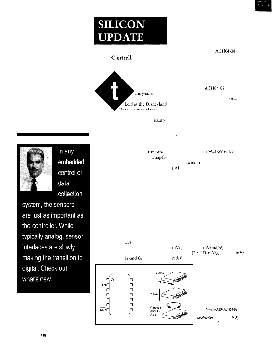
“G” WHIZ
Don’t expect the digital takeover
to happen overnight. The first tenta-
tive steps will include chips that
combine analog and digital interfaces
to ease the way for wary designers.
Consider the AMP
accelerometer ($40 qty. 1). The device
integrates piezoelectric sensors
configured to measure acceleration in
three axes: Y, Z, and rotation around Z
as shown in Figure 1.
While piezo accelerometers are
nothing new, the
is
innovative because of its integrated
interface logic that culminates
hooray-a digital output mode.
As shown in Figure 2, the three
raw inputs are fed to amplifiers with
programmable gain which, in turn,
feed comparators with programmable
threshold. The result is a digital Q (or
Q
output flagging a “shock” defined
by the user-specified gain, threshold,
and reference voltage: 3-53 g’s for the
Y- and Z-axis and
rotation about Z. As shown in Figure
3, once
from low-power (200
o r
amplified
In the
Realm of
the Sensors
Tom
“Sensors Expo” was
Hotel-a nice place if
you don’t mind pictures of Mickey
Mouse and Goofy instead of the
by-the-numbers masterpieces that
grace the typical tourist trap.
However, except for the few who
qualify as an electronic Michelangelo,
a paint-by-the-numbers design mental-
ity is the way to go lest your
market be measured in Sistine
like terms.
It’s an oft-repeated theme of
“Silicon Update” that much of the art,
albeit black, of scientific and industrial
applications revolves around sensor
interfacing and analog design antics.
Sure, you can attribute some of
my “analogphobia” to a simple case of
bit-head bias. Nevertheless, even an
objective observer must admit that the
process control world is way behind
the digital eight ball.
The inertia to do things the “good
old way” is strong, but under constant
attack by wave after wave of ever more
powerful digital
Though reluctant,
the data acquisition and process
control folks are slowly, but surely,
moving into the
age.
V D D
ROUT
VREF
N/C
NIC
OUT
RST
PROGV
DATA
CLK
SELECT
GND
Figure
accelerometer measures
in three axes: and
rotation around
68
issue
August 1994
The Computer Applications Journal
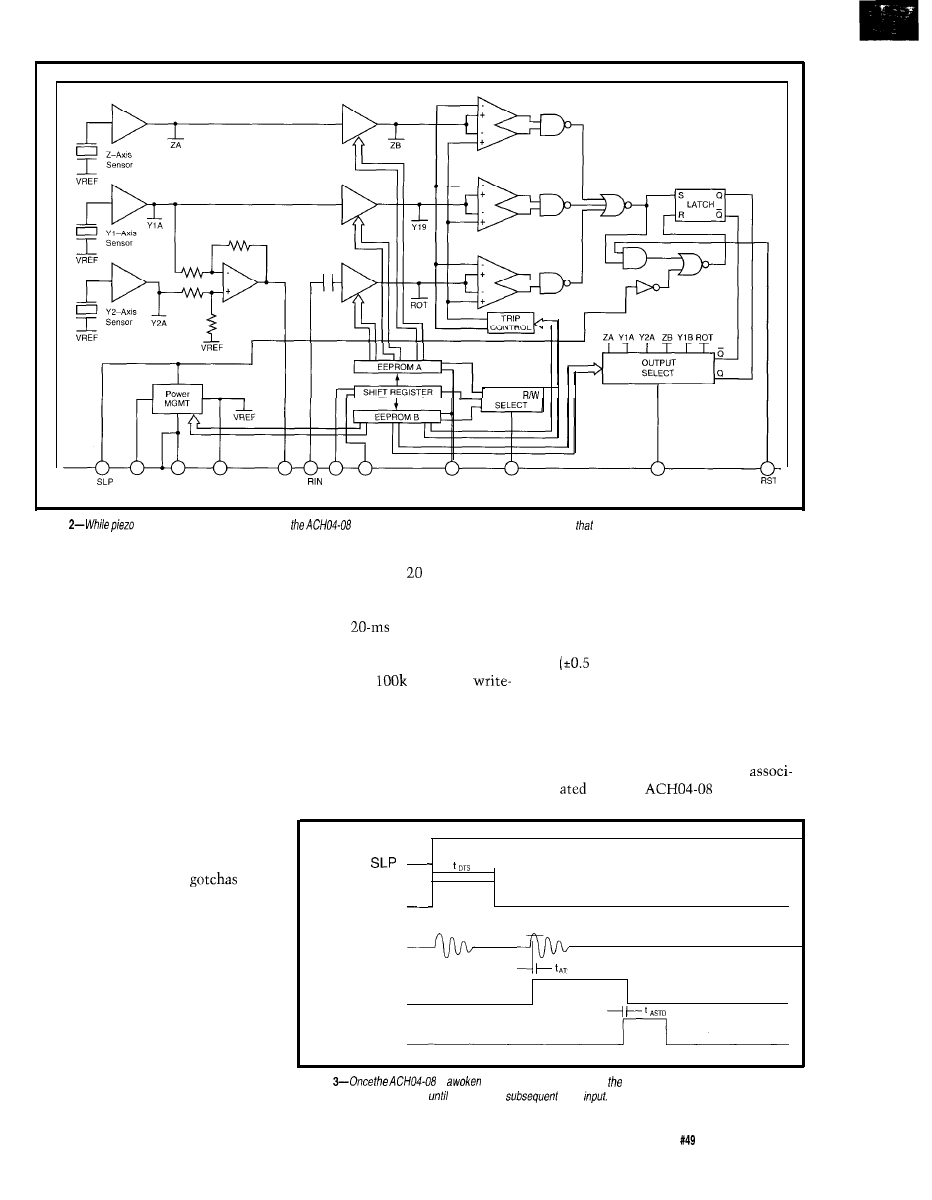
CONDUCTIVE HOUSING CONNECTED TO GRD
EEPROM
VDD
GND
VREF
R O U T
CLK DATA
PROGV
SELECT
OUT
Figure
accelerometers are
nothing new,
is innovative because of ifs integrated interface logic
produces digital outputs.
The idea of offering both digital
and analog outputs is fine, but I
question funneling both through the
same pin (though note that the
rotation output-ROUT-is separately
available). For instance, if two pins
were provided, it would be possible to
connect the digital output to a micro’s
interrupt request and the analog out to
an A/D converter. Then, the micro
could ignore minor jiggles, yet still
take detailed readings via the ADC in
response to a shock interrupt.
reading, missing the first, and likely
most interesting, ms while making
the mode switch would seem problem-
atic for high-speed applications.
At first glance, it seems fairly easy
to duplicate two-pin functionality by
dynamically reprogramming the
OUTPUT SELECT bits and adding a
gate or two to route the single output
pin. However, beware of
when
contemplating such a scheme.
design that did nothing but switch
back and forth continuously could die
The
reprogramming time
in less than an hour! Yet, a more
that might be “too slow” in an
application sense may be “too fast” in
terms of the
EEPROM
careful design, perhaps coupled with a
cycle endurance limit. A worst-case
little reality-checking software, can
but be careful not to simply assume (as
or digital (but not both) fashion, it
in ASS-of-U-and-ME) it away.
obviate the write endurance concern,
If you still want to reprogram in
situ,
start digging around in your
might still be wise to arrange for
system for a rather unlikely -16-V
reprogramming. I think there is a big,
V, thank you) PROGV voltage.
Even if you choose to simply use
yet largely overlooked, gotcha
the chip in the clearly intended analog
with the
and other
Clocking the data into the on-chip
shift register via the CLK and DATA
lines takes only a dozen or so micro-
seconds, but the minimum program-
ming time (i.e., subsequent pulse on
the PROGV pin) is on the order of 10
ms each for EEPROM A (gain) and
EEPROM B (VREF, TRIP, and OUT-
PUT SELECT). Assuming the idea is to
interrupt with the digital output and
then quickly sample the analog
INT. INHIBIT
Trip Level
SHOCK INPUT
DIGITAL OUT
R S T
Figure
is
from low-power sleep mode, output is asserted when a shock is
defected and remains latched
c/eared by a
reset
The Computer Applications Journal
Issue
August 1994
69
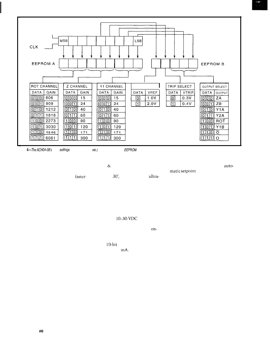
DATA
SHIFT REGISTER
VREF SELECT
Figure
user
(gain,
threshold,
are he/d in 14 bifs of
EEPROM-based chips: data retention
time.
Yes, ten years is a long time in the
electronics business and, in the
paced sectors, it’s marginally valid to
ASS-U-ME that your gizmo will have
long since become a door stop or boat
anchor. On the other hand, industrial
applications tend to be much more
long-lived, and examples abound of
machines that outlast their masters.
So, should you decide to ignore
the data retention issue, I suggest you
mark your calendar. It might be wise
to be on vacation or otherwise be “out
of the office” 10 years from now when
the phone starts ringing.
SONIC TONIC
First-generation ultrasonic
transducers were little more than
speaker-microphone combinations,
leaving the burden of driver modula-
tion, echo detection, and other
housekeeping chores to the system
designer. Now, reflecting the “smarter
is better” trend, transducers are
starting to integrate the various bits
and pieces-amps, filters, power
supply, and so on-needed for a total
solution.
harsh-environment-tolerant steel and
Consider the EDP (Electronic
polymer package.
Design Packaging) Sonaswitch 1750
(Photo 1) which measures distances
from I” to
as is typical for
sonic rangers.
What isn’t typical is the amount
of glue logic integrated in the 1.5” x 6”
First is a built-in high-efficiency
switching power supply that operates
from a wide
(0.5 A max)
input range. Though they haven’t gone
as far as offering digital output,
board amplification and conditioning
does allow them to offer eminently
usable
analog outputs-both O-5
VDC and 4-20
Ah, if only all
analog gadgets would so easily mate
with micros.
heavy-duty steel gadgets. On the other
inputs and NPN outputs that support
hand, it does include DOS upload,
download, calibrate, and monitor
calibration (zero/span) and an
software.
monitoring scheme
with programmable hysteresis and
glitch reduction.
At $450 in singles, the 1750 isn’t
cheap, but that’s usually the case for
Having accepted the burden of
providing meaningful outputs, the
1750 goes for the gusto with built-in
temperature calibration, program-
mable slope (i.e., the polarity of the
output can be inverted), and adjustable
output filter, easing your micro’s
processing burden considerably. The
settings are programmed via built-in
RS-232 port.
Other goodies include push-button
Besides, if you’re in a hurry and
aren’t making a zillion gizmos, the
price is really quite reasonable. Figure
it out-unless you’re willing to roll
your own interface logic and either
work very fast or for minimum wage,
the $450 may indeed be money well
spent.
BIG BROTHER IS DRIVING
While everyone blabs about the
“information superhighway,” progress
is being made on the equally intriguing
“superhighway information” front.
What do you get when you
combine Caltrans (our state highway
bureaucracy), ex-bomb designers from
Lawrence Livermore Labs, and a dash
of high-tech diodes from HP? It may
sound scary, but don’t worry-it’s only
70
Issue August 1994
The Computer Applications Journal
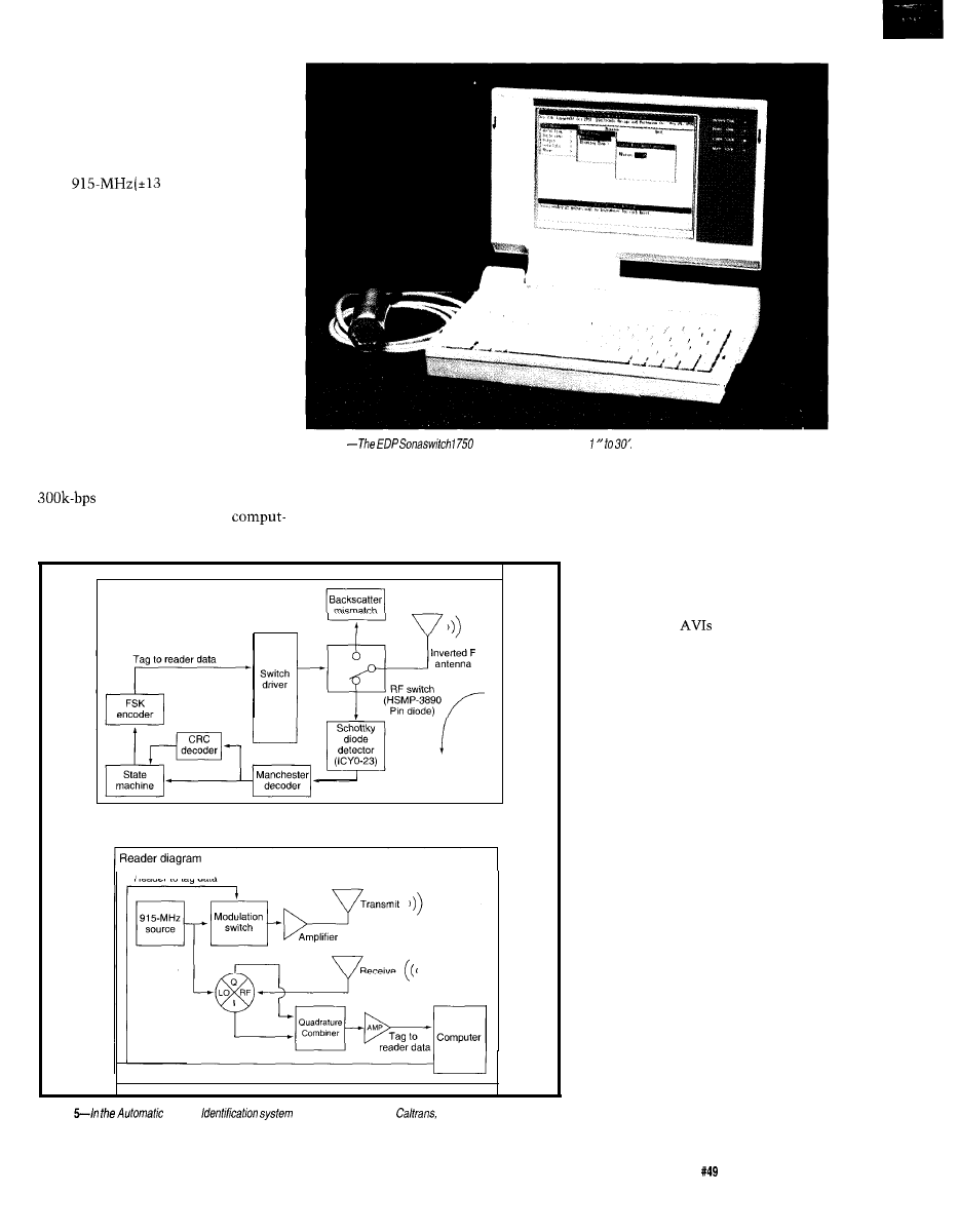
an “Automatic Vehicle Identification”
(or “AVI”) system.
As shown in Figure 5, the system
consists of a roadside “reader” that,
despite its name, supports both reads
and writes with a car-mounted “tag”
via a
MHz) RF link. The
tag uses a “backscatter” approach in
which the incoming RF is bounced
back to carry the tag’s response. This
reduces cost by eliminating the need
for an RF generator in the tag. It also
improves performance since the
response frequency (i.e., that generated
by the reader) is known exactly, which
wouldn’t be the case if each tag had its
own clock subject to variable toler-
ances and drift. Furthermore, the
system is frequency “agile” in the
sense that everything will still work if
a roadside reader’s frequency must be
Photo 1
measures distances from
changed to avoid interference.
Ultimately, it all adds up to a
read/write cycles (i.e., error correction)
bidirectional link between
per lane on a four-lane highway,
your wheels and Big Brother’s
nailing scofflaws traveling at up to 100
ers. This can support, for example, five
MPH through a one-meter RF “trap.”
Tag
block diagram
Reader to
tag data
Reader to tag data
Figure
Vehicle
being implemented by
a roadside “reader” can
both read and write car-mounted fags via an RF link.
RF tags are going to be a big deal,
not just for AVI
S
, but for all manner of
ID applications up to and including bar
code replacement. A detailed discus-
sion of the concept won’t fit here.
However, as a citizen and a driver, I
will take a few moments to pontificate
on the implications of AVI systems.
Ostensibly,
are our friends,
making life easier with automatic toll
collection, directions to the next
restroom, or whatever. What could
possibly be wrong with that?
Of course, the road to ruin is
always paved with good intentions.
To me, the situation is analogous to
the government’s attempts to “encour-
age” us to accept the so-called “Clip-
per” voice and data encryption
technology whose most notable
feature is that it gives the feds access
to the “keys.” But don’t worry, they
say, there are lots of “safeguards” and
we really just want to catch “bad
guys.” Trust us.
You’ve probably heard about the
roadside “candid camera” automatic
speeding ticket generators that use
radar to clock a car’s speed and snap a
picture of any hot rodders. Well, the
skeptics and paranoids among you
might easily imagine an AVI system
put to equally dubious use. Why, the
system could not only issue the
speeding ticket, but directly debit your
Visa card as well-no muss, no fuss.
The Computer Applications Journal
issue
August 1994
71
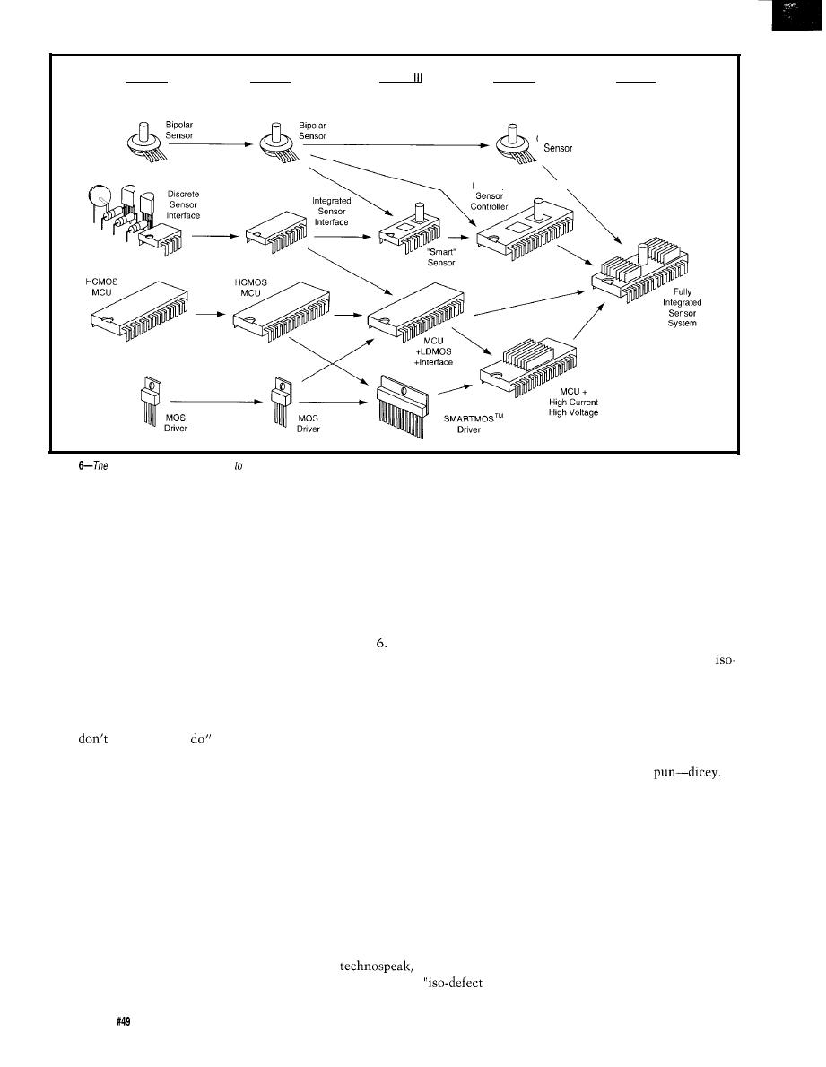
LEVEL I
LEVEL II
Discrete
Basic
Devices
Integration
LEVEL
Mixing
Technologies
LEVEL IV
Selective
Integration
LEVEL V
Full
Integration
MOS
Compatible
Multichip
\
Drivers
Figure
integration path from analog
digital for sensors can be broken down info five levels from discrete devices to full integration
OK, OK so you’ve got to slow
down whenever you spot a lurking
AVI-they aren’t going to be able to
blanket every inch of asphalt are they?
No, but should they draw the auto-
makers into the unholy alliance, it
wouldn’t be hard to “log” your bad
driving habits to later “tattle” when
you do pass an AVI.
However, an AVI-based “Officer
Speed” scheme suffers at the hands of
our justice system since it turns out all
you have to do is say you happened to
loan your car to “some person whose
name escapes me.” Yes, the good old
“cars
speed, drivers
defense
to the rescue.
If the system were only one-way
(i.e., tag data to reader), that would be
the end of it. But a two-way system
allows our leaders to take active
countermeasures. Maybe the same
“timeout” strategy used for obnoxious
kids is in order-if the AVI detects
your transgression, it can tell your car
to shut off, giving you time to contem-
plate the error of your ways.
Nobody knows how all this will
turn out, but I do predict that once we
let Big Brother into the driver’s seat,
he’ll be there for good.
OF SINKS, KITCHEN, AND HEAT
curve” that relates die size to yield.
Having started down the slippery
The curve is nonlinear because wafers
slope of combining analog sensors
are characterized by a certain defect
with digital intelligence, the question
density, no matter how many die they
is, where it will all end?
According to Motorola, the
integration path can be broken down
into five levels from discrete devices
(Level I) to full integration (Level V) as
shown in Figure
For many, many years we’ve used
and abused Level
I
techniques. Only
recently have Level II-III options, such
as those mentioned in this article,
emerged. Level IV-V devices remain
on the horizon for now.
Putting everything but the kitchen
sink on a chip raises a couple of issues.
Basically, what makes money and
what makes sense?
From the manufacturer’s point of
view, assuming integrating all the
goodies is possible, the concern boils
down to keeping die size near that
which provides optimal yields.
Most of you may be aware that die
cost doesn’t necessarily scale linearly
with size. A die with twice the area
may cost more than twice the smaller
device. In
the phenom-
enon is referred to as the
may contain. Thus, it’s easy to see that
a larger die has a higher probability of
running into a defect than a smaller
one. In the above example, the big die
might fail, but one of the two smaller
ones will make it.
If die size is small enough, the
defect issue becomes fairly moot.
Given, for example, 10 defects per
wafer, whether there are 200 or 300 die
per wafer matters relatively little.
Boost die size into the 50 or 100 die
per wafer range, though, and things
start to get-pardon the
From my (a user’s) point of view,
I’m all for ultimate integration since it
gives me the freedom to choose the
design-time versus unit cost tradeoff.
Naturally, I’ll use the availability of
lower-cost, less-integrated alternatives
to push the supplier to cut the highly
integrated unit’s price. Why should
I
care if it’s hard for the supplier to
make money on the “overintegrated”
unit? (Of course, I’d also be the first to
whine should they decide to quit
supplying the “unprofitable” part).
72
Issue
August 1994
The Computer Applications Journal
Otherwise, my only concern about
full integration is the migration of
high-voltage and high-temperature
functions on-chip at levels IV and V.
I’m sure the chip designers will be
careful to guard against IC meltdown,
while power consumption and thermal
management remain issues at the
system level, whatever the number of
chips inside.
Nevertheless, I’ve never really felt
comfortable with chips that are too
hot to touch, so talk of 40-W
tends
to make me a little nervous.
It seems likely that power,
voltage, and heat will remain a
dividing line with chips falling into
one of two camps. Since both camps
believe the sky’s the limit with
integration, many systems may
ultimately devolve to two chips. One
chip will be a big ugly metal thing
with lots of cooling fins or perhaps
even liquid or thermocouple “active”
cooling-dumb, but able to handle the
juice needed to make something
happen in the real world. The other
will be a high-pin-count, low-voltage
(3 V down to perhaps 1 V),
packaged Cray-on-a-chip that does all
the thinking.
q
Tom Cantrell has been an engineer in
Silicon Valley for more than ten years
working on chip, board, and systems
design and marketing. He can be
reached at (510)
or by fax at
(510) 657-5441.
Hewlett-Packard
Communication Components
Division
350 West Trimble Rd.
San Jose, CA 95131-1096
(408) 4354303
Fax: (408) 4354303
LLNL Transportation Program,
L-644
Lawrence Livermore National
Laboratory
Box 808
Livermore, CA 94550
(510) 423-4497
Fax: (510) 423-9649
Motorola Semiconductor Products
Sector MD
3102 North 56th St.
Phoenix, AZ 85018-6606
(602)
Fax: (602) 952-4067
AMP, Inc.
Piezo Film Sensors
P.O. Box 799
Valley Forge, PA 19482
(215) 666-3500
Fax: (215) 666-3509
EDP
37666 Amrhein
Livonia, MI 48 150
(313) 591-9176
Fax: (313) 591-7852
419 Very Useful
420 Moderately Useful
421 Not Useful
LCD PANEL METER
-Available now at an unheard of
N e w !
N o t s u r p l u s !
S p e c i f i c a t i o n s :
in
Maximum input:
additional ranges provided through
external resistor dividers
Display:
LCD, 0.5 in. figure height,
jumper-selectable decimal point
Conversion: Dual slope conversion, 2-3
readings per sec.
Input Impedance:
ohm
Power: 9-12 VDC 1
DC
Circuit Cellar, Inc.
4
Park Street, Suite 12, Vernon, CT 06066
Tel: (203) 875-2751
Fax: (203) 872-2204
NEW! UNIVERSAL DALLAS
DEVELOPMENT SYSTEM from
It’s a complete single board computer!
One board accommodates any 40 DIP DS5000, 40 SIMM
DS2250, 40 SIMM DS2252, or 72 SIMM DS2251, 8051
processor! Snap one out, snap another in.
Programs via PC serial port. Program lock & encrypt.
LCD interface, keypad decoder, RS232 serial port, 8-bit
ADC, four 300
relay driver outputs.
Power with
regulated or 6-13 VDC unregulated
Large prototyping area, processor pins routed to headers
Optional enclosures, keypads,
everything you need
BC151 Pro BASIC Compiler w/50+ Dallas keywords $399
TEL:
801.534.1017
FAX:
801.534.1019
555 South 300
East, Salt Lake City, UT, USA
841
The Computer Applications Journal
Issue
August 1994
73
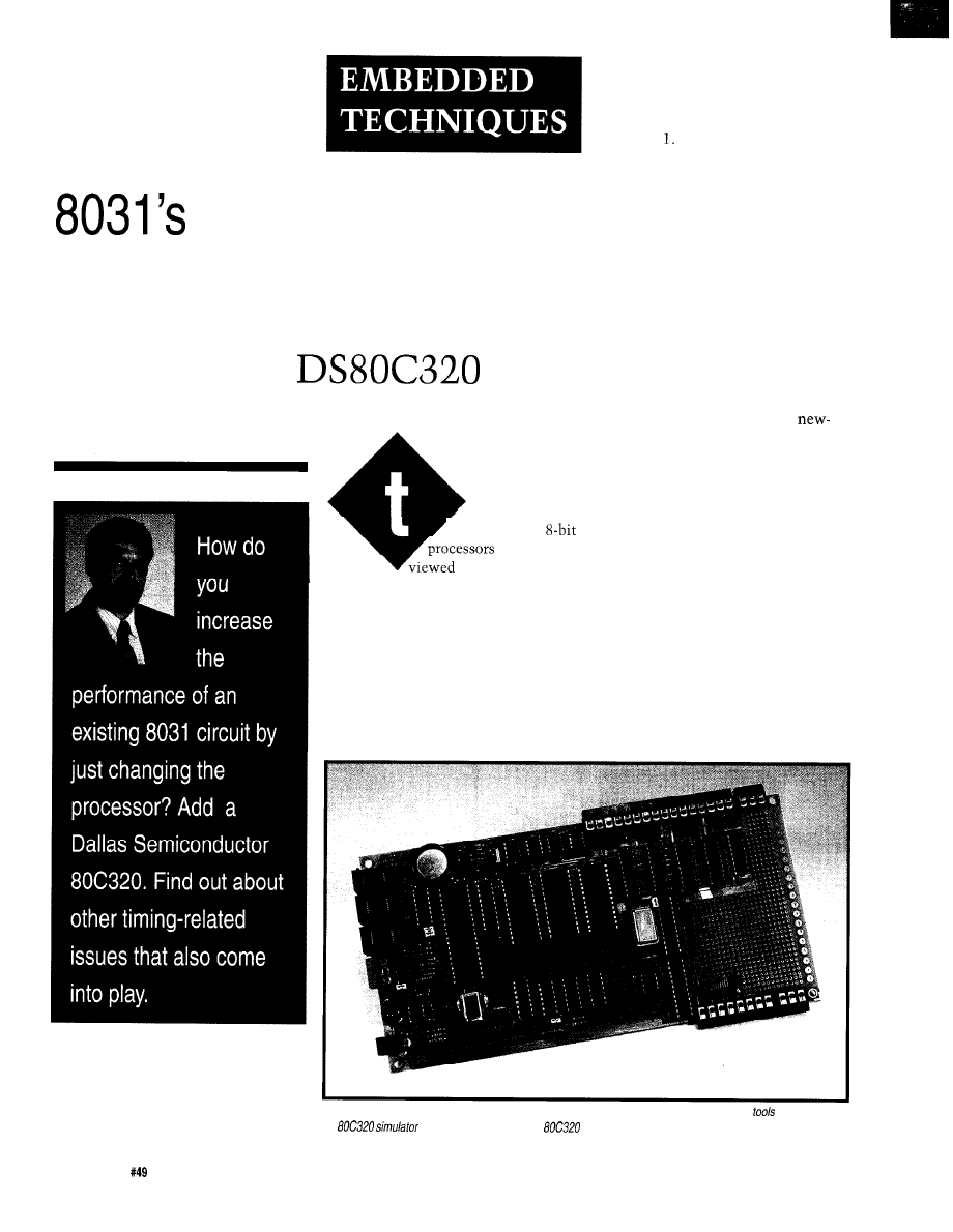
Speed
Demon in
Clothing
John Dybowski
Exploring the
Processor
, he proclamation
of the death of
could be
as a classic
example of a high-profile blunder.
Maybe it seemed like a safe call at the
time, but whoever made this state-
ment had little understanding of the
dynamics at work in the embedded
arena. Then again, if you’re of a more
cynical bent, you might suspect that
there lies a more sinister motive
behind what they were telling you.
As an example, I still remember in
amusement how hard Intel tried to
convince everyone that their 8096
architecture was the logical successor
to the 805 They even went so far as
to provide a code translator that
would, presumably, take your 805 1
application and translate it into 8096
code. The fact that the two chips had
memory and I/O models that were
completely different and that the 8096
maintained no continuity with
anything that came before it appar-
ently didn’t deter them. Most people
saw this as a ridiculous marketing ploy
intended to sell them a more expen-
sive processor than they needed or
wanted. It didn’t work.
The basic 803 1 is still a viable
candidate for new designs, and
and-improved derivatives based on this
fundamental architecture promise to
safeguard your investments well into
the future. Obviously, this is what it’s
all about. With the massive invest-
ment in development equipment,
substantial firmware libraries, and an
enormous working knowledge of the
8031 many engineers possess, it would
be very difficult, indeed, to move away
from any such “standard” architecture.
This is especially true if the architec-
ture is perfectly adequate for the task
at hand. But for every 8031 user that is
satisfied with the basic 8031 feature
set, there’s someone who needs a little
more performance or additional
Photo l--The ec.32
high-speed processor comes with an extensive set of PC-hostedsoffware
that includes
an
and monitor/debugger, and
cross-assembler, and a C cross-compiler.
7 4
Issue
August 1994
The Computer Applications Journal
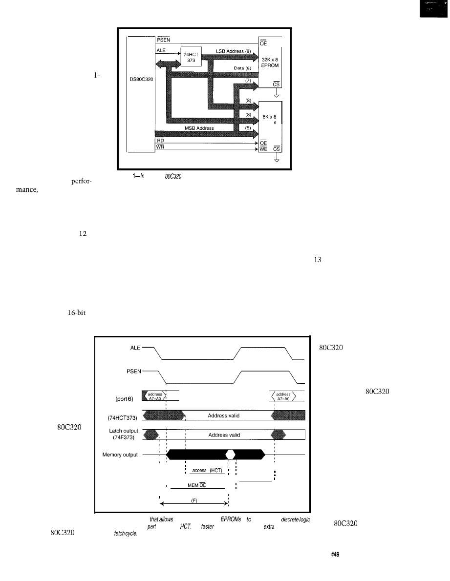
functionality. These needs
don’t go unfulfilled for long
since there’s always some
manufacturer willing to up
the processing ante.
Truly impressive 803
based derivatives are being
continually developed that
provide specialized built-in
peripheral sets that
are
well
suited for a number of specific
SRAM
applications. As far as
performance goes, most
manufactures simply boost
the basic clock rate, in some
cases, beyond 40 MHz.
Although this is one way of
getting additional
it would make sense
to first fix the execution core
before throwing faster clock cycles at
the problem. And if you don’t think
the 8031 is broken, how do you
explain that it takes oscillator
clocks to choke out a machine cycle?
And what about those instructions
that contain clocks that do nothing?
This is where the story takes a
bizarre twist. It turns out that the
processor I’m about to tell you about,
though based on the S-bit 803 1, attains
a level of performance that allows it to
give some of the
machines on
the market a run for their money. And
it shows that given
operates all the way from DC to 25
MHz. More importantly, the machine
cycle, which is a processor’s basic unit
of timing, now consumes only four
oscillator clocks instead of twelve as
with a conventional 803 1. In addition,
wasted cycles have been removed,
streamlining certain instructions.
All instructions run faster, but
some realize more of a performance
gain than others. Typical applications
should see a 2.5 times speed improve-
ment using the same code and same
crystal. Stepping it up a bit, at 25
MHz, a single-cycle instruc-
tion executes in as little as
160 ns. This is where
architectural refinement pays
off since it results in an
apparent execution speed of
62.5 MHz, which works out
to about 6 MIPS. Admittedly,
these 6 MIPS are made up of
tiny, little instructions, so
take it as a relative, not an
absolute, figure. Surprisingly,
with the multitude of
derivatives that had been
introduced since the 8031’s
inception, it’s taken this long
to get any real architectural
progress. If you’ve been
avoiding using a language
compiler on the 803 1 because
of performance concerns, your case has
just gotten a lot weaker.
Other new features include dual
data pointers, a second full-duplex
serial port, built-in power-on reset,
watchdog timer, power-fail interrupt,
and a total of interrupt sources (six
external).
Figure
a typical
setup where, for
simplicity’s sake, the EPROM
chip select is tied active, the EPROM access time is primarily determined by its
address access time parameter.
enough raw process-
ing power, you can
overcome such
seemingly insur-
mountable deficien-
cies as a meager
instruction set.
GO FASTER
Dallas Semicon-
ductor’s new
addresses a number of
performance-related
issues plus adds a
number of new
features to the
familiar 803 1.
Actually, it’s based on
the 8032, which
contains 256 bytes of
internal RAM and a
third timer. The new,
high-speed
Latch input
Latch output
IT’S ALL IN THE TIMING
By
now, experienced engineers
may be wondering what these perfor-
mance gains are going to cost them.
The cost I’m talking about goes
beyond the price
premium that the
exacts and
involves system-wide
concerns. Obviously,
there are going to be
timing-related ques-
tions since the
runs faster than a
standard 803 1, even at
a given crystal fre-
quency. And to really
tap its potential, many
people will run it at
maximum speed.
Cranking up the clock
rate implies tradeoffs
involving logic fami-
lies, memory and
peripheral costs, and
power consumption.
When considering a
new
design,
one of the first things
MAX MEM address
MAX MEM hold
time
MAX
access
MAX MEM address access
Figure 2-One
alternative
the use of lower-cost
is speed up the
path by using an f-series
in p/ace of
Jhe
parts give fhe EPROM
time during a
program
The Computer Applications Journal
Issue
August 1994
7 5
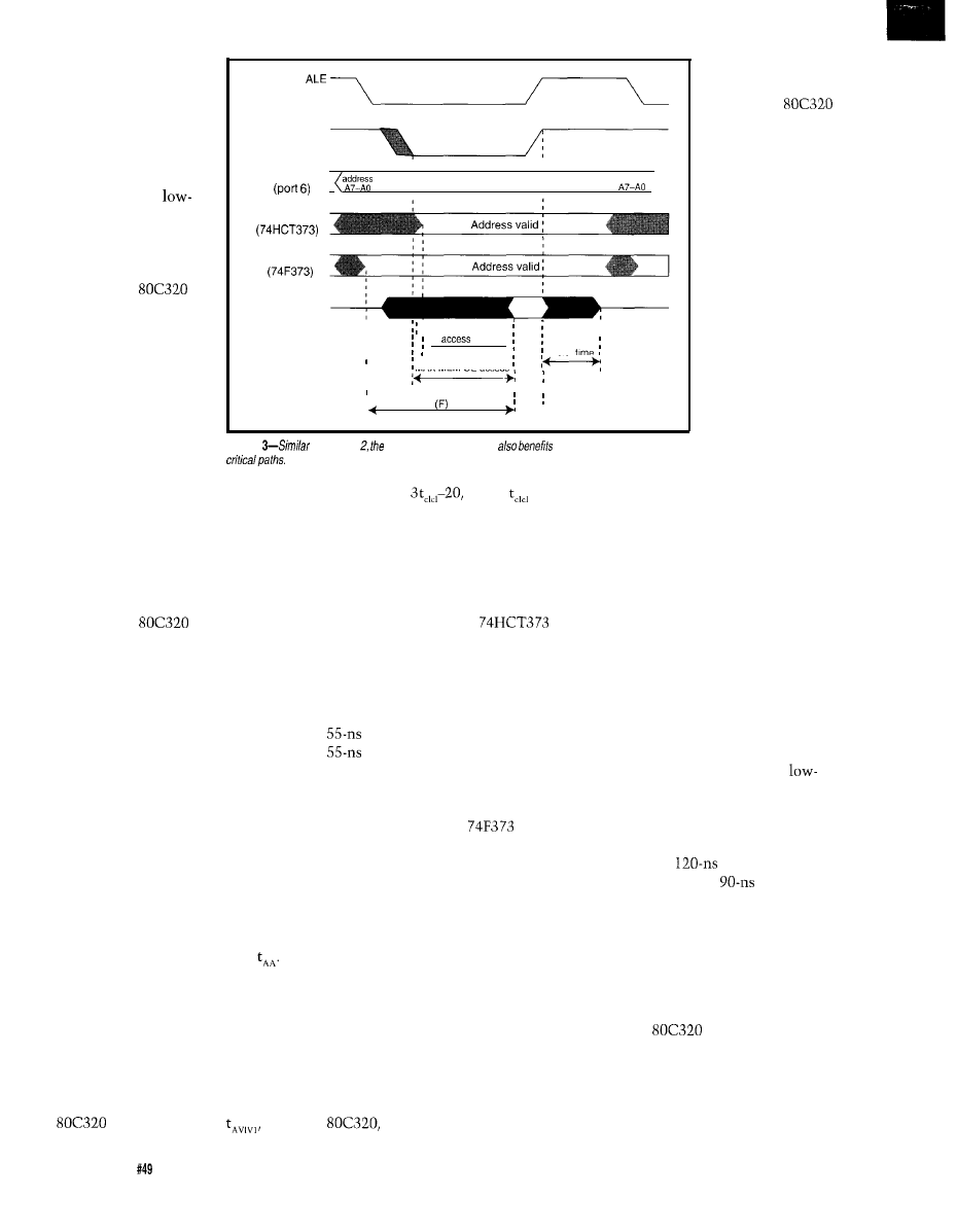
you’ll need to know is
the boundary fre-
quency at which
faster-and more
expensive-memory
components are
required, and the point
at which a truly
power design becomes
difficult to attain.
Existing applica-
tions can be enhanced
by using the
as
a drop-in replacement
for the 803 1. Since the
instruction execution
time is faster, there is
less time available to
transfer data to and
from memory. Al-
though it’s true that,
for a given clock speed,
PSEN
Latch input
a d d r e s s
Latch output
Latch output
Memory output
MAX MEM address
( H C T )
MAX MEM
hold
MAX MEM OE access
MAX MEM address access
Figure
to Figure
data memory read timing
from using F-series logic in
there is less time for
memory access, the problem may turn
out to be negligible for many systems
running at 12 MHz or less. For ex-
ample, a standard 8031 running at 12
MHz has an address access time
(neglecting any delays in the support
circuitry) of 300 ns. The corresponding
figure for an
running at the
same frequency is 230 ns. Take this
with a grain of salt, however, since we
really can’t afford to neglect any delays
in the support circuitry, as I’ll demon-
strate in short order.
Shifting our attention to the upper
frequency extreme, things become
more constrained. Since a memory’s
read timing usually proves to be more
restrictive than its write timing, I’ll
look at an instruction fetch cycle first.
For simplicity, let’s consider a hypo-
thetical bus configuration where the
EPROM has its chip select pin perma-
nently enabled (see Figure
1).
In this
arrangement, the access time is
primarily determined by the EPROM’s
address access time parameter,
The limiting factor in this timing path
is the time it takes the low-order
address to propagate through the
transparent address latch.
is defined as
where
is the
oscillator clock period. With just 100
ns available for the data transfer,
you’ve got to take a hard look at the
propagation delays in your support
circuitry. Naturally, these delays are
dependent on the logic family you
choose. Using a CMOS
would introduce a maximum propaga-
tion delay of 45 ns. This amounts to a
fairly substantial proportion of the
overall time available for access and,
consequently, requires the use of a fast
EPROM. Although you can get
EPROMs, they’re not common,
which means they’re costly.
An alternate approach is to use a
faster technology for the address latch,
A safe bet would be a
with a
worst-case propagation delay of 8 ns.
This results in a address access
requirement of 92 ns that is much
easier to satisfy while staying on
budget. Figure 2 is a simplified timing
diagram of a program fetch cycle.
At 25 MHz, an instruction must
be read into the processor within 100
ns from the time at which the address
is emitted. This is dictated by the
timing parameter
which
When beginning a new design, I
always like to start by analyzing the
timing relationship between the
processor and all the memory and I/O
components on the bus. With most
conventional 8031 designs, this results
in a somewhat academic activity since
seldom do I encounter any surprises.
To anyone considering using the
particularly if the system is to
76
Issue
August 1994
The Computer Applications Journal
run at higher speeds,
I would urge you to
look to the
and all of the
memory, peripheral,
and logic timing in
some detail. It’s
alarming to see how
some engineers have
grown complacent
about timing issues
just because they’ve
been working with
“safe” processors for
a long time.
There are many
different logic
families available
that are suitable for
use in high-speed
systems. Some are
more conducive to
low-power operation
than others. Regardless of the choice,
faster operation unquestionably means
higher power consumption. There are
tricks you can use to keep the power
consumption in check, such as
running the processor intermittently
using idle or stop mode, for instance.
The effectiveness of such tricks is very
much dependent on the technology
you select for your glue circuitry.
Unfortunately, you compromise your
potential power savings once you leave
the domain of a full CMOS design.
An attempt to delimit where the
performance/power boundaries fall
indicates that an economical,
power design can be rendered in
CMOS if you keep the oscillator
frequency under 16 MHz. This implies
a relatively conventional implementa-
tion using a
EPROM. If you’re
willing to opt for a
EPROM, then
the limit for full CMOS design falls at
about 18 MHz. Once you exceed this
range, you leave the realm of what can
economically be attained using
conventional HCT logic.
ACCOMMODATING TIMING
The
references its pro-
gram storage at a fixed rate. This rate
is based exclusively on the oscillator
frequency and, as a result, imposes a
fixed timing constraint on the system
program memory. The only way to
slow down the program memory
accesses is to use a lower crystal
frequency. Unlike program memory,
when performing external data
accesses, the
has a special
feature that allows the application to
control the access speed via a
speed MO V X instruction. The
can perform a MOV X in as little as two
instruction cycles. This interval can be
extended, if needed, all the way to nine
cycles. Although it’s true that fast
RAM is easier to come by than fast
PROM, the problem is that a lot of
memory-mapped peripherals are not
fast. Even if a fast system is required,
the peripherals usually don’t have to
be fast, and fast RAM might not be
necessary either unless the processor
spends a significant portion of its time
accessing data memory.
The processor can be instructed to
stretch its read or write strobe by
specifying a stretch value of between
one and seven. The use of stretch
cycles (or wait states), which widen
the read or write strobe, gives the
memory or peripheral more time to
respond. These stretch cycles can be
dynamically controlled by firmware if
slower devices are being accessed. The
stretch value is selected using the bits
in the Clock Control SFR
(special function register) located at
8Eh. On power-up, the
defaults to a one stretch cycle for
systems with slow data memories.
The timing requirements for
external data memory are similar to
those for the system PROM except
that stretch cycles can be introduced
to accommodate slower devices. For
example, an HCT-based system
running at 12 MHz would typically
require a
RAM with zero
stretch cycles, but could run with a
200-ns device with one stretch cycle.
At 16 MHz, still in HCT CMOS, the
corresponding figures would be 120 ns
and 200 ns, respectively. A system
using FAST logic operating at 25 MHz
would require an 80-ns RAM with zero
stretch cycles, but could get by with a
part with one stretch cycle.
Figures 3 and 4 illustrate the basic data
memory read and write timings.
At this point, some readers might
be wondering what fringe effect these
stretch cycles have on the access cycle.
In other words, what happens to the
setup and hold times? These are
certainly valid concerns since you can
extend the read or write strobes
indefinitely, but if you are unable to
meet the setup and hold times of your
particular device, you’re out of luck.
And the setup and hold times get tight
at 25 MHz, which could render a lot of
your favorite peripheral chips useless;
that is, unless you could buy yourself a
little extra time.
Early
data sheets gave
little clarification on these important
timing aspects, but more recent
documentation reveals that the
introduction of stretch cycles does, in
fact, adjust the setup and hold times as
hoped. The term
represents the
time interval added for each stretch
cycle. Generally speaking, the value of
t
is increased by
(remember
is the clock period) for each additional
stretch cycle that is called out. Note,
however, that the first stretch cycle
does not follow the expected pattern of
adding four clocks to the strobe. This
first stretch, in fact, uses one clock to
create additional setup time and one
clock to create additional hold time.
The other two clocks are dropped into
the middle of the read or write strobe.
Subsequent stretch values have no
further effect on the setup and hold
times and instead are entirely used to
extend the strobe.
Considering the particular timing
parameters that are important in
rendering a high-speed computing
system economically, Dallas did their
homework on this one. Conversely, it
should be pretty apparent that the guys
who have been pushing the clock rate
of the original 803 1 core to inordinate
extremes haven’t done us any favors
for anything other than basic
chip systems.
Another timing-related area where
the
accommodates the
programmer is in the number of
oscillator clocks used to advance the
on-chip timers. Although the
is capable of using four clocks per
r
L
Test your Logic circuits with
the printer port of your IBM
or compatible computer!
5 Input capture channels via printer port
q
High Speed 64K input capture buffer
El Glitch capture and display
Full triggering on any input pattern
Automatic time base calibration
4 cursors measure time and frequency
Save, print or export waveforms
The Real Logic Analyzer is a software package that converts an IBM or compatible computer
into a fully functional logic analyzer. Up to 5 waveforms can be monitored through the
standard PC parallel printer port. The user connects a circuit to the port by making a simple
cable or by using our optional cable with universal test clips. The software can capture 64K
samples of data at speeds of up to
(Depending on computer). The waveforms are
displayed graphically and can be viewed at several zoom levels. The triggering may be set to
any combination of high, low or Don’t Care values and allows for adjustable pre and post
An automatic calibration routine assures accurate time and frequency
measurements using 4 independent cursors. A continuous display mode along with our high
speed graphics drivers, provide for an’ “Oscilloscope-type” of real time display. An optional
Buffer which plugs directly to the printer port is available for monitoring high voltage signals,
Requires 286, or higher with EGA
VGA
Tel:
61 Piper Cr.
Software Only
Fax:
Kanata, Ontario
C a n a d a
Test Cable
Buffer
The Computer Applications Journal
Issue
August 1994
77
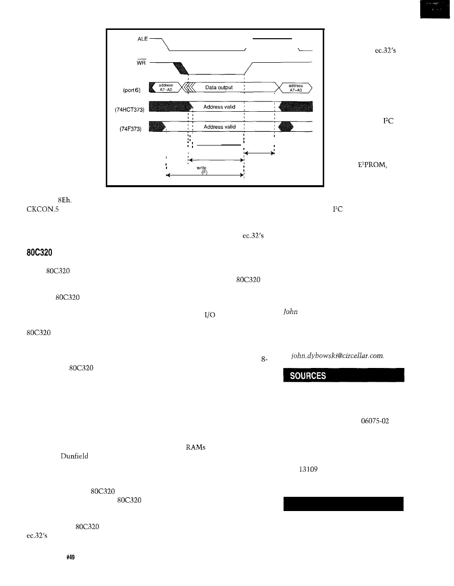
timer tick, the default
value is twelve, just
like the 8031 and
8032. This allows you
to calculate your baud
rate divisors and other
timer parameters in
the conventional
manner you’re
accustomed to. If you
need higher timer
resolutions, the speed
of any of the timers
can individually be
adjusted higher. The
control bits are
contained within
CKCON (the Clock
Control Register)
located at
controls
Latch input
Latch output
Latch output
MAX MEM write from
a d d r e s s ( H C T )
I
MIN data hold
MAX MEM write to data
MAX MEM
from address
Figure 4-/n addition to program fetch and data memory read cycles, the data memory write timing is
simplified by using fasf discrete parts
the speed of timer 2, CKCON.4
controls timer 1, and CKCON.3
controls timer 0.
TEST FLIGHT
A processing engine as advanced
as the
requires a test chassis
equipped with matching capabilities.
We’ve already established the superior-
ity of the
architecture as a
drop-in replacement for an 8031 in a
given application. At the other
extreme of the performance band, the
can be cranked all the way up
to 25 MHz. But a fast processor buys
you nothing unless you have a suitable
peripheral set to do some useful work.
Since the
will, doubtless,
find its way into applications such as
process control and data acquisition, it
follows that including the support
functions necessary to satisfy these
applications goes a long way toward
showcasing the processor’s capabilities
in a realistic manner. To satisfy this
need, Mid-Tech Computing Devices
has embarked on a joint development
effort with
Development
Systems. The results are the ec.32
high-speed processor (Photo 1) and an
extensive set of PC-hosted software
tools that include an
simula-
tor and monitor/debugger, an
cross-assembler, and C cross-compiler.
Rest assured that I will complete my
overview of the
and cover the
hardware and firmware in
detail in upcoming columns, but since
I’m almost out of space, let me leave
you with an overview of the
principal features.
THE EC.32 HIGH-SPEED
PROCESSOR
The ec.32 includes an
processor running at 25 MHz that
supports the primary analog/digital
peripherals directly on its high-speed
bus. The digital
section includes
16 TTL inputs; 8 TTL outputs; and 8
high-voltage, high-current Darlington
outputs. Analog I/O is supported with
a 4-channel ADC and a 4-channel
DAC. These are high-performance
bit devices that operate over a voltage
span of O-2.5 V. The ADC performs a
conversion in 3.6 us and has the
capability to sample all four channels
simultaneously. The DAC offers a 6-us
settling time and can update all of the
outputs simultaneously.
The system has 32K of EPROM,
32K of data RAM, and 32K of program
RAM. All
are backed up using a
high-density capacitor power source.
Possessing some of the desirable
attributes of a battery, this “supercap”
exhibits no wear-out mechanism and
doesn’t require any maintenance. The
program RAM permits users to
download executable programs from a
host computer and allows the resident
monitor to set breakpoints and to
perform program modifications from
the console. Access to
the monitor is nor-
mally via the
secondary RS-232 port,
leaving the primary
serial port (RS-232 or
RS-485) free for
applications.
The secondary
peripheral set is
supported on an
bus. Locally, this bus
connects a real-time
clock, 256 bytes of
nonvolatile RAM, 5 12
bytes of
and
a fully programmable
interval timer that is
set up for use as an
interrupt source. The
bus is carried
through to a connector where external
peripherals can be attached.
Finally, an efficient switch-mode
power supply provides 5 V to the
system and tolerates an input range of
8.5-28 VDC. Unlike a simple pass
stage, this supply doesn’t double as a
heater. And the wide input range
works well in a centrally powered
configuration.
q
Dybowski is an engineer in-
volved in the design and manufacture
of hardware and software for indus-
trial data collection and communica-
tions equipment. He may be reached
at
For elements of the project, contact
Mid-Tech Computing Devices
P.O. Box 218
Stafford Springs, CT
18
(203) 684-2442
Individual chips are available from
Pure Unobtainium
Old Creedmoor Rd.
Raleigh, NC 276 13
Phone/fax: (919) 676-4525
.
422 Very Useful
423 Moderately Useful
424 Not Useful
78
Issue
August 1994
The Computer Applications Journal
The Circuit Cellar BBS
bps
24 hours/7 days a week
(203) 871-l 988-Four incoming lines
Internet E-mail:
Reliability testing can be the bane of any electronic design. Getting
the circuit to work is one thing, but keeping it working in the real
world can be quite another. our first thread this month, we look at
some design techniques that can be applied your next circuit to
allow it withstand transient voltage tests.
Next, we move over the world of telephones with a
discussion about how to do call progress monitoring. While the
human ear can do it effortlessly, it’s not always that easy to do it
electronically.
Switching to the software side of things, converting between
infix and postfix notation is something most any compiler must do,
but knowing how do it is a prerequisite to writing that compiler. We
discuss some tips.
Finally, while Tom
talks about automatic vehicle
identification in his “Silicon Update” column this month, what about
having the computer take complete control of the car, allowing the
driver to
fake a nap? Our last discussion looks brief/y at
what’s been proposed for making such a system a reality.
High-voltage protection
From: GARY OLMSTEAD To: ALL USERS
am developing a system that will (probably) be
required to pass
Standard for Industrial Control
Equipment. I am concerned about passing the Transient
Voltage Test described in paragraph 59. It says that a single
pulse will be applied.
I assume that it may, or will, be applied to any pin that
comes to the outside world (although the standard doesn’t
say anything about this). I have protected the analog inputs
with an
combination, but I also have a
output and an RS-485 communications circuit. I
can put an MOV across them, but the current-limiting
resistor can’t be used.
How do you protect these points?
From: GEORGE NOVACEK To: GARY OLMSTEAD
A piece of cake. Well, not really, but it’s not as difficult
once you have done it the first time and understand the
mechanics. I am not familiar with
specifications, so
you’ll have to let me know what it is. The “5
means nothing unless I know the impedance of the tran-
sient generator.
There is one word of caution, however. Most designers
make the mistake of designing their circuit from the
functional standpoint first and only then start worrying
about EM1 and/or transient protection. You have to do it
the other way around. You start with the protection circuits
you will need (of course it is not a completely isolated
process; you keep the functionality in mind) and only when
you have it do you design the function. You may have to go
back and forth a few times, but I can guarantee that if
treated as an afterthought, no protection will work very
well in tough environments.
From: DAN HOPPING To: GEORGE NOVACEK
Well put, George.
I want to put a large
at the end of George’s state-
ment. I have been involved with medical equipment
hardware design for years and there were major problems
with *every* piece of equipment that left the component
protection (and isolation) as an afterthought. On the other
hand, when it was designed in at the beginning (i.e., the rest
of the circuit is built up around the required protection
scheme) the protection and isolation testing required at the
end of the project *always* went VERY smoothly. Like the
guy in the oil commercial says,
can pay me now..
you can *PAY ME* later!” All you youngsters who claim to
“want to learn” ought to tape George’s statement to your
design bench.
From: JOHN
To: GARY OLMSTEAD
Well, we use
as the series resistors on
our RS-485 inputs, which are then clamped with
back zeners as follows:
82
Issue
August 1994
The Computer Applications Journal
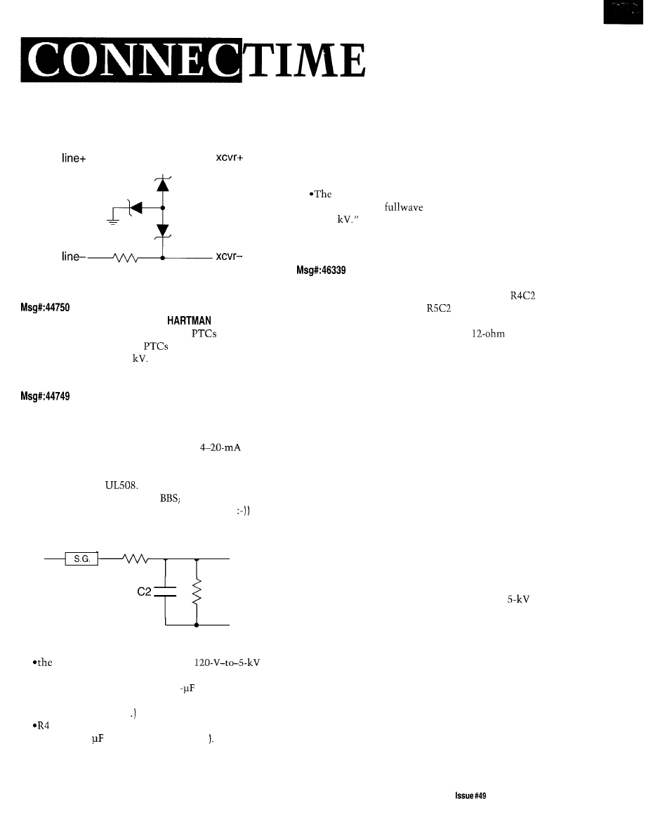
PTC
.
PTC
From: GARY OLMSTEAD To: JOHN
Yes, I asked Raychem about using
in that
application. They said their
are only rated to 600 V
and they won’t survive 5
Raychem specializes in the
telecom market and only has to worry about UL1489.
From: GARY OLMSTEAD To: GEORGE NOVACEK
Well, it really doesn’t matter too much which part of
the circuit is designed first: the input just feeds an ADC,
and the output is either a DAC feeding a
output or
an RS-485 link. Either way, starting over isn’t much of a
problem.
Anyway, on to
I’m really looking forward to
being able to send graphics to a
it would be a lot
easier... (Say, maybe there’s a product idea there.
Here
goes:
R 4
R5
Gnd
where:
is 12 ohms, wirewound, wound to reduce reactance.
stuff to the left of the input is a
l
C2 is 0.07 (yes, 0.07: 2 x 0.01 + 0.05
converter. It reduces, more or less, to a 10-M resistor
to ground in parallel with a 0.1
cap.
l
S.G. is a spark gap (“employing boiler electrodes,”
l
R5 is 350 ohms (300 watts!) I know you don’t need to
whatever they are..
know that, but stage one of the conversion is a neon
sign transformer. I’ve seen neon sign transformers, but
never one that made anybody think of 300-W resis-
tors. (Of course, maybe they just need it for the
voltage rating.)
output pulse is described as a “single 1.2 by 50
microseconds
impulse with a crest value of
5.0
Well, that’s it.
From: GEORGE NOVACEK To: GARY OLMSTEAD
That is a fairly standard transient generator.
determines the rise time and
the fall time of the
pulse. Also, R4 determines the maximum current you can
zap your circuit with. In this case, with
resistor, the
maximum current will be roughly 417 A. Nothing to sneer
at, but no big deal.
There are generally two types of tests: pin injection and
bulk injection. In pin injection the generator is grounded, as
is your enclosure, and then the generator discharges into
each pin of your connector (or wire, if you have just fly
leads). This is usually referred to as a damage tolerance
test,
since you want to make sure nothing gets fried.
In the bulk injection test the entire harness from your
box passes through a current transformer. When the
generator is discharged into the transformer, the entire
harness swings, injecting common mode transient into
your system. This is generally referred to as a functional
upset test.
You inject all kinds of pulses and single and
multiple bursts, examining what the system does. You
want to make sure that if the transients upset it, the upset
is benign and you also want to know how the system
recovers from it.
Your simplest protection of the circuit is to have either
a plastic enclosure or, if it is metal, then floating the
electronics inside it. The test is performed by applying the
transient between the ground-usually a large copper
Testing for damage tolerance between two pins is
highly unusual. If, for example, you have an RS-485 line, it
is a twisted pair. You do not test it by sticking a
pulse
between the two pins. In a lightning strike, for instance,
both lines are close enough to be at the same potential.
Sure, you can have a short on one line, but then you are
getting into a higher level of protection. Now, you are not
dealing with the environment, but with failures. You need
to consider, however, what is connected to your equipment.
You can have the best protection in the world just to be
blown out of the water if the other guy did not do his job
right.
The Computer Applications Journal
August 1994
8 3
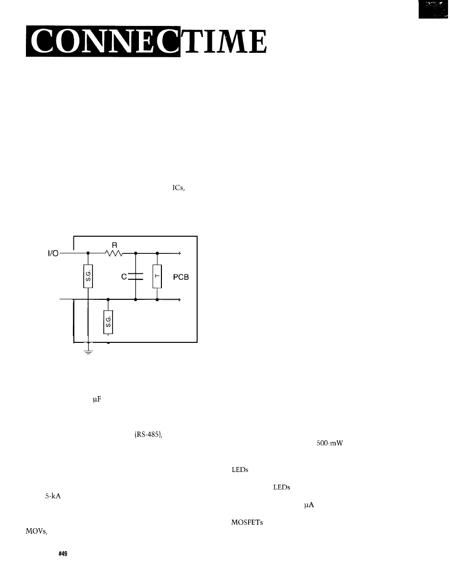
plate to which your equipment is fastened-and every
connector pin or lead coming out of your box. If the elec-
tronics are floating, then all you have to worry about is the
dielectric strength between the guts and the case. For the
most part it is a question of spacing if you have a metal
envelope.
You also want to make sure that the parasitic capaci-
tance between the electronics and the enclosure will not
allow high-voltage spikes to build on the lines. This is
easily prevented by capacitors, which should be on the
inputs for ESD protection anyway (you can buy
such as
RS-232 line drivers with the ESD already on chip). A typical
line (input or output) would look like this:
Cabinet
RTN
Here, R would be a small resistor, say 25 ohms on an
RS-485 line. On high-impedance inputs you can go a lot
higher (the higher the better). C should be as large as
possible, typically 0.1 on output lines. Again, you have
to make sure you are not limiting your system bandwidth.
The RTN (return) line should go through without a resistor
if it is actually your common potential of the electronics. If
not, such as with a differential pair
both lines
should have the RC elements, tied internally to RTN.
I would also use spark gaps (SG) between each line and
the cabinet. This will ensure that the potential between the
cabinet and the electronics will never exceed the flash-over
level. I use CP Clare’s dual spark gaps. They fire at about
200 V and the smallest ones (about 0.5” dia x 1”) will easily
take a
surge. In addition, the dual gaps, when used on
differential lines, will both fire at the same time, thus
preventing differential voltage buildup which could damage
the IC. They cost around $4 in quantities of 10. Unlike
they do not deteriorate with use.
You will always have a residual spike due to finite
turn-on time of the surge suppressors. This is where the RC
comes in. It is also a good idea to put a device between two
differential lines, be it inputs or outputs, to limit the
differential voltage between them. It is shown as T (for
transzorb), but can be many other devices. In the isolated
cabinet scheme you do not need to use these devices
between single input or output lines and RTN unless you
want to protect the line from overvoltage. The RC is
already taking care of those. Also, keep in mind that in this
scheme, any current due to transient injection flowing
between your electronics and the chassis ground is through
the spark gap (once fired, the voltage drop will be about 20
volts) and some parasitic capacitance between the line and
the chassis. Consequently, the current will be a narrow,
low-energy spike which any quarter-watt resistor in place of
R will handle.
It is unusual to require that this (isolated cabinet)
system take a hit or accept very high voltage between two
lines as opposed to a line and the chassis. If this is a
requirement, then you will have to protect the lines the
same as if the case were on the same potential as the
common potential of the electronics (internal ground).
To limit the voltage between two differential lines
(device T above), you have many options. For communica-
tions lines, the best choice is usually a bipolar transzorb. It
depends on the differential voltage you can allow and the
maximum current which would flow through the clamp.
For many current inputs where voltage difference would be
minimal, two parallel signal or rectifier diodes limiting the
voltage to 0.55 V will do. Or you can use back-to-back
zeners, although I prefer bipolar transzorbs, as they are
faster and take higher surge.
If the leakage is critical, using a reverse-biased P-N
junction of a PNP or NPN transistor (small-signal transis-
tors are best; leave the collector unconnected) gives you a
beautiful “zener” with an extremely sharp knee zeners can
only dream about at just few microamperes of current.
Leakage below that knee is hardly worth considering. They
will dissipate about the same as
zeners and their
zener voltage will vary between about 5 and 10 V, depend-
ing on the device (voltage of a device is very consistent).
in forward bias also make excellent zeners. Their
voltage will again depend on the type, starting from about 1
V to 3 V, with red
at the low end, followed by green
and yellow the highest. I used them once as a voltage
reference when I had only 2
to work with and no
commercial zener could do the job.
are also great. You connect drain and gate
together to the line, source to the return. With many
84
Issue
August 1994
The Computer Applications Journal
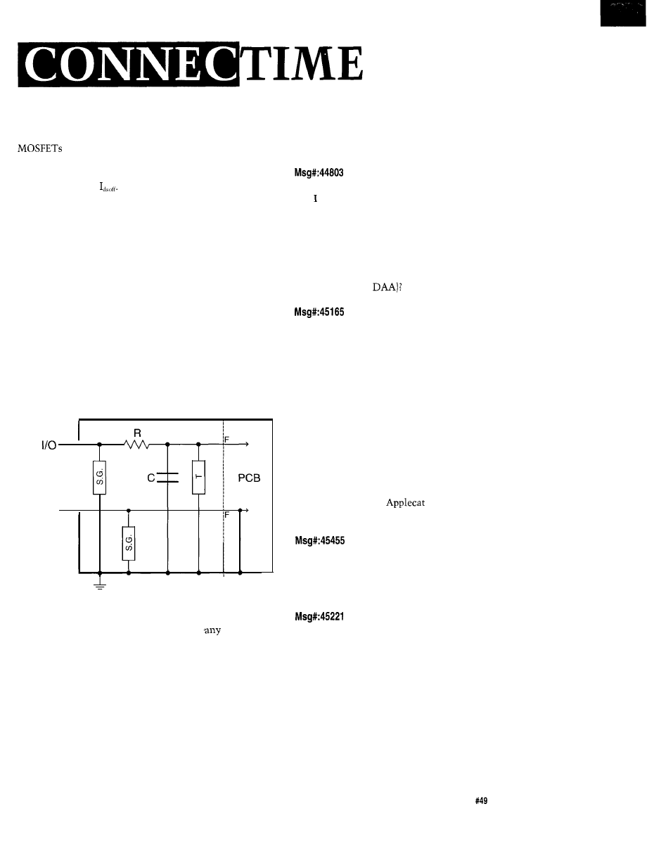
having a gate threshold voltage around 3 V,
you’ll have a nice, often powerful (depends on the FET)
clamp. And it will be bidirectional. The leakage will be
determined by the
I can’t think of one commercial application where you
would need to ground your electronics to the chassis
(cabinet). You generally have no other choice when you are
up against some onerous emission and susceptibility
requirements, which make it necessary to run your inter-
face with the world through feedthrough low-pass filters.
Their unfortunate shortcoming is they are rated for only
about 50 V. That means you have to cut the transients first,
then go through the filter into your electronics. The filters
are usually in a pi configuration, with capacitors grounded
to the chassis. You could have an isolated metal box within
another box, but this is expensive and heavy. The solution
is in using a dual cavity, but then the electronics ground
must be connected to the chassis ground. (If it was not,
you’d be getting some nice signal feedback through these
capacitors.)
Cabinet
RTN
Dirty
Clean
As you can see, the RTN is now internally connected
to the chassis. Spark gaps will take care of
voltage over
200 V and, once fired, clamp it to 20 V. In the second stage,
the transzorb T with resistor R cut the spike to, say, 5 V on
the RS-485 lines. On some differential lines you may want
to use three transzorbs: each line to ground and then one
between the lines.
Call progress detection
From: JAY SISSOM To: ALL USERS
am looking for an easy way to monitor what is
happening on a phone line. I need to know if the remote
phone is ringing, if the line is busy, if they picked up the
phone/hung up the phone, and so forth. My first thought
was to purchase a cheap modem, but I need to send audio to
the phone line and record from the phone line.
Does anyone know of a chip that does it all (and works
with an approved
From: BEN MEHLMAN To: JAY SISSOM
What you are talking about is called “Call Progress
Detection” and there are chips out there that do it. Since I
have no experience with any of them I won’t attempt to say
more on that score, except that you might want to check
out Cermetek, Harris, Teltone, and Motorola among others.
Another possible option for you is a software-driven
solution. You could couple the phone line (through some
simple shaping circuitry) to the serial port on a computer
(or to a pin on your microcontroller). But what I’m suggest-
ing is not to attempt to measure the frequency as some
have done, but rather to look at the timing of silence versus
sound on the line. Each type of signal has its own distinc-
tive rhythm. This is how it was done for call progress
detection on the old
modem. This really cuts your
hardware and software down to a minimum.
From: JAY SISSOM To: BEN MEHLMAN
Thanks for the message. That’s a good idea. I never
thought about measuring silences. I’ll have to play with it
to see if I can make that work!
From: RICHARD NEWMAN To: JAY SISSOM
Dialogic makes boards for PCs that can do everything
you want and more, however they are quite expensive:
about $250 per port and usually have 2 or 4 ports.
Is this in your price range?
If you want to build one yourself, it’s easy to do. You
can get a DTMF transceiver in a single package with call
progress detection included. You must validate the call
progress with software to derive specific signals (busy,
ringback, sit, voice, answer machine).
The DAA should have a duplexer so as to improve your
transceiver characteristics. (Being able to hear the DTMF
The Computer Applications Journal
Issue
August 1994
8 5
TIME
being sent to you while you are sending speech back to
very nicely. I believe they sell an SDK for it for $150. There
them.) The duplexer could be as simple as a transformer
may be others that come with an SDK or, better yet, just a
w h i c h w o u l d a l r e a d y b e U L t y p e a c c e p t e d .
documented interface, or perhaps a TSR with a documented
Digital speech recording and playback is simple to do
interface.
also. You need to make some decisions about fidelity versus
cost and storage space. If you need great fidelity, you’re
probably better off with a DSP. You can do ADPCM
encoding/decoding and reduce your bit rate considerably
Infix to postfix conversion
and then do compression to reduce storage requirements
even more. All of this in one DSP.
If your going to be satisfied with average fidelity and
From: SCOTT CHRISTENSEN To: ALL USERS
you don’t need to use a standard audio file format then
I am looking for source in C to convert from infix to
using a CVSD type part is cheap and easy. You can record
postfix. I envision input and output are strings. For ex-
one second of speech in 1500 bytes of storage and the audio
ample:
quality compares with a telephone line on a long distance
call.
In: 4 + 5 (2 + 1)
All of the software to drive this could be written in C,
and one piece of software could drive multiple cards in one
PC. It’s probable that one card could have several interfaces
Thanks.
on it also.
Your price range for a single-port card, if you built it
yourself, would probably be about $40 including a PC
From: DAVE TWEED To: SCOTT CHRISTENSEN
prototype card.
Ah, that brings back memories of college and the
From: JAY SISSOM To: RICHARD NEWMAN
Thanks for the message. Basically, I want to use a
board to do the recording and playing. I am
writing the user interface in Windows and do not want to
do low-level calls if I don’t have to. There are multimedia
drivers for the SB card, so I would like to use them. I want
to build a board that I can control with the serial port to do
the call monitoring. The $40 solution you were talking
about sounds good. Thanks for your help!
From: BEN MEHLMAN To: JAY SISSOM
If you must use the
you’ll definitely need
an external DAA which you can take on or off hook via a
control line on the serial port or parallel port. You can
detect call progress through silence detection and you can
generate DTMF for dialing out fairly easily. The only thing
that’s not totally straightforward is detecting DTMF in
software. But I question whether you are using the right
tool for the job.
Someone mentioned Dialogic boards which do every-
thing you want including the DAA. I have one and it’s very
nice, but expensive. There are cheaper boards if you only
need to handle one line (the Dialogic does four). A friend
has a $
voice mail board (including software! that works
compiler class. Every compiler has to do that conversion
and it was a basic exercise that we all had to write.
I don’t have source code for you, but I can tell you that
you basically need to set up a stack to hold the operators as
you scan them from the input string, and then a “prece-
dence table” tells you when to take things from the stack
and send them to the output string. The operands (numbers
or variables) are always passed through.
Be careful: the example you give seems to use “calcula-
tor precedence,” which is really no precedence at all-all
operators are equally important. Another translation of your
input string, using algebraic precedence in which multipli-
cation and division are done before addition and subtrac-
tion, would be:
This is part of the problem with infix notation-the
precedence rules need to be established separately. With
postfix (or prefix) notation, it is explicit, and you never need
parentheses to make it clear.
Let’s say you have a scanner that gives you one token
(operand or operator) at a time. As you scan the input string
left to right, you look at each token in turn and apply the
following rules:
1. If the current token is an operand, append it to the
output string.
86
Issue
August 1994
The Computer Applications Journal
2. If the current token is an operator, check the opera-
tor stack:
2a. If it is empty, put the operator on the stack.
2b. If the last operator on the stack has equal or higher
precedence than the current token, pop operators from the
stack and append them to the output string until you find
one with lower precedence or the stack is empty. Put the
current token on the stack.
3. If the current token is an open parenthesis, push it
on the stack unconditionally.
4. If the current token is a closed parenthesis, pop
operators from the stack and append them to the output
until you find the open parenthesis, then throw away both
parentheses.
5. If there are no more input tokens, pop any remaining
operators from the stack and append them to the output.
Note that rules 3 and 4 can be mostly implemented by
treating parentheses as operators and setting up the prece-
dence table so that the open parenthesis is the highest
possible precedence and the closed parenthesis is the
lowest. You still need to make sure you throw them away
rather than put them into the output string. The precedence
table will look something like one of these:
Algebraic
H i g h e s t :
Calculator
H i g h e s t :
Lowest:
Lowest:
This should get you going. The C code is left as an
exercise for the reader I did mine in PDP-11 assembly
language.
From: SCOTT CHRISTENSEN To: DAVE TWEED
Thanks, Dave. I started working on this yesterday using
a data structures book that talks about this. The thing that
may be a problem is multiple occurrences of operators in a
row. For example, 6 5 = This would of course be
illegal, but 6
l
-5 = would be legal. Differentiating this is
the fun part.
From: LEE STOLLER To: SCOTT CHRISTENSEN
From: DAVE TWEED To: SCOTT CHRISTENSEN
Yes,
I
wondered whether that was going to be an issue
for you. It’s really two problems: The scanner should deal
with literal numbers with leading sign digits, since the sign
really is part of the number (like -123). The other problem
Allen Holub has written a book, “Compiler Design in
C.” I haven’t read it, but from other books he has written, it
ought to be good. The man writes clearly with good ex-
amples. Try to see if you can borrow it from someone or
somewhere. It ought to have just what you need.
is really the
operator” problem, in which unary
(as in +
is really a one-operand prefix-type operator,
just like functions such as “sin x,” “logy,” and so forth.
The infix-to-postfix algorithm is really only for binary
(two-operand) operators; it is assumed that a parser has
already validated the string and dealt with the unary
usually by changing it into some other symbol analogous to
“change sign” (which is how most calculators deal with the
issue in the first place). So, your example would look
something like this:
Input: 6 * 5
After parsing: 6
l
CHS 5
After postfix conversion: 6 5 CHS
l
All of the unary prefix operators have a precedence
between and the binary operators; this causes them to
be transferred to the output string at the right time, while
still allowing things like:
sin ( x + y
to be turned into
x y sin
Just to cover all of the bases, if you should have any
postfix operators in the input string, like factorial
the
infix-to-postfix conversion should simply copy them
straight to the output when they occur in the input. So,
3 + IO!
would become
3 IO! +
and
(3 +
would become
The Computer Applications Journal
Issue
August 1994
87
From: SCOTT COLSON To: ALL USERS
A friend of mine has been asked to research Intelligent
Highway Vehicle Systems
She has no technical
background and asked me for a quick explanation of how
the system works. I have no idea how IHVS works so I was
wondering if anyone here might be able to direct me to a
source of information. I believe IHVS is used in those
automated toll booths but that’s all I know about it. I would
appreciate any info.
From: GEORGE NOVACEK To: SCOTT COLSON
From: BOB PADDOCK To:
COLSON
We looked into it some time ago. With the recession in
the aerospace industry and the defense cuts, the high-tech
companies were looking at what to do next. I’m not really
cognizant of the subject as it exists today. Undoubtedly a
lot of things happened since I looked into it. Basically,
freeways and throughways would be set up in such a way
that once the automobile gets on the ramp, a computer
takes over the control of the car. The passengers can
literally go to sleep until the car comes to the predestined
exit, where the driver is alarmed and takes over from the
computer.
If this is the same as Intelligent Vehicle Highway
System (IVHS) you might want to check out the June 1994
issue of Ward’s Auto World for “IVHS: A smart way to go:
Conference growth indicates blossoming industry” by Tim
Of course, two-way communications must exist
between the car and the system. Inductive control with a
cable buried in the road was considered as well as some-
thing similar to the cellular phone. Car spacing was to be
either controlled centrally by splitting the road into small
segments, as well as giving vehicles their own intelligence
by installing ranging devices on them. On the top level, one
had a computer system capable of routing thousands of
vehicles for their destinations at shortest, fastest, and most
efficient way.
We invite you call the Circuit Cellar BBS and exchange
messages and files with other Circuit Cellar readers. It is
available 24 hours a day and may be reached at (203)
1988. Set your modem for 8 data bits, stop bit, no parity,
and 300, 1200, 2400, 9600, or
bps. For information on
obtaining article software through the Internet, send
mail to
To maintain the safety (this is where the aircraft
companies could score), almost everything on the vehicles
was to be at least dual redundant, fail safe, with detected
faults forwarded through communications to the nearest
service depot, so that spare parts and maintenance crews
would be waiting by the time the vehicle arrived.
Software for the articles in this and past issues of The
Computer Applications
may be downloaded from
the Circuit Cellar BBS free of charge. For those unable to
download files, the software is also available on one 360K
IBM PC-format disk for only $12.
The big issue, of course, was software reliability (this is
a misnomer, but is being used], with the minimum
probability of failure (bugs]. All of the system software was
to be done in Ada according to avionic criticality level A.
The main computer was to be at least triple redundant,
with each of the three computers using a different processor
with software written by different teams to prevent any
To order Software on Disk, send check or money order
to: The Computer Applications Journal, Software On Disk,
P.O. Box 772, Vernon, CT 06066, or use your Visa or
Mastercard and call (203) 8752199. Be sure to specify the
issue number of each disk you order. Please add $3 for
shipping outside the U.S.
425
Very Useful
426 Moderately Useful
427 Not Useful
possibility of a common mode error. As you can see, a bug
could result in quite a carnage.
I don’t know where the project stands now. Some of the
first work was to be done in California and many aerospace
companies were interested. A lot of interest dried up when
it was indicated that this was not a government-funded
project, but that each company would do their R&D for
their nickel and hope to capitalize on it in the future from
commercial success. This might work when the times are
good. When companies struggle, there is little money left
for pie-in-the-sky speculation. This is where I was pulled
out of it.
Hope it helps.
88
issue
August 1994
The Computer Applications Journal
Time to Move On
just spent the last hour and a half on the Circuit Cellar BBS answering electronic mail. Coincident with the
physical posting of the magazine, asked Ken to put last month’s “Ciarcia Junk” editorial on the BBS as well.
Barely a day later, I’ve already got a dozen requests. Everybody is requesting a specific project box, but ultimately
they petition to receive virtually anything. The present requests range in scale from the earliest switching regulator project to the
processor Mandelbrot Generator, with no two appeals for the same project.
The fact that the first request was for the Mandelbrot Generator brought up the question of whether some projects were too
expensive to give away. If I remember correctly, it cost close to $12,000 to build. course today, with $150 486-25 motherboards
having equivalent power, the Mandelbrot box would sell by the pound. Obsolete hardware is just that, obsolete. OK, 60 Ibs into the
UPS box.
Processing these requests has generated some vivid recollections. While the hardware in these projects is significant because it
often marked a technological milestone, the fact that these projects were published so others could physically share the experience is
what makes them truly significant. If having a circuit kludge or noteworthy manuscript page tacked to your computer room wall helps
you remember that, so be it. I’m glad to help.
Ensuing technical events will probably be less dramatic, but no less important. We have witnessed a major evolution in computer
systems. Among the half dozen or so technical revolutions brewing, be prepared for similar advances in home automation and building
control technology. Of course, some people will be dragged kicking and screaming into this new world because our misinformed media
usually depicts home automation as something to do with expensive entertainment and stereo systems. How wrong they are.
If I had said the words “energy management” instead, the whole world of political correctness opens up. Add functional
embellishments like “security enforcement” and “lighting manager” and people want to know more.
The problem with political correctness in technical nomenclature is that such terminology beats around the bush. Functional
interrelationships are lost. If you have not realized the energy benefit of your air conditioner turning on two hours before you get home
rather than having it run all day because I call the $10 control module that accomplishes the task a home control device rather than an
energy management facilitator, I apologize. Political correctness is not my bag.
I recently came across a good videotape that may help many fence sitters better understand an electronically enhanced home.
Presented so that a novice can learn and a professional won’t get bored, “Living With An Intelligent Home” is a good introduction
describing current applications using today’s technology. This VHS tape retails for $24.95 plus $5 shipping, but is being offered to
for $17.95 plus $4 shipping (in U.S.). Call, fax, or write us and be sure to include the
subscriber number from your
Applications Journal mailing label.
Understanding new technology always benefits those who recognize and do something with it first. Next month give you an
opportunity to do both.
Issue August 1994
The Computer Applications Journal
Wyszukiwarka
Podobne podstrony:
więcej podobnych podstron