
7
9
25274 75349
0 5>
CIRCUIT
CELLAR
®
ww
ww
ww
..cc
iirr
cc
uu
iitt
cc
ee
llll
aa
rr
..cc
oo
mm
T H E M A G A Z I N E F O R C O M P U T E R A P P L I C AT I O N S
$4.95 U.S. ($5.95 Canada)
# 1 3 0 M A Y 2 0 0 1
MEASUREMENT AND SENSORS
Frequency Meter Metal Detector
Digital Yard-Stick
Anemometry
Goes Ultrasonic
Testing by
Simulation

Premier GPS Inc., (403) 295-8879, Fax: (403) 274-3021, tabsha@premier-gps.com
computer systems in tiny modules
DIP-type modules with 28 - 92 pins
cut consumption (50mA @ full speed),
cut components, cut system cost
Digital, analog and serial I/O channels in module
Expansion Bus for up to 4,096 I/O lines
160 kB ... 6 MB FLASH + SRAM, RTC, Watchdog
BASIC Tigers™ deliver what developers and manufacturers
really want:
Test the Tiger at no risk today.
http://www.wilke-technology.com
ANU-2001-01.pm6
19.02.01, 17:11
1
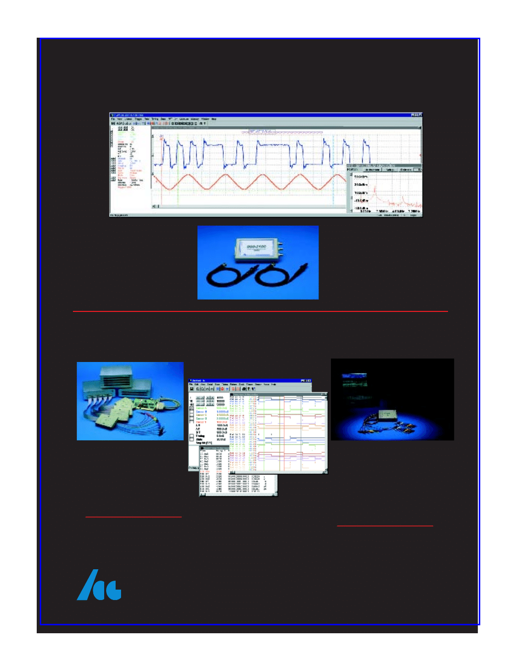
• 2 Channel Digital Oscilloscope
•
• Advanced Math options
• FFT Spectrum Analyzer options
Probes, Interface Cable, Power
Adapter, and software for
Win95/98, WinNT, Win2000
and DOS.
Optional 100 MSa/s Pattern Generator
LA2124-128K (100MSa/s, 24CH)
Clips, Wires, Interface Cable, AC
Adapter and Software
www.circuitcellar.com
CIRCUIT CELLAR
®
Issue 130 May 2001
3
Measurement and Sensing with the MPC565
Frequency Meter Metal Detector
Andrei Chtchedrine & Yuri Kolokolov
Behavioral Plant Simulation for Testing a Control
Algorithm
Return of the SBC
Multitasking Applications with SBC-386EX-S
The Company Formerly Known as Scenix
COLUMNS FEA
TURES
ISSUE
Advertiser’s Index
June Preview
Priority Interrupt
Steve Ciarcia
130
ChipCenter
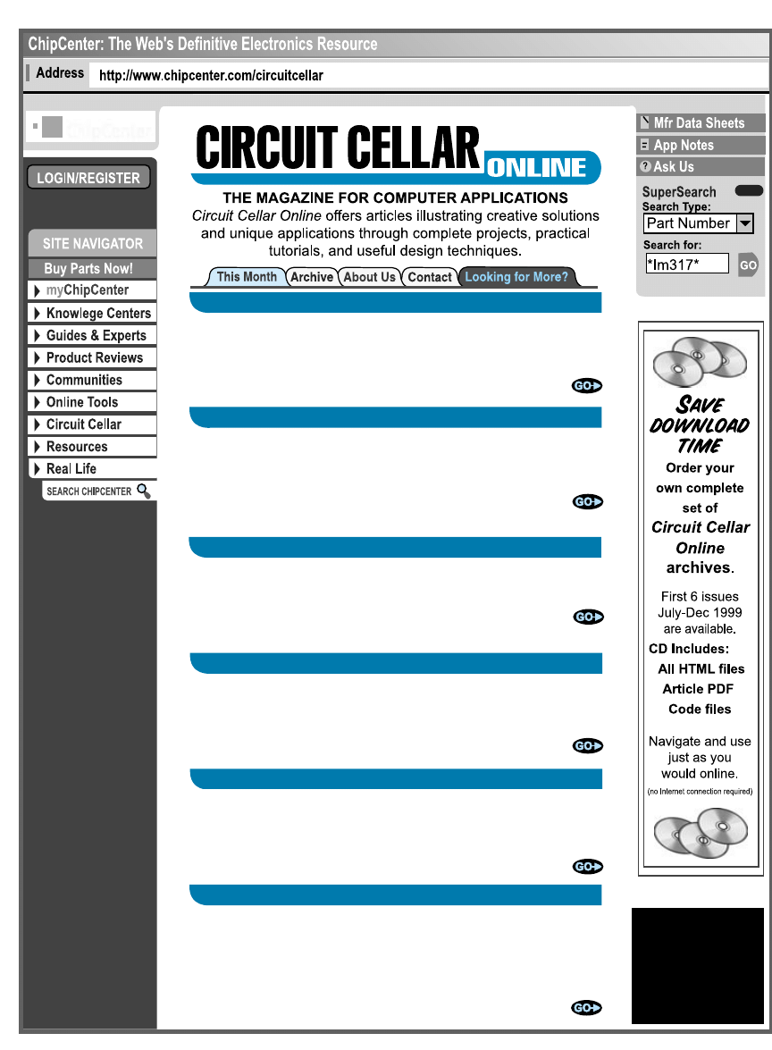
DESIGNING WITH THE MMC2107
by David Gonzales
Isn't the goal always to design a complex system using a minimum amount of com-
ponents? This month David discusses the key elements of a general-purpose micro-
controller and their use in a real-time application. The peripheral and processor inter-
action is essential for collecting, processing, and outputting data and, subse-
quently, you can't fully appreciate this interaction without a review of the
microcontroller functions. That's just the beginning.
April 2001
AN HC11 FILE MANAGER
Part 1: Laying the Foundation
by Walter Krawec
The best place to start following this series is at the beginning, when the foundation
is poured. Building this project from the ground up, Walter takes us through the first
part of using an HC11 file manager and shows us how to store multiple pro-
grams without having to memorize the addresses. Remembering all the
addresses is better left to HC11 than the human mind's memory. Then you
can let your mind wander to make your own project a success story.
April 2001
A SIMPLE ADC ON AN LTC1286 CHIP
by Yury Magda
Yury's been using the LTC1286 and now he wants to pass his knowledge on to
Circuit Cellar readers. The analog-to-digital converter circuit designed on the popular
low-cost chip has proved its benefits, like allowing the measurement of an
input voltage in electronic circuits and consuming a low supply current equal
to only 250 µA. Yury's circuit is straightforward, so get ready to easily soak up
the design and details.
April 2001
AN S-7800A/PIC16F877 JOURNEY
Part 4: Road Testing
by Fred Eady
Using his signature music analogies, Fred explores practical extraction or report lan-
guage, also known as Perl. Just as Janis Joplin grew in popularity, so has been the
journey of Perl, with its talent for encoding messages. We've gone from web
services to the post office and it's always good to end a series with a little
music. Cue the final song.
April 2001
STRUCTURED DESIGN
Part 2: Putting Theory into Practice
Lessons from the Trenches— by George Martin
Revisiting a former project by Jeff Bachiochi, George continues with his use of Nassi
Schneiderman flowcharts to develop a structured, manageable design. George origi-
nally intended to include case and switch constructs, so he picks up with that this
month. So, allow him to put this structured vehicle in reverse and back things
up a bit. The end of the road holds the tool to help isolate problems..
April 2001
DESIGNCON FUSION
Silicon Update Online— by Tom Cantrell
Variety is the spice of life. This month, Tom takes us on a tour of DesignCon 2001
and shows us the way the medley of players is responding to the winds of change.
As usual, there's great potential for what Tom describes as a high "neato factor," you
just have to run with the times, or you run the risk of being left behind.
April 2001
RESOURCES
•Portable MP3
Players
Rick Prescott
•Oscilloscopes
•Ethernet Cabling
Brant Schroeder
ASK
US
THE ENGINEERS
TECH-HELP
RESOURCE
Let us help keep your
project on track or simpli-
fy your design decision.
Put your tough technical
questions to the ASK US
team.
The Ask Us research
staff of engineers has
been assembled to share
expertise with others.
The forum is a place
where engineers can
congregate to get some
tough questions
answered, or just browse
through the archived
Q&As to broaden their
own intelligence base.
★★★★★★★★★★
Test Your EQ
8 Additional Questions

CIRCUIT CELLAR
®
www.circuitcellar.com
6
Issue 130 May 2001
EDITORIAL DIRECTOR/PUBLISHER
Steve Ciarcia
MANAGING EDITOR
Rob Walker
TECHNICAL EDITORS
Jennifer Belmonte
Rachel Hill
Jennifer Huber
WEST COAST EDITOR
Tom Cantrell
CONTRIBUTING EDITORS
Mike Baptiste
Ingo Cyliax
Fred Eady
George Martin
George Novacek
NEW PRODUCTS EDITOR
Rick Prescott
PROJECT EDITORS
Steve Bedford
Bob Paddock
James Soussounis
David Tweed
ADVERTISING
ADVERTISING SALES MANAGER
Kevin Dows
Fax: (860) 871-0411
(860) 872-3064
E-mail: kevin.dows@circuitcellar.com
ADVERTISING SALES REPRESENTATIVE
Elyshia Gottier
Fax: (860) 871-0411
(860) 875-2199
E-mail: elyshia.gottier@circuitcellar.com
ADVERTISING COORDINATOR
Valerie Luster
Fax: (860) 871-0411
(860) 875-2199
E-mail: val.luster@circuitcellar.com
ADVERTISING CLERK
Sally Collins
CONTACTING CIRCUIT CELLAR
SUBSCRIPTIONS:
INFORMATION: www.circuitcellar.com or subscribe@circuitcellar.com
To Subscribe: (800) 269-6301, www.circuitcellar.com/subscribe.htm, or
subscribe@circuitcellar.com
PROBLEMS: subscribe@circuitcellar.com
GENERAL INFORMATION:
TELEPHONE: (860) 875-2199 Fax: (860) 871-0411
INTERNET: info@circuitcellar.com, editor@circuitcellar.com, or www.circuitcellar.com
EDITORIAL OFFICES: Editor, Circuit Cellar, 4 Park St., Vernon, CT 06066
NEW PRODUCTS: New Products, Circuit Cellar, 4 Park St., Vernon, CT 06066
newproducts@circuitcellar.com
AUTHOR CONTACT:
E-MAIL: Author addresses (when available) included at the end of each article.
CIRCUIT CELLAR®, THE MAGAZINE FOR COMPUTER APPLICATIONS (ISSN 1528-0608) and Circuit Cellar Online are published
monthly by Circuit Cellar Incorporated, 4 Park Street, Suite 20, Vernon, CT 06066 (860) 875-2751. Periodical rates paid at Vernon, CT
and additional offices.
One-year (12 issues) subscription rate USA and possessions $21.95, Canada/Mexico $31.95, all other
countries $49.95. Two-year (24 issues) subscription rate USA and possessions $39.95, Canada/Mexico $55, all other countries
$85.
All subscription orders payable in U.S. funds only via VISA, MasterCard, international postal money order, or check drawn on U.S.
bank.
Direct subscription orders and subscription-related questions to Circuit Cellar Subscriptions, P.O. Box 5650, Hanover, NH
03755-5650 or call (800) 269-6301.
Postmaster:
Send address changes to Circuit Cellar, Circulation Dept., P.O. Box 5650, Hanover, NH 03755-5650.
For information on authorized reprints of articles,
contact Jeannette Ciarcia (860) 875-2199 or e-mail jciarcia@circuitcellar.com.
Circuit Cellar® makes no warranties and assumes no responsibility or liability of any kind for errors in these programs or sche matics or for the con-
sequences of any such errors. Furthermore, because of possible variation in the quality and condition of materials and workmanship of reader-
assembled projects, Circuit Cellar® disclaims any responsibility for the safe and proper function of reader-assembled projects based upon or from
plans, descriptions, or information published by Circuit Cellar®.
The information provided by Circuit Cellar® is for educational purposes. Circuit Cellar® makes no claims or warrants that reade rs have a right to
build things based upon these ideas under patent or other relevant intellectual property law in their jurisdiction, or that readers have a right to con-
struct or operate any of the devices described herein under the relevant patent or other intellectual property law of the reader’s jurisdiction. The
reader assumes any risk of infringement liability for constructing or operating such devices.
Entire contents copyright © 2001 by Circuit Cellar Incorporated. All rights reserved. Circuit Cellar and Circuit Cellar INK are registered trademarks of
Circuit Cellar Inc. Reproduction of this publication in whole or in part without written consent from Circuit Cellar Inc. is prohibited.
ASSOCIATE PUBLISHER
Joyce Keil
CHIEF FINANCIAL OFFICER
Jeannette Ciarcia
CUSTOMER SERVICE
Elaine Johnston
ART DIRECTOR
KC Prescott
GRAPHIC DESIGNERS
Naomi Hoeger
Mary Turek
STAFF ENGINEERS
Jeff Bachiochi
John Gorsky
QUIZ COORDINATORS
David Tweed
Michael Smith
EDITORIAL ADVISORY BOARD
Ingo Cyliax
Norman Jackson
David Prutchi
TASK
MANAGER
picture may be worth a thousand words, but
never underestimate the power of a few words—
especially when they’re the wrong words. Recently I
purchased an item that boasted “Quick and easy installa-
tion.” There was a half sheet of diagrams and four bulleted sections of
directions below that. It looked quick and easy. The first bullet under the
“Mounting” section said, “We recommend that you purchase the mounting
kit…” That’s funny, the box didn’t say anything about needing a mounting
kit, nor were there any mounting kits in close proximity on the shelf when I
purchased the item. After looking at the components for a few minutes, I
decided that I could duplicate the mounting kit with spare parts.
Bullet number one under the “Wiring” section noted that the model I had
purchased may require the additional wiring harness kit. The wiring situation
would take more time to workaround than I had scheduled for the entire
project, so I caved and decided to go back to the store in search of the
wiring kit. But not before reading the rest of the directions to see what else I
actually needed. (The only section that didn’t suggest additional purchases
was “Disposal of damaged units.” Go figure.)
After I got the necessary parts, installing the unit really was quick and
easy. But the ease of installation was not satisfying enough to forget my
frustration at the outset. I’m sure the confusing language on the box was
not intentional (if the box listed the suggested “accessories” I probably
would have purchased them originally), but it makes me wonder about a
company that doesn’t look at things through the customer’s eyes.
A couple of months ago, our foreign subscribers received a letter about
the new electronic edition of
Circuit Cellar. Judging by your responses and
after looking at the letter again, it’s clear that the letter was somewhat con-
fusing. I apologize for the confusion and would like to clarify a few things
about the electronic edition of
Circuit Cellar for all of our readers.
First of all, the print magazine is not being replaced by the electronic edi-
tion and all foreign subscribers do not have to subscribe to the electronic
edition. The electronic edition is simply a new option that can benefit foreign
subscribers (no extra mailing costs and no shipping delays).
Next, a subscription to the electronic edition is not included with your print
magazine subscription. A one-year subscription to the electronic edition
costs $15 (USD), regardless of your geographic location.
And last, subscribing to the print magazine and subscribing to the elec-
tronic edition are two unrelated processes. You can subscribe to both simul-
taneously, but because electronic subscriptions and print subscriptions are
managed separately, there is not a way (at this time) to convert your sub-
scription from one form to the other. To subscribe to both formats, you need
to fill out both sets of subscription forms.
For more information, stop by our homepage and click on Electronic
Edition. There you’ll find a section of FAQ, as well as instructions for down-
loading a sample issue. If you have any questions about the electronic edi-
tion of
Circuit Cellar, feel free to e-mail us at eeinfo@circuitcellar.com.
Thank you for your patience and understanding as we work to enhance
the products and services that
Circuit Cellar provides.
rob.walker@circuitcellar.com
Cover photograph Ron Meadows—Meadows Marketing
PRINTED IN THE UNITED STATES
a
Clear as Mud
UL Class I, Group D for atmospheres with acetone,
ammonia, benzene, butane, cyclopropane, ethanol, gaso-
line, hexane, methanol, methane, natural gas, naphtha,
and propane; Class II, Groups E, F, and G for combustible
metal dusts, including aluminum, magnesium, and their
commercial alloys, and atmospheres containing com-
bustible carbonaceous dusts.
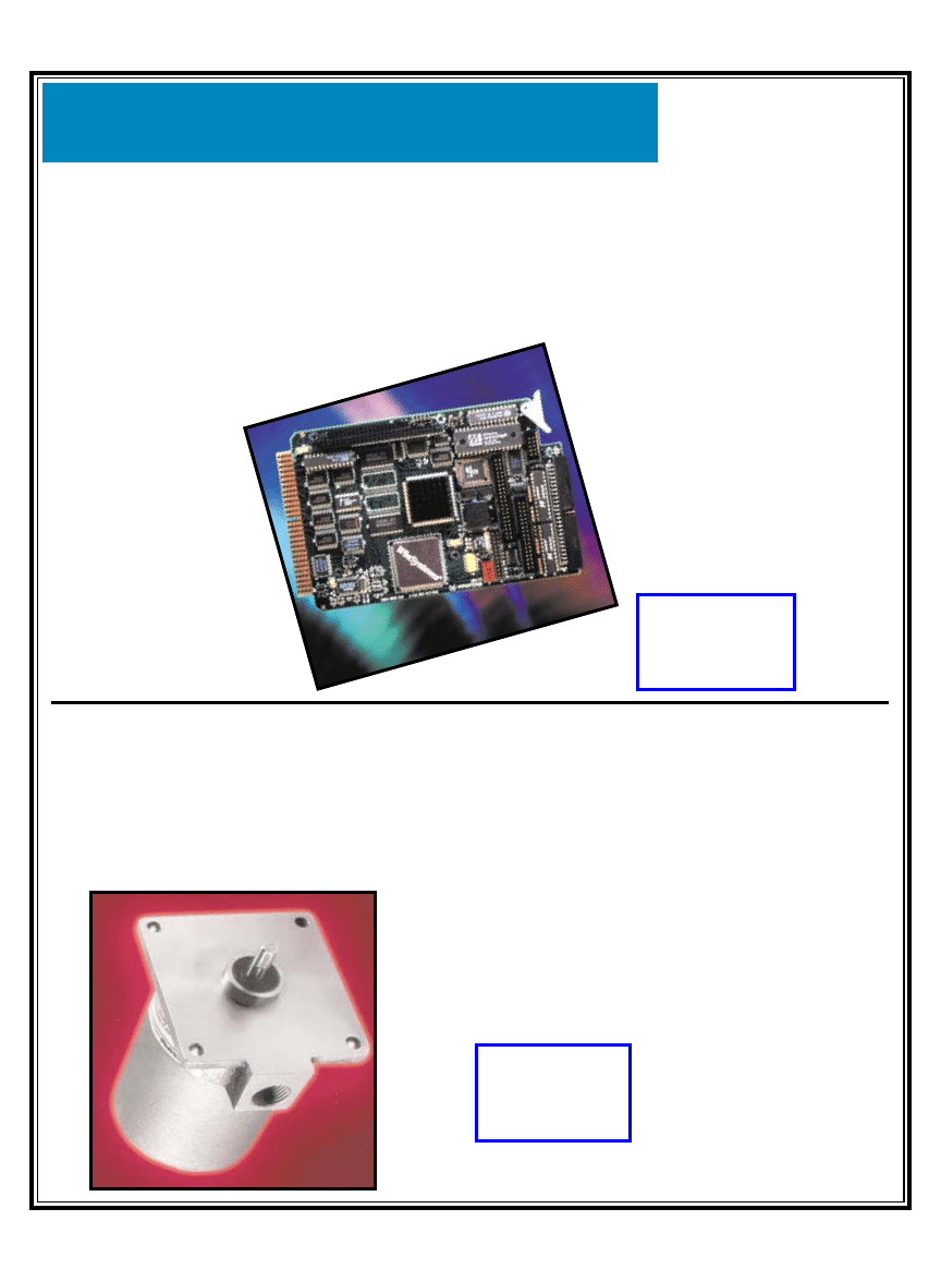
The encoders are rugged, high-performance, incremental
optical devices that feature an environmentally sealed,
cast aluminum housing. A stainless steel shaft and clear
anodized housing provide corrosion resistance. Electrical
outputs are electronically compatible with almost all
drives and PLCs. Differential line driver outputs are avail-
able for long cable runs and higher noise immunity.
The encoders sell for $750.
Danaher Controls
(847) 662-2666
Fax: (847) 662-6633
www.dancon.com
NEWS
8
Issue 130 May 2001
CIRCUIT CELLAR
®
www.circuitcellar.com
NEW PRODUCT
NEW PRODUCT
Edited by Rick Prescott
HAZARDOUS ENVIRONMENT ENCODER
Series X25 encoders are a new generation of hazardous
duty rotary encoders that are ideal for use in speed-feed-
back, cut-to-length measurement, and positioning applica-
tions in corrosive and/or explosive atmospheres. Encoders
are designed for use in environments such as UL Class I,
Group C for atmospheres such as ethyl ether and ethylene;
STD BUS CPU
The MCM-DXS is a high-integration STD bus CPU.
The CPU is a mid-ranged product based on the AMD 586
processor. This board is targeted for embedded applica-
tions including medical, transportation, test and instru-
mentation equipment, telecommunications, and machine
control.
Compatible with the x86-class of CPUs, the
CPU runs a vast amount of software
tools, utilities, and operat-
ing systems. The AMD
586 CPU also includes
a 16-KB cache and float-
ing-point processor for
math-intensive applica-
tions. The board is popu-
lated with 4 to 32 MB of
surface-mounted DRAM.
The DRAM is soldered
directly to the printed circuit
board to improve reliability for
applications subject to shock
and vibration. The CPU can
operate as a standalone SBC or
you can add off-the-shelf or user-designed IEEE 96 I STD
bus or PC/104 expansion UO modules to match the exact
application. These two expansion methods allow your
hardware solution to conform to open standard architec-
tures without having to pay for expensive pro-
prietary solutions.
The board integrates the basic AT peripher-
al complement including the keyboard con-
troller, 16-channel interrupt controller, and
real-time clock. Onboard peripherals are
mapped in the same location as a PC-AT,
including seven DMA controllers, three
16-bit counter/timers, two interrupt con-
trollers, keyboard controller, speaker
port, and battery-backed real-time
clock.
The price, which includes 4 MB of
DRAM memory is $795.
www.circuitcellar.com
CIRCUIT CELLAR
®
Issue 130 May 2001
9
NEW PRODUCT
NEWS
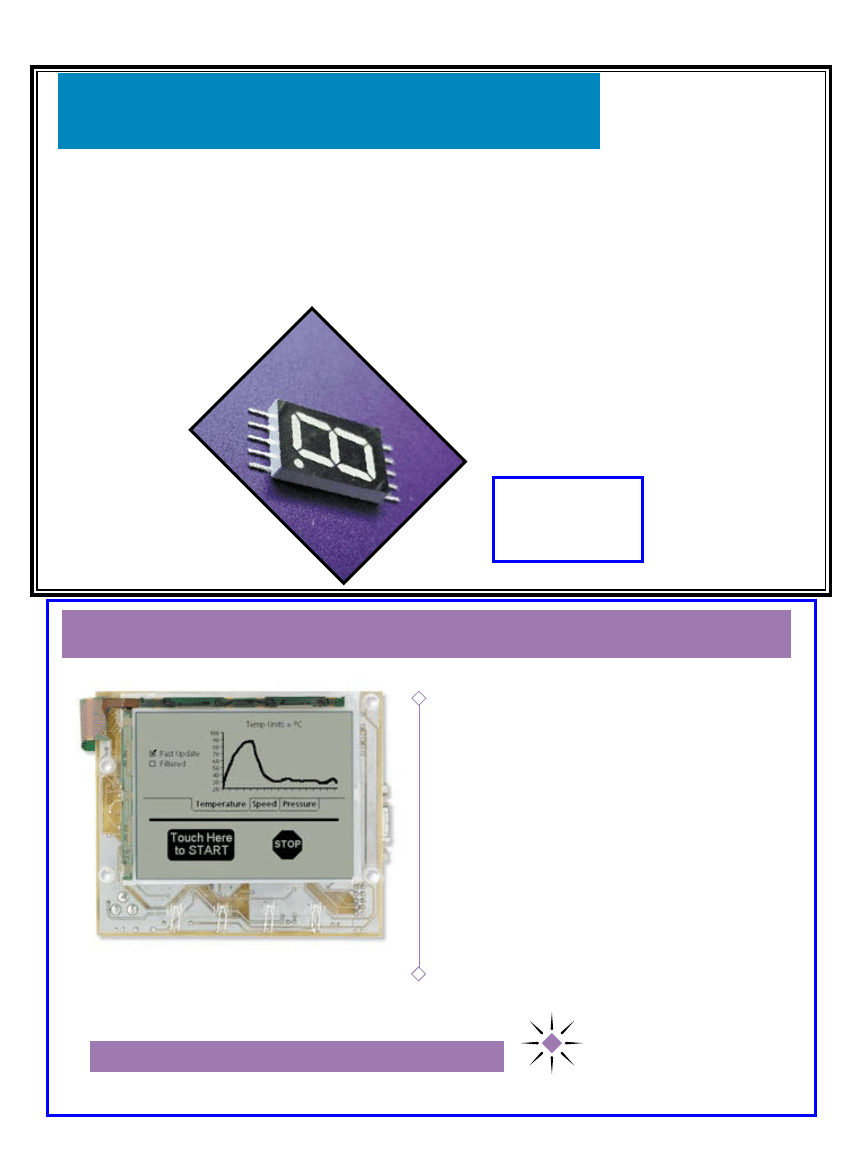
SURFACE-MOUNTABLE LED DISPLAY
This LED display is the world’s first 7-segment numer-
ic surface-mountable display. This device makes it possi-
ble for design and construction of equipment and instru-
mentation with numeric LED readouts on surface-mount
technology (SMT) boards and manu-
facturing processes. The LED dis-
play is ideal for a wide range of
applications including
timers, controllers, coun-
ters, test equipment,
or virtually any
system requiring
a numeric dis-
play where sur-
face-mount technolo-
gy is mandated by the
overall design and cost
parameters.
This display is based on a low-
profile, insert molded flat lead
frame package which stands just 3.3 mm (0.130
″
) off the
surface of the circuit board. The package measures 19
mm (0.748
″
) high × 12.7 mm (0.500
″
) wide, with a 14.22-
mm (0.56
″
) high numeric character. Each of the seven
segments is individually-addressable to create all digits
from zero through nine, plus several additional charac-
ters. A trailing decimal point is also included. Standard
color choices include state-of-the-art GaP green (565 nm)
and GaAsP high-intensity red (635 nm), with optional
blue and yellow available. Light output levels are as high
as 3200 MCD with a forward current of 10 mA. Units
can be ordered with a choice of common cathode or
common anode configurations.
The cost is $0.82 each in quantities of 1000.
Lumex, Inc.
(800) 278-5666
Fax: (800) 944-2790
www.lumex.com
– create a GUI in hours/days instead
– converts from HTML, JPEG, and GIF
into small, quickly-executable Amulet µHTML
1/4 VGA, 3.8-inch, Monochrome Display
bright backlight and fully-integrated analog touch panel
– manages the GUI, interacts with
the user, and controls the LCD – Frees up your micro!
– easily interfaces to most micro-
controllers (8/16/32-bit and even DSPs)
Replaces Traditional GUI Library
complex GUI programming, or RTOS required
– Up to 115.2 Kbps, cable included
64K-Bytes of Onboard Flash Memory
hundreds of Amulet µHTML pages that you create
Starter kit (STK-GT320) also includes our
Compiler, sample HTML files, and sample images.
Ready To Integrate Into Your Product
www.AmuletTechnologies.com (408) 244-0363
©2001 Easy GUI and µHTML are Trademarks of Amulet Technologies. U.S. and Foreign Patents Pending.
10
Issue 130 May 2001
CIRCUIT CELLAR
®
www.circuitcellar.com
ost of the com-
plexity of today’s
vehicles results from
requirements for cleaner,
more efficient engines. These engines
are controlled by algorithms and look-
up tables, which ensure that the
engine is running optimally. Sensors
carefully measure crank position, air
temperature and pressure, and throttle
position. Microcontrollers such as
Motorola’s MPC565 then are used to
examine the output of the sensors and
use the data to manage the engine.
In this arti-
cle, I will
explore signal
measurement
and sensing
using Motorola’s
MPC565.
Designed for
powertrain con-
trol, the
MPC565 is one
of the largest
microcontrollers
on the market
today, with 14
million transis-
tors and 1 MB of
internal flash
memory.
There’s no question
that the automotive
industry has benefit-
ted from the growth
and development of
the microcontroller.
Engine control is one
of the main automo-
tive applications for
today’s micros, so
Andrew shows us
how controllers like
the MPC565 do it.
The modular I/O system (MIOS) is
capable of input capture, pulse width,
and period measurement. To illustrate
the use of the MIOS for signal meas-
urement, I’ll show you how to gener-
ate and vary the frequency and pulse
width of a waveform and then meas-
ure the period and duty cycle of the
signal using the dual-action sub-mod-
ule (MDASM).
THE MIOS
The MDASM can take pulse width
and period measurements and also
perform input capture on 10 channels.
You’re going to use the MDASM to
measure the period and pulse width of
a waveform that you’ll generate using
the PWM sub-module. You’ll also
capture the waveform using the Input
Capture mode. These three measure-
ment and sensing tools allow the
MPC565 to sense input waveforms
and demodulate PWM to gather infor-
mation for further processing using
the PowerPC microprocessor core.
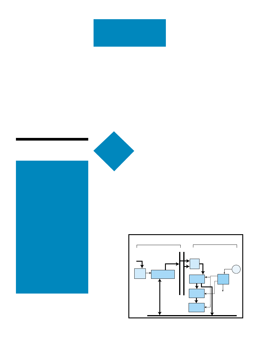
Figure 1 shows the MDASM. It has
three data registers that are accessible
to the software from the various
modes. For some of the modes, two of
the registers are cascaded together to
provide double buffering. The value in
one register automatically transfers to
another register at the correct time so
that the minimum pulse is just one
16-bit count.
To measure the width of an input
pulse, the MDASM has two capture
registers so that only one interrupt is
Andrew Lillie
Measurement and
Sensing with the MPC565
m
MIOS Modulus counter sub-module
From
prescaler
or pin
Clock
select
16-bit Up-counter
Bus
select
16-bit
Register A
16-bit
Register B1
16-bit
Register B2
Edge
detect
Input
pin
Input
capture
interrupt
on
designated
edge
Up to four
16-bit
counter
buses
MIOS Double-action sub-module
in IPM mode (MOD3 to MOD0 = 0b0010)
Sub-module bus
Figure 1—
The MDASM block diagram shows the function of the three result registers
and the modulus counter.
FEATURE
ARTICLE

www.circuitcellar.com
CIRCUIT CELLAR
®
Issue 130 May 2001
11
interested only in the latest period
measurement, one 32-bit coherent
read instruction can get both the cur-
rent and previous samples.
A configurable PWM module is
within the MIOS, allowing you to
adjust the frequency from 10 MHz to
less than 1 Hz and the duty cycle
from 0 to 100% with a variable degree
of resolution.
Now, you’re ready to experiment
using the MDASM. So, it’s time to
generate a waveform using the PWM.
GENERATING TEST SIGNALS
The MPC565 MIOS has 12 chan-
nels that can be used as pulse width
modulators. You’ll use channel 0.
Each PWM channel is controlled by
one system register and four registers
specific to that channel.
In order to use the PWM channels,
first you need to start the MIOS
counter. By default, the inter-module
bus (IMB) clock is half of the system
clock, but for this case, set it at
40 MHz to maximize the resolution
at a given frequency of the generated
needed after the second edge.
The software can read both
edge samples and subtract
them to get the pulse width.
The leading edge sample is
double latched so that the
software has the time of one
full period of the input signal
to read the samples to be
sure that nothing is lost.
A modulus counter sub-
module serves as the time-
base for the MDASM config-
ured in the Input Pulse
Width Measurement mode.
When the leading edge (programmed
to be rising or falling) of the input sig-
nal occurs, the state of the 16-bit
counter bus is saved in data register
B1. When the trailing edge occurs, the
counter bus is latched into data regis-
ter A and the content of register B1 is
transferred to register B2.
This operation leaves register B1
free for the next leading edge, which
occurs as soon as the next clock
cycle. When enabled, an interrupt is
provided after the trailing edge to
notify the software that PWM data is
available for a new pulse. After the
trailing edge, the software has one
cycle time of the input signal to
obtain the values for each edge.
Two samples are also available from
a MDASM sub-module for period
measurement. The software can read
and subtract the previous and current
edge counter values. As with pulse
width measurement, the software
avoids missing samples by ensuring
that the interrupt response time is
faster than the fastest input period.
Alternatively, when the software is
waveforms.
The MIOS counter
prescaler sub-module
(MCPSM) divides the sys-
tem IMB clock to generate
the counter clock. It is
designed to synchronize all
of the sub-modules with
the same division of the
main clock. The clock sig-
nal is prescaled by loading
the value of the clock
prescaler register into the
prescaler counter every time
it overflows. This allows all
prescaling factors between 2 and 16.
Counting is enabled by asserting the
PREN bit in the control register.
The PWM uses one count of the
MIOS counter per transition (rise and
fall) of the PWM signal; therefore, the
maximum frequency that the PWM
can generate is half of the MIOS
counter clock, even if the PWM chan-
nel divider is set to 1.
The status/control register controls
the MCPSM. Set bit 1 high to enable
the counter and write 0010 to bits 12
to 15 to set the divider to 2 for the
fastest counter possible. The faster
the counter, the faster the waveforms
you can produce and the greater the
resolution of the waveform definition.
Write 0x8002 to register 0x306816
(MCPSMCR). If you want to know
more details about the MIOS register
definitions, consult the MPC565
User’s Manual
. [1]
PULSE GENERATION
With the MIOS counter pro-
grammed to 20 MHz, the next step is
to program the PWM channel. The
PWM period register sets the number
of divisions per period of the wave-
form (i.e., resolution of a single peri-
od). Special consideration must be
taken when choosing the resolution
of the wave to be produced because it
involves a compromise. The resolu-
tion of the wave is inversely propor-
tional to the maximum frequency
that can be produced. Higher resolu-
tion requires more cycles of the refer-
ence clock per period and therefore a
lower overall frequency.
The period register contains a bina-
ry value corresponding to the number
Table 1—
Prescaler bits in the MPWMSCR and MMCSM set clock divider ratios.
Prescaler value (CP7…CP0 hex)
MIOS14 Prescaler clock divided by:
FF
1
FE
2
FD
3
FC
4
FB
5
FA
6
F9
7
F8
8
…
…
02
254 (2
8
– 2)
01
255 (2
8
– 1)
00
256 (2
8
)
Bit(s)
Name
Description
0
PINC
Clock input pin status bit
1
PINL
Modulus load input pin status bit
2
FREN
Freeze enable
3
EDGN
Modulus load falling-edge sensitivity
4
EDGP
Modulus load rising-edge sensitivity
5 and 6
CLS1 and CLS0
These read/write control bits select the clock source for the modulus counter.
7
Reserved
8 to 15
CP7 to CP0
This 8-bit read/write data register stores the modulus value for loading into
the built-in 8-bit clock prescaler. The new value is loaded into the prescaler
counter during the next counter overflow or when setting bits CLS1 and
CLS0 for selecting the clock prescaler as the clock source. Table 1 gives
the clock divide ratio according to the CP7… CP0 values.
Table 2—
The MMCSM configures the modulus counter to provide a reference clock to the MDASM by which
events are recorded.
12
Issue 130 May 2001
CIRCUIT CELLAR
®
www.circuitcellar.com
of MIOS clocks allocated to the period
of the waveform. Program PWM chan-
nel 0 with a period resolution of 20
divisions. Write 0x0014 to address
0x306010. This results in each period
being divided into 20 50-ns ticks, pro-
ducing a 1-MHz waveform.
The PWM pulse register sets the
number (binary) of divisions, or ticks,
from the period register (above) that
are high. This means that the ratio of
the pulse register to the period regis-
ter determines the duty cycle of the
produced signal. The value in the
pulse register must be less than the
value in the period register. Begin by
programming channel 0 with a 50%
duty cycle (or 10, with a period of 20)
by writing 0x000A to 0x306002. Vary
the period resolution and pulse width
parameters when experimenting with
the MDASM measurement modes.
The last eight bits of the PWM sta-
tus/control register (MPWMSCR) set
the clock divider for the particular
PWM channel. This divider operates
on the MIOS clock whose frequency
you set earlier. Each PWM channel
can use a divisor to slow the MIOS
counter clock.
If the IMB is operating at 40 MHz
and you divide that by two to get a
MIOS counter at 20 MHz, then set-
ting channel 0 to divide the MIOS
counter by one provides 1 MHz at a
resolution of 20. Table 1 shows the
eight-clock prescaler bits for the
MPWMSCR. Load 0x54ff into register
0x306006 to enable the output for
PWM with a divisor of one in
Transparent mode.
MEASURING SIGNALS
Now on to the good stuff! To meas-
ure the waveforms of the signal that
you generated earlier, connect the
PWM output on channel 0 to the
MDASM input on channel 11. This is
also a good time to connect an oscil-
loscope to verify the generated signal.
The MPC565 MIOS has a modulus
counter sub-module (MMCSM) that
can be configured as a 16-bit free-run-
ning counter to which events can be
referenced as they are detected by the
MDASM. The MDASM and MMCSM
work together to measure input wave-
forms. To begin,
set the counter to
be free-running
and automatical-
ly rollover when
it reaches its
maximum value.
Again, the
MMCSM status/
control register
controls the
counter. The last
eight bits of this
register are the
clock prescaler,
exactly like those
used earlier for
the PWM in
Table 1.
Set up the
MDASM to count
on rising edges (bits 3 to 4) and to use
the MMCSM internal clock bus. You
will set it up to follow the MMCSM
clock with a prescaler divisor of one.
This means that the counter will run
at 20 MHz, or 50 ns per count.
Following Table 2, configure the
MMCSM for a divisor of one (bits 8 to
15) and to use the MMCSM clock
prescaler (CLS1:0) and load on rising
edges (EDGP) by loading 0x0eff into
0x306036.
Internal clock synchronization
using the MMCSM allows a reference
clock up to half of the system fre-
quency. Alternatively, an external
clock can be applied for externally
synchronous measurement to a maxi-
mum frequency equal to one quarter
of the system frequency.
Bit(s)
Name
Description
0
PIN
Pin input status
1
WOR
In DIS, IPWM, IPM, and IC modes, the wired OR bit is not used.
2
FREN
The freeze enable bit is cleared by reset.
3
Reserved
4
EDPOL
In DIS mode, the polarity bit isn’t used. Reading it returns the last value written.
In IPWM mode, EDPOL selects the capture edge sensitivity of channels A and B.
1 = channel A captures on a falling edge. Channel B captures on a rising edge. 0 =
channel A captures on a rising edge. Channel B captures on a falling edge.
In IPM and IC modes, EDPOL selects the input capture edge sensitivity of
channel A. 1 = channel A captures on a falling edge. 0 = channel A captures on a rising edge.
5
FORCA
In DIS, IPWM, IPM, and IC modes, the force A bit isn’t used and writing to it has no effect.
6
FORCB
In DIS, IPWM, IPM, and IC modes, the force B bit isn’t used and writing to it has no effect.
7 and 8
Reserved
9 and 10
BSL1 and BSL0
The bus select bits select which of the four 16-bit counter buses is used by the MDASM.
Note that unconnected counter bus inputs are grounded.
11
Reserved
12 to 15
MOD3 to MOD0
The four mode select bits select the MDASM’s mode of operation (see Table 4).
To avoid spurious interrupts, I recommend disabling MDASM interrupts before changing the
operating mode.
Table 3—
The MDASM status/control registers can configure each of the 10 MDASM channels independently to allow different kinds of simulta-
neous measurements.
Mode selection; EDPOL = 0
Input signal
0×0500
0×1000
0×1100
0×1250
0×1525
0×16A0
A
A
Flag reset
by software
A
Flag reset
by software
16-bit
Counter bus
Flag bit
MDASMAR Captured value
0×××××
0×1000
0×1250
0×16A0
0×××××
0×××××
0×1000
0×××××
0×1250
0×1250
0×1000
0×16A0
B1 Value
B2 Value
Figure 2—
Input period measurement using the MDASM allows accurate frequency measurement. Note the use of
the flag bit.
www.circuitcellar.com
CIRCUIT CELLAR
®
Issue 130 May 2001
13
To ensure that the counter starts
properly, reset it by loading zeros into
the modulus latch, read/write register.
This register contains the 16-bit value
to be loaded into the MMCSM count-
er. Write zeros to 0x306032.
With the clock now running, you
can set up the MDASM to detect the
waveform periods and reference them
to this counter. In this case, you will
use only one of the 10 MDASM chan-
nels. All of the channels can be pro-
grammed the same way. Depending
on your application, you may want to
program one each for period measure-
ment, PWM, and input capture.
A control register configures each
MDASM channel, and results are
obtained from the two data registers.
The status/control register contains a
read-only bit reflecting the status of
the MDASM pin as well as read/write
bits related to its control and configu-
ration. The MDASM status/control
(MDASMSCR) register (address
0x30605E) will be used to initialize
MDASM channel 11 for your initial
measurements (see Table 3).
When programming the MDASM-
SCR, notice that bit 0 in Table 3 is a
read-only status bit that indicates the
state of the incoming waveform.
Because you don’t want the MDASM
to freeze in Background Debug mode,
bit 2 will be left as 0. Bit 4 will be 0
to trigger the MDASM counter on the
rising edge. Write 0 to bits 9 and 10
to select counter bus 0 as pro-
grammed in the modulus counter
sub-module. In order to perform fre-
quency measurement, you need to
measure the input period (MOD 0010
in Table 4). Load 0x0002 into the
MDASMSCR (0x30605E) to perform
input period measurement.
READING THE MDASM
When the MDASM detects a rising
edge, it will write the value of the
modulus counter to the data A regis-
ter. Upon detection of the following
rising edge (one period later) the
MDASM will move the first counter
value into data register B and write
the new value to register A. You pro-
grammed the counter to count at 50-
ns intervals. Subtracting register B
from register A sums the number of
counts during one complete period of
the input waveform.
Figure 2 illustrates the events in
the Period Measurement mode. Note
the operation of the flag bit as it trig-
gers the load of the counter value
into the data register. Using the –l
command ensures that the contents
of the two data registers are presented
simultaneously, so that you don’t
miscount because of the time it takes
to read the data out of memory on
two successive reads during Debug
(freeze) mode.
The BDM software returns eight
hex characters in one long word using
Mode selection; EDPOL= 1
Input signal
0×0500
0×100
0×1100
0×1250
0×1525
0×16A0
B
A
Flag reset
by software
Flag reset
by software
16-bit
Counter bus
Flag bit
MDASMAR Captured value
0×××××
0×1000
0×1100
0×1100
0×××××
0×××××
0×1000
0×××××
0×1000
0×1000
0×1000
0×1250
B1 Value
B2 Value
B
B
0×1525
0×1525
0×1250
0×1250
0×1000
0×16A0
A
Figure 4—
Pulse width measurement is the same as period measurement except that the falling edge triggers the
second bus counter read. This example shows negative pulse width measurement.
#> read -l 0×306058
(0×306058)
00306058
5020500C
00028002
.
.
.
.
.
.
.
.
.
Figure 3—
When you use the – l command, the BDM
software returns eight hex characters in one long
word.
14
Issue 130 May 2001
CIRCUIT CELLAR
®
www.circuitcellar.com
measurements, set the MOD[3:0] bits
to 0001 (see Table 4). This mode
allows the width of a positive or nega-
tive pulse to be determined by captur-
ing the leading edge of the pulse on
channel B and the trailing edge of the
pulse on channel A; successive cap-
tures are done on consecutive edges of
opposite polarity. The edge sensitivity
is selected by the EDPOL bit in the
MDASMSCR register.
After performing a long read of data
registers A and B again, you now have
the number of 50-ns counts that rep-
resents the length of the positive
pulse. Using the PWM pulse width
register, vary the width of the PWM
pulse by changing the number of posi-
tive 50-ns ticks. Set the waveform
resolution to 20 so there’s room to
play with when you experiment with
the Pulse Width Measurement mode.
For my 10% duty cycle signal (still at
1 MHz), I achieved the results dis-
played in Figure 5.
One more MDASM mode allows
you to capture the events of an
incoming waveform. The Input
Capture mode (ICM) can be useful for
communication circuits or timing cir-
the code shown in Figure 3. Don’t be
alarmed if your results are different
from these, because these values are
read from a free-running counter, and
the values constantly change. What
matters is the difference between the
two bytes of the word. Also remember
that the counter may pass zero and
restart during a measurement.
The long word 5020500C contains
the contents of the two data registers.
Data A contains 5020 and data B con-
tains 500C. When you subtract regis-
ter B from register A, you get 20 in
decimal. To calculate the frequency,
multiply by 50 ns and take the recip-
rocal to get 1 MHz. Using a similar
approach, you can measure the pulse
width of the waveforms (see Figure 4).
To reprogram the MDASM status
and control register for pulse width
Mode selection; EDPOL = 0
Input signal
0×0500
0×1000
0×1100
0×1250
0×1525
0×16A0
A
A
Flag reset
by software
Flag reset
by software
A
Flag reset
by software
16-bit
Counter bus
Flag bit
MDASMAR Captured value
0×××××
0×1000
0×1250
0×16A0
0×××××
0×××××
0×1000
0×××××
0×1250
0×1250
0×1000
0×16A0
B1 Value
B2 Value
Figure 6—
Input Capture mode triggers the flag to capture the transitions on the input waveform, allowing an accu-
rate representation of the applied waveform in memory.
SOURCE
MPC565
Motorola, Inc.
(847) 576-5000
Fax: (847) 576-5372
www.motorola.com
REFERENCE
[1] Motorola, Inc., MPC565 User’s
Manual
.
RESOURCE
A. Lillie and R. Dees, “Using the
MIOS on the MPC555 Evaluation
Board,” AN1778, 1998.
cuits where periods of inactivity
greater than a certain length may
indicate a new condition. This mode
is identical to the Input Period
Measurement mode (IPM), with the
exception that the flag line is activat-
ed at the occurrence of the first
detected edge of the selected polarity.
In this mode, the MDASM functions
as a standard input capture function.
In this case, the value latched in
channel B can be ignored. Using the
ICM of the MDASM, you can record
at what times the edges occur on the
waveform (see Figure 6).
The dual-action sub-module of the
MIOS provides 10 channels that can
be used for similar measurements and
are easily configurable. Using all three
of the measurement modes I have
explored on a single signal provides a
thorough analysis. You can measure
the period, pulse width, and capture
when the pulses occur on any signal,
even one that isn’t periodic.
The MIOS is becoming a common
feature on many Motorola microcon-
trollers and offers flexibility for pulse
generation and measurement. Since
working with the MIOS, I‘ve found
some great applications for these
measurement modes and I expect that
you will find many more.
I
Andrew Lillie works in the Advanced
Vehicle Systems Division at Motorola
and helped design the MPC565. He
can be reached at andrew.lillie@
motorola.com.
MODE[3:0]
Mode
Description of mode
0000
DIS
During Disabled mode, the input pin is high impedance. PIN gives the state of
the input pin.
0001
IPWM
The input pulse width measurement is captured on the leading and trailing edges
of an input pulse.
0010
IPM
The input period measurement is captured during two consecutive rising or falling
edges.
0011
IC
This mode captures the input when the designated edge is detected.
Table 4—
The three input measurement modes are programmed into the MDASMSCR. Each channel can operate
in a different measurement mode concurrently.
#> read -l 0×306058
(0×306058)
00306058
E06AE068
00088800
.
.
.
.
.
.
.
.
.
Figure 5—
Subtracting E068 from EO6A makes two
counts, or 100 ns. One-hundred ns out of 1 µs is 10%
at 1 MHz.
RF modules and your Data Links....
65 Southbridge St., Auburn, MA. 01501 • Tel: 508-798-5004 • Fax: 508-798-4782
sales@lemosint.com • www.lemosint.com
Radiometrix specializes in the design and manufacture of low power radio products which help you to
rapidly implement high-reliability, cable free data links.
16
Issue 130 May 2001
CIRCUIT CELLAR
®
www.circuitcellar.com
ome springtime,
do your thoughts
turn to mulching the
planter beds? Each year
the discussion between my wife and I
goes the same way.
“Are you going to order the mulch
today?”
“Well, I really don’t know how
much to order.”
“Why don’t you just order what you
did last time?”
“It’s been so long, I’ve forgotten.”
“Why don’t you just measure the
beds and figure it out?”
“They’re all so irregular it’s almost
impossible.”
And so on. In case you had difficul-
ty identifying the speakers in that dia-
log, associate all the question marks
with the wife and the lame answers
with the husband—me.
Being a dyed-in-the-wool technolo-
gist, I thought there must be an easier
way to figure out an answer to this
problem other than putting in more
concrete or blacktop. The answer
turned into the Yard-Stick. I started
with the basic measuring wheel that
measures distance by rolling a wheel
along the path. I added a compass to
indicate direction, then recorded the
data so I could later send it to a PC. In
the PC, the direction and distance
data can be used to plot the area or
measure it. I included an LCD to give
you some real-time feedback, a few
switches, and a buzzer, and presto, I
arrived at the answer to every land-
scaper’s and home handyman’s dream.
The Yard-Stick uses an 87LPC764
microprocessor to integrate a compass
module, two-line LCD display, I
2
C
EPROM memory, RS-232 interface,
switch closure from the rolling wheel,
push button to start and stop meas-
urements, and a buzzer. The buzzer
warns you when the memory is full.
Figure 1 illustrates the system.
The device mounts on a shaft with
a wheel on the other end. The wheel
has a switch that closes every 6
″
. The
LCD tells you how to operate the
device and provides real-time feed-
back of the distance recorded and the
direction the unit is pointed. The
Yard-Stick constantly reads and aver-
ages the compass data, and every 6
″
it
records the current compass heading.
You can map the outline of multi-
ple areas by pressing the Start/Stop
button. Each closure defines a new
section to record. These sections then
can be downloaded to a PC via the
standard serial port as a text file. The
FEATURE
ARTICLE
With gardening sea-
son approaching,
David needed a way
to find out just how
much space the
flower beds took up.
With a little help from
a Philips LPC micro-
controller, there was
still plenty of time to
measure the gardens
and order the mulch
before snowfall.
David Penrose
The Yard-Stick
c
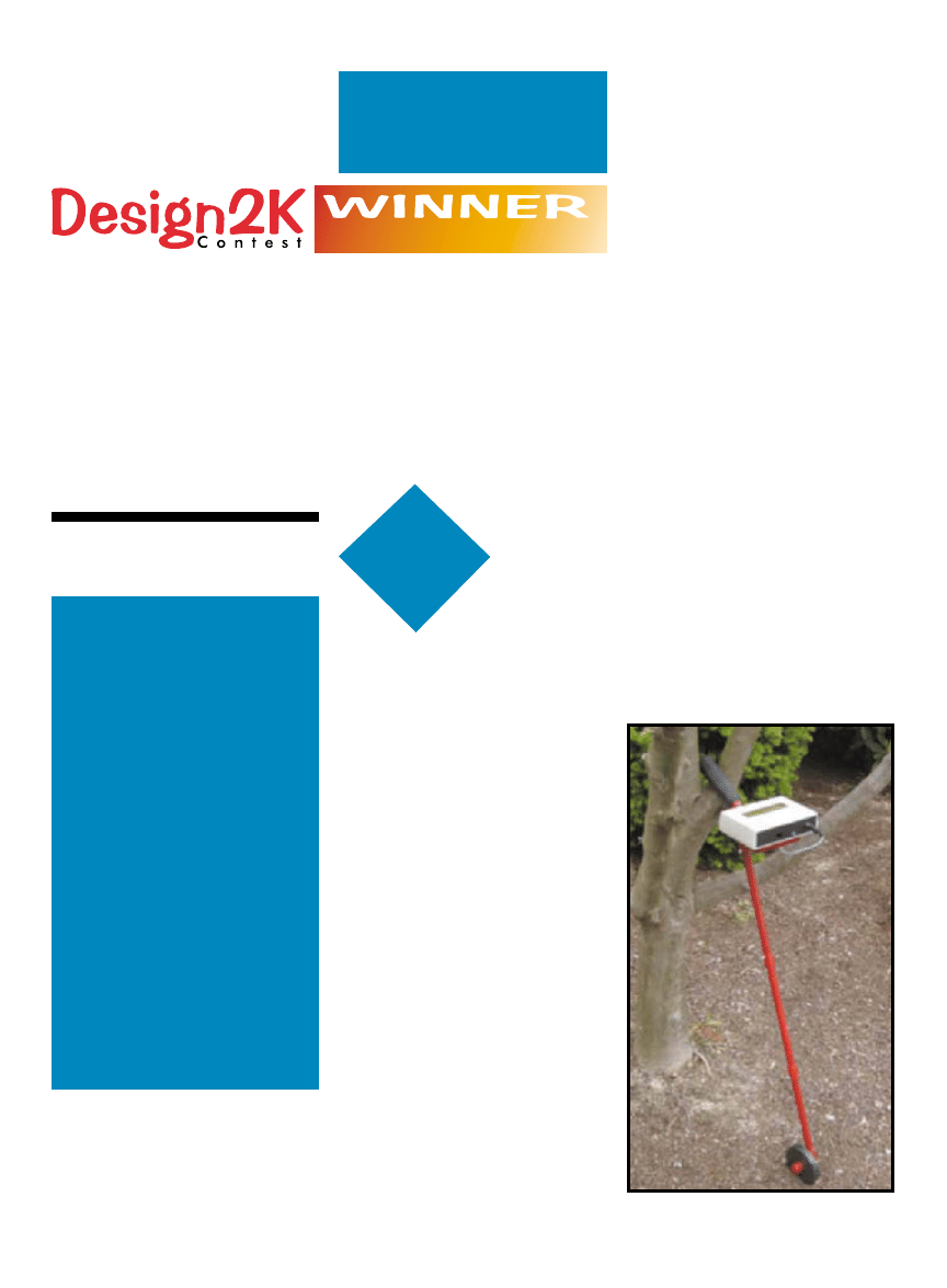
Photo 1—
Here’s the completed Yard-Stick.
www.circuitcellar.com
CIRCUIT CELLAR
®
Issue 130 May 2001
17
I
2
C EEPROM can record 4096 points
(two 8-bit words per point with 1° res-
olution); at 6
″
per point, that’s 2048
′
.
Section definitions are integrated with
the distance measurement; thus, they
don’t require additional storage. The
display is limited to 99.
The software was designed to make
the device simple and foolproof. You
can turn off power at any time and
not lose the data recorded. If the dis-
tances exceed 1800
′
, a display and
buzzer warn you that the memory is
filling up. You also are warned when
memory overflows, but at this point
the processor starts recording over the
oldest data. These features should
allow even the most avid gardener to
capture all the flowerbeds in one ses-
sion. Photo 1 shows the complete
unit with the measuring wheel,
frame, and electronic box.
Spring no longer carries the threat
of the unknown planter bed dimen-
sions. I am armed with the right tool
for the right job. But now spring has
passed, so I guess I have to wait until
next year to mulch. Once again tech-
nology comes to the rescue!
HARDWARE
The Yard-Stick uses a Vector 2X
compass. It is a two-axis, magneto-
inductive magnetometer that claims
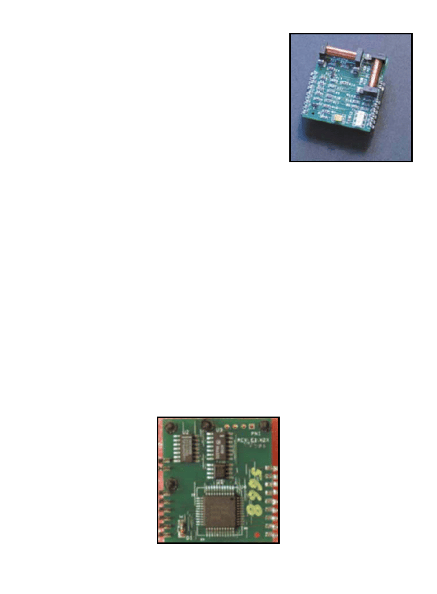
2° accuracy and 1° resolution. Photo 2
shows a top view of the unit and
Photo 3 shows a bottom view.
In Low Resolution mode, the com-
pass module is capable of five meas-
urements per second. The output is a
serial three-wire format compatible
with the SPI standard. The output for-
mat can be selected as binary coded
decimal (BCD) or binary output. This
project uses the latter. The Vector 2X
can be calibrated for “hard iron” devi-
ations, which means that it can be
mounted close to nonferrous metals
and the effect of these metals can be
calibrated out of the system’s output.
The Vector 2X can be operated in
Master or Slave mode. In Master
mode, it constantly outputs readings
following each internal calculation. In
Slave mode, a second device requests
a measurement and is notified when
the data is available. The processor
then must clock out 16 bits using the
clock line. Power for the Vector 2X is
standard TTL (5 V). Current draw in
Slave mode is about 4 mA when
polled at the 5-Hz rate and 100-µA
when idle. These power levels make
the unit attractive for a battery-pow-
ered device such as the Yard-Stick.
The Yard-Stick’s microprocessor is
the Philips 87LPC764, a 20-pin device
with 4 KB of onboard program memo-
ry and 128 bytes of RAM. The device
offers the option of disabling the
external reset and using an internal
reset, which frees one of the pins as
an additional input. I used this pin for
the end of conversion (EOC) signal
from the compass module to the
processor. If critical timing is not a
requirement for you, then an internal
oscillator can be selected, freeing the
two crystal pins as well.
In this application, the timing is
critical because the processor needs to
communicate using RS-232, so an
external crystal (11.0592) establishes
the clock frequency. The 87LPC764
has a high voltage tolerance allowing
for sloppy input supplies. Current
draw is about 5 mA when active, so
it’s an ideal device for a battery-pow-
ered application.
The processor includes the hard-
ware and firmware to support an I
2
C
bus that the Yard-Stick uses to com-
municate with an 8-KB EEPROM. If
you don’t use these pins for the I
2
C
feature, keep in mind that they are
open-drain outputs and must have a
pull-up to V
CC
to operate as outputs.
I’ve managed to forget these resis-
tors more than once and spent some
serious debug time chasing this trivial
mistake. The processor also has a
standard RS-232 serial port supported
by two pins (TxD and RxD). The
firmware behind this feature is stan-
dard with the ’8751 family and makes
serial communication a snap. In this
application, a MAX202 converts the
voltage on these pins to interface to
standard RS-232 levels using only the
5-V supply. The processor supports
two external interrupts, *INT0 and
*INT1 (*INT0 is shared with the SDA
pin on the I
2
C interface). The Yard-
Stick uses *INT1 to recognize switch
closure from the rolling wheel.
The processor has multiple timers
(Timer0, Timer1, watchdog, TimerI)
that are capable of supporting dedicat-
ed uses. Timer0 runs at about 8 ms to
establish a basic drumbeat to time
messages to you and debounce the
wheel and push-button switches.
Because I have faith in my software
(tongue is firmly in cheek) and upsets
can be cured with the off/on switch, I
didn’t use the watchdog timer.
Timer1I is capable of rescuing the
I
2
C bus from a hung condition. This
timer is tightly integrated with the
I
2
C hardware but still must be config-
ured for the approximate CPU clock
frequency and then enabled by the
software prior to the first I
2
C access.
After being enabled, it will interrupt
if activity on the bus ceases without a
stop condition being issued. The
interrupt logic should then try to free
the bus and reinitiate the processing.
The processor is also loaded with a
bunch of other features that allow you
Photo 2—
The X and Y sensor coils and the two rows
of connecting pins are on either side of the Vector 2X.
Photo 3—
The processing power is located underneath
the compass module.
18
Issue 130 May 2001
CIRCUIT CELLAR
®
www.circuitcellar.com
to compare voltage levels with
interrupts, detect brownout at
different power supply levels,
and so on. I see years of happy
experimentation with these
other features, but at some
point I decided to focus only on
the basics for the Yard-Stick.
NONVOLATILE STORAGE
Data storage is accomplished
using a 24C65 64-Kb serial EEP-
ROM. This chip is implement-
ed as 8192 8-bit words and is
designed to work with the I
2
C
bus. Multiple chips can be tied
to the I
2
C bus and addressed
separately using pins A0
through A2 on the 8-pin device. I
implemented only one chip at address
0 but included an extra socket just in
case the urge to grow hits me. The
chip has a pin that allows you to
write-protect the upper section of
memory in case the operating system
or some critical values need to be
stored in a secure space. The Yard-
Stick doesn’t use this and the words
are available for data storage.
The EEPROM’s limited number of
memory write cycles (1 million for
this device) isn’t a problem because
data is only written to the memory
when the wheel moves 6
″
. That
works out to be 500,000
′
, or 100 miles
for 1,000,000 cycles.
Each write takes about 10 to 15 ms.
A write can be up to 32 bytes, howev-
er, so speedup is offered by using this
page feature. The Yard-Stick writes
two words every time a meas-
urement is recorded, so you can
progress at the brisk pace of
50
′
/s (34 mph) without losing
data. The chip maintains data
without power so you can
measure an outside area, turn
off the Yard-Stick, go inside
and connect it to a PC, and
then download the data. When
powered up, the memory uses
less than 200 µA when active
and about 10 µA when inac-
tive.
The LCD is a standard 2 × 16
display with a low-voltage
backlight. I implemented the 4-
bit Communication mode to
conserve pins on the microprocessor
and have the clock share two of the
compass data pins. Contrast is con-
trolled by varying a positive supply to
pin 3 within about 600 mV. Some
higher performance units use a nega-
tive voltage to this pin, so check your
specifications. You can adjust this
voltage with a small potentiometer
that extends through the back of the
Yard-Stick.
As mentioned earlier, the RS-232
levels are converted by a MAX202
integrated circuit. This chip uses 0.1-
µF capacitors to generate the positive
and negative supply from the 5-V
input. These smaller capacitors make
a more compact arrangement and are
cheaper than the 1- or 10-µF caps used
by other units. The Yard-Stick uses
only one receiver and one transmitter
on this chip with no hardware flow
control implemented. This does not
create problems for the Yard-Stick’s
primarily one-way communication.
The only remaining hardware are a
low-voltage, low-power piezo buzzer,
an off/on switch, a push-button
switch with a pull-up resistor, and a
reed switch with a pull-up resistor for
the wheel switch. I placed 0.1-µF
capacitors between V
CC
and ground for
each chip and put a diode between
four AAA cells and the power to the
ICs. Then, the Yard-Stick was ready
for software.
SOFTWARE
The software is a simple polling
loop with two interrupt processes.
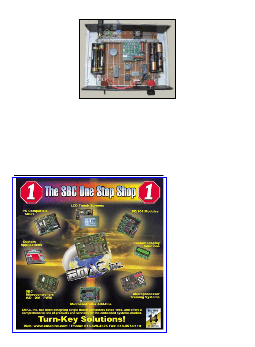
Photo 4—
The inside of the case shows the compass module mounted
with the processor, batteries, and auxiliary chips.

www.circuitcellar.com
CIRCUIT CELLAR
®
Issue 130 May 2001
19
The polling loop waits for you to push
the switch closure to change states or
for a serial character from a connected
PC to select some action. The device
begins from powerup by displaying
the sign-on message “Yard-Stick
V1.0”. It then enters a state waiting
for either a short button press to start
recording a section or a 2-s button
press to begin calibration. During the
waiting state, the Yard-Stick outputs
two messages to the display which
alternate at 2-s intervals.
The first message indicates the
device is waiting and you should press
Start to begin recording. The second
message indicates that a 2-s button
press will calibrate the unit. If the cal-
ibration action is selected, the next
message asks you to turn the unit
180° and press the button again. The
Vector 2X is placed in Calibration
mode by pulsing a pin on the device.
At the end of the calibration, the pin
is pulsed again and the compass cali-
brates its internal calculations.
Although you don’t have to cali-
brate, most people start recording ses-
sions with a calibration action
because it’s easy. Afterwards, the cali-
bration request message is suppressed.
Calibration can be done anytime the
unit is in-between sections by holding
down the button for 2 s.
When the device exits the waiting
state, it begins displaying a message
indicating the current heading both as
a compass point direction and numer-
ic degree. The distance traveled in a
direction is displayed on the same
line as the heading. The second line
of the display indicates the total dis-
tance traveled in the section. Each
time the compass direction changes
and the wheel records motion, the
distance at the current heading is
zeroed. The compass is read constant-
ly and a running average of four sam-
ples is calculated. The output of this
running average is displayed on the
LCD or recorded in memory.
Recording data in memory is trig-
gered by the wheel closure interrupt.
With each interrupt, the current com-
pass heading is recorded in memory
as two 8-bit words. The first word
contains the MSB of the integer value
and the second word contains the
LSB. Each time you
begin a new section,
the Yard-Stick records
one entry in memory
with the current head-
ing and bit 7 of the
first word set to indi-
cate the beginning of a
section.
Each wheel closure
interrupt then adds
entries to memory. If
you pause for 15 s, the
device will automatically write a stop
code (bit 6 of the first word) to the
last valid memory entry. If you con-
tinue moving, the stop code will be
removed as new entries are added.
This code ensures that if you shut
down without pressing the Start/Stop
button, a proper sequence will remain
in memory for the PC transfer. After
the stop code is added to memory, a
message asks you to press the
Stop/Start button to end the section.
The normal screen is displayed if the
unit begins moving again or after 2 s.
At the end of a section, the LCD
indicates the number of sections cur-
rently recorded and the total distance
traveled. This message is displayed for
2 s and then the “waiting for
start/stop button” message is dis-
played. These two messages alternate
until you press the button to begin a
new section or turn off the power.
If you exceed 90% of the 2048
′
capacity of memory, a low-memory
message is displayed and the piezo
buzzer is enabled. This continues for
5 s and then the normal display
returns. If the wheel is moving during
this time or if you press the button,
the normal actions will take place
because the wheel is processed during
an interrupt and the software is con-
stantly polling for a switch closure.
If recording continues past the
point of filling memory, an alarm
again will sound and the software will
record at location 0. Later, when data
is being dumped to a PC, this condi-
tion is recognized by a missing start
code in the first word of memory. All
memory is dumped to the PC to make
sure no data is lost. Normally only
data that is bracketed by a valid
start/stop code is dumped to memory,
but this overflow condition will prob-
ably disrupt these start/stop pairings.
The PC passing an “X” to the Yard-
Stick, indicating that an export of
data is desired, triggers dumping data
to a PC. The Yard-Stick responds by
putting out a message “Section x”,
indicating that the following data is
for the specified section (x). Then,
some lines of data will be output with
a three-digit number on each line
indicating the compass heading in
degrees. The format uses a carriage
return at the end of each line with no
line feed. The rate is 9600 bps with 8
bits, 1 start, 2 stop, and no parity bits.
At the end of the section, a message
“End x” will be output to indicate the
last data for the current section. If
more data is stored in memory, then
the next section will be output in the
same format. At the end of the export
process, the processor delays 10 s so
you can close the transfer operation.
After that, the processor reinitializes
itself. Data will remain unchanged in
memory; it changes only when you
press the Start/Stop button to begin a
new section.
Note that a number of other PC
actions are used to facilitate checkout
and maintenance. Any single charac-
ter code from the PC that is not rec-
ognized as one of these valid actions
will result in the display of a help
message. I did most of the unit check-
out using a hand-held terminal that
has a 4 × 20 display. One of the
actions codes (T) switches between
special positioning codes for this ter-
minal and the VT100 codes selected
for the standard PC display.
The Yard-Stick will display either
an “S-” or “H-” message indicating
which device it believes it is talking
Rolling
wheel
switch
Push-button
switch
2 × 16
LCD display
87LPC764
Microprocessor
Digital compass
module
8-KB EEPROM
memory
PC Connection
Figure 1—
This diagram of the Yard-Stick shows the major components.

20
Issue 130 May 2001
CIRCUIT CELLAR
®
www.circuitcellar.com
to. On-chip and I
2
C memory can be
read or written with the E and W
commands. The distinction between
these two memory spaces is made
when you enter either a two- or four-
character address. The former indi-
cates that the 128-byte on-chip mem-
ory is being addressed and the latter
indicates that all addresses are meant
for the I
2
C memory.
The processor can be restarted
using the F command to indicate that
a fresh start is desired. The averaging
of compass module samples can be
disabled by the A code. Each time the
A code is entered, the unit toggles
between averaging and no averaging.
The D command indicates that a
debug output is desired, and every
reading from the compass, the last
four samples, and the average value
are output to the display. This opera-
tion is toggled in the same fashion as
the A and T actions.
INTEGRATION
Photo 4 shows an internal view of
the electronic enclosure. The compass
module is a simple but demanding
device. My recommendation is to
read, reread, and read the spec sheet
again. The unit needs to be positioned
in the device with the pins labeled
P14–P11 pointing to the front, as is
shown in Figure 2.
The power-up sequence is also criti-
cal but easy. When power is applied,
the unit expects the Poll/Continuous
(*P/C), Calibrate (*CAL), Slave Select
(*SS), and Reset pins to be in a high
state. The *P/C, *CAL, *SS pins
weren’t a problem because they are
connected to the 87LPC764,
which I programmed to initial-
ize with high port pins. The
Reset pin must be left open to
make sure it goes high also.
Tying this pin to a 10-K
Ω
pull-
up resistor just confused the
unit because the voltage didn’t
rise as fast as the processor
pins. When confused, the
device plays dead.
This device is an interesting
mixture of an SPI interface and
control pins. The *SS input
selects the device for data read-
out and hence, floats serial
data out (SDO) and serial clock
(SCLK) when inactive. It doesn’t float
the calibration indicator (CI) nor end
of conversion (EOC) signals, however.
This means that pins need to be dedi-
cated on the processor to interface to
these signals.
I didn’t use the CI pin but did use
the EOC pin. I could have ignored the
EOC pin and replaced it with a soft-
ware delay that would allow for the
processing delay inside the compass,
but this gets ahead of the story.
Because *SS floats the SDO and
ignores the SCLK, I put these two sig-
nals on the same pins as two of the
data bits to the LCD display. The
LCD won’t read these pins until its
Enable (E) line is high, and the com-
pass won’t use them until the *SS
line is low, so everyone is happy if the
software cooperates. Cooperation
means leaving the shared SDO pin in
a high state when done with it (the
’51LPC issues a weak pullup in this
mode) so a read of the SDO can occur.
To use the device, the sequence
pulses the *P/C low for at least
10 ms. When this pin goes low, the
EOC pin will also drop low. After tak-
ing *P/C high, the software then
monitors the EOC line waiting for it
to return high (normally takes about
100 ms). After this line is high, the
software can select the device with
*SS low and begin clocking out 16
bits from SDO by pulsing SCLK (wait
5 ms prior to the first clock pulse).
The module allows pins *P/C and
*SS to be tied together with the only
penalty being that SDO and SCLK are
active when *P/C is pulsed low to
begin a conversion. This wasn’t a
problem in the Yard-Stick, so I saved
a pin by tying these two together.
With the low-to-high transition of
each clock, the SDO line returns a
data bit. Timing of these clock pulses
needs to be less than 1 MHz until the
last clock bit goes high, then the
processor has only 20 µs to read this
last data bit.
I turn off interrupts for this part of
the process to avoid problems. If the
*BCD/BIN pin is high or floating, this
data will be MSB to LSB of a 16-bit
integer indicating degrees. If you want
to use BCD instead, tie the *BCD/BIN
pin low and interpret the 16 bits as
BCD instead of the 16-bit integer.
The Resolution (*RES) pin selects a
high- or low-resolution internal pro-
cessing mode. The Yard-Stick uses the
latter. In Low-Resolution mode (pin
grounded), data is available at a 5-to
10-Hz rate. Pulling this pin high puts
the unit into High-Resolution mode,
which is recommended with areas of
weak magnetic force. In this mode,
samples are available at 2.5 to 5 Hz.
By the way, don’t mistake this pin for
the Reset pin.
If you want to do it yourself, note
that the compass has a Raw pin.
Grounding this pin results in the unit
returning 32 bits of raw X and Y sen-
sor data. You can then calculate head-
ing or magnetometer readings using
equations that are supplied with the
spec sheet. The advantage here is that
you can do your own calibration and
preserve this in software. The com-
pass module loses its calibration
information when power is removed.
The disadvantage is that there is an
ungainly amount of calculations
involved with bunches of sines,
cosines, tangents, and so forth.
Calibration can be maintained in
the compass module if power is held
at or above 2.5 V. However, this fea-
ture is fussy and gets back to the
problem of making sure the four criti-
cal lines are in the proper state at all
times. Because calibration is an easy
task and better accuracy is gained by
calibrating the unit in the area it will
be used in, I didn’t use this feature.
Because the unit is measuring line
angles of magnetic fields, any devia-
Front of vector compass module
x axis (L2)
y axis (L1)
P11
P10
P9
P17
P8
P4
P12
P13
P14
x *FLIP
y FLIP
*BCD/Bin
*RESET
*M/S
*SS
CI
EOC
*RAW
P6
P5
P7
P3
P2
P1
*CAL
*P/C
*RES
SDI
SDO
SCLK
P16/GND
P15/V
CC
Figure 2—
Notice that the front is actually the side of the com-
pass. The SDI pin is not used by the module.
www.circuitcellar.com
CIRCUIT CELLAR
®
Issue 130 May 2001
21
tion from level changes the
compass reading. Vector 2X
offers a gimbaled unit that
helps maintain a level posi-
tion while it’s operating. This
is a bigger unit with mechani-
cal gimbals, and it doesn’t eas-
ily fit into my initial packag-
ing. One degree of tilt will
give about 3° of heading error
in Mountain View, California.
In Greenland, that same 1°
will give 10° of heading error.
I designed the case mount so
you can move the case to
level it to ground to minimize
these errors. They can be sig-
nificant and Greenland gar-
deners are forewarned.
The unit has two pins
labeled as x Flip and y Flip.
The pins allow you to flip the x and y
axes. Normal operation is x Flip open
and y Flip grounded. This produces
the familiar 0° for north, 90° for east,
180° for south, and 270° for west.
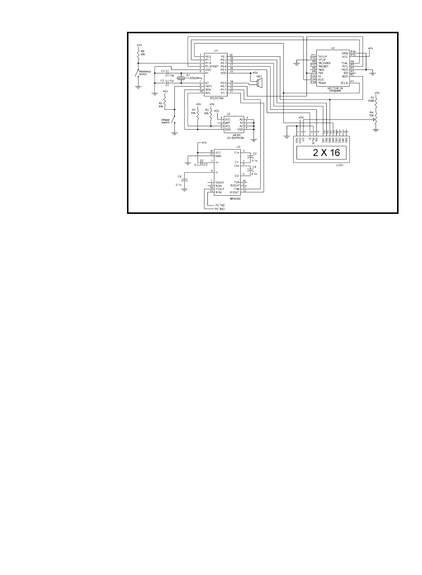
Figure 3 shows the necessary connec-
tions to the compass unit.
I added averaging to the compass
output to smooth the data. The logic
uses a simple running average of the
last four points read from the com-
pass. The difficulty was in processing
through the 0° to 360° transitions. An
average of two samples at 359° and
two at 0° lead you to believe the unit
was pointed south at 180°.
I chose the easy way out and set a
tolerance band at about the current
averaged value, 60°. If the average
value is 300° to 359°, all entries in the
table between 0° and 59° are convert-
ed to 360° to 419° prior to extracting a
new average. If the average value is
between 59° and 0°, all entries in the
table between 300° and 359° are con-
verted to –59° to –1°. This seems to
work, but the tolerance band needs to
be set based on how rapidly the com-
pass may be moved.
I use the LCD in 4-bit interface
mode with the read/write line tied
low to make it a write-only interface
from the processor. In this mode, the
processor needs to wait after every
operation to make sure the LCD is
ready for the next one. A timeout of 5
ms for position and clear commands
is used. A 160-µs delay occurs follow-
ing the output of the two nibbles that
make up the 8-bit data word. A pin is
dedicated to the enable line (E) and
the control/data (RS) line, although
the RS can be shared. Four lines from
the processor communicate the data
nibble.
The I
2
C memory uses a 16-bit
address with the upper three bits
being forced to 0 to limit addressing
to 8192 bytes. Communication to the
device begins by the processor arbi-
trating for the I
2
C bus; that’s always a
win for the 87LPC764 because no
other masters exist.
This arbitration process involves
the issuing of a Start command by the
processor. This is a unique configura-
tion of the clock and data lines where
the data line is driven low and the
clock line is left high. Without this
condition, nothing can begin. Now
you know why leaving the resistors
off these lines will kill everything.
The I
2
C memory chip slave address
(1010000xb) is then output. The 1010,
or “Ah”, portion of the address desig-
nates an EEPROM chip and the 000
portion is the address of this chip as
selected by address pins A0 through
A2. And last, the x is a 0 for a write
from the processor or 1 for a read to
the processor.
Additional EEPROM chips would
have different LSBs for an address.
Different I
2
C types of devices would
have a different MSB. It’s a pretty
smooth system.
The master device always drives
the clock line, in this case the ’764
processor. Either the master or slave
may drive the data line depending on
the direction of the data transfer. The
I
2
C memory device will pull the data
line low on the ninth pulse of the
clock line from the processor. This is
the gratifying response called
acknowledge. Lacking this one little
pulse can make life extremely diffi-
cult. If the address is incorrect for the
memory chip, it will not pull the line
low but will sit quietly expecting
some other device to handshake with
the processor.
After it acknowledges, the master
and slave are synchronized. This
acknowledge bit is used bidirectional-
ly. The receiver of the data will pulse
this bit to indicate a good transfer
(most of the time). If the receiver is
finished receiving data, it won’t pulse
this bit on the last byte transfer. This
is a signal that the transfer is com-
plete, and a stop condition should fol-
low. The stop condition is another
unique configuration of the data and
clock lines where data goes low to
high while the clock stays high. This
stop condition places the memory
chip in a low-power standby state.
Writing data to the EEPROM is
easy. The processor issues the chip
address (0A0h), two bytes of the mem-
Figure 3—
The Yard-Stick doesn’t
require many components.

22
Issue 130 May 2001
CIRCUIT CELLAR
®
www.circuitcellar.com
ory address, and then up to 32 bytes
of data. The EEPROM will normally
respond with acknowledges to these
bytes. The EEPROM won’t acknowl-
edge if the Write Protect pin is set, or
if the voltage is too low (3.6 V or less),
or if it’s busy with a previous write.
None of these conditions should
occur in the Yard-Stick, but to be safe,
the software will loop and retry any
operation lacking an acknowledge.
This is not a foolproof solution but
will salvage the cases in which the
processor tries to write to the memo-
ry too quickly.
Reading is more complex. To read
randomly, the processor needs to start
by telling the memory that it is writ-
ing. The processor issues all of the
addresses to set up the write and then
changes the sequence to issue a
repeated start with a read instead of a
write address. This repeated start is a
way of changing modes on the bus
without relinquishing it.
The first part of this sequence looks
like a write loaded into an internal
address register in the EEPROM and
the second part actually reads the
data. If the first part of this sequence
is not executed, then the word read
will be one up from the last word
written. Reads can continue until the
processor is satisfied, at which time it
will skip the last ACK and issue a
stop condition. Philips provides some
excellent software that performs all of
these tasks with a few lines of code.
I use software to debounce the
unit’s switch closures. Timer0 is set
up as an 8-ms interrupt timer. It
keeps a bunch of counters running to
time out messages
and time debounce
intervals. When a
wheel interrupt
occurs, the inter-
rupt processing rou-
tine immediately
halts further inter-
rupts. Next, it does
all of the updating
and memory storage
required, sets a flag
warning it needs to
be debounced, and
then exits.
The timer inter-
rupt looks at this flag and begins
interrogating the state of the switch.
It insists that the switch stays open
for x (currently 4) consecutive sam-
ples in this timer routine. (A sharp
reader will notice that the unit can’t
actually function at 34 mph with this
debouncing. Then again, I know of
few gardeners who can run 34 mph.) If
the timer notices that the switch is
closed, it will restart this open count-
er. When the open counter is satisfied,
the timer routine will clear any left-
over pending wheel interrupts and
then re-enable the wheel interrupt.
The process between the two con-
tinues this way while data recording
is active. Data recording is deactivat-
ed in the main loop by turning off the
wheel interrupt. Prior to turning it on
again, the timer clears any pending
interrupts from the wheel. The push-
button switch is processed similarly
except that closures are recognized by
polling in the main loop. As soon as a
closure is recognized, a debounce flag
is set and the timer routine clears it.
DEVELOPMENT PROCESS
I generally shy away from using
OTP units because most of mine
work improperly. I remember one
year when my Christmas tree was
decorated with expensive OTP units
(each one with a different but still
wrong program). Basically, I’m too
cheap to buy an emulator, so what
was the answer? The answer turned
out to be the old If statement.
I developed all of the software and
hardware except the I
2
C memory
using a pair of ancient ’51s in the
classic burn and crash mode running
on a prototype of the Yard-Stick
(see Photo 5).
I checked out the I
2
C interface
using an 87C752. The ’51 lacks the
I
2
C interface and the ’752 lacks the
internal memory needed. I put the
application code into the ’51 with a
macro for all accesses to memory.
When running in the ’51 environ-
ment, the macro uses the upper 128
bytes of its 256-byte memory to simu-
late the external memory. When run-
ning on an 87LPC764, the macro uses
calls to the I
2
C memory routines.
When it came time to burn the first
’764, I started sweating.
With the first one, there were two
problems that required some effort to
solve, but all in all it worked well.
The first problem was that the ’764
initializes onboard memory to FFs,
rather than 0s like the ’51. I had not
initialized a few counters, so some of
the messages had –1s in them.
I should have solved the second
problem earlier. The I
2
C routines use
more stack space than I anticipated
and I had squeezed the stack between
R7 and RAM address 20h (where the
flags were). When the I
2
C routines
were called when the stack was deep,
the stack would write over a few
words of the flags. The only symptom
was a few LCD flashes, processing
continued normally most of the time.
The program restarted unexpectedly a
few times. I finally thought to exam-
ine the stack space with the examine
command, and lo and behold, the zero
word I had hoped to find in cell 1Fh
was gone. I moved the stack out of its
position and expanded it, and the
problems disappeared. I have only two
ornaments for next year’s tree.
MECHANICS
I wanted a small, lightweight device
for the Yard-Stick. The LCD deter-
mined case size. It has to be readable
at a far distance, which means large
characters and a large display for just
2 lines × 16 characters. The case and
wheel assembly, made from 0.5
″
PVC
pipe and plastic, are mounted on a
shaft. I wanted a wheel closure every
6
″
, so I used a wheel with 12
″
circum-
ference (3.819
″
diameter).
Figure 4—
The plot of the flower bed came out well with only a bit of editing
required to close the curve. I suspect that a gimbaled compass would remove
the errors preventing a perfect plot.
– 25
– 20
– 15
– 10
– 5
5
– 30
– 40
– 50
– 20
– 10
10
10
0
0
– 30
F
eet
Feet
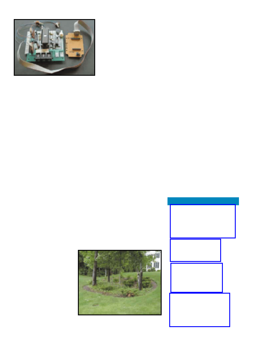
24
Issue 130 May 2001
CIRCUIT CELLAR
®
www.circuitcellar.com
I put two small magnets in the hub
of the wheel and put the reed relay in
the PVC pipe that served as the axle.
A bicycle handle grip made a nice
addition, and a coat of red paint hid
the PVC pipe. The wires for the
switch run through the pipe and exit
to plug into the back of the case. The
assembly is glued together except for
a few critical joints that are made
with screws. The screws allow the
unit to be disassembled and stored in
a small space. Two of the mounting
joints are unglued, allowing you to
adjust the case to make sure the com-
pass runs level to the ground.
USING THE UNIT
Using the Yard-Stick is easy and
fun. I recommend calibrating every
time the unit is turned on. Press the
switch for 2 s, then turn around keep-
ing the unit level, and end up facing
180° from where you started. Press
the switch again and the unit will dis-
play the waiting message and a sec-
tion summary message.
Now, position the unit to the start-
ing point in the first section to be
recorded and press the button.
Walk the outline of the area
keeping the unit level, and press
the button again when you come
back to the starting point.
Repeat this process for all areas
you wish to measure.
Then, turn off the power and
connect the unit to your PC.
Select the Hyperterminal soft-
ware and configure for a VT100
terminal with added line feeds.
Select 9600 bps, 8 bits, no parity,
and 1 stop bit. Turn on the unit
and you should see an “S-” dis-
played. Select “Capture to Text
File” in HyperTerminal and then
type “X”. The unit will transfer
the data. If you are an Excel per-
son, you can write a program to
convert and plot the data. If you
are a graphics person, then you
can convert the data to import to
your program.
If I can stop exploring all of
the ’764’s neat features, I may
complete this part of the project
and provide some software. But
that’s another challenge and
probably not as much fun.
RESULTS
I first tried mapping the driveway. I
ran the device around it a couple of
times and the readings were repeat-
able to 1
′
in the 500
′
circumference.
Plotting it proved a surprise. Every-
thing looks good including the sharp
little hook down by the street and the
square area in the back for the snow-
plow. When I got to the garage doors,
everything went haywire.
The plot indicated the driveway
should be heading into my neighbor’s
yard. This puzzled me until I realized
that there were three cars parked
about 1 to 2
′
behind those doors.
That’s a lot of metal to toss a com-
pass. Someday I’ll move all of the cars
and try it again.
Looking for an area free of large
metal masses, I tried a flower bed
next. I used the Yard-Stick to map
this bed, read the data into an Excel
spreadsheet, and then plotted it again
(see Figure 4). Photo 6 shows the
flower bed for comparison to the plot.
The beginning and ending points were
David Penrose is a management and
engineering consultant in Bedford,
New Hampshire. He has an M.S. in
Computer Science and holds an Extra
Class Amateur radio license
(AA5QL). His experience includes
more than 30 years with a major
aerospace corporation and more
recently as vice president of systems
and technology for a high-tech, start-
up company. You may reach him at
penrose@mediaone.net.
SOURCES
MAX202
Maxim Integrated Products, Inc.
(408) 737-7600
(800) 998-8800
Fax: (408) 737-7194
www.maxim-ic.com
HyperTerminal software
Hilgraeve Inc.
(734) 243-0576
www.hilgraeve.com
87LPC764 microprocessor
Philips Semiconductor
(212) 536-0500
Fax: (212) 536-0559
www.philips.com
off, but not by much. Most of that can
be chalked up to not keeping the unit
level on the slope around the bed.
NEXT
You can probably replace the Vector
2X compass with some of the newer
semiconductors that provide the same
functionality. I’m not sure if the oth-
ers have the same resolution or accu-
racy, but I’ll take a look at them. The
ultimate device probably would be a
combination of this unit and a GPS
system to get absolute as well as rela-
tive location. I have a couple of GPS
units with serial output ports. I guess
with the few words of program space I
have leftover in the 87LPC764, I can
squeeze in a bit more functionality.
But that’s next year’s contest.
I
Photo 6—
I started plotting the flower bed from the closest point
shown in this photograph.
Photo 5—
The prototyping breadboard with the ’87C51 checks
out the software and hardware. The ribbon cable connects a
mounting board for the compass module.
26
Issue 130 May 2001
CIRCUIT CELLAR
®
www.circuitcellar.com
ou are all famil-
iar with the simple
BFO (beat frequency
oscillator) metal detector
(see Figure 1). The operation of such a
detector is based on the comparison of
the frequencies of a reference oscilla-
tor and another oscillator that incor-
porates an inductive sensor in its
tuned circuit. The comparison is usu-
ally done by mixing together the two
oscillators. Ferrous or nonferrous
metal brought near the sensor
changes its inductance, which in turn
changes the frequency of the search
oscillator, and the difference in the
frequency appears at the output of the
mixer. The result can be heard in
headphones or displayed visually,
depending on the construction.
We found that the BFO metal detec-
tor requires objects to be three to four
times closer than other techniques.
One problem is the spurious mutual
synchronization of the two oscilla-
tors, which makes it impossible to get
a small frequency difference.
We decided to create a device that
has the same simplicity of construc-
tion as the BFO detector, but without
its main faults of low sensitivity and
inability to distinguish between fer-
rous and nonferrous targets. The heart
of the idea is to measure the search
oscillator’s frequency directly with a
frequency meter and process the
results with optimal digital filtering.
THEORETICAL
CONSIDERATIONS
The frequency meter approach is
shown in Figure 2. Let’s discuss the
operating sequence. First, the frequen-
cy meter measures the search oscilla-
tor frequency while the sensor is far
from any target, and this value is
placed in memory. Then, the frequen-
cy meter measures the search oscilla-
tor in real time. The previously stored
master frequency is subtracted from
each reading and the result is
processed for the readout.
Any spurious mutual synchroniza-
tion of the two oscillators will be less
likely, because now the search oscilla-
tor’s frequency (tens of kilohertz) is
three orders of magnitude less than
the frequency meter’s time base fre-
quency (tens of megahertz).
It is now possible to measure the
magnitude of the frequency difference
and its sign, which gives the detector
the ability to distinguish between fer-
rous and nonferrous metals. When the
target is primarily ferrous, it increases
the sensor inductance, causing the
search oscillator frequency to
decrease. The conductivity of nonfer-
rous targets causes the sensor induc-
tance to drop, causing the search
oscillator frequency to increase.
The uncertainty in the frequency
measurement arises primarily from
two sources, the short-term stability
of the time base and the quantization
error of the measurement itself.
Quartz oscillators have good short-
term stability, so they can be ignored.
FEATURE
ARTICLE
Finding hidden treas-
ure might not be what
Andrei and Yuri had in
mind for this metal
detector project, but
whether you’re look-
ing for the hardware
to start a salvage
company or just look-
ing for an interesting
project to build, this
design is worth more
than its weight in gold.
Andrei Chtchedrine &
Yuri Kolokolov
Frequency Meter
Metal Detector
y
Photo 1—
The complete metal detector (except for
power supply and sense coil) fits comfortably on a 45
× 72 mm circuit board.
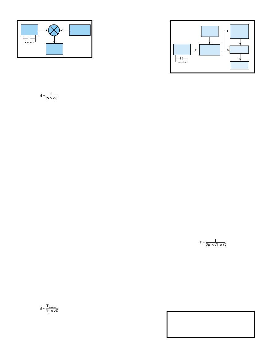
www.circuitcellar.com
CIRCUIT CELLAR
®
Issue 130 May 2001
27
The quantization error is given by:
[1]
where N = T
0
× F
x
, the number of
counts given by an input frequency
(F
x
) over a measuring interval (T
0
).
Equation 1 shows that there are two
ways to reduce the quantization error:
increase the search oscillator frequen-
cy or increase the measurement inter-
val. One reason not to increase the
former is that the frequency is chosen
to maximize the response from desir-
able targets and minimize the
response from the ground and envi-
ronment. Most metal detectors use 5-
to 70-kHz frequencies.
The measuring interval should be
chosen so that the measurements
seem instantaneous, so that you get a
real-time response as you sweep the
sensor. The measurement interval
should not exceed 40 ms. [1]
For a search frequency of 10 kHz
and a measurement interval of 40 ms,
Equation 1 gives a quantization error
value of about 0.001. This means that
you can distinguish frequency
changes of only about 10 Hz, which
isn’t much better than the sensitivity
of the BFO technique.
However, there is another approach
to measure the period of the search
oscillator instead of its frequency. To
get even better accuracy, you can
measure several periods. Now the
quantization error is given by:
[2]
where T
1
= M × T
x
(M periods of the
input period T
x
) and T
master
is the peri-
od of the master clock being used to
measure the period.
If T
1
is 30 ms (300 periods of a
10-kHz signal) and T
0
is 0.1 µs, the
uncertainty is just 1.36 × 10
–6
,
which is significantly better than
the BFO approach.
This means you need to change
the algorithm shown in Figure 2;
the box marked “Frequency meas-
urement” needs to become a peri-
od meter that measures the search
oscillator’s average period instead
of its frequency.
PRACTICALITIES
Obviously, if such a device were to
be realized with small- or medium-
scale integrated circuits, it would be
complex and cumbersome, thus
impractical for mobile operation.
However, this is an excellent applica-
tion for a microcontroller, which can
take on the task of measuring the
period and all of the functions relating
to processing the results (calculating
the period differences and providing
audible and visible indications).
We selected a microcontroller based
on the following criteria, in decreas-
ing order of importance: high clock
frequency; available 16-bit timer with
Capture mode; cost; power consump-
tion; hardware and software develop-
ment tools; and miscellaneous (pack-
aging, temperature range, etc.).
After evaluating a number of possi-
bilities using these criteria, we select-
ed Atmel’s AT90S2313-10PI. This 8-
bit RISC microcontroller is economi-
cal to operate. It provides 10 MIPS of
performance at an operating frequen-
cy of 10 MHz. It contains 2 KB of in-
system programmable flash memory,
128 bytes of EEPROM, 15 I/O lines,
and 32 working registers. Two
timers/counters, a watchdog timer,
analog comparator, and universal seri-
al port are available, too.
We managed to completely imple-
ment our design in this microcon-
troller with a small amount of exter-
nal hardware. The results are shown
in Photo 1. The circuit board is
only 45 × 72 mm. In spite of its
size, the device has excellent per-
formance (see Table 1).
Figure 3 shows screen dumps
from a digital oscilloscope that
demonstrate sensitivity and
selectivity. For these trials, the device
was connected to a computer via a
serial interface. A search coil consist-
ing of 100 turns of 0.47-mm wire
(approximately AWG 24-ed), 190 mm
in diameter was connected to the
metal detector. The displayed value is
the relative change in the period of
the search oscillator. The sample fre-
quency is about 36 Hz. Two different
targets were tested, a 25-mm diameter
copper coin and a 100-g iron object.
The sensor was moved over the target
three times in each trial.
CIRCUIT DETAILS
Now, it’s time to describe how the
various sections operate. Figure 4
shows the detector. The search oscil-
lator is based on D1, an NE555 timer
chip. This device works perfectly at a
supply voltage of 4 V or greater. The
resonant circuit consists of capacitors
C1 and C2 along with the sensing
coil. The resonant frequency is deter-
mined by the formula:
[3]
where C is the serial combination of
C1 and C2.
It isn’t necessary to calibrate the
oscillator frequency, because the
microcontroller firmware adapts to it
automatically. The frequency will be
about 25 kHz with the standard 100-
turn, 190-mm sensing coil and C1 =
0.047 µF and C2 = 0.01 µF. If neces-
Search
Oscillator
Reference
oscillator
Frequency
measurement
Master
measurement
memory
Subtract
Indication
Figure 2—
A metal detector based on an electronic frequency
meter avoids some of the problems of the BFO design.
Search
oscillator
Indication
Reference
oscillator
F1
F2
F1 – F2
Figure 1—
A BFO metal detector directly measures the
difference in frequency between two oscillators, one of
which incorporates the sensor coil.
Supply voltage
4.5 to 6 V
Current consumption 15 mA
Output indication
Eight LEDs and audio
Seek modes
Static and Dynamic
Discrimination
Ferromagnetic and non-ferromagnetic
Table 1—
Here are key specifications of the metal detector.
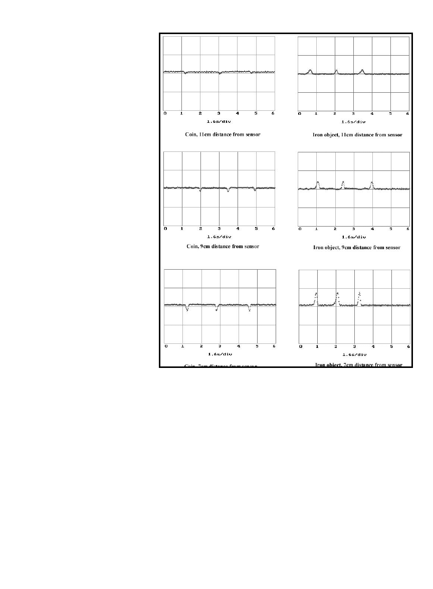
28
Issue 130 May 2001
CIRCUIT CELLAR
®
www.circuitcellar.com
sary, the frequency can be adjusted by
replacing C1 and C2, but try to keep
the ratio of their values in the range
of 4:1 to 6:1.
The AT90S2313 at D2 carries out
all of the remaining functions of pro-
cessing the search oscillator signal,
including the output indicators. The
industrial version, with a temperature
range of –40°C to 85°C, allows opera-
tion in the field environment even
when the temperature is low.
The control switches and audible
and visible indicators are connected
directly to microcontroller pins.
Switches S1 through S5 set the oper-
ating mode. LEDs VD1 through VD3
show the drop in search oscillator fre-
quency when a ferrous object is
detected. For other conductive
objects, LEDs VD5 through VD7 show
the increase in frequency. LED VD4
indicates a zero frequency shift.
LED VD8 lights if the device finds a
target while in Dynamic mode. This
mode takes some time between find-
ing a target and recognizing its type.
This indication tells you to fix the
position of the target more precisely.
Piezoelectric buzzer Y provides an
audible indication of changes in the
search oscillator period. The circuit
consists of few components, and there
are no special requirements for any of
them. The microcontroller D2 should
be socketed. You can change the
AT90S2313-10PI to AT90S2313-10PC,
but then operation below 0°C would
not be guaranteed, and such cold tem-
peratures are possible in the field. The
resistors are not critical, and can be
0.125- or 0.25-W units.
Capacitors C1 and C2 should have a
low temperature coefficient, especial-
ly C2. There are no special require-
ments for the remaining capacitors,
and any package can be used.
You should perform the six steps
for checking out the assembled device
in the correct order. First, examine
the circuit carefully for assembly
errors. Second, take the microcon-
troller out of its socket and apply
power to the circuit observing polari-
ty. Third, verify that there is oscilla-
tion at pin 3 of D1 at the expected fre-
quency (about 25 kHz for the given
component values).
Fourth, switch off the supply and
put the microcontroller into its sock-
et. Switch on the supply again and
measure the current consumption. It
should be no more than 15 mA at 5 V.
Fifth, place the sensor as far as possi-
ble from metal objects and push the
Reset button S0. Sixth, verify the
indications as various objects are
brought near the sensor.
MICROCONTROLLER
OPERATION
Because most of the device’s func-
tions are based on software, the
design effort focused on the firmware.
Figure 5 shows the main tasks the
microcontroller implements.
One special feature of the algorithm
is that the program adjusts itself to
the actual operating frequency of the
search oscillator. The theoretical lim-
its that the firmware can accommo-
date run from 153 Hz to 588 kHz.
Immediately after starting, the micro-
controller measures how many signal
periods occur in 6553.6 µs. Then, this
value is multiplied by 4 or 17,
depending on the mode of operation.
This gives the number of periods (M)
to measure during actual operation.
Later, periods of the search oscillator
signal will be measured with 0.1-µs
resolution. For any starting frequency,
this interval will be close to 26 ms (or
111 ms).
Figure 3—
These oscillograms demonstrate the sensitivity and selectivity of the detector. The vertical scale corre-
sponds to the full internal dynamic range.
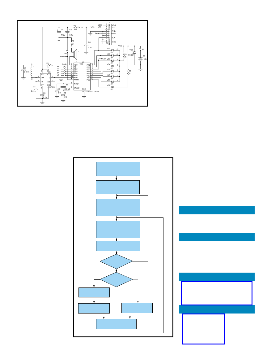
www.circuitcellar.com
CIRCUIT CELLAR
®
Issue 130 May 2001
29
Andrei Chtchedrine lives in Moscow,
Russia. He earned a degree in
automation and electronics from
Moscow Engineering Physics
Institute. Currently, he heads the
automation division of Inpred Co.
You may reach him at aish@aha.ru.
Yuri Kolokolov lives in Donetsk,
Ukraine. He has 14 years of experi-
ence in circuit design and embedded
controllers. Currently, he is a senior
manager at Comis Ltd. His technical
interests include nonstandard elec-
tronics projects. You may reach him
at yukol@bigfoot.com.
The first measurement of the signal
is remembered as the master value.
This value is subtracted from subse-
quent measurements, giving a result
that indicates how much the search
oscillator period has changed from its
starting value. This is a form of A/D
conversion. The result is called the
digital input signal.
In Static mode, the loga-
rithm of the digital input
signal is taken and used to
drive the indicators. Each
level of LED illumination
is accompanied by a corre-
sponding tone.
As stated before, the
self-calibration is accom-
plished immediately after
the microcontroller starts.
However, the search oscil-
lator frequency may drift
under the influence of
such destabilizing factors
as temperature or soil con-
ditions. If the mean of the
last 16 measurements
exceeds the threshold, self-
calibration can be restarted
automatically if this mode
is switched on.
The Dynamic mode is
designed for searching for
targets when there is inter-
ference from the ground,
minerals, and so on. In this
mode, the digital input sig-
nal is filtered to produce a
user-friendlier signal. Our
device uses a technique
called optimum matched
filtering. Briefly, the main
idea is this: There is an optimum fil-
ter for any signal, and this filter pro-
vides its maximum output when this
signal is present. In the metal detec-
tor, the signal for all actual targets
has approximately the same shape
(see Figure 3) and differs only in sign
and amplitude. The same filter can be
used for all targets. Our software uses
a non-recursive, matched, optimum,
ninth-order filter. After filtering, the
signal is sent to the indicators as
described for Static mode.
When assembled, the source code
occupies 418 words of program mem-
ory, which is less than half of the
available capacity. This level of effi-
ciency for such a complex algorithm
illustrates the effective instruction set
and easy-to-use peripherals of the
AVR microcontrollers that allowed us
to accomplish some of the tasks in
hardware. Also, this leaves room for
additional improvements and features
in the firmware.
I
Rough frequency measurement,
using 65536-ms interval.
Result is M
Determine measurement interval
T= M/N, where N = 4 or 17
(about 26 or 111 ms)
Measure time required for
T periods of input signal,
in units of 0.1 µ us.
Result is a 24-bit quantity T et
Calculate difference
T work = T work – T et
Self-calibrating?
Self-calibrating?
Mode?
Ninth– degree optimum
matched filter
Threshold
comparison
Threshold
comparison
Generated audible and visible
indications
Static
Dynamic
No
Yes
Measure time required for
T periods of input signal,
in units of 0.1 µ us.
Result is a 24-bit quantity T work
Figure 5—
Most of the detector functions happen in the firmware.
REFERENCE
[1] A. Chtchedrine, I. Osipov, Metal
Detectors for Hunting Buried
Treasures and Relics, Radio and
Communication, Hot Line
Telecom, Moscow, 1999.
SOFTWARE
The source code is available on the
Circuit Cellar
web site. Visit home.
skif.net/~ykol for future upgrades.
Figure 4—
The
diagram of
metal detector
shows the sim-
plicity of the
hardware.
RESOURCE
B. Dvoriashin, L. Kuznetcov,
“Radio Technical Measurements,”
Soviet Radio
SOURCE
AT90S2313
Atmel Corp.
(408) 436-4270
Fax: (408) 436-4314
www.atmel.com

30
Issue 130 May 2001
CIRCUIT CELLAR
®
www.circuitcellar.com
hen I built my
weather station,
which I described in
“A Low-Cost Weather
Station” ( Circuit Cellar 122), I always
intended to experiment with other
kinds of anemometers. There was
space on the top of my weather sta-
tion pole, spare wires in the ground,
and room on the LCD. I was search-
ing the Internet for information about
other types of anemometry when I
came across some descriptive ads for
ultrasonic anemometers. That was it,
I was hooked. I had to build one.
ORIGINAL PLAN
Soon after deciding to embark on
this project, I found some reference
articles that discussed a theory [1] and
a complete project.[2] For background
information, read the “Underlying
Theory” sidebar.
For a nanosecond, I considered
duplicating a project that Neil Dvorak
created years ago. [2] Then, my ego
got in the way and a new design was
conceived. Don’t we all get an attack
of the “I can do it better” syndrome
from time to time? Neil Dvorak’s
project influenced my design, but
there are also many differences
between the two projects.
I decided this project should make
use of the HC11’s built-in timer sys-
tem, a feature which was lacking in
the vintage Z80 used by Dvorak. [2]
The transmitter (Tx) and receiver (Rx)
circuitry would use an HC11 operat-
ing in Single Chip mode and reside on
top of my weather station pole in an
appropriate enclosure. Power would
be supplied from the existing weather
station power supply. Transit time
data would be sent via the SPI serial
system to the HC11 in the house for
subsequent processing and display.
This seemed like a workable design.
At this point, the only question was,
would line drivers and receivers be
required on the SPI serial link?
With this plan in mind, I began
building the circuitry that would
form the heart of the new anemome-
ter. Because this project would even-
tually use the HC11 in Single Chip
mode, I included a header so that all
development could be done with the
HC11 development system running in
Expanded mode. After the code was
finalized, the HC11 would be pro-
grammed and installed.
Work proceeded as per this plan for
some time. I built the Tx/Rx system
first, leaving space in case additional
circuitry is needed in the future. I had
to wait to work on data transmission
until there was actual data to send.
Initial testing of the Tx/Rx circuit
was done with some low-cost Murata
transducers. Although Murata’s trans-
ducers aren’t weatherproof, I assumed
I could either weatherproof these or
use them in a way that protects them
from the weather. I also considered
using them without modification, and
simply replacing them when they
failed. However, after many napkin
designs, I concluded that off-the-shelf
weatherproof transducers made the
most sense. But….
REALITY CHECK
Because I started my project think-
ing that I would solve the weather-
proof problem later, the Tx/Rx circuit
was already in revision number two
before I decided to use off-the-shelf
weatherproof transducers. Prices for
weatherproof transducers vary consid-
erably ($50 at the low end). I needed
FEATURE
ARTICLE
When Gordon leaves
extra space in a
design for “future
improvements” you’d
better believe that
additional features are
on the way, it’s only a
matter of time. All it
took was the mention
of ultrasonic anemom-
etry and he was ready
to update his weather
station project.
Gordon Dick
Ultrasonic Anemometry
Anyone?
w
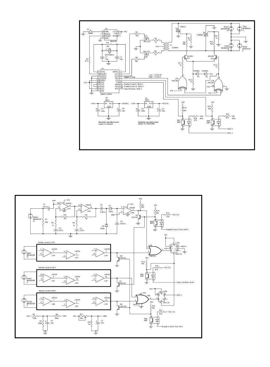
www.circuitcellar.com
CIRCUIT CELLAR
®
Issue 130 May 2001
31
eight, so that’s about $400.
Spending that kind of money
on a woodworking tool, rifle
scope, or dog is OK, but not
on a weather station!
So, do I quit? Just forget all
of the effort expended so far?
I considered quitting, but
decided to complete it with-
out making it weatherproof.
Sadly, this project will not
grace the top of my weather
station pole.
TRANSMITTER TROUBLE
Much of the paper design
worked fine without revision.
Some parts didn’t though,
which was no surprise. First,
producing a clean tone burst
for the transmitter required
more attention. Initially it
was a gated oscillator; the
oscillator was a common
gate-based circuit with a 40-kHz crys-
tal and the gating was done using an
I/O pin from the HC11. Because the
40-kHz oscillator wasn’t synchronized
with the HC11, the tone burst usually
contained a truncated cycle at the
start and end. Even though it’s proba-
bly of no consequence, there must be
a better way.
Let the HC11 produce the tone
burst! And, the circuit gets simpler
when the gate-based oscillator is
removed. That’s excellent. I tried a
software loop first. Generating the
tone burst has to happen before any-
thing else happens. While that’s going
on, the HC11 has nothing else to do,
so generating the burst this way made
a lot of sense.
Although a tone
burst can be produced
this way, what’s needed
is a pair of burst signals
that are perfectly com-
plementary, because
the burst signals will
drive a pair of FET
switches in an inverter
circuit. Although
approximately comple-
mentary burst signals
can be produced this
way, there is too much
overlap at the edges,
which will cause both
inverter FETs to be on
at the same time. This
won’t work.
My next attempt pro-
duces good comple-
mentary burst signals.
The HC11 still pro-
duces the signals, but
it’s done using the
internal timing system.
The HC11 can produce
Figure 1—
Optical isolation and separate power sup-
plies help keep the T
x
circuit noise from finding its
way into the R
x
circuit.
Figure 2—
Four separate amplifier channels alternate to produce pairs of transit time signals.
Photo 1—
The pipe support-
ing the transducers is
mounted to the base so that
it can be rotated for align-
ment. The legs holding the
conduit are attached to the
base via screws in slots to
permit adjusting the separa-
tion of the transducers.
32
Issue 130 May 2001
CIRCUIT CELLAR
®
www.circuitcellar.com
a 40-kHz signal, but that’s near the
upper end of what’s possible using a
4.9152-MHz crystal.
In order for an ultrasonic transducer
to produce a chirp that will travel a
significant distance, it has to be driv-
en at a high voltage level. It’s not
uncommon for this drive voltage to be
300 V or more. Both [2] and [3] used
an audio transformer backwards in an
inverter circuit to produce the drive
signals. I sorted through several audio
transformers before finding one that
still had a useable signal at 40 kHz.
And, it worked adequately driving one
transducer. However, two parallel
transducers need to be driven. This
audio transformer had such high out-
put impedance that the drive voltage
was too low when two transducers
were connected.
So, it looks unavoidable, an invert-
er transformer has to be wound.
Fortunately, some ferrite cores and a
selection of enameled wire were avail-
able, so I designed and wound a trans-
former. My recollection now is that
the secondary was wound more than
once before the secondary voltage was
adequate. But it’s an excellent trans-
ducer drive transformer, easily pro-
ducing 100 V with no loading when a
second transducer is added.
The circuitry to switch between
pairs of transducers worked immedi-
ately. My design is similar to
Dvorak’s plan. [2] The final version of
the Tx circuit is shown in Figure 1.
(The optoisolators were added later.)
Now that a chirp can be produced,
testing can begin on the Rx circuit.
RECEIVER REVISIONS
Some serious gain has to be applied
to get a useable signal from a trans-
ducer receiving a chirp. I used a gain
of 1156 (34 × 34 = 1156) and that
seemed to be adequate. It’s tempting
to simply set up a single op-amp. [3]
But, using LM324, a single stage set
up for that much gain doesn’t have
enough bandwidth to handle 40-kHz
signals, so two stages were required.
A Schmidt trigger is usually used
with the Rx circuit to produce the
pulse that signals a chirp has arrived.
But, I left out the trigger, thinking
that the HC11 would ignore any chat-
ter and capture on the first transition.
However, my assumption was only
half-correct (more about this later).
When the Rx circuit was tested, I
observed significant noise. The noise
was present even with zero input to
the Rx amps, indicating that the noise
was likely being radiated directly into
the Rx circuit. Noise finding its way
in via the power supply was unlikely
because they were separate.
At this point, I wished I had used
co-ax for the Tx lines, also. Changing
this wire for a shielded twisted pair
made a dramatic improvement. While
I was dealing with the noise problem,
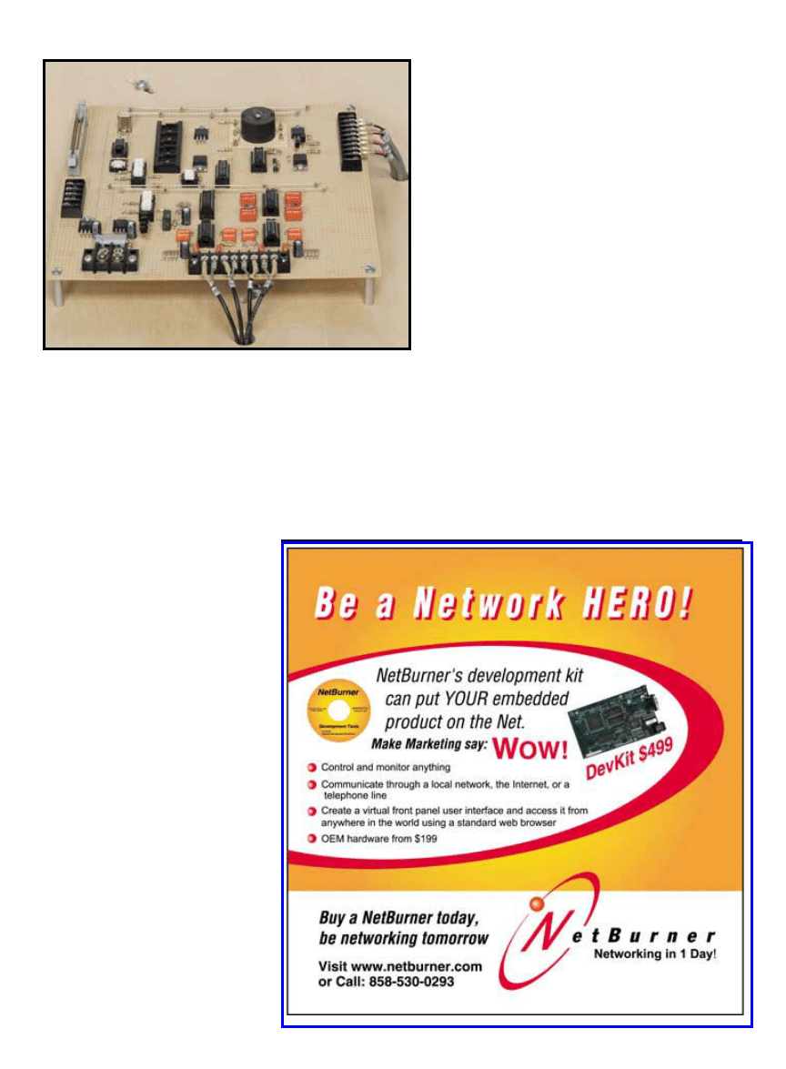
www.circuitcellar.com
CIRCUIT CELLAR
®
Issue 130 May 2001
33
Photo 2—
The Tx
circuitry occupies
the upper half and
the Rx circuitry
occupies the lower
half of the board.
The Tx transducer
connections are at
the top right and the
Rx transducer con-
nections are at the
bottom right.
Connection to the
development board
is via the header at
the top left. The con-
nections for the SPI
link are under this.
Power for the board
enters through the
bottom left section.
I decided to incorporate opto-couplers
to more completely separate the Tx
and Rx circuits. This eliminated a par-
ticularly troublesome burst of noise.
In my paper design, initially a ’157
multiplexed the pairs of pulses to the
HC11 input captures. But, I couldn’t
get it to work properly. Testing it in
isolation indicated it worked as adver-
tised, but it behaved strangely in the
Rx circuit.
So, I changed the multiplexing
scheme to what you see in Figure 2,
which is more complicated. The FF
(U10) was added last. Prior to that,
the measured delay times fluctuated
too much.
Eventually, I realized that the com-
parator (U3) outputs were chattering
and the HC11 was capturing more
than the first transition (remember
that earlier assumption?). The chatter
could be observed, but only if I was
looking for it! Now it appears I could
have avoided a lot of circuit modes
and troubleshooting if I had included
a Schmidt Trigger in the beginning.
Because the envelope detector cir-
cuit and comparator were intricately
combined, I didn’t make these com-
parators Schmidt triggers. That’s why
U10 was added; it sets on the first
edge from U4 and stays set until it’s
reset in preparation for the next burst.
INTEGRATED SYSTEM
Although I haven’t talked about
code much yet, you understand that
there needs to be many pieces of test
code created in a project like this. I
don’t have space to discuss each
piece. Mainly, I want to stress the
importance of proceeding systemati-
cally and in small steps. Many times
it was useful to revert to an earlier
version of code that worked in order
to properly assess the problem with
the newest version that didn’t work.
For some time, it was difficult get-
ting the whole system working. My
initial intent with this article was to
convey specifics about the coding
mistakes I made. However, I don’t feel
as forthcoming now. So, let me sim-
ply say that I can still make mistakes
that are too serious for someone who
isn’t an amateur. My current excuse
is that I’ve been away from the HC11
for some time learning about PIC
micros, so I’m a bit rusty. That’s my
story and I’m stickin’ to it.
Eventually, the whole system
worked. Photo 1 shows the system
with the transducers mounted to
arms and the Tx/Rx board in position,
and Photo 2 displays a close-up view
of the Tx/Rx board. There are now
four transit time measurements that
are correct on the LCD. They are still
in hex, but the measurements are
happening and the fluctuation in tran-
sit time is only three or four counts
with no averaging. And, when I sup-
ply wind using my shop vac, the tran-
sit times change as expected. You
gotta love it!

Two runners-up will receive a Handspring Visor
Two runners-up will receive a Handspring Visor
Two runners-up will receive a Handspring Visor
Pick a category and
submit your project by
w w w. c i rc u i t c e l l a r. c o m / D L 2 0 0 1
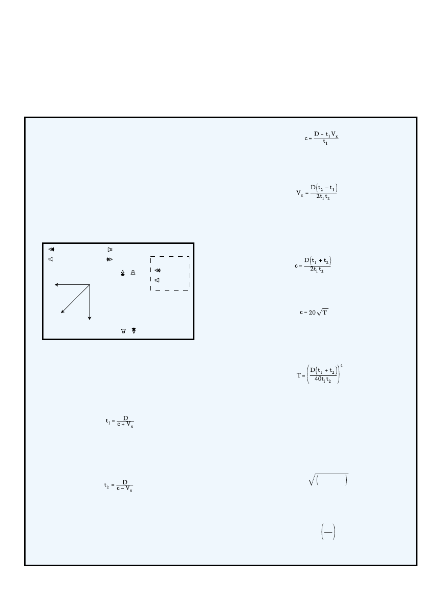
www.circuitcellar.com
CIRCUIT CELLAR
®
Issue 130 May 2001
35
There’s more number crunching to
do before wind speed and direction
can be displayed. But before that,
because the system finally works and
no more modifications are required,
it’s time to take a walk through the
Tx and Rx circuits.
Tx CIRCUIT OPERATION
The HC11 is shown on the Tx
schematic, (see in Figure 1), simply
because there was enough room there.
The HC11 is involved in both the Tx
circuitry and Rx circuitry operation.
The real-time interrupt (RTI) of the
HC11 controls the initiation of a tone
burst, which happens here at a 37.5-
Hz rate. A tone burst consists of 10
cycles of a 40-kHz square wave. A
complementary pair of burst signals
drives the gates of Q1/Q2 and the pri-
mary of T1.
Tone burst amplitude becomes
about 200 V peak-to-peak across the
[s3]
Substituting this value into Equation s2:
[s4]
At this point, you have the x component of the
wind. If you keep going and substitute the expression
for V
x
back into Equation s2, the following results:
[s5]
The speed of sound in air is related to temperature:
[s6]
where T is measured in kelvin. [4] If this value for c is
substituted in Equation s5, you get:
[s7]
This is an interesting result! It says that you can
measure the air temperature using the same transit
time data that will be used to measure wind speed.
After you obtain V
x
, you can see that V
y
will be
solved similarly using transit time measurements
from the NS pair of transducers. And the magnitude
of the wind vector is:
[s8]
And, the angle of the wind vector is:
[s9]
θ
= tan
– 1
V
y
V
x
V =
V
x
2
+ V
y
2
UNDERLYING THEORY
Suppose that a pair of transducers is oriented in the
east to west direction (along the x axis) and another
pair is oriented in the north to south direction (along
the y axis). Also suppose that the wind is blowing and
is resolved into an x component (V
x
) and y component
(V
y
), as shown in Figure s1.
Initially consider only the EW pairs of transducers
and the V
x
component of the wind. D is the transducer
separation, c is the speed of sound in air, t
1
is the transit
time for a chirp in the east to west direction, and t
2
is
the
transit time for a chirp in the west to east direction.
Sound traveling east to west is aided by the V
x
com-
ponent of the wind, and takes t
1
seconds to travel the
distance (D):
[s1]
Sound traveling west to east is retarded by the V
x
component of the wind, and takes t
2
seconds to travel
the distance:
[s2]
Now you have two equations with two unknowns.
The unknowns can be solved simultaneously for V
x
and c because t
1
and t
2
are known (transit times meas-
ured by the micro). Solving Equation s1 for c, you get
Legend
Transmitter
Receiver
Wind
V
x
V
y
NS Pairs
EW Pairs
θ
Figure s1—
The x component of the wind is measured by the EW
transducer pairs and the y component is measured by the NS
transducer pairs.

36
Issue 130 May 2001
CIRCUIT CELLAR
®
www.circuitcellar.com
Rx amplifiers use op-amps designed to
operate without a negative supply.
Although the LM324 is intended for
single-supply operation, it still
requires biasing. That’s the purpose of
the V
AA
supply in Figure 2. The pairs
of amplifiers (e.g., U1C/U1D) all have
a 2.5-V DC input that the received
chirp signal gets superimposed on.
Because the DC gain for each
amplifier is unity, the DC bias at the
input is not amplified at the output.
And you are able to let the DC output
of one become the input bias for the
next. As I said earlier, the AC gain for
the pairs is high.
FINAL CALCULATIONS
I didn’t create code for this last
phase. The desire to continue spend-
ing time and effort on a project that
would only exist as an article was fad-
ing. However, I’ll take you as far as I
went with it.
From the underlying theory [1], the
expression for V
x
expressed in meters
per second is:
secondary of T1. Q3 and Q4 and their
associated gate circuitry provide a
clever way to apply the burst to one
or the other pair of transducers via a
single control line from the HC11. [2]
For example, the W and S may chirp
first, and then on the next RTI, the N
and E chirp.
After a chirp is produced, the HC11
waits for interrupts. When the Rx gets
a pair of received chirps, a pair of ris-
ing-edge pulses gets applied to the
input capture system via IC1/IC2
through optoisolators ISO1 and ISO2.
The time between sending and receiv-
ing the chirp is measured to obtain a
pair of transit times. On the next RTI,
a different pair of transducers will
produce chirps and a different pair of
transit times will be measured, and so
operation of the Tx circuit continues.
Rx CIRCUIT OPERATION
Some circuits in the Rx circuit are
replicated four times. You can see this
clearly in Figure 2. This means there
are lots of components to wire and a
busy schematic. However, operation
of the Rx circuit is straightforward. If
the W and S transducers have chirped,
then the E and N Rx amplifiers
should be active and the W and S
amplifiers should be disabled.
Amplifiers are disabled via Q5 to Q8,
which also operate in pairs. This
scheme works because the LM339 is
an open-collector device.
This disabling is necessary because
receiver transducers adjacent to a
transmitting transducer produce a
large signal coincident with the chirp,
which is not the signal of interest.
Received signals are amplified by two
stages of gain followed by an envelope
detector and comparator.
A comparator output going high is
passed via an OR gate to a D-type FF,
which sits on the first edge and
ignores any subsequent noise edges.
During every RTI, the D FFs are
cleared and the pair of active ampli-
fiers is switched. Optoisolators are
again used to keep the Tx and Rx cir-
cuits separate.
Because this project was to be pow-
ered by an existing 14-V supply, the
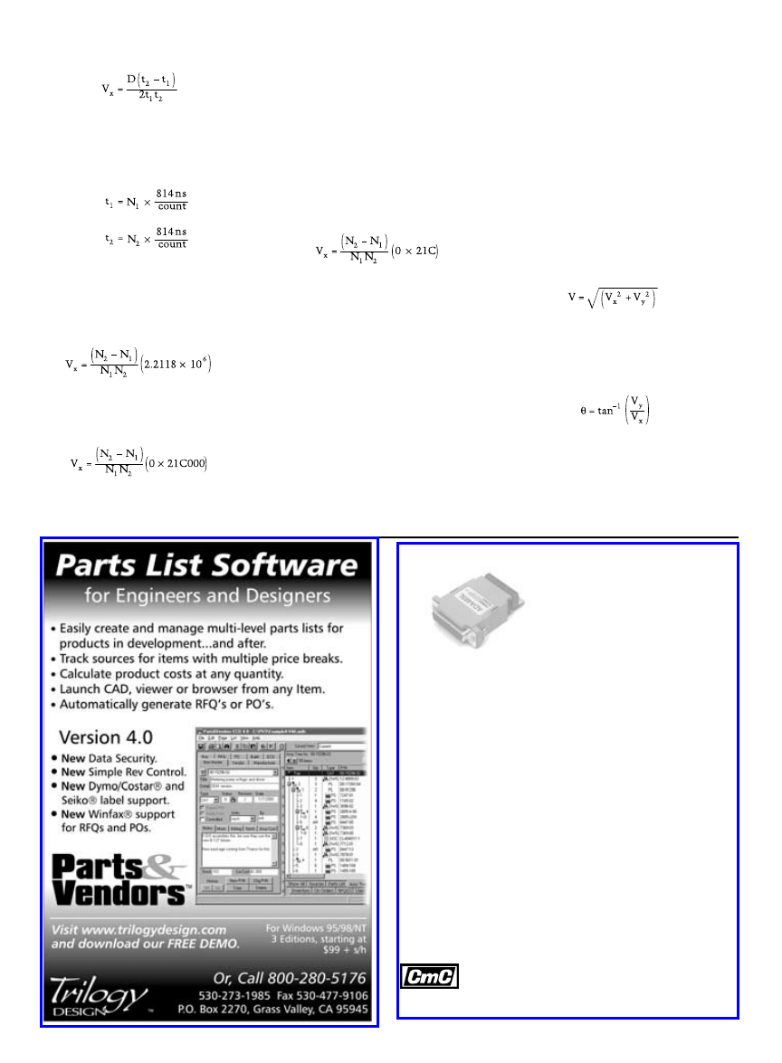
www.circuitcellar.com
CIRCUIT CELLAR
®
Issue 130 May 2001
37
[1]
Transit times t
1
and t
2
will be meas-
ured as count values using the inter-
nal timing system:
[2]
Substituting these for V
x
using D = 1
m and converting to kilometers per
hour gives:
[3]
And, when the conversion factor is
converted to hex:
[4]
You can see that the numbers are
going to be awkward. The denomina-
tor requires a 16 × 16 bit multiplica-
tion, which isn’t available as an HC11
instruction. Also, the conversion fac-
tor is larger than 16 bits and it needs
to be multiplied by a 16-bit quantity.
However, if the numerator and
denominator are divided by 16
3
, V
x
becomes:
[5]
where the hexadecimal point in the
32-bit denominator is moved three
places to the left by a combination of
truncating and rounding after the
multiplication. This leaves both a
denominator and numerator that each
easily fit into 16 bits (check some typ-
ical numbers).
So, the only troublesome aspect is
the 16 × 16 bit multiplication.
Because I had created a routine to do
this, I thought it would be easy.
Testing this approach with some typi-
cal numbers indicated that the error
from truncating and rounding would
be insignificant. However, this
approach will work only up to about
20 kph before the numerator gets larg-
er than 16 bits and the division won’t
work anymore.
This is when I stopped. It appears I
need a division routine that handles a
numerator larger than 16 bits.
As soon as you obtain the compo-
nents V
x
and V
y
, you want to calcu-
late the magnitude using Equation s8
(for the overall wind speed):
[6]
and find the angle using Equation s9
(for the wind direction):
[7]
A look-up table may be the best
approach for the inverse tangent func-
tion. Anyone have a square root rou-
tine for the magnitude? Another pos-
AD422 (Requires 9VDC) $79.00
AD422-1 for 110VAC
ADA485 (requires 9VDC) $79.00
ADA485-1 for 110VAC
CMC’s low cost converters adapt any
use with RS422 or RS485
devices
• Adds multidrop capability to
ADA425 (requires 9VDC) $89.00
ADA425-1 for 110VAC 99.00
Mention this ad when you order and deduct 5%
Use Visa, Mastercard or company purchase order
WWW.2CMC.COM Fax:(203)775-4595
PO BOX 186, Brookfield,CT 06804
Connecticut microComputer, Inc.
38
Issue 130 May 2001
CIRCUIT CELLAR
®
www.circuitcellar.com
sibility is to express the magnitude in
terms of sine or cosine and then use a
series expansion for the trigonometry
function. Either way it’s a fair amount
of work. As I said, this is when I
stopped, but if any of you build this,
I’d love to hear about how you dealt
with these last steps.
ROOM FOR IMPROVEMENT
Usually, after a circuit works, you
can find many areas for improvement,
and this project is no different. If you
decide to tackle an ultrasonic
anemometer of your own, consider
some suggestions.
A PIC-type micro can measure the
transit time because there isn’t a lot
of I/O. Therefore, the micro would
occupy less board space and U5
wouldn’t be required. If the calcula-
tions for magnitude and direction are
done using a different micro, then you
don’t have to code a 16-bit multiply
in the PIC-type micro.
Also, the circuit used to switch
between transducer pairs can be sim-
plified by eliminating Q5/Q6 and U7.
Let the micro control the triac gates
directly using two I/O lines.
A double-sided PCB with a good
ground plane should help eliminate
some of the noise present on the wire-
wrapped version. You may be able to
remove all of the optoisolators.
A single wide-BW op-amp can
replace the pair of oldies that I used.
That eliminates quite a few passive
components, as well.
In addition, it’s a good idea to
switch U3 to a newer comparator (not
open collector) and make it a Schmidt
trigger. With the addition of a
Schmidt trigger, I’m certain a ’157-
style multiplexer would work proper-
ly to multiplex between receiver
pairs. Thus, you could replace U4,
U10, and Q5 through Q8 with a single
multiplexer chip.
There may be additional improve-
ments you can implement. Have fun
finding them!
I
REFERENCES
[1] J. H. Robertson and D. I. Katz,
“ Climatronics’ Novel Sonic
Anemometer,” Ninth Joint
Conference on the Applications
of Air Pollution Meteorology
with Air and Waste Management
Association, Atlanta, GA, 1996,
American Meteorological
Society, Boston, MA.
[2] N. Dvorak, “ Sonic Anemometry
for the Hobbyist,” Byte
Magazine
, July 1979.
[3] D. R. Herrington, “ Ultrasonic
Range Finder Uses Few
Components,” EDN, June 24,
1999.
[4] W.J. Humphreys, “ Physics of the
Air,” McGraw-Hill, New York,
NY, 1926.
SOURCES
Murata Electronics
(770) 436-1300
Fax: (770) 436-3030
www.murata.com
68HC11
Motorola, Inc.
(847) 576-5000
Fax: (847) 576-5372
www.motorola.com
Z80
Zilog, Inc.
(408) 558-8500
Fax: (408) 558-8300
www.zilog.com
Gordon Dick is a physical engineer
and is an instructor of computer engi-
neering technology at Northern
Alberta Institute of Technology,
Canada. Occasionally, he consults in
the area of intelligent motion control
and is usually working on an elec-
tronics project. You may reach him at
gordond@nait.ab.ca.
www.saelig.com • saelig@aol.com
see what’s new at www.saelig.com!
CAN Boards for almost any form factor: PCI, ISA, PCMCI,
/PC104, VME, compact PCI format, etc. Drivers for WIn95
WIn98, WinNT Win2K ,VxWorks, pSOS, Lynx, Linux, OLE,
FT8U232AM serial <> USB FT8U245AM 8bit <> USB
This PC runs under almost any OS:

Atmel's programmable FPSLIC SOC technology
speeds time-to-market while lowering risk
for a true out-of-body experience.
Set yourself free on your next design
project. Let Atmel's FPSLIC devices
give you inner peace with FPGA,
bytes of SRAM on a single chip.
Need to get to market fast? No problem.
System Designer™, our co-verification
based design tool, will take months off your
development schedule. And with stand-by current
under 100 µA, you won’t need divine intervention
to meet the power goals of your portable products.
market. For more information and to order your
starter kit, go to www.atmel.com/ad/fpslic02.html.
Fax-On-Demand:
(800) 292-8635 (North America)
(408) 441-0732 (International)
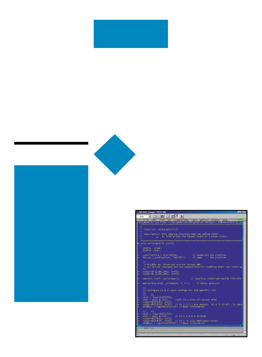
40
Issue 130 May 2001
CIRCUIT CELLAR
®
www.circuitcellar.com
Photo 1—
Although this is
putting the cart before the
horse in a sense, it’s still a
good depiction of what the
Paradigm Debugger win-
dow looks like and what
strings you can pull with it.
he Arcom SBC-
386EX-S is at home
on an industrial RS-
485 network. Arcom has
gone to great lengths to make the
embedded developer’s SBC-386EX-S
experience a good one. All of the dirty
work of installing and configuring the
three core software packages is done
up front. In SDK
form, Arcom’s
SBC-386EX-S is
ready to roll rightly
out of the box.
Last month, I
examined the hard-
ware features of
the SBC-386EX-S
and loaded the soft-
ware suite onto a
desktop PC in the
Florida room. This
time, I’ll put all of
the embedded
hardware and soft-
ware to work on
the Florida-room intranet. Get ready
to meet the performers in this three-
part play with a surprise ending.
ACT I: SUPERTASK!
SuperTask! is code that is combined
with the original developer’s source to
form a multitasking application. That
means SuperTask! is not an applica-
tion. Instead, it is an embedded-ori-
ented set of computing tools designed
to ultimately reside on a platform like
the SBC-386EX-S and exist inside the
embedded ROM or flash memory.
Embedded developers can concentrate
on writing the specific device-level
code needed for their applications.
SuperTask! controls how the user-
written routines are scheduled and
run in an application’s big picture.
Multitasking implies the execution
of many computational jobs, or tasks,
handled concurrently by a single
CPU. You already know that a CPU
can only perform one task at a time,
so multitasking is really the division
of work, usually based on time,
between many tasks under the con-
trol of one CPU. There are several
pages dedicated to the construction of
viable multitasking systems. Such
devotion to one subject indicates that
writing multitasking applications is
not a trivial task.
Once again Fred is
digging into an SBC
offering from Arcom
and once again he
shows us that embed-
ded doesn’t have to
be difficult. This per-
formance has a cast
that includes Borland
C++, SuperTask!,
Treck TCP/IP, and
Paradigm’s Remote
Debugger.
Fred Eady
Return of the SBC
Multitasking Applications with
SBC-386EX-S
t
APPLIED
PCs
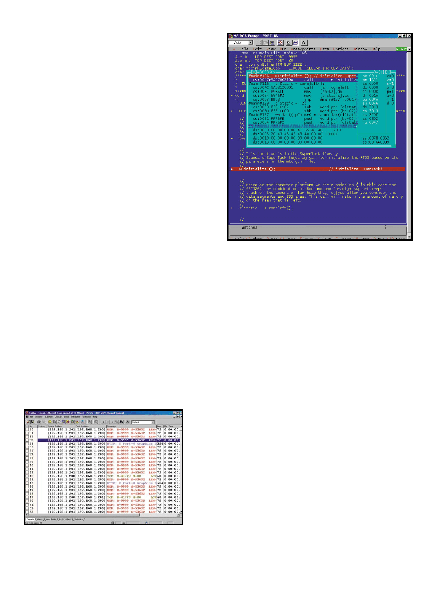
www.circuitcellar.com
CIRCUIT CELLAR
®
Issue 130 May 2001
41
SuperTask! contains a multitasking
executive called MultiTask!, which
assists in the design of complex mul-
titasking applications by allowing you
to break down the application into
smaller, simpler tasks. MultiTask!
also allocates various CPU and mem-
ory resources, which allow the appli-
cation to manage events that the
application is monitoring or control-
ling. The allocation process is not
automated by MultiTask!, it is con-
trolled by the developer. The applica-
tion developer controls memory dis-
tribution and time slicing. MultiTask!
simply applies these rules to form a
functional real-time multitasking
application. MultiTask! supports both
preemptive priority-based task sched-
uling and round-robin time-slicing.
Each task is treated as one thread, and
multiple threads can execute in the
multitasking process concurrently.
MultiTask! is shipped with a source
and make file, which allows you to
fashion it yourself. In the SBC-386EX-
S SDK, this is already done, and
MultiTask! is optimized for the SBC-
386EX-S platform. But, the embedded
developer has programmatic control
over how the MultiTask! executive
operates within an application. A set
of ANSI C system functions allows
you to control such parameters as the
amount of execution time a thread is
allowed to have and the amount of
memory it can consume.
To incorporate the SuperTask! and
MultiTask! executives into an appli-
cation, you must initialize MultiTask!
in the
main() func-
tion and pass con-
trol to it. Any C
function in the
application can be
treated as an inde-
pendent task. To
illustrate the
process of incorpo-
rating SuperTask!
and MultiTask!, I’ll
show you a series
of code snippets
that will ultimately
be assembled in a
working multitask-
ing application
under the supervi-
sion of MultiTask!
routines.
Good programs are written top-
down, so I’ll start at the top beginning
with the includes. Earlier I stated that
Arcom did all of the up-front work.
This is evident in the
include file area
of Listing 1. Basically, the Arcom
includes are reflections of the Arcom
port. For instance, in the
ArSockets
include file, the standard sockaddr_in
socket structure is defined as ar_sock-
addr_in. Also, many of the standard
calls in the SuperTask! and Treck
TCP/IP modules are cross-referenced
to standard or Borland conventions.
Speaking of Borland, the SBC-386EX-S
SKD uses the Borland C++ 5.0 compo-
nents for the compilation
and linking tasks.
Taking another look at
the Arcom include area,
you can get a feel for what
hardware features of the
SBC-386EX-S can be
exploited. Without going
into detail, the
ArUsxUtl.h
entry points to SuperTask!
Usx
refers to United States
Software, the makers of
SuperTask! Between the
Ins8250.h and ARCOMm.h
files, all of the serial I/O
functionality on the SBC-
386EX-S can be included in
your application. Because
this is a multitasking real-time hard-
ware and software set, the
ArRtc.h
and
ArTmr.h files in conjunction with
the
ArSystem.h and ArMemory.h defini-
tions provide the necessary precision
timing and memory management data
structures and routines MultiTask!
needs. If required by your application,
the Flash File System is represented
by the
ArSff.h include file. The last
two include files,
ArTcpIp.h and
ArSocket.h, are obvious as to their
presence and importance if the SBC-
386EX-S is expected to ride the ’Net.
Just as Listing 1 gives away the
available SBC-386EX-S hardware func-
tionality, Listing 2 does a good job of
describing what the multitasking
environment will be juggling. Super-
Task! needs the external definitions
to allocate dynamic memory and
attach the SBC-386EX-S real-time
clock to the MultiTask! timing algo-
rithms. The five tasks that will be
running are outlined with some sup-
porting definitions for the two “talk-
er” tasks shown at the bottom of
Listing 2. The
_pColor pointers denote
dynamic and static memory when
memory management is handed off to
SuperTask! The colors are SuperTask!
terms, with color0 referencing static
memory and color1 representing
dynamic memory. Static memory is
Photo 2—
This shot gives
you a feel for the Paradigm
Debugger system details
window.
Photo 3—
Line 45 shows that 564 bytes of data were sent by tcptalker.
Checking the Sniffer stats, 510 out of 564 bytes were data. Between
lines 34 and 45, the udptalker sent nine datagrams each, with a data
payload of 30 for a total of 270 bytes of data.
42
Issue 130 May 2001
CIRCUIT CELLAR
®
www.circuitcellar.com
allocated and reserved and dynamic
memory is used and then dumped
back into the memory pool for reallo-
cation and subsequent reuse.
The TM that precedes some of the
defines is a holdover from the Treck
core definitions. The names don’t
need to be specific to Treck. Basically,
I’m defining the message size, desti-
nation IP address, destination ports
for both UDP and TCP communica-
tions, and the data that will be trans-
mitted to each port. 192.168.1.200 is
actually a Linux server running
Apache on a segment of the Florida-
room intranet.
Let’s talk more about the five tasks
that are predefined in Listing 2. A
task is actually a C function, but not
just any C function. A is task a C
function that is treated as a task by
invoking the function using the
MultiTask!
runtsk() function. Each
task is endowed with its own stack
space and CPU register set or context.
Tasks in this environment don’t rely
on other tasks and, thus, run inde-
pendently. If a task is inactive or
#include <ArExtern.h>
// Globals defined elsewhere
// Borland include files.
#include <stdio.h>
#include <dos.h>
#include <string.h>
#include <mem.h>
#include <stdlib.h>
#include <stdarg.h>
#include <math.h>
#include <alloc.h>
#include <conio.h>
// SuperTask! include files.
#include <ArRtos.h>
// Arcom include files.
#include <ArTypes.h>
#include <ArSystem.h>
#include <ArMemory.h>
#include <ArUsxUtl.h>
#include <ArComm.h>
#include <ArSff.h>
#include <ArRtc.h>
#include <ArTmr.h>
#include <Ins8250.h>
#include <ArTcpIp.h>
#include <ArSocket.h>
Listing 1—
The
ArRtos.h
includes embody all of the macro definitions that have to do with the
SuperTask! and MultiTask! executives.
success of embedded
designs—and configurability
is key to the right BIOS.
detailed information and a
free sample BIOS binary for
your standard
reference
design.
What do the leading silicon
vendors know about BIOS
© 2000 General Software, Inc. All rights reserved.
Full source code automatically
configured with over 400 para-
meters using BIOStart
Windows 95/98/CE/NT
Embedded, Linux, DOS, and all
x86-based operating systems
www.gensw.com •sales@gensw.com • 800-850-5755 • 425-454-5755
Call 530-297-6073 Fax 530-297-6074
Get connected at www.jkmicro.com
DOS & Web server pre-installed
Realtime multitasking available with eRTOS
In-Circuit-Programmable Xilinx CPLD
512K SRAM, 512K Flash standard

www.circuitcellar.com
CIRCUIT CELLAR
®
Issue 130 May 2001
43
waiting, it is not using CPU
resources. That’s a good thing. A good
thing that could turn out to be a bad
thing is that task has access to global
variables and can alter them in such a
manner as to upset a companion task
in the application. But, local variables
within the task and any function
called by it are considered private to
the task.
The task information is kept in a
task control block, or TCB. The TCB
contains information about the task’s
context, queue link, and state. An
array of TCBs is created when Super-
Task! is initialized. A nonexistent
TCB doesn’t have an associated task.
When
runtsk() in invoked against a
function, that function becomes a
task that is associated with a TCB in
the array. The task is then exposed to
the system.
killtsk() is run against
the task to return it to its basic func-
tion status and terminate it. The slain
task is then hidden from the system
and the TCB it occupied is released.
When a task is introduced to the
system via the
runtsk() function, it is
put into a running or ready state. The
highest priority task in this state is
the only task running. Tasks can be
suspended using the
suspend() func-
tion. Using
suspend() temporarily
blocks the task from running with no
detriment to other tasks.
Tasks also can be classified as wait-
ing. In the waiting state, like the sus-
pend state, the task doesn’t use any
CPU resources. A waiting task can be
in any queue except the Run queue.
The Time Delay queue is where the
task waits for a time period to elapse.
Each item a task can wait on has an
additional Wait queue, and this is
what makes the Limbo queue unique.
Tasks in the Time Delay and Limbo
queues can be set to both wait and
suspend at the same time. There are a
number of other queues and a matrix
of states that go along with them. The
subject of tasks, states, and queues is
covered in the SuperTask! manual for
those of you who will employ the
SBC-386EX-S, or are simply curious.
ACT II: THE APPLICATION CODE
This portion of your multitasking
application is hosted by Borland C++
5.0 and underwritten by Datalight.
You already know the Borland com-
piler. And, Datalight is a deity when
it comes to embedded tools and oper-
ating systems. If Datalight is new to
you, browse through some of my past
articles in Circuit Cellar.
I’ll focus on the content that the
Borland C++ code is compiling and
linking. The SuperTask! installation
instructions ask that the developer
run some basic tests using canned
SuperTask! routines to make sure that
the hardware platform is acclimated
to the SuperTask! and MultiTask!
executives. Again, Arcom has already
taken care of this. And, the Arcom
SDK installation process has placed
everything in the right place so that
the major application packages,
Borland C++, SuperTask!, Treck
TCP/IP, and Paradigm Remote
Debugger, all cooperate towards the
common goal of creating a multitask-
ing embedded application.
Arcom’s pre-integration and porting
puts you close to starting SuperTask!
and firing up your application. The
first order of business is to prepare the
SBC-386EX-S hardware platform. This
vArSemaInit ();
// Arcom Semaphore Processing
//
// Initialize the onboard serial communications ports.
//
wArInitCpuComs();
// Initialize CPU board serial coms
//
// This initializes the Arcom Flash File System. The routines
are based on the calling conventions that Borland/Microsoft used
for their DOS based file I/O.
//
wArSffInit ( );
// Flash File System.
//
// Initialize the onboard Real Time Clock. Select US time format
//
vArRtcInit(1);
Listing 3—
Using the
vArSemaInit()
function, Arcom put one additional layer on the SuperTask! event
and resource facilities. Events and resources are allocated on a queue basis. This eliminates the need to
keep track of who had what and when as far as events and resources are concerned. A simple function,
evt = uArEvtNext ()
, will return the next available event from the RTOS.
extern ARRTC _ArRtc;
extern UINT32 _ulDynamic;
void far MainTask();
void far vHmi();
void far FileTest();
void udptalker();
void tcptalker();
SINT16 wTestDone;
UINT8 *_pColor0;
UINT8 *_pColor1;
//talker definitions
#define
TM_BUF_SIZE
30
#define
TM_DEST_ADDR
"192.168.1.200"
#define UDP_DEST_PORT
9999
#define
TCP_DEST_PORT 80
char commonBuffer[TM_BUF_SIZE];
char *ccink_data_udp = "CIRCUIT CELLAR INK UDP DATA";
char *ccink_data_tcp = "CIRCUIT CELLAR INK TCP DATA";
Listing 2—
The MainTask runs with all of the other tasks as subordinates. The vHmi task allows the SBC-
386EX-S to be accessed and manipulated via Telnet. The talker tasks are simply demonstrations of how
easy it is to implement multitasking network-oriented jobs.
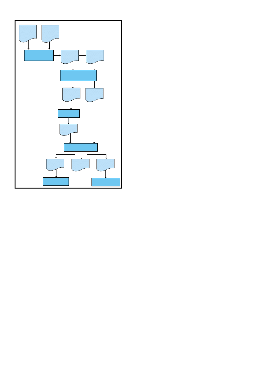
44
Issue 130 May 2001
CIRCUIT CELLAR
®
www.circuitcellar.com
is “automagically” done using
Arcom’s
vArTargetInit() function. It’s
backwards to show you the results of
a compile in a debug session before
actually talking about the compile
process, but hang in there with me on
this one.
Photo 1 is a shot of the
vArTargetInit() function as seen
through the view port of the Paradigm
Debugger. Various calls to ports and
SBC-386EX-S hardware features are
used to put the SBC-386EX-S into a
known state that is acceptable for
starting the MultiTask! executive.
The initialization of the hardware
sets the stage for the startup of the
SuperTask! RTOS. The next function
to be executed is the
Mtinitialize()
routine. As you can see in Photo 2, I’d
be here for a while giving you a byte-
by-byte account of the initialization
process. Because I don’t have the time
nor space for a reverse engineering of
the code, I’ll move on.
After MultiTask! is
initialized,
coreleft()
is run and the free
memory is given to
SuperTask! to man-
age.
vArTargetInit()
doesn’t bother to ini-
tialize any of the
SBC-386EX-S com-
munications ports,
real-time clock mod-
ule, or Flash File
System. So, these
subsystems must be
initialized by hand.
Fortunately, the
Arcom
Ar functions
that come with the
SBC-386EX-S SDK
take “by hand” out of
the equation and per-
form the initializa-
tion jobs using pre-
written functions spe-
cific to the SBC-
386EX-S (see
Listing 3). Referring
back to the descrip-
tion of the Arcom
includes, you can
relate the origin of
the following func-
tions:
• WArInitCpuComs—initializes the
SBC-386EX-S serial ports
• WArSffInit—sets up the Flash File
System
• VArRtcInit—initializes the real-
time clock
At this point, the SBC-386EX-S
hardware is conditioned for Super-
Task! and all of the peripherals are
ready for work. It’s time to put the
pedal to the metal. The MainTask is
kicked off, the context switching is
tied to the Timer0 ISR, and Multi-
Task! is officially started. The Timer0
ISR link to the context switcher is
performed by a function called
vArUsxClk(), which implicates the
SuperTask! hook with an Arcom twist
in the source code for the function.
The same can be said of
MTstart(),
except there is no Arcom intervention
involved and
MTstart() is a
MultiTask! native call. At least one
task must be placed in the Run queue
before calling
MTstart(). Upon being
invoked,
MTstart() will immediately
start execution of the highest priority
task, in this case, MainTask. The syn-
tax for
runtsk() is:
runtsk (uint priority, void (*tskp-
tr), uint stksze,….)
The actual code looks like this:
runtsk (110,(void(*)(void))
MainTask,1024);
Now, everything inside the of
MainTask will begin execution.
Before you take a look at what’s going
to happen there, I want to put the
horse back where it belongs, in front
of the cart.
Listing 4 is the
make file used to
assemble and link the final applica-
tion you’ve been examining with the
Paradigm Debugger. The
make file can
be broken down into smaller sections
for easier reading. And, for additional
ease, I added comments for each sec-
tion and Figure 1 should lend a clearer
picture. Note that in the APOBJS
area, the talker tasks are not listed,
this is because they are local func-
tions that are called and invoked
using
runtsk() dynamically.
So far, I installed the SBC-386EX-S
software development environment,
read several pages of SDK documenta-
tion, wrote source code and, in some
cases, ported using Borland C++ 5.0.
As well, the
make file was generated
and the application was compiled and
linked successfully using Borland C++
5.0. Before the application is down-
loaded to the SBC-386EX-S using the
Paradigm Debugger, at this point in
the game I’m ready to run the applica-
tion and show you the results.
ACT III: THE TRECK TCP/IP
STACK
Just like the Borland C++ compiler,
there’s not much to say about Treck’s
TCP/IP stack. Like the Borland C++
compiler, the Treck stack is a superb
product with good industry creden-
tials. If you really want to understand
the mechanisms behind sockets and
networking the Internet from a pro-
Source
codes .c and
.asm
Include
files
.h
Borland bcc.exe
Borland tasm.exe
Object file
.obj
Library file
.lib
Borland linker
tlink.exe
.map
.rom
Arcom locit
.pdr
Paradigm locate
.axe
.loc
.exe
Paradigm debugger
pdrt186.exe
Final application in
flash memory
Figure 1—
Use this chart along with the file in Listing 4 to have a better under-
standing of what the SDK components do.
www.circuitcellar.com
CIRCUIT CELLAR
®
Issue 130 May 2001
45
APPL = CCINK
!ifndef MODEL
# Not Command line specified ?
MODEL=l
# Set Default
!endif
!ifndef DEBUG
# Not Command line specified ?
DEBUG=2
# Set Default
!endif
RTOS
= 1
# RTOS required
FLOAT
= 0
# Floating Point Emulation
OPTIMIZE
= 0
# 0 - none
WARNINGS
= 1
# 1 - all
PLATFORM
= SBC386
# SBC386 Hardware Platform
CODESTRING
= 1
# Put string literals in code segment
# Include the SuperTask! and Treck include directories in the
search path
USRINC = $(ARC_EMB)\include;$(USXSRC);$(TRKSUPINC)
# These object files are necessary for the complete application
APOBJS = Globals.obj \
Main.obj
\
hmi.obj
\
# Create hardware specific information to include proper lib files
for linking
!include $(ARC_EMB)\util\devpath.mkf
!include $(ARC_EMB)\util\Arcom.mkf # Compiler/linker Arcom cus-
tomization options
# This area creates application output and runs locate
$(APPL).$(OUT): \
$(APPL).rom
locit2 $(APPL) 880
locate $(PFLAGS) $*
if exist $(APPL).exe del $(APPL).exe
ren $(APPL).bin $(APPL).exe > nul
if exist globals.obj del globals.obj
# This area checks for dependencies. If files are not found, they
may be created
$(APPL).rom:
\
$(STARTUP)
\
$(APOBJS)
\
$(8250)\8250$(RTOS)$(MODEL).$(LIB)
\
$(LIBS)
\
$(ISDS)\Isds$(RTOS)$(MODEL).$(LIB)
\
$(TRECK)\source\trksrc$(RTOS)$(MODEL).$(LIB)
\
$(TRECK)\supp\trksup$(RTOS)$(MODEL).$(LIB)
\
$(USXUTL)\mod$(RTOS)$(MODEL).$(LIB)
# This area runs Borland's linker tlink
tlink $(LFLAGS) @&&! +
$(STARTUP) +
$(APOBJS)
$*.rom
$*.map
$(8250)\8250$(RTOS)$(MODEL).$(LIB)
\
$(LIBS
\
$(ISDS)\Isds$(RTOS)$(MODEL).$(LIB)
\
$(TRECK)\source\trksrc$(RTOS)$(MODEL).$(LIB)
\
$(TRECK)\supp\trksup$(RTOS)$(MODEL).$(LIB)
\
$(USXUTL)\mod$(RTOS)$(MODEL).$(LIB)
!
Listing 4—
This whole mess is easier to read and understand if you substitute CCINK everywhere you see
APPL to quickly give you a list of files this process generates. Libraries are named ISDS, TRECK, and USX-
UTL.
CHARGE ORDERS to Visa, Mastercard,
. Shipping and handling for the
Limited. NO COD. Prices subject
5 mm diameter T 1 3/4 LED.
3000 MCD ultrabright.
Water-clear in off-state.
Operates at 20 mA.

46
Issue 130 May 2001
CIRCUIT CELLAR
®
www.circuitcellar.com
grammer’s point of view, take a look
at “Introduction to TCP/IP” and
“Introduction to BSD Sockets” in the
user’s manual. This documentation is
available on the web site.
The Treck TCP/IP stack is integrat-
ed into the SBC-386EX-S SDK and
provides all of the services you would
expect from a TCP/IP stack system.
Instead of rehashing TCP/IP and its
components, I’d like to use the net-
working code residing within the
MainTask as a working example.
Before I regressed to show you the
make file, your application was begin-
ning to execute code in the MainTask.
The first thing that’s done within the
MainTask is to start the Treck
TCP/IP stack.
wIpNetStart() is called
after entering the necessary IP
addresses. Authentication parameters
are set using edtp as the user name
and ccink as the password. Remember
these because you’ll need them later.
In addition to your talker tasks, the
SBC-386EX-S will run a Telnet and
FTP server concurrently. These
servers are part of the Treck package
and that’s why you don’t see a
runtsk() for them. However, there
are
runtsk() functions for each of the
talkers and another
runtsk() function
to start the Telnet and FTP interface
task, vHmi.
The talker tasks are similar. I have
one talker that sends UDP datagrams
as fast as it can, and another that does
the same with stream data via a
TCP/IP connection (see Listing 5).
Basically, two sockets are formed, one
for UDP and another for TCP. The
UDP port and IP destination address
are arbitrary because UDP doesn’t
need a connection to operate like TCP
does. So, you can send UDP packets
into the wind at will.
On the other side of the equation,
TCP needs to do some handshaking
before it can send data, and that
forces the port and destination
address to be real. This is pointed out
by the connect function call in the
tcptalker source that’s absent in the
udptalker code.
To accommodate this, I simply
aimed the TCP data at well-known
Port 80 on the Linux/Apache server
machine. The idea here is to show
void udptalker(void)
{
int udpSocket;
struct ar_sockaddr_in udpdestAddr;
strncpy(commonBuffer,ccink_data_udp,30);
udpdestAddr.sin_family=AF_INET;
udpdestAddr.sin_port=htons(UDP_DEST_PORT);
udpdestAddr.sin_addr.s_addr=inet_addr(TM_DEST_ADDR);
udpSocket=socket(AF_INET,SOCK_DGRAM,IPPROTO_UDP);
while(1)
{
sendto(udpSocket,commonBuffer,TM_BUF_SIZE,0,&udpdestAddr,sizeof(udp
destAddr));
}
}
void tcptalker(void)
{
int tcpSocket;
struct ar_sockaddr_in tcpdestAddr;
strncpy(commonBuffer,ccink_data_tcp,30);
tcpdestAddr.sin_family=AF_INET;
tcpdestAddr.sin_port=htons(TCP_DEST_PORT);
tcpdestAddr.sin_addr.s_addr=inet_addr(TM_DEST_ADDR);
tcpSocket=socket(AF_INET,SOCK_STREAM,IPPROTO_TCP);
connect(tcpSocket,&tcpdestAddr,sizeof(tcpdestAddr));
while(1)
{
send(tcpSocket,commonBuffer,TM_BUF_SIZE,0);
}
}
void far MainTask( void )
{
//
// Startup the Treck TCP/IP stack with the given parameters.
//
vArSetEtherIP(192,168,1,201);
// Set my IP address
vArSetEtherSubnet(255,255,255,0);
// Set my Subnet mask
vArSetEtherGateway(192,168,1,1);
// Set my default gateway
wIpNetStart();
//
// Set Server processes authentications.
//
vArSetLogin("edtp");
// Set Login: string
vArSetPassword("ccink");
// Set Password: strin
//
// Start Server's
//
wArStartTelnet();
// Start Telnet server
wArStartFTP();
// Start FTP server
runtsk ( 100,
(void(*)(void))vHmi,
1024 );
runtsk ( 101,
(void(*)(void))udptalker,
1024 );
runtsk ( 101,
(void(*)(void))tcptalker,
1024 );
Listing 5—
I gave both talkers the same priority to illustrate how SuperTask! handles that situation.
www.circuitcellar.com
CIRCUIT CELLAR
®
Issue 130 May 2001
47
you the data via a Sniffer screenshot.
The payload is a string message that
is loaded into a common buffer area.
CURTAINS
In Photo 3, the http lines of the
data capture are actually the TCP
content. The Sniffer is configured to
view Port 80 data as http data. The
TCP lines you see are the true TCP/IP
acknowledgement sequences that
must take place in the TCP/IP con-
nection. If it looks like UDP talker is
really pounding TCP talker, you’re
being deceived. Each UDP line you
see on the capture list sends only a
single buffer of 30 bytes. Each http, or
TCP, line sends as many 30-byte
buffers as it can in its time slice.
That’s really not the point here, but I
wanted to show you how easy it is to
write multitasking applications with
the SBC-386EX-S using the pre-ported
software suite you get with the SDK.
Point your Telnet or FTP client
towards 216.53.172.209 to try out the
Arcom SBC-386EX-S. Use the user
name and password I told you to
remember earlier. Commit the IP
address to memory also, that’s where
you can go to test-drive the embedded
goodies from this series. When you
transfer that file or set the RTC from
your Telnet console, keep in mind
that it doesn’t have to be complicated
to be embedded.
I
TCP/IP stack
Treck, Inc.
(513) 688-0553
(800) 340-6648
Fax: (513) 688-0993
www.treck.com
RESOURCE
Paradigm C++ Debugger Interface
Paradigm Systems
www.devtools.com/pcpp/debug-
ger.htm.
Fred Eady has more than 20 years of
experience as a systems engineer. He
has worked with computers and com-
munication systems large and small,
simple and complex. His forte is
embedded-systems design and com-
munications. Fred may be reached at
fred@edtp.com.
SOURCES

Then choose from over 100 Hands-On
Computer Labs where you can work with
the hardware and software tools for specif-
ic applications, like this Lab on testing and
installing a Phytec netCON board in an
Embedded Internet Lab (right) or working
with compilers in a USB Lab (below)
A Division of ConVergence Promotions
Mission College, Santa Clara, California

For More Information and Registration
Don’t Miss this Great Learning Experience!
Get the inside information and hands-on training on topics like:
Special sessions for managers by MicroDesign Resources and
Introductory classes like: “Embedded for Dummies”
embedded and communications applica
50
Issue 130 May 2001
CIRCUIT CELLAR
®
www.circuitcellar.com
Figure 1—
At each clock
pulse, a fixed value (55° in this
example) is added to a phase
accumulation register. The
resulting phase is then con-
verted to amplitude with a
sinus look-up table and ADC.
he night I sat
down to write was
supposed to be one of
the best nights of the
year to see hundreds of meteors in the
sky. I checked the date in my diary
months ago, but the sky here in
France stayed unfortunately cloudy.
The good news is that it was a mar-
velous opportunity to spend the
evening on my PC writing the second
part of my DDS-GEN article!
Last month I explained the DDS-
GEN project—a high-
performance, 0 to
120-MHz generator
that uses direct digi-
tal synthesis technol-
ogy. We studied the
user interface subsys-
tem of this project,
the I
2
C-MMI, and
now are ready to dig
into the DDS genera-
tor itself.
DIRECT DIGITAL SYNTHESIS?
First I’ll define the DDS principles.
A DDS generator is a purely digital
circuit that can reproduce any period-
ic waveform at virtually any frequen-
cy, depending on the main clock fre-
quency and harmonic content of the
waveform. As shown in Figure 1, the
DDS generator is simple.
At each clock tick, a fixed amount
is added to a phase accumulator regis-
ter, modulo 360°. The resulting phase
is used as an index for a look-up table
that gives the signal amplitude for
each phase value. Then, the ampli-
tude is converted to an analog value
by an A/D converter and low-pass fil-
tered to exclude any harmonic above
the Nyquist limit. When used to gen-
erate a sinus signal, a DDS generator
with N-bits long phase registers can
generate any frequency from:
to
with a resolution of
where F
clock
is the frequency of the
main clock.
With DDS technology, because
everything is digital, it’s easy to
implement complex modulation
schemes as frequency shift keying or
phase shift keying. For the former,
FEATURE
ARTICLE
Lucky for us it was a
cloudy night in France
when Robert was
scheduled to write the
second part of the
article on his DDS-
GEN project! Don’t
miss out as he covers
everything from hard-
ware selection to soft-
ware design to proto-
type contruction this
month.
DDS-GEN
Part 2: The Generator
t
Phase
increment
register
+
Phase
accumulator
Sinus
look-up
table
DAC
Phase increment register :
Time
Phase
Sinus
0
1
2
3
4
5
6
7
8
9
10
11
12
13
14
15
16
17
0
55
110
165
220
275
330
385
440
495
550
605
660
715
770
825
880
935
0.000
0.462
0.819
0.991
0.940
0.676
0.259
– 0.216
– 0.643
– 0.924
– 0.996
– 0.843
– 0.500
– 0.044
– 0.423
0.793
0.985
0.954
55
1.500
1.000
0.500
– 0.500
– 1.000
– 1.500
0.000
1
3
5
7
15
17
9
11
13
Clock
Robert Lacoste
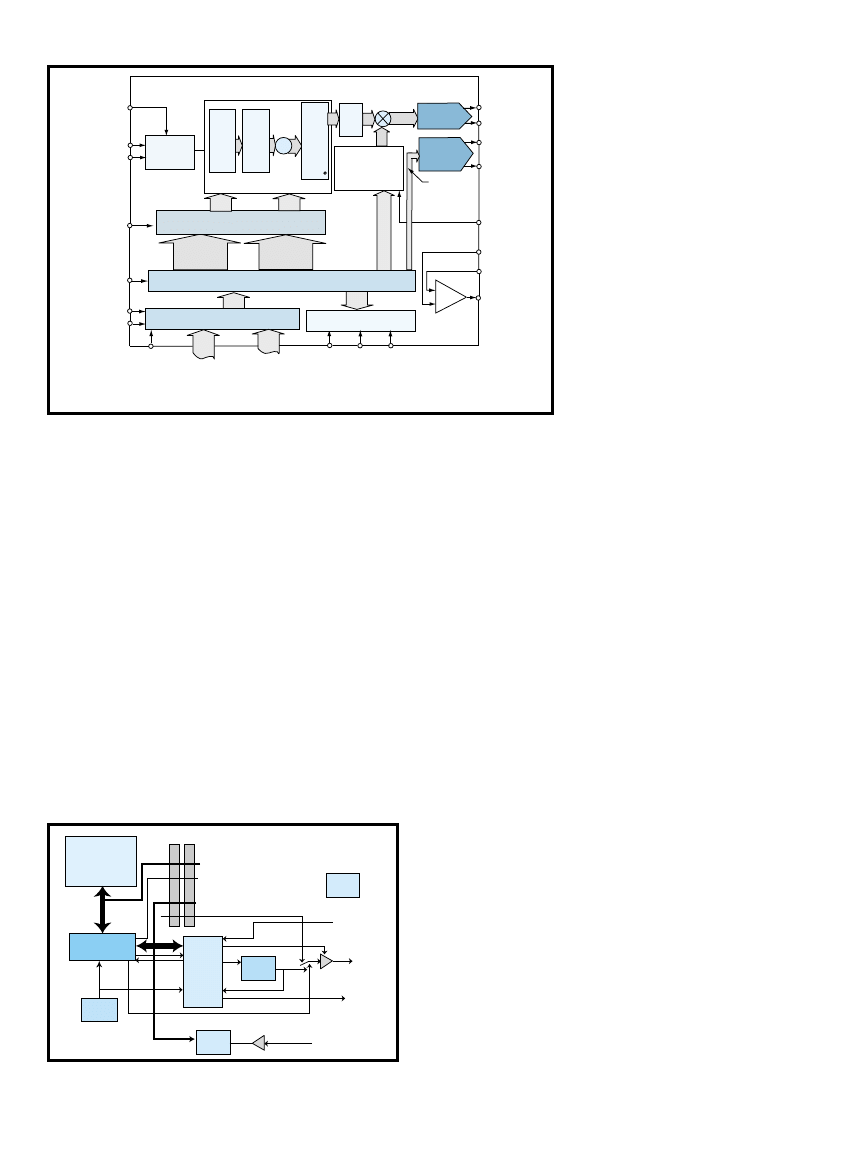
www.circuitcellar.com
CIRCUIT CELLAR
®
Issue 130 May 2001
51
swap between two phase increment
values, and for the latter, just add a
fixed value to the phase. The difficul-
ties start when you need a high main
clock frequency.
THE AD9852 MONSTER CHIP
It’s possible to design a DDS genera-
tor with discrete components or an
FPGA, or even with a full-software
implementation on a microcontroller
for low-speed applications. However,
some manufacturers have pretty
impressive dedicated DDS chips.
I chose the AD9852 for this project
(see Figure 2). [1] This 80-pin LQFP
chip integrates anything needed to
build a high-performance, DDS-based
sinus generator. And, the AD9852 can
be driven by a high-speed parallel bus
or SPI-compatible serial port.
Need speed? The AD9852ASQ has a
300-MHz maximum clock frequency
that can be internally generated
thanks to an on-chip clock multiplier.
The output frequency is limited only
by Nyquist (150 MHz) and the slope
of the external low-pass filter. A
lower grade version, the AD9852AST,
is limited to a reasonable 200 MHz.
The phase registers are 48-bits long,
giving a microhertz resolution for sig-
nals up to the maximum frequency.
This chip also integrates a pair of 12-
bit DACs (one is genera-purpose) as
well as a high-speed comparator to
generate low-jitter
square signals.
Around the DDS
generator, the AD9852
offers a full set of logic
blocks to support the
following modulation
modes: amplitude
(AM), frequency and
phase (FM/PM),
shaped on/off keying,
ramped frequency shift
(FSK), and phase shift
keying (PSK).
In AM mode, a 12-
bit multiplier can be
inserted prior to the
DAC. And, the multiplier value can
be modified on the fly via the serial or
parallel port (up to 100-MHz update
frequency), giving fully digital control
of the output signal amplitude. The
phase increment and phase offset reg-
isters can be updated on the fly, pro-
viding an easy way to implement fre-
quency or phase modulation.
In the Shaped On/Off Keying
modes, the signal amplitude is auto-
matically switched from 0 and 100%
depending on the logic level applied
on a dedicated pin. An integrated
ramp counter enables a smooth tran-
sition with a programmed linear
amplitude slope.
In FSK mode, two phase increment
registers can be alternately selected
using an external pin. The output sig-
nals switch between the two prese-
lected frequencies. Another integrated
ramp counter allows you to automati-
cally ramp the frequency between the
two setpoints in a linear fashion in
order to reduce unwanted harmonics.
And, with the PSK mode, you can
directly select a pair of 14-bit phase
offset registers with a pin signal, thus
immediately shifting the output sig-
nal phase between the values.
I’ve described only the modes I used
in my DDS-GEN project. Feel free to
take a look at Analog Devices’ docu-
mentation to discover the other myri-
ad of options for this chip. [1] I cau-
tion you, the AD9852 is powerful yet
power-hungry. It is a 3.3-V chip but
eats up to 900 mA at maximum fre-
quency if all blocks are switched on.
The AD9852ASQ is packaged in a
thermally-enhanced LQFP body, but it
needs a four-layer PCB and industrial-
range soldering tools to be used safely.
On my prototype, I adapted a large
TO3-type heatsink fitted directly on
the chip with small springs. It isn’t
beautiful, but it works perfectly.
HARDWARE
This project tries to use as many
DDS chip features as possible. Apart
from the power supply, there are six
main subsystems (see Figure 3). The
AD9852 DDS generator and system
clock are one subsystem. The second
subsystem is its output filters and the
high-frequency output amplifier/offset
Diff/Single
select
Reference
clock in
FSK/BPSK/
HOLD
data in
Bidirectional
I/O update
Read
Write
4×– 20×
Ref CLK
Multiplexer
Frequency tuning word/phase word
multiplexer and ramp start stop logic
Programming registers
I/O Port buffers
48-Bit
frequencey
tuning word
14-Bit
phase offset
modulation
F
requency
accum
ulator
Phase
Accum
ulator
+
Sine-to-amplitude
con
v
e
rter
–
12-Bit DDS
DAC
12
12-Bit
control
DAC
Ramp-up/down
clock/logic
and
multiplexer
Phase/offset
modulation
Programmable rate
and update clock
+
–
Inv.
sync
filter
300 MHz
DDS
12
AD9852
Amplitude
modulation
data
Serial/parallel
select
8-Bit address
or serial
programming
lines
8-Bit parallel
load
Master
reset
+V
S
GND
Comparator
Analog
out
Aux analog
out
Sharped
on/off
keying
Analog
in
Clock out
12-Bit
data
Digital
multiplier
}
}
}
I2C-MMI
user interface
(LCD, keyboard,
UART, encoder)
P87LPC764
Microcontroller
Main
clock
AD9852
DDS chip
HF
filters
ADC
Power
supply
Plug-in slots
AM/FM/PM in
Square
out
Sinus
out
SPI bus
I2C bus
FSK/PSK
Keying in
Figure 2—
The DDS is in the upper left section, clocked by an integrated PLL clock multiplier. Its output is filtered
by a digital inverse sin(x)/x filter before going through a digital multiplier for amplitude modulation and ramping. The
AD9852 also contains a complex frequency/phase tuning logic, two 12-bit DACs, and a high-speed comparator. [1]
Figure 3—
The main microcontroller communicates with the I
2
C-MMI subsys-
tem via an I
2
C bus, and communicates with the DDS chip and modulation ADC
via an SPI bus.
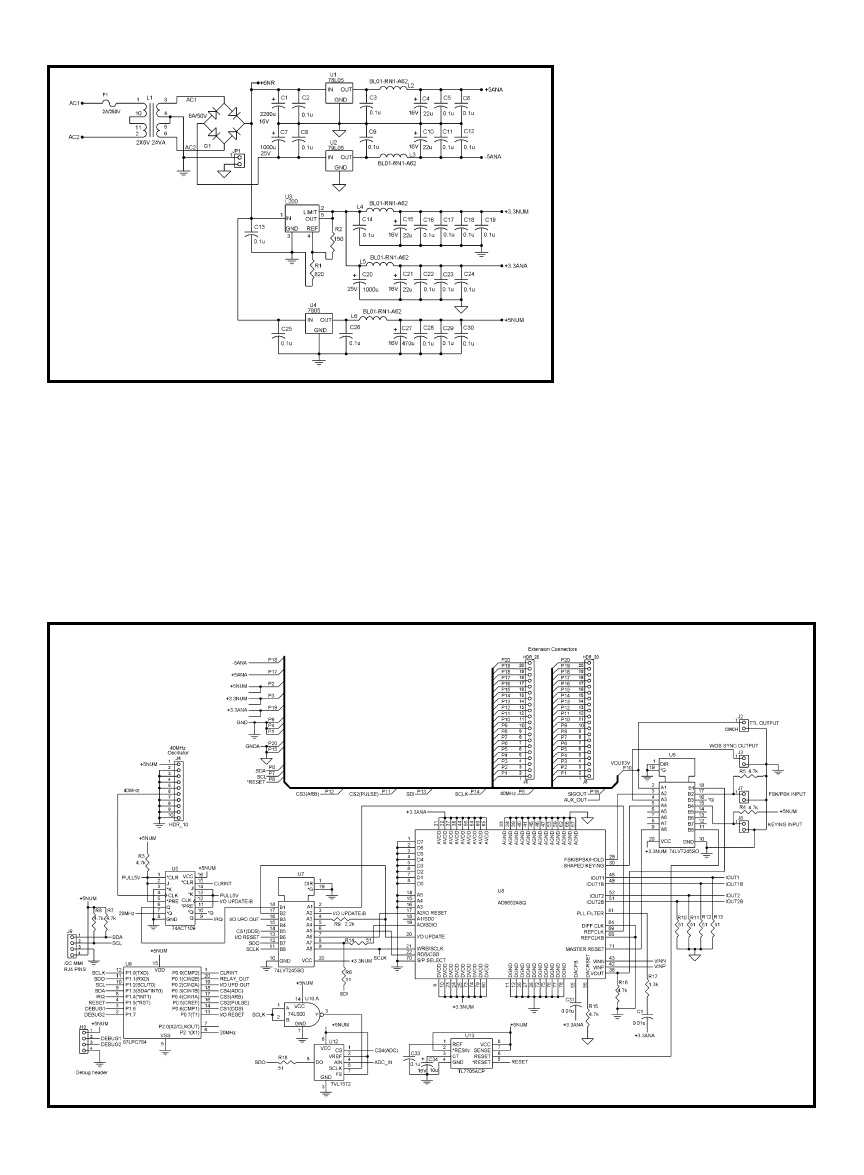
52
Issue 130 May 2001
CIRCUIT CELLAR
®
www.circuitcellar.com
generator. Then, there’s the Philips
87LPC764 serving as the main micro-
controller. And, the I
2
C-driven user
interface (described in Part 1, Circuit
Cellar
129). The next subsystem is
the A/D system that manages the
AM/FM/PM analog modulation input
(generated in software). And, the last
subsystem is the expansion connec-
tors for future plug-ins.
The power supply is not the sim-
plest part of this design (see Figure 4)
because of EMC/EMI constraints and
mixed 5-/3-V design. To minimize
noise on the analog output, separate
supplies are used for the 5-V digital
microcontroller, ±5-V analog output
amplifier, 3.3-V digital DDS chip and
buffers, and 3.3-V analog DDS chip.
Standard 78L05/79L05 regulators
are used for the ±5-V outputs, and a
reliable L200 (U3) is used for the 3.3-
V outputs. Filtering coils are inserted
in all power lines to minimize 300-
MHz cross-talk and separated ana-
log/digital grounds are implemented.
The DDS-GEN main system clock
is 20 MHz, derived from a standard
40-MHz canned oscillator and divided
by 2 by U5A to improve jitter per-
formance (see Figure 5). Its modest
stability (100 ppm) is enough for most
applications. However, the oscillator
is mounted on a plug-in PCB and can
be replaced easily by a high-perform-
ance, 40-MHz OVCXO, which would
boost the stability to 3 ppm (for a
price hike). The 20-MHz clock is mul-
tiplied by 15 thanks to the PLL inte-
grated in the DDS chip, giving a 300-
MHz system clock.
The AD9852 is serially controlled
by the microcontroller with an SPI-
compatible interface through a 5-to-
3.3-V level converter. The I/O update
signal is used as an interrupt source
to the microcontroller. This enables
you to synchronize the firmware with
the DDS chip operation. The pulse is
captured by a fast JK register
(74ACT109), because it’s only eight
clock pulses long at 300 MHz. And, it
has a 300-MHz internal clock fre-
quency that enables you to synchro-
Figure 4—
The DDS-GEN power
supply isn’t the easiest part of the
design. Both 5- and 3.3-V sources,
dedicated logic, and analog outputs
are needed. High-frequency decou-
pling is necessary to minimize the
300-MHz cross-talk.
Figure 5—
Here’s the logic. There
aren’t many components around the
87LPC764 and AD9852 chips. A pair
of LVT buffers is used for the 3.3-to-
5-V interface.
www.saelig.com • saelig@aol.com
English for happy, prosperous &
blessed -- which is what I want my
customers to be!) to bring unique,
easy-to-use control and instrumenta-
tion products to USA from Europe.
• Over 50 different DIN-modules for:
analog i/p & o/p, thermocouple i/p,
digital i/p, relays, on 2000m network!
9pin > 9pin . . . . . . . . . . .
self-powered . . . . . . . . .
digital data on
PC FlashATA cards
software function
modules—finish quickly.
RS232, interrupts, sleepmode,
pre-emptive multitasking, easy to
attach LCD or keypad.
• CANbus adapter—recompile or log
Self-contained in
2" x 3" plastic box,
logging/alarm system
standalone or with PC.
see what’s new at www.saelig.com!
Industry-standard
card for PC’s
• Master, Slave or Bus monitor
• Low volt ICA93LV for 3V ic’s . .
power & information on 2-wires!
Boards for PCI/ISA/PCMCIA/PC104/VME/compPCI
Drivers for WIn95/98/NT,VxWORKS, pSOS, Lynx,
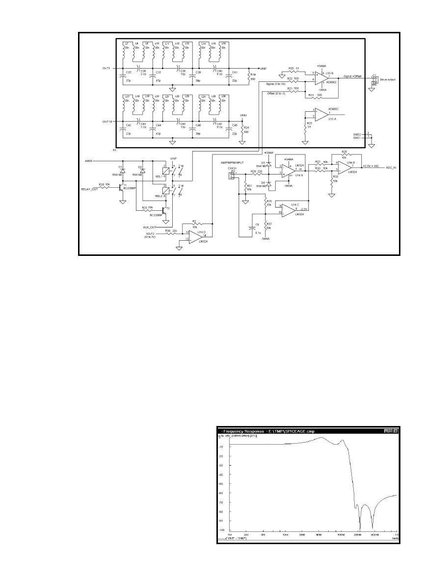
54
Issue 130 May 2001
CIRCUIT CELLAR
®
www.circuitcellar.com
nize the micro-
controller with
the DDS chip.
The TTL I/O
signals (Keying,
Square Output,
FSK/PSK, and
so on) are
buffered and
shifted to stan-
dard TTL levels
by Philips’
74LVT245 (U6).
These 3.3-V
transceivers
have 5-V, TTL-
compatible I/O
signals and an
impressive 2.4-
ns propagation
delay. Last but
not least, a
small
TL7705ACP pro-
vides a clean
reset pulse to
the DDS chip and microcontroller.
The main microcontroller is an
87LPC764, interfaced to the DDS chip
through 5-to-3.3-V converters. For
more information, check out the
datasheet. [2] The microcontroller is
clocked from the main 20-MHz sys-
tem clock. Its I
2
C port is used to con-
trol the user interface and plug-in
boards. The UART is configured as an
SPI controller, and drives the DDS,
external A/D converter, and plug-in
boards with distinct chip selects.
The last part of the design is the
analog stuff (see Figure 6), which is
the difficult part for firmware-orient-
ed types. To work with frequencies
above 100 MHz you need experience.
First of all, each complementary
output of the main DAC is fed
through a passive 120-MHz elliptic
filter to get out of the band frequen-
cies. I borrowed the filter design from
Analog Devices. [1] I modified the coil
values to be integer multiples of a sin-
gle value (just try to buy eight differ-
ent SMD coil values in small quanti-
ties and you’ll understand why I did it
that way). I checked the frequency
response, which still looked good (see
Photo 1). The two complementary
and filtered sine waves go back to the
AD9852’s internal high-speed com-
parator to generate the square output.
For the analog output, a pair of
high-frequency relays selects either
the sinus output (one of the two fil-
tered signals from the AD9852 DACs)
or the output of one of the plug-ins’
slots. The selected signal is amplified
and DC is offset by an AD8002 high-
speed current amplifier.
This amplifier has a gain bandwidth
of 600 MHz at –3 dB and provides 0.1-
dB flatness from 0 to 60 MHz. That
isn’t perfect for this application, but
it’s a good performance versus price
trade-off. Moreover, the 1200-V/µs
slew rate makes it adequate for your
pulse generator applications.
Last, the exter-
nal modulation
input (used for
AM/FM/PM
modes) is first
scaled and DC off-
set by a standard
LM324 (U14) in order to give a 0- to
5-V signal from the ±5-V input. This
signal is then fed into a small TI
TLV1572. This 10-bit A/D converter
is serially connected to the microcon-
troller through the shared SPI bus.
PROTOTYPE CONSTRUCTION
All but the user interface fits on a
7.4
″
× 6.7
″,
double-sided PCB, includ-
ing the power supply and its trans-
former (see Photo 2). The user inter-
face is mounted behind the front
panel. The high-frequency analog
parts are EMC-protected by a metallic
can (see Photo 3).
In order to maximize performance,
all high-frequency components are
Photo 1—
A simulation of
the transfer function of the
150-MHz low-pass filter
shows a 70-dB rejection
above cutoff frequency. This
simulation was done using
SpiceAge software.
Figure 6—
In the analog section, two
150-MHz elliptic passive filters elimi-
nate unwanted harmonics from the
DDS chip outputs. A pair of high-fre-
quency relays selects the relevant sig-
nal and directs it to an integrated high-
frequency amplifier (AD8002).

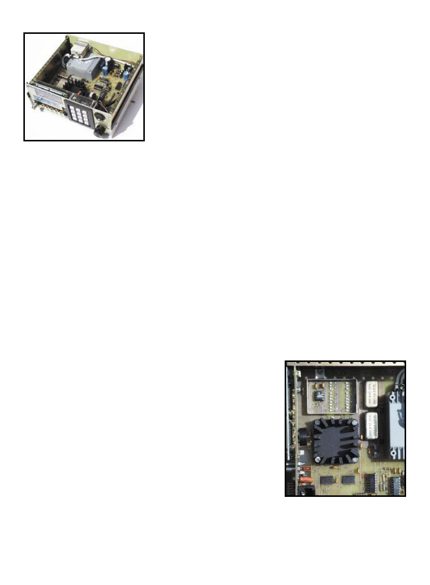
56
Issue 130 May 2001
CIRCUIT CELLAR
®
www.circuitcellar.com
Photo 2—
The DDS-GEN prototype shows that the
I
2
C-MMI board is behind the front panel. The main
transformer and filtered power plug are in the back.
The power supply components are in the back right
corner and the plug-in slots are visible in the front right
corner. The high-frequency parts are to the left
between the front panel plugs and transformer.
surface-mounted. And, a large ground
plane is integrated on both sides of
the PCB (an analog ground plane on
the topside for the HF areas and a dig-
ital ground plane on the bottom for
the digital parts). But, a full four-layer
PCB is a must. A metallic enclosure
and a filtering power socket are also
mandatory to limit the spurious emis-
sions and meet UL/CE specifications.
ON THE SOFTWARE SIDE
The complete listing of DDS-GEN
software is on the Circuit Cellar web
site. Like the I
2
C-MMI software, this
code is mainly written in C, thanks
again to the good freeware SDCC-
optimizing cross-compiler. Some in-
line assembler code is used, however,
mainly for interrupt handling routines
and code-space optimization.
And, as always, I check the Internet
to see if what I need is already out
there. I used, without modification,
the C code I
2
C handler library written
by Sandeep Dutta (thanks, Sandeep!)
and interrupt-handling code from the
SDCC accompanying files. [3]
The dynamic structure of the DDS-
GEN embedded software is classic
(field-proven) and interrupt-driven (see
Figure 7). After initializations, the
main program manages the user inter-
face and stores all parameters that
need to be loaded into the DDS chip
in a shared RAM buffer.
The interrupt routine, executed
each time the DDS chip asks for new
values with its “I/O update” signal,
executes an A/D conversion of the
external modulation signal. And if a
modulation is requested, it recalcu-
lates the frequency, amplitude, and
phase on the fly. It then uploads the
modified parameters into the DDS
chip one block at a time to limit
interrupt latency.
In order to define a precise interrupt
frequency, the DDS chip is pro-
grammed in Internal Update mode. In
Internal Update mode, the update of
its internal registers is automatic and
executed at a preprogrammed refresh
rate. The I/O update signal is an out-
put that generates an interrupt on the
microcontroller.
The shared RAM buffer maps exact-
ly the AD9852 register set. This array
is then segmented in blocks, corre-
sponding to the AD9852 serial trans-
fer blocks; each block is the set of
parameters that should be down-
loaded in one individual operation.
Every time a parameter change is
needed, the relevant registers are
updated by the main program in the
shadow array and a flag is sent to
indicate that the corresponding block
must be downloaded to the DDS chip
during the next interrupt.
DDS-GEN menus are managed by
a generic software menu engine,
which is based on a table of menu
targets stored in ROM. Each menu
target corresponds to a specific LCD
mask, and defines the static text to
be displayed and the numerical for-
mat of the value to be edited (num-
ber of digits before and after the dec-
imal). Each menu target also defines
a pointer to a pre-processing proce-
dure (
func_enterxxx). This procedure
is usually in charge of converting
the value to be edited from internal
to human form.
And, lastly, it defines a pointer to
a post-processing procedure
(
func_selectxxx). This procedure
usually controls conversion of the
value just edited from human to
internal form and updates the shad-
ow DDS parameter array in RAM.
The main menu engine is straight-
forward. Thanks to the onboard
intelligence of the I
2
C-MMI periph-
eral module, every value displayed
can be modified with the keyboard,
rotary encoder, or from a host com-
puter connected to the serial port
without specific code in the applica-
tion software.
DESIGN METHODOLOGY
As I explained in Part 1 last month,
I prefer spending time doing simula-
tion steps rather than burning a zil-
lion OTP chips. In order to get the
DDS-GEN working as quickly as pos-
sible, I settled on the following four
development steps:
Step 1: The full main program was
developed and simulated on my PC
under Bill’s classic Visual C++ envi-
ronment. The I
2
C-MMI peripheral was
fully simulated with software rou-
tines and the shadow DDS register
parameters were displayed with the
debugger as required. This step
allowed me to debug all of the user
interface and menu software (80% of
the total code) without having to get
onto the target chip;
Step 2: An emulation of the inter-
rupt handling code was developed in
C, and the target DDS chip was con-
nected to the PC through a hacked
LPT parallel port. This step was like a
homemade ICE (on the hardware side,
no more than a DB25-to-87LPC764
socket and some C lines), and allowed
me to fully debug the DDS chip regis-
ter issues (register mapping, trunca-
tion errors, etc.);
Photo 3—
The AD9852 is under the big heatsink, a
converted TO3. The shield that holds the two high-fre-
quency filters (with their 20 CMS coils) and the AD8002
amplifier are on the top side. On the bottom, you can
see the two 74LVT245 buffers and the 87LPC764. The
two metallic components left of the transformer are the
high-frequency relays.


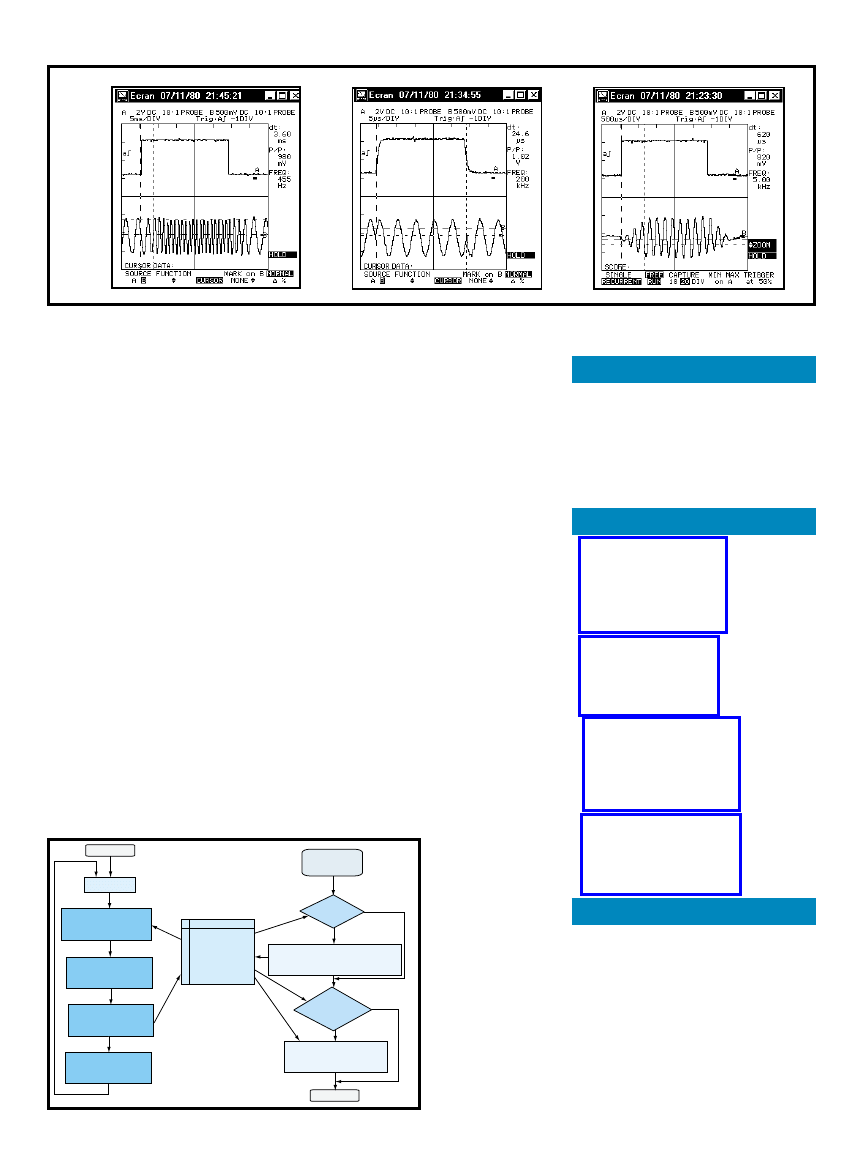
Robert Lacoste lives near Paris,
France. He has 10 years of experience
in real-time software, embedded sys-
tem developments, and now business
management. He still loves building
innovative, microcontroller-based
devices after hours. Currently, he
works for Nortel Networks. You can
reach him at robert_lacoste@yahoo.fr.
www.circuitcellar.com
CIRCUIT CELLAR
®
Issue 130 May 2001
59
Step 3: The specific target code was
added (mainly I
2
C-related stuff), the
interrupt routine was optimized, and
everything was cross-compiled to the
target 87LPC764. Then, everything
was debugged on the target;
Step 4: This step wasn’t planned,
but I had a memory space issue. The
first cross compilation ended with a
RAM and ROM requirement about
twice as large as 87LPC764 chip capa-
bility. A full iteration from Step 1 and
a lot of simplifications and optimiza-
tion were needed.
WHAT’S NEXT?
It wasn’t easy, but the DDS-GEN
prototype works (see Photo 4). The
hardware worked 99% flawlessly dur-
ing the first run, even if I still have
HF unwanted cross-talk and occasion-
ally a microcontroller randomly resets
at HF output. A new four-layer PCB
probably will be required to solve
them. The software still needs work,
mainly on the AM/FM/PM code,
which is crude because of lacking
space. And, I still have a list of left-
over bugs taped on the prototype.
Soon, I want to build an arbitrary
signal generator plug-in that will dra-
matically extend the possibilities of
the DDS-GEN. Basically, this board
will include another 87LPC764, I
2
C
EEPROM to store waveforms, cache
RAM chip, some kind of EPLD, and a
DAC. I also have firmware extensions
in mind, like an integrated, 1-kHz
pseudo-sinus modulation generator.
Well, I have some interesting nights
ahead, unless Circuit Cellar readers
want to take over part of the job…
I
Start
Initialization
Display current
menu entry and value
Wait for a user
action (new value)
Update DDS
parameters
Select the new
menu entry
DDS
parameter
and current
mode
I/O Update
interrupt
Modulation?
Get an ADC value
and calculate new
frequency, amplitude, and phase
New DDS
parameters?
Download first modified
parameter block to DDS
RTI
No
No
Photo 4—
The DDS-GEN generated these examples.
(a)
is a ramped 300- to 1200-Hz FSK signal with a 3.6-ms ramp time.
(b)
is a 200-kHz signal with 90° PSK modulation.
Finally,
(c)
is a 5-kHz signal in Shaped Keying mode with a 0.6-ms ramp up/down delay.
Figure 7—
A main program
waits for a user event, man-
ages menus, and updates a
parameter array in shared
memory. And, an interrupt
routine refreshes the DDS
chip registers and manages
modulation tasks.
a)
b)
c)
REFERENCES
[1] Analog Devices, Inc., “CMOS
300 MSPS Complete-DDS,” 1999.
[2] Philips Semiconductors, “Low
power, low price, low pin count
(20 pin) microcontroller with 4
kbyte OTP,” January 8, 2001.
[3] S. Dutta, “Anatomy of a
Compiler: A Retargetable ANSI-C
Compiler,” Circuit Cellar 121,
August 2000.
SOURCES
AD9852
Analog Devices, Inc.
(800) 262-5643
(781) 329-4700
www.analog.com
Visual C++
Microsoft Corp.
(425) 882-8080
www.microsoft.com
87LPC764, 74LVT245
Philips Semiconductors
(212) 536-0500
Fax: (212) 536-0559
www.philips.com
TL7705ACP, TLV1572
Texas Instruments, Inc.
(800) 336-5236
www.ti.com
SOFTWARE
The source code is available on the
Circuit Cellar
web site. This code is
copyrighted but can be used freely
without any guarantee, as long as
it’s not included in any commercial-
ly sold product.

60
Issue 130 May 2001
CIRCUIT CELLAR
®
www.circuitcellar.com
hen designing a
control algorithm
and analyzing its per-
formance, it is often
helpful to develop a software simula-
tion of the plant. The usual method is
to describe the plant by a set of first-
and second-order differential equa-
tions that are translated to discrete
time difference equations and solved
iteratively. These equations are usual-
ly based on idealized rather than real-
world physical behavior. It is possible
(but difficult) to model nonideal real-
world effects mathematically, but at
the cost of greatly increasing the com-
plexity of the model.
Another simulation method you
can use is to develop a behavioral
model of the plant. In this type of
model, the physical states of the sys-
tem’s components and resulting
behavior are directly represented and
computed iteratively at discrete time
increments, or time slices.
It is simple to modify the simula-
tion for different component charac-
teristics and nonideal effects to chal-
lenge the robustness of the controller
algorithm. You’ll find that it is also
simple to model mechanical and elec-
trical fault conditions. A stuck valve,
empty tank, or incorrect flowmeter
measurement can be easily simulated
to test the controlling software’s fault
handling.
The example I present here is a
simple fluid rate control system con-
sisting of a pump or pressurized tank
and a fluid line with a control valve,
cutoff valve, and flowmeter (see
Figure 1). The intent of this article is
not to show how to design a con-
troller for such a system, but to
demonstrate some of the techniques
and concepts of behavioral simulation
using this system as an example.
GENERAL SIMULATION
PRINCIPLES
Any computer-based simulation of
physical behavior is necessarily a dis-
crete time, discrete value approxima-
tion of a continuous time, real value
process, so unavoidably there will be
sources of inaccuracy in the simula-
tion. The first source of error is
numerical—the round-off and quanti-
zation error caused by using discrete
(not necessarily integer) numbers to
represent physical quantities.
Another source of error comes from
approximating physical continuous
time behavior with discrete time
models. It is a tacit assumption that
the physical process being approxi-
mated linearly interpolates between
two simulation times. (Interpolation
doesn’t have to be linear, but that’s
the simplest way.) That assumption
will not be correct to an infinite level
of precision, but the error can be
reduced to a negligible amount with
the appropriate time increment.
A more pernicious source of error is
what is known in chaos theory as sen-
sitive dependence on initial condi-
tions. In a complex set of higher order
nonlinear difference equations, two
slightly different initial conditions
lead to divergent results in the future,
and both diverge from the physical
process they represent. This prevents
the three-body gravitational problem
from being solvable numerically for
an arbitrarily long length of time, and
also makes weather impossible to pre-
dict more than a few days in advance.
In the types of systems normally
controlled by embedded processors or
simple control algorithms, mathemat-
FEATURE
ARTICLE
Simulation can be a
great tool for analyz-
ing performance.
However, unless you
follow some basic
principles, your model
can become too sim-
ple to reflect real-
world behaviors or too
complex to be practi-
cal. As youll see,
somewhere in
between is just right.
Kenneth Baker
Behavioral Plant
Simulation for Testing a
Control Algorithm
w
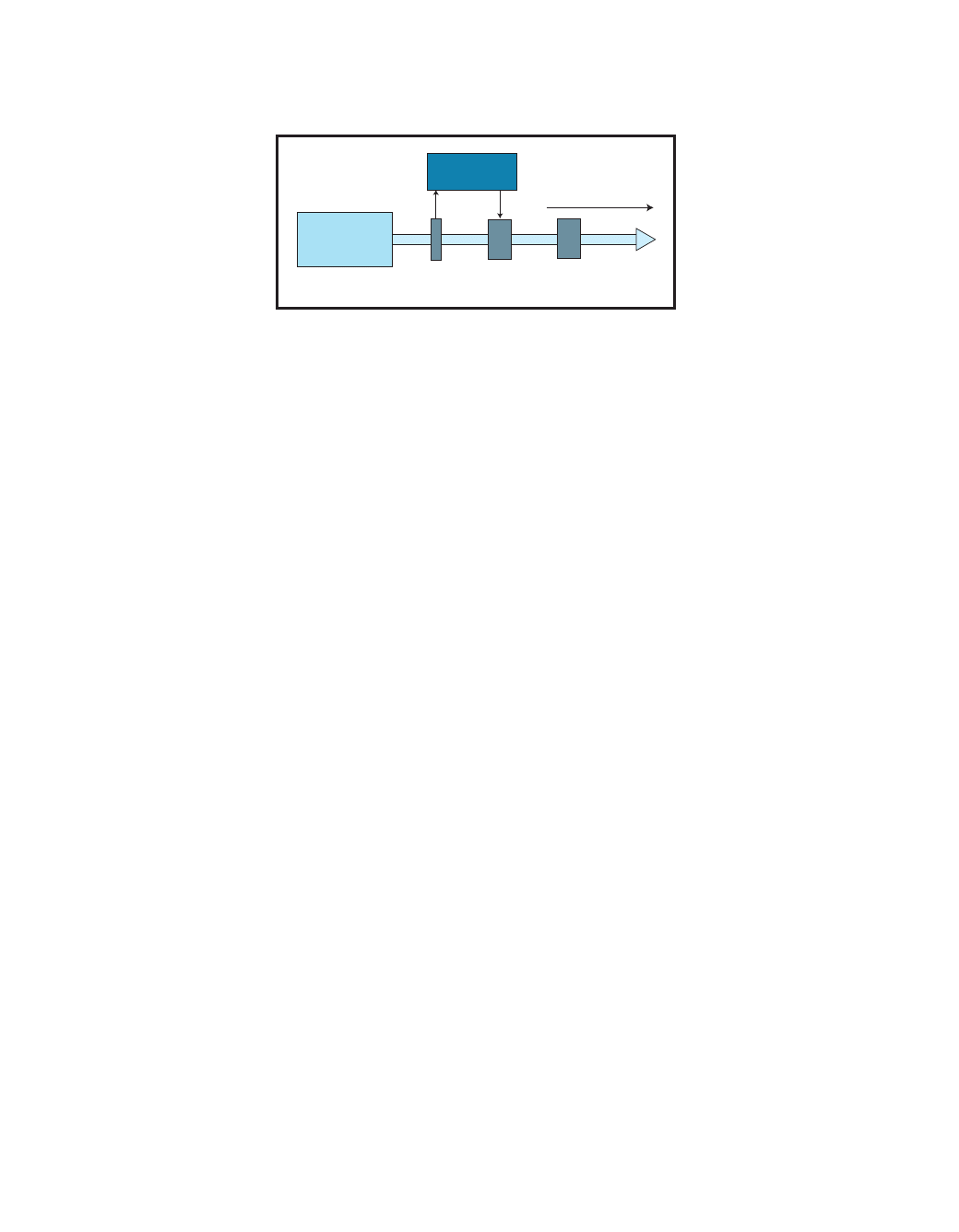
www.circuitcellar.com
CIRCUIT CELLAR
®
Issue 130 May 2001
61
ical chaotic behavior
isn’t a problem unless
the controller fails to
control. However, in a
large, complex system
with many compo-
nents, such as a large
automated manufac-
turing process or
power grid, it may
become a problem.
These systems require
far more sophisticated
simulation techniques
and are, as we have
read so often in textbooks and jour-
nals, beyond the scope of this article.
The first two questions to be
addressed are: How should physical
variables be represented and what
should the simulation time increment
be? A non-real-time simulation is not
computationally constrained by exe-
cution time and processor power, as is
often the case with an embedded con-
trol algorithm. Therefore, you are free
to use any data types and mathemati-
cal functions available.
Physical phenomena typically do
not take integer values, so the obvi-
ous choice is to use floating point for
all variables representing physical
states. Single precision is probably
sufficient for most cases to reduce the
quantization and round-off errors to a
negligible amount.
In order to minimize the time quan-
tization error the time increment
should be smaller than both the
shortest time constants in the system
and the sample period of the control
algorithm. In the system described
here, the time constants are in the
order of hundreds of milliseconds and
the controller sample period will be
100 ms. A simulation time increment
of 1 ms is two orders of magnitude
smaller so it’s a good choice.
In the following sections, I will
describe the simulation algorithms for
the individual components and then
show you how they piece together
and link to the control algorithm.
THE CONTROL VALVE
The rate control valve is the most
complex component with respect to
simulation in this system. In this
simulation, the valve is assumed to be
a butterfly valve with mechanical
stops at the fully open and fully
closed positions with 90° of motion.
The valve motor controls are PWM
DC signals that turn the valve plate
one way or the other at a constant
speed. At fully open, the plate is par-
allel to the pipe. A cross section of
the valve is shown in Figure 2.
The plate has to turn a few degrees
from the fully closed position before
an orifice opens. If the plate turns less
than this, fluid flow stops except for a
small amount of leakage caused by an
imperfect control valve seal. Two
other minor effects to note are the
starting and stopping delays for the
plate motion.
When power is applied it usually
takes a few milliseconds before
motion actually starts. Likewise,
when power is removed, inertia keeps
the valve moving for a few more mil-
liseconds. These two effects can be
important if the controller is trying to
make fine adjustments with short
pulses. For example, if the power
pulse is too short, the valve may not
move at all or the inertia may make it
move a little too far.
Valve motion is simulated by func-
tion
sim_valve() found in file valve.c.
The parameters of this function are
the valve number, or id, and the con-
trol command. The control command
tells the valve to open, close, or stop.
All of the local state and parameter
variables in file
valve.c are arrays
that the valve number indexes into.
This allows one function to simulate
any number of similar valves, which
have the same general properties but
may have different
characteristics and,
more importantly, can
be in different states. In
this project, I’m using
the same function to
simulate both the con-
trol valve and the shut-
off valve even though
they have different
characteristics.
The logical structure
of
sim_valve() is sim-
ple. It is to be called at
each time slice for each
valve, and it opens, closes, or stops
the valve, depending on the control
parameter and whether it needs to
delay or has a fault. The amount it
turns is defined by the valve rotation
parameter
prm_valve_rotation. This
parameter indicates how many
degrees the valve plate turns in one
time slice. If a valve takes 750 ms to
turn 90° from fully closed to fully
open or vice versa and the time slice
is 1 ms, then the valve rotation is
90
°/750 ms, or 0.12° ms. In this simu-
lation, the valve opens and closes at
the same speed. But, that doesn’t have
to be the case; the function easily can
be modified to provide separate
parameters for each direction.
After the valve plate position is set,
the resulting valve orifice is calculat-
ed. Because there are no assumptions
about the size of the valve at this
point, the orifice value is normalized
to 1.0 at the fully open position. At
some point during the simulation,
this normalized value (and others
described later) will have to relate to
an actual physical value. That will
come together when the simulation is
integrated with the control algorithm.
The calculation of the orifice is
based on the geometry of the valve, as
shown in Figure 2. Some valves have
a small amount of leakage when the
valve is nearly closed, and this leak-
age is represented as a fraction of the
normalized fully open orifice.
The important point here is not the
exact area of the valve opening at a
particular valve position. Rather, it is
the fact that the orifice, and thus flow
rate, are nonlinear functions of the
valve position. Some types of valves
Fluid flow
Pump or
pressurized
tank
Flowmeter
Control
valve
Cutoff
valve
Nozzle
Controller
Figure 1In a simple fluid dispensing system, the flowmeter and a control valve close the feed-
back loop with the controller. The cutoff valve operates in Switching mode, either fully open or
closed with no leakage.

62
Issue 130 May 2001
CIRCUIT CELLAR
®
www.circuitcellar.com
are more linear and others,
such as ball valves, are high-
ly nonlinear. Consequently,
a control algorithm that
assumes a linear plant
response will control with
different degrees of effective-
ness depending on the valve
position.
In this model, it appears
that many assumptions
about general behavior and
estimates of likely parame-
ter values were tossed out
without validation, but the general
behavior is justifiable on physical
principles. Typical valves do indeed
rotate at nearly constant speeds. Valve
motion cannot start nor stop instanta-
neously because of friction, momen-
tum, or capacitive and inductive
delays in the motor windings.
As for the parameter values, none of
the valve characteristics in this model
need to be known exactly for the sim-
ulation to be useful. Obviously closer
is better. If you have good ballpark
estimates, many simulations are exe-
cuted with different combinations and
ranges of parameters, and the control
algorithm is effective in simulation,
then you can be confident that the
algorithm will be robust enough to
perform acceptably regardless of the
physical parameters.
THE CUTOFF VALVE
The cutoff valve, as I stated earlier,
uses the same simulation code as the
control valve but with a different set
of parameters. Most importantly the
cutoff valve is assumed to have zero
leakage at the fully closed position,
otherwise it would be useless as a
cutoff valve.
A cutoff valve in a system like this
is also typically faster than the con-
trol valve. However, the cutoff valve
is nearly always fully open or closed,
so within limits the rotation speed is
not critical.
THE FLOWMETER
The flowmeter simulation is sim-
pler than the valve, but is not without
complications. It generates a pulse
train with a frequency proportional to
the fluid velocity. There are two non-
ideal effects modeled here. The first is
the response time. Flowmeters typi-
cally respond quickly to changes in
fluid velocity, but no flowmeter can
respond instantaneously. So, the fre-
quency at each time slice is modeled
as an auto-regressive function of the
previous frequency and the current
fluid velocity scaled by a constant:
f(t) = Awr(t) + (1 – w)f(t – 1)
where f is the frequency, A is a pro-
portionality constant between the
fluid velocity and frequency, and w is
the auto-regressive filter coefficient,
or weighing factor. A large value of w
means the current time slice is more
heavily weighted, causing the flow-
meter to respond faster to a change in
fluid velocity.
The flowmeter response is simulat-
ed by function
sim_flowmeter() in file
flowmtr.c. Like sim_valve(), this
function takes an identifier as a
parameter so that multiple flowme-
ters can be simulated with the same
code, but here only one is used.
The other parameter is the flow
rate, which represents the fluid veloc-
ity. Like the orifice in
sim_valve(),
this flow rate is assumed to be nor-
malized to 1.0 for a value that results
in a frequency numerically equal to
A
. And, this normalized value also
does not yet need to be related to a
physical value.
The second nonideal effect is
caused by both the temporal and
numeric quantization of the frequen-
cy measurement. In a typical embed-
ded system, the frequency of a pulse
train is measured by counting pulses
over a predetermined interval or by
measuring the interval
between two pulses (e.g.,
the pulse accumulator hard-
ware in the 68HC11 series
of microcontrollers).
The pulse accumulator
can either count external
pulses directly or, with the
addition of an external flip-
flip that toggles on every
pulse, can measure the
pulse interval in Gated
Time Accumulation mode.
Both of these functions are
included in
sim_flowmeter().
The problem is figuring out when
the pulses should occur. It is not as
easy as simply inverting the frequen-
cy. For example, if the gated counting
interval is 100 ms and the pulse fre-
quency is 333 Hz (i.e., an interval of
about 3 ms), then the counting period
may contain either 33 or 34 pulses.
This temporal quantization would
cause the calculated frequency to
alternate between 330 and 340 Hz, a
difference of about 3%. If the count-
ing interval were 20 ms, the calculat-
ed frequency would toggle between
300 and 350 Hz.
If this difference is too great for a
given application, a wise control engi-
neer would include some filtering of
the flow rate in the control algorithm
or increase the counting interval. The
tradeoff is increased controller
response time. This simulation would
allow you to determine the counting
interval or filter coefficients that
allow accuracy and response time
requirements to be met.
For the best simulation accuracy,
you have to calculate the times at
which pulses occur with greater preci-
sion than the simulation time incre-
ment. Greater precision is accom-
plished by accumulating the fraction
of the pulse-to-pulse interval that
accrues during each time slice, based
on the instantaneous frequency. For
example, if the current frequency is
200 Hz (5 ms between pulses) and the
time slice is 1 ms, then 20% of the
time between two pulses will elapse
in the current time slice. This incre-
ment is simply the time slice divided
by the pulse period, or in other words,
multiplied by the frequency.
Fully closed position
Fully open position
Minimum open position
θ
min
θ
d = cos(
θ
min
) – cos(
θ
)
Figure 2Check out the butterfly valve geometry and orifice calculation. The plate
rotates a few degrees from fully closed before it reaches the minimum open posi-
tion.
q
min
is the minimum open position,
q is the valve plate position, and d is the
normalized orifice.
1.888.941.2224 www.arcomcontrols.com
Your Embedded Controller SHOULD:
be industrial enough to survive even the harshest environments
have long term availability and support
be reliable enough for continuous operation
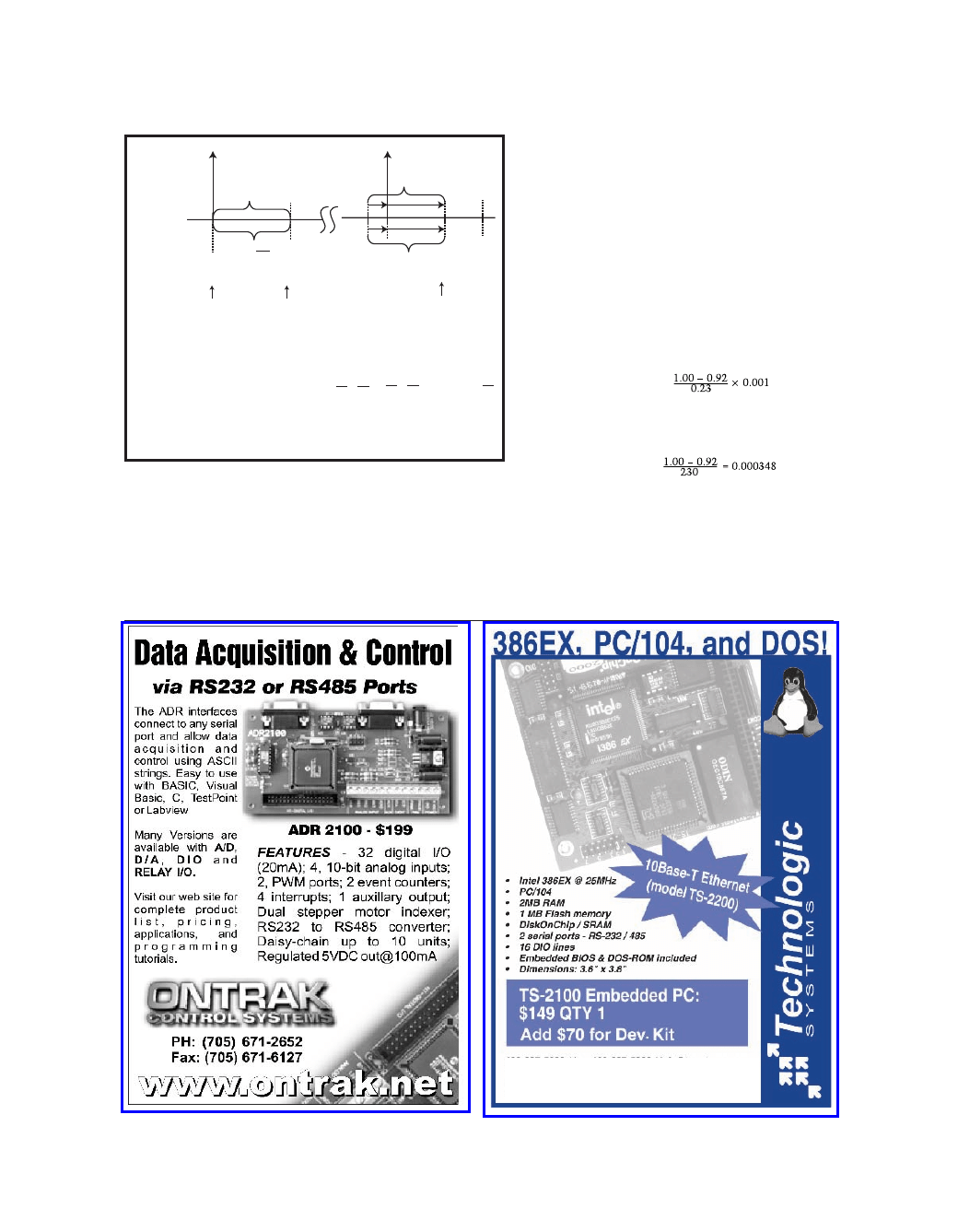
64
Issue 130 May 2001
CIRCUIT CELLAR
®
www.circuitcellar.com
This increment is accumulated
until it exceeds 1.0, and concurrently
the elapsed time since the last pulse
is accumulated. When the accumulat-
ed increment exceeds 1.0, it indicates
that a pulse has occurred. Exactly
when the pulse occurred is the accu-
mulated time plus the portion of the
time slice between the previous accu-
mulated increment and 1.0. This con-
cept is confusing even to this humble
author, so I’ll try to make it more
understandable with a concrete
numerical example.
Assume for simplicity a constant
frequency of 230 Hz and a time slice
of 1 ms. During each time slice, the
increment between pulses advances
by 0.23, or 23%, of the way from the
last pulse to the next. After 4 ms, the
accumulated increment is 0.92.
During the next time slice, the accu-
mulated increment advances to 1.15,
meaning a pulse occurred. The exact
time the pulse occurred is calculated
geometrically, as shown in Figure 3,
by:
which is the same as
This time is added to the accumu-
lated time of 0.004 to get 0.004348,
which is the period of 230 Hz. Now,
because the pulse occurred some time
before the current simulation time,
the pulse-to-pulse increment and
Figure 3For
accurate pulse
interval simulation,
flowmeter pulses
may not occur
exactly at the sim-
ulation time slices,
so the pulse times
must be interpo-
lated between
time slices. Right
here, the pulse
frequency (F) is
230 Hz, period (P)
is 1/F = 4.3478
ms, and the simu-
lation time slice
(T) is 1 ms.
t
1
t
2
i
1
i
2
T
I
A
B
C
T = 1 ms
0.00
0.23
0.92
1.00
0.15
0.38
0.0000
1.0000
4.0000
4.3478
0.6522
1.6522
I = T
P
= Tf
Pulse
Pulse
Accumulated
time (ms)
Accumulated
increment
between pulses
Time A: The first pulse occurs and accumulated time and increment are pre-loaded with 0.
Time B: At the next time slice, accumulated time advances by 1 ms and accumulated increment
advances by 0.23, or 23%, of the way to the next pulse.
Time C: At this time slice, accumulated increment advances to 1.15, indicating a pulse occurred.
The time of pulse is 4.000 + t
1
, which is calculated by
In this example, f = 230, i
1
= 1.00 – 0.92, and t
1
= 0.3478 ms. So the pulse occurs 4.3478 ms after
the previous pulse.
Now, the accumulated time is pre-loaded with t
2
= T – t
1
= 0.6522 and the accumulated increment
is pre-loaded with i
2
= I – i
1
= 0.15.
T
I
t
1
i
1
=
1
f
t
1
t
1
i
1
=
i
1
f
=
or
,which gives
.
66
Issue 130 May 2001
CIRCUIT CELLAR
®
www.circuitcellar.com
accumulated time must be pre-loaded
with values from the pulse that just
occurred to the current time slice so
that the next pulse-to-pulse interval
can be correctly calculated. In the
example used here, the increment is
pre-loaded with 1.15 – 1.00 = 0.15 and
the accumulated time is pre-loaded
with 0.001 – 0.000348 = 0.000652.
This may seem like a lot of work
for little value when the true frequen-
cy of a pulse stream is the inverse of
the period. However, if the controller
uses a poor choice of interval for
accumulating pulses, the results of
this temporal quantization will be
evident in the simulation, and the
problem can be addressed.
One thing to note here is that the
pulse accumulator in the 68HC11 is
only 8 bits, yet this simulation deals
with values larger than 255 bits. How
does this work? The assumption is
that there is an interrupt handler
behind the scenes that correctly han-
dles the pulse accumulator overflow
interrupt and uses it to construct val-
ues larger than 8 bits.
PLANT SIMULATION
The plant simulation is where all of
the component simulations come
together. Function
plant_simulate()
in file
plant.c calls functions to simu-
late the flowmeter, both valves, and
the PWM power supplies for each
valve. The latter behaves like typical
PWM outputs provided on a micro-
controller such as the 68HC11.
plant_simulate() also calls a function
to simulate to fluid flow rate.
All of the component simulations
for a given time slice conceptually
take place simultaneously. Obviously,
they take place sequentially in any
nonconcurrent computer simulation,
so the order in which they occur may
be important. The principle for deter-
mining the order is that a physical
system can’t respond instantaneously
to changing stimuli. This means the
flowmeter does not respond instanta-
neously to flow rate, and the flow rate
does not respond instantaneously to
valve position.
Consequently, the flowmeter must
be simulated before the flow rate is
recalculated so that the current
flowmeter frequency is based on the
flow rate from the previous time slice.
Likewise, the flow rate must be recal-
culated before the valve motion is
simulated. Realistically, however,
when the time slice is several orders
of magnitude smaller than the time
constants of the system, things
change so insignificantly from one
time slice to the next that the order
makes little difference.
Another available approach is to
keep two sets of state variables, one
for the results of the current time
slice and one saved from the previous
time slice. Only the previous vari-
ables are used to calculate the current
results, so the order of simulation is
arbitrary. This is a more theoretically
correct approach, but the resulting
differences should be negligible for a
small time slice.
The flow rate calculation in func-
tion
calculate_flow_rate() is the link
between the valve and flowmeter sim-
ulations. The flow rate, or fluid veloc-
ity, is a function of the two valve ori-
To order, visit our web site or call
FREE! PCI Bus Quick Reference Guide
Visit
books and eBooks on embedded systems design,
wireless telecommunications, DSP, and more!
$49.95 print version
ISBN 1-878707-54-X
Includes CD-ROM

www.circuitcellar.com
CIRCUIT CELLAR
®
Issue 130 May 2001
67
fices and pressure. The pressure vari-
able represents the pressure of the
tank, or pump, feeding the fluid line.
But in this simulation, it is never
linked to a physical quantity because
it is neither measured nor influenced
by the controller.
A factor in the flow rate calculation
proportionately modifies the flow
rate. And, this can be used to make
the flow rate response change over
time. Like the valve orifices, pressure
and flow rate are normalized. When
both orifices are 1.0 and the pressure
is 1.0, the resulting normalized flow
rate is 1.0. For a given pressure, the
flow rate varies with valve orifice the
same way current through a resistor
varies with conductance.
Thus, the equation for fluid rate
through two valves takes the same
form as current through two series
resistors, using conductance rather
than resistance. The equation is
(without the noise term):
where r is the flow rate, p is the pres-
sure, and v
0
and v
1
are the valve ori-
fices. A factor of 2 normalizes r to 1
when p, v
0
, and v
1
all are 1. Note that
v
0
and v
1
are limited to 1 because the
valves can’t be more than fully open.
But, p is not limited to 1, and there-
fore f is not limited to 1.
A random (actually pseudo-random)
noise term is added to the flow rate
you just calculated. This represents
random variations in the flow rate
caused by turbulence, variations in
the pump output, transient obstruc-
tions at the nozzle, and so on.
During each control time, a new
random number is calculated and the
noise term between control times is
interpolated between each pair of ran-
dom numbers. This allows the ran-
domness to vary on a time scale that’s
significantly longer than the time
slice. This way the noise looks more
like turbulence rather than Brownian
motion. The amplitude of the noise
term is scaled to a percentage of the
full-scale flow rate using the constant
RAND_MAX provided along with the
pseudo-random function in the stan-
dard C library.
THE CONTROLLER
Function
control_rate() in file con-
trol.c implements a basic PID con-
trol algorithm and converts the con-
trol signal to a pulse width and direc-
tion for the control valve. This is
intended to be representative of an
algorithm that will be in an embedded
controller. This is where you can test
different algorithms, different varia-
tions of the same algorithm, different
control periods and parameters, fault
handling algorithms, and execute each
test algorithm with different plant
characteristics.
The control algorithm is also where
the normalized simulated physical
quantities finally get linked, although
still in an abstract way, to a physical
quantity. In function
control_rate(),
a call to
get_flowmeter_period()
returns the flowmeter period quan-
tized by a 31,250-Hz clock, which is a
typical clock rate for the gated time
accumulator in the 68HC11. This
quantized period is converted to a fre-
quency by:
where f is the frequency and P
q
is the
measured flowmeter period. The
clock frequency of 31,250 Hz is the
inverse of the flowmeter period reso-
lution set by a call to
set_flowmeter_parameters() in
plant_initialize(). This calculated
frequency is the actual rate, which is
compared to the target rate in the
control algorithm. How this frequen-
cy depends on the actual flow rate
depends on the size of the pipe and
response of the flowmeter.
Time (ms)
Event
Data
Description
50
Set P coefficient
Varies
Set the coefficients for the PID controller. In these scenarios, I and D are constant but P changes
Set I coefficient
0.001
to obtain different response times and overshoot. In scenarios 0, 1, and 2, P is 0.2, 1.0, and
Set D coefficient
0.005
1.8. In scenarios 3 and 4, P is fixed at 1.0 and the valve speed varies. In scenarios 4 and 6,
P is fixed at 0.2 and the valve delay compensation varies.
Set delay
Varies
Valve delay compensation is fixed at 10 ms for all scenarios except 5 and 6, which are 0 and 20
compensation
to test under and over compensation.
Set valve speed
Varies
The valve speed is fixed at 0.12°/ms, or 750 ms, for full motion, except scenarios 3 and 4, which
are 0.06 and 0.24 to test slower and faster valves.
150
Target rate
81
Step from 0 to the mid range
3600
Target rate
172
Step from mid to high rate
6400
Target rate
23
Step from high to low rate
9000
Set pressure
0.66
Reduced valve pressure, actual rate should drop
9050
Set valve fault
On
Valve is stuck in position
9100
Set flowmeter noise
0.15
Flowmeter noise amplitude increases to 15% of the current actual rate
10100
Target rate
141
New target rate, valve is still stuck, so theres no response
12200
Clear valve fault
Off
Valve is able to respond, but the pressure is too low for the target rate to be reached.
19100
Target rate
69
Mid-range target rate can be reached at a lower pressure
24000
Target rate
0
Full stop
25000
Set pressure
1.00
Nominal pressure and no noise to get a clear view of the step response time and overshoot. Both
Set flowmeter noise
0.0
low to high and high to low pressure.
26000
Target rate
150
Step from 0 to high rate
29000
Target rate
30
Step from high to low rate
32000
End simulation
0
Terminate program
Table 1To simulate a test protocol, a sequence of target rates is executed multiple times with varying controller parameters and plant characteristics to analyze the perform-
ance of the controller.
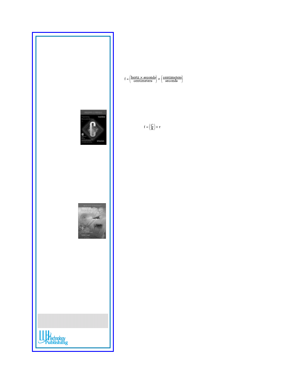
68
Issue 130 May 2001
CIRCUIT CELLAR
®
www.circuitcellar.com
Assume the cross-sectional area of
the pipe is Acm
2
and the response (f)
of the flowmeter is a constant (C)
multiplied by the fluid velocity (v).
The answer is given in hertz:
The flow volume (R) is the area
multiplied by velocity. So for a given
area (A) and flowmeter response (C),
the frequency corresponding to a
given flow volume (r) is
Ultimately it is this flow volume
that is being controlled using the
measured frequency as a proxy. You
set the target frequency for a desired
flow volume based on this equation,
but as far as the control algorithm is
concerned, the frequency is the only
important quantity, not the flow vol-
ume. This is why it is reasonable to
use normalized simulated quantities
for the flow rate and valve openings.
The constant, which is the flow coef-
ficient set in
set_flowmeter_parame-
ters() called by plant_initialize(),
indicates the frequency that will
result when both valves are fully
open. And it indicates that the fluid
pressure is at an arbitrary value that’s
normalized to 1.0 in the simulation.
THE TESTBENCH
The
main() function contains the
testbench where the plant simulation
is linked to the control algorithm
along with facilities for executing pre-
defined test scenarios and recording
the results. The logical structure of
the testbench is simple. It contains a
loop that represents 1 ms per itera-
tion. The plant simulation is called
once per iteration and the controller
is called once per control period,
which is a constant number of itera-
tions (in this case 100). Each time the
controller is called, the target and
actual rates are stored as text in a file
that can later be loaded into an appli-
cation such as Microsoft Excel and
graphed and processed to determine
response times and overshoot.
The testbench also has an event list
processor that reads data from an
event list in
ev_scen.h and uses that
data either to change the target rate or
a parameter in the plant or controller.
This provides a simple way to design
a set of repeatable tests that can be
executed against variations in the
control algorithm.
Each element of the event list is a
structure that contains the time at
which the event is scheduled to
occur, a code indicating what type of
event it is, and three different types of
data elements. The use of the data
elements is code-specific.
I designed seven simple test scenar-
ios that exercise the basic functionali-
ty of the plant and controller. You can
download these tests (file
EV_Scen.h)
and the results (labeled scenario zero
through six) from the Circuit Cellar
web site. All seven scenarios have the
same sequence of target rates, but
with varying controller parameters or
valve speed. The scenarios follow the
sequence of events shown in Table 1.
Scenarios 0, 1, and 2 vary the P
coefficient while other parameters are
held constant. In scenario 0, with a P
equal to 0.2, you see slow response
times and minimal overshoot in the
first several steps. At about 9 s, the
rate falls because of the pressure drop.
When the target rate jumps up again,
the response does not follow until the
valve is free; and then it isn’t able to
reach the target rate because of the
lower pressure. Also, by this time the
higher noise amplitude is evident.
The last two steps are pure step
responses with no noise or faults.
In scenario 1, P is 1.0, and you see
faster response times and only slight-
ly more overshoot. In scenario 2, with
P equal to 1.8, the response time is
about the same as for scenario 1 but
the overshoot is higher.
Scenarios 1, 3, and 4 hold P con-
stant at 1.0 and vary the valve speed.
Scenario 3 has a valve speed twice as
fast as scenario 1 and consequently
the overshoot is dramatically higher.
In scenario 4, the valve speed is half
as fast and the response is sluggish.
Scenarios 1, 5, and 6 hold P con-
stant at 0.2 and vary the valve delay
compensation. Scenario 5 has no
Programming Microcontrollers
in C, Second Edition
by Ted Van Sickle
ISBN 1-878707-57-4
For more info on this title and the
Embedded
Controller
Hardware Design
For more info on this title and author,
visit:
www.circuitcellar.com
CIRCUIT CELLAR
®
Issue 130 May 2001
69
delay compensation, so valve motion
is reduced and the response is more
sluggish. The valve compensation is
doubled in scenario 6, with results
similar to increasing P.
These are not the only useful
testable scenarios, or even the best.
This set of tests merely demonstrates
the method of varying one parameter
while holding all others constant in
order to isolate the effects of changing
a particular parameter.
CONCLUSION
If the system simulated here is
actually built and tested, it almost
certainly will not behave exactly like
the simulation. But the question is
whether or not the simulation is real-
istic and accurate enough to be useful.
A control valve obviously will have a
finite speed, will probably leak a little
when it is closed, and probably delay
or keep moving for a few milliseconds
when power is applied or removed.
Moreover, the flowmeter will respond
predictably to fluid velocity, other-
wise it is useless, and there probably
will be small stochastic variations in
the measured fluid flow rate.
If I test my control algorithm
against ranges of likely plant charac-
teristics, then when the system is
built, I should be able to pick a set of
control parameters from among the
test set that worked well the first
time. This may not eliminate, but at
least reduces the time and expense of
testing the controller on the system.
If it turns out that the valve or
flowmeter characteristics differ too
much from what I simulated, I deter-
mine the new characteristics (approxi-
mately). Then I go back to my simula-
tor and, perhaps with a different con-
trol period, execute a set of test sce-
narios again to find the control
parameters that work.
The control algorithm and test sce-
narios presented here are obviously
not the only meaningful choices. I can
imagine, for example, designing a con-
trol algorithm that measures response
time and overshoot and uses that
information to adjust the plant
parameters. In that case, you could
design a scenario that reduces pres-
sure either gradually or in steps while
the target rate steps up and down, to
see if the controller can adjust appro-
priately and maintain the same
response. A fault detection algorithm
could be designed to recognize when
the rate fails to respond and take
appropriate fault recovery action. This
type of simulation also could be used
to test experimental algorithms. For
example, a learning algorithm that
remembers how much valve motion
from a given position produces a
given rate, and uses that knowledge to
bypass the PID algorithm and move
the valve directly to the right place.
As I stated earlier, it’s not necessary
for this simulation to be exact to be
useful. The machinery won’t behave
exactly the same way twice. But if the
simulation is realistic and program-
mable, and an experimental control
algorithm is tested against likely
ranges of simulated characteristics
and meets requirements, then you can
be confident your control algorithm
will take control.
I
Kenneth Baker earned a B.S. in
Electrical Engineering from Illinois
Institute of Technology in 1985 and
an M.S. in Electrical Engineering from
University of Minnesota in 1993. He
has designed and programmed
embedded computers for various
industries including defense, agricul-
ture, traffic control, and medical.
Currently, he works for Guidant
Corp., a manufacturer of implantable
cardiac rhythm management devices.
You may reach him at martkenn
@megsinet.net.
SOURCES
68HC11
Motorola, Inc.
(847) 576-5000
Fax: (847) 576-5372
www.motorola.com
Excel
Microsoft Corp.
(425) 882-8080
www.microsoft.com
SOFTWARE
The code and seven simulation
graphs are available on the Circuit
Cellar
web site.

70
Issue 130 May 2001
CIRCUIT CELLAR
®
www.circuitcellar.com
f you’re like me,
you frequent your
local Radio Shack as
though it were a book-
store. I’m always in there checking
out what’s new. Remember when
they used to give away free flash-
lights? Radio Shack sold lots of batter-
ies through this successful marketing
move. Free isn’t a word you see used
much today, unless it’s an enticement
to subscribe to a long-term contract
for cell phones.
The days of freebies (i.e., no strings
attached) have returned. Radio Shack
has been handing out free scanning
devices from Digital:Convergence.
D:C believes that if it puts one of
these in the hands of every user, swip-
ing every bar code in sight will
become a simple alternative to key-
boarding your way through the infor-
mation superhighway. D:C’s bar code-
scanning :CueCat is capable of con-
necting you with an associated prod-
uct’s web site without as much as a
single keystroke.
The :CueCat is a mouse-sized bar
code-scanning wand shaped like a cat
who looks ready to pounce on those
unsuspecting zebra stripes. There is a
registration process you must go
through to unlock the :CRQ (see our
cue) software. This is used to link you
to the embedded serial number of
your :CueCat. Some people get nerv-
ous when they find they are being
checked for identification, but others
welcome the idea of having informa-
tion filtered to their preferences,
removing any unwanted fluff. In this
way, you get only the information
that interests you.
VISIT THE CAT
Radio Shack sells the :CueCat. Or,
you can find out where to get it for
free (there’s that word again), or have
one sent to your door for only the
shipping and handling fees at
www.:CueCat.com/getcat. html.
:CueCat was designed to look like a
keyboard to your PC. Its output is the
same format as the PC keyboard.
Each keystroke produces more than
just one byte of data. There are at
least three bytes sent each time you
hit a key. A key code is sent whenev-
er a key is pushed, and a break code
and key code are sent whenever a key
is released. To be compatible with the
keyboard, the :CueCat must send all
characters using this format. A suc-
cessful scan consists of five parts: pre-
fix, unique serial number, code type,
scan data, and suffix.
Each of the five parts of a :CueCat’s
transmission is separated by a period.
An <ALT F10> sequence is sent as a
prefix and a <CR> sequence is used as
a suffix. This leaves the middle three
groups as the actual data. If you take a
look at the PC’s key codes, all possi-
ble 8-bit bytes are not represented by
keys, so sending 8-bit data is not easi-
ly accomplished through using key-
strokes. One way to accomplish this
would be to send an 8-bit data byte as
two hexadecimal nibbles (0–9 and
A–F). To pack data more closely
together, D:C uses the lowest 6 bits of
each byte to send data (a–z, A–Z, 0–9,
and two characters). This format
requires four bytes (6 bits at a time) to
send three 8-bit data bytes, however,
D:C uses a simple XOR of each data
byte (with C) to further complicate or
encrypt the data.
Humans are a strange bunch.
Curiosity is one of the traits that has
allowed us to become dominant over
FROM THE
BENCH
Fact or
fiction—
nothing
is free
and the
Internet
is getting harder to
navigate. Jeff found a
device that’s freely
distributed and can
make navigating the
Internet as easy as
scanning a bar code.
Jeff Bachiochi
Taking a Cue from a Cat
Hardware Cleanup with :CueCat
i
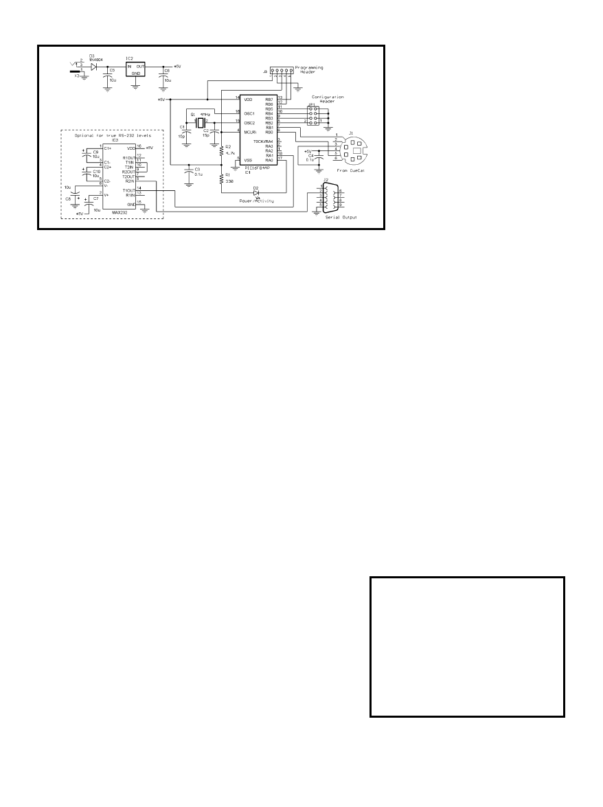
www.circuitcellar.com
CIRCUIT CELLAR
®
Issue 130 May 2001
71
other creatures. For every product
that is created, there are millions who
will use it for its intended purpose.
There are also a bunch who wonder,
“How’d they do that?” Out of this
group, some will grab their screw-
drivers based on the need to find out
how it was actually done. It still
amazes me how quickly this last
group shares their findings with oth-
ers who have the same interests. For
the most part, this crowd is not in it
to prevent marketing companies from
obtaining the fruits of their labors.
Bar coding is on all kinds of prod-
ucts now. Bar codes provide vendors
with a way to control inventories.
Checkout lines are automated using
product pricing information. Letters
and packages are routed via bar cod-
ing. It only makes sense that we use
these markings to make our daily
lives easier.
There are a few approaches you can
take to use the :CueCat for other
applications. You can alter the
:CueCat to output data in a more
usable format. You can write a driver
program to translate the :CueCat’s
data into a more usable format, or you
can use a black box to accept the
:CueCat’s keyboard codes and trans-
late them directly into usable data.
I opted for the last choice for a
number of reasons. I didn’t want to
prevent the :CueCat from being used
as it was intended. In translating the
:CueCat’s output into universal serial
transmissions (9600 bps), it can be
used as input to many different types
of equipment, including PCs, PDAs,
or embedded systems.
CAT’S BOX
Using a hunk of hardware to per-
form :CueCat translation may not
seem cost-effective, but this is not an
expensive approach. The cat’s box
schematic in Figure 1 shows what
was used to complete this task. This
circuit’s PS-2 mini din receptacle
mates with the :CueCat’s keyboard
connector and supplies 5-V power to
the :CueCat. The remaining signals
(besides the power and ground) are
reset, clock, and data. These are all
TTL-level signals and do not require
any level conversions. The clock and
data lines are open-collector outputs
from the keyboard (cat) and inputs to
the microprocessor (the keyboard is
normally in charge of handling these).
The microprocessor can request a
wait state by pulling the clock line
low if it requires processing
time in-between the reception
of characters.
At the Other end of the Cat’s
box, a DB9 outputs asynchro-
nous data to any serial port.
The RS-232 signals should have
a positive/negative voltage
swing. Most PCs will accept a
TTL-level signal. I’ve designed
the microprocessor to output an
inverted serial format, which
presents the format normally
seen at an RS-232 connection.
The MAX232 in the schematic
is used to invert the signal
twice and present RS-232 levels (in
place of the TTL levels) if needed.
The LED was originally put on to
indicate when the :CueCat was send-
ing a transmission, however I inverted
its function so that it acts as a power
LED, turning off briefly when it sees a
transmission. Configuration jumpers
allow you to eliminate any of the
:CueCat’s output functions—serial
number, code type, or bar data. A
forth jumper enables the raw output
to be sent out the serial port for
debugging purposes.
CAT’S KEYBOARD EMULATION
To look like a PC keyboard, the
:CueCat must emulate the output of
the keyboard. A PC’s keyboard trans-
mission consists of a clock and data
line. Data is available to be read from
the keyboard on each of the clock
line’s falling edges. To indicate the
beginning of a transmission, the data
line must be low on the clock’s first
falling edge (i.e., the start bit). The
next eight falling edges of the clock
line indicate keyboard data (LSB to
MSB). Following the eight data bits,
an odd parity bit is sent. This gives a
small amount of insurance that the
data was received correctly. Finally,
the data line must be high for the
next falling edge (stop bits).
As I stated earlier, a minimum of
three data bytes are sent for each key-
stroke. A character code is sent while
you press a key, and a release code
and character code are sent when you
release the key. When the release code
F0 (240-decimal) precedes a character
code, it indicates that the character
Keyboard codes received from :CueCat (hex):
12 21 F0 21 F0 12 26 F0 26
31 F0 31
1A F0 1A
Four bytes of character data translated from keyboard codes (hex):
C 3
n
z
Look-up translation (6-bits):
xx011100
xx110111 xx001101 xx011011
Packing four 6-bit bytes into three 8-bit bytes:
01110011 01110011
01011011
Decode by XOR with ASCII C (43 hex, 01000011):
00110000
00110000
0011000
ASCII printable characters:
30 hex, 0
30 hex, 0
30 hex, 0
Figure 2
— These keyboard codes translate into four charac-
ters. The lower six bits of each character are reformed into
three 8-bit bytes. These bytes are XORed with "C" to give
three printable ASCII characters (in this case, "000").
Figure 1
— The circuit needs only 40 mA with the :CueCat connected. The micro spits out inverted serial data so
the data needs to be double inverted when using the optional MAX232 for RS-232 swings.
72
Issue 130 May 2001
CIRCUIT CELLAR
®
www.circuitcellar.com
and suffix characters can be dis-
carded.
When receiving the :CueCat’s
transmission, your primary duty
is to receive and verify (via the
parity bit) that the data is good.
Your secondary duty is to keep
track of which of the five parts
you are currently processing.
This is handled by keeping track
of the periods received.
If this application converted
the three inner parts as a single
entity, a single routine would
have been used to convert and
output the data. But, using the
configuration jumpers to indicate
whether or not to output each of
the three inner parts requires the
program to handle each of these
groups separately. The program
flow is routed to individual rou-
tines to determine if it should
output the data (based on the
configuration jumpers).
Prior to outputting data, the
data received from the :CueCat
must be translated. The PC must
translate the keyboard’s key code into
the key’s actual character code.
Remember, the :CueCat uses 64 char-
acters to represent 6-bit data. The
received characters must be translated
into the 6-bit data (a = xx000000).
These two translations are combined
into a single look-up routine.
Note that when you’re using the
PC’s keyboard you may hold down
the Alt, Ctrl, or either of the Shift
keys along with any character key.
code’s key has been released. You can
dump each release code and the fol-
lowing character code into the bot-
tomless bit bucket because they are
unnecessary in this application. This
simplifies the data throughput.
There are other transmissions that
can be tossed out as well. If you
remember, the :CueCat’s transmis-
sion consists of five parts, each sepa-
rated by the period character. Because
you are only interested in the inner
three groups of characters, the prefix
Prototype board from Radio Shack (data is the catalog number):
.000000002406506101.C39.276-147.
Ziggy Marley CD:
.000000002406506101.UPA.075679087829.
UPS shipping label:
.000000002406506101.128.420060660000.
Digi-Key shipping label:
.000000002406506101.ITF.00080736460000100098162177.
IR remote from Radio Shack:
.000000002406506101.UPA.040293112417.
Maxtor hard drive:
.000000002406506101.C39.B10P6CKS.
Bag of junk food:
.000000002406506101.UPA.028400012669.
Circuit Cellar magazine:
.000000002406506101.UA2.72527475349902.
Multiple labels from a Nokia cell phone package:
.000000002406506101.UPA.758478621028.
.000000002406506101.C39.23511914259.
.000000002406506101.C39.0068830.
.000000002406506101.C39.EBB5CC13.
Text book:
.000000002406506101.IB5.978192962911454995.
Three :CueCat cues:
.000000002406506101.CC!. # ".
.000000002406506101.CC!. # "<.
.000000002406506101.CC!. # ">.
Figure 3
— Here is the Cat's box output I got when scanning
a number of bar codes. The format is ".(:CueCat's serial
number).(bar code type).(coded information)."
Photo 1
— The
:CueCat bar code
reader is ready to
pounce on the
Cat's box proto-
type PCB.
The red/black banner is a trademark of Texas Instruments. 39-6800
Join in the latest revolution: ultra-low-power Flash MCUs at ultra-low prices from
Texas Instruments. The MSP430 is the ultra-low-power solution for mixed-signal processing.
The F1101, a Flash MCU with a modern 16-bit RISC architecture, combines TI’s expertise in
analog and digital signal processing. Its ultra-low power consumption makes the F1101 ideal
for battery-powered applications such as utility metering, intelligent sensing and portable
measurement. On-chip emulation simplifies application development. Best of all, all of the
MSP430 devices, including the F1101, are source code compatible.
MSP430F1101: a 16-bit RISC
Flash MCU for only $0.99
■ Ultra-low power consumption –
250-µA active mode, 0.8-µA standby
mode at 2.2 V (typ.)
■ Integrated analog comparator ideal for
precise mixed-signal measurement
■ 16-bit RISC architecture enables new
applications at a fraction of the code size
■ 16-bit PWM timer allows highly flexible
multichannel capture and compare
■ In-system programmable Flash
permits last-minute code changes and
field upgrades

74
Issue 130 May 2001
CIRCUIT CELLAR
®
www.circuitcellar.com
The keyboard sends these keystrokes
just like any other key. What does
that mean for this project, you ask?
Well, you must keep track of these
keys as well as the character keys in
order to tell the difference between a
lowercase and uppercase alpha charac-
ter. When these characters are
received, there is no translation nec-
essary, you just need to set a flag to
indicate that the key has been
received. The reception of any other
character resets these flags.
The flags are used in the look-up
routine to determine if the received
character is one you are interested in,
or if you can just toss it out. For
instance, the :CueCat sends out an
Alt F10 as its prefix. In this case, you
recognize the Alt character in the
look-up routine, set the Alt flag, and
leave. The F10 character falls through
the lookup as an unwanted character
(resetting the Alt flag). The next char-
acter will be the period. This look-up
routine recognizes this and incre-
ments the mode variable, indicating
which part of the transmission you
are currently processing (0–5). The
mode value routes wanted characters
to the appropriate output routine—
serial number, code type, or bar data.
This is where the 6-bit data is
packed into 8-bit bytes for output
through the serial port (if the appro-
priate configuration jumper calls for
it). One more variable is needed. The
code variable tells this routine how
many 6-bit codes have been received.
When the first 6-bit code is received,
you can’t make a complete 8-bit byte
yet because you’re still missing 2 bits.
So, when the value of code equals
zero, you must save this data but
leave without sending out any data.
The next three times through this
routine, as code is incremented, an 8-
bit data byte is created by packing the
appropriate bits together from the
new 6-bit data and the last saved 6-bit
data. To see how all this translation
works, take a look at Figure 2.
Anytime an 8-bit byte has been
assembled it is sent out the serial port
(based on the configuration jumper
settings). When the mode changes
(i.e., a period has been received), the
code variable is reset to zero and any
leftover bits are discarded. If the con-
figuration jumper indicates that this
group of characters is to be sent out of
the serial port, this routine marks the
beginning of a new group by sending
out a period. When the mode switches
to the suffix group, a period (and CR
LF) is also sent out. This closes out
the last group and prepares to output
the next bar code swipe data on a new
line. If for some reason all the config-
uration jumpers are set to disable seri-
al output, the last period (and CR LF)
will be output so there is an indica-
tion that something is happening.
BAR CODE TYPES
There are many more bar code for-
mats, and :CueCat was designed to
handle most of them. Following the
:CueCat’s serial number, a three-digit
code indicates which of the formats
:CueCat thinks it’s reading. Let’s take
a look at some output produced by
the Cat’s box used in conjunction
with my :CueCat (see Figure 3).
Photo 1 shows the circuit built on a
small prototype board. I added a DC
power jack for a wall-wart power sup-
ply and measured the operating cur-
rent as less than 40 mA (with the
:CueCat attached). Certainly the
majority of that current is the LEDs.
Actually, the small plastic box I
designed for is large enough to include
a 9-V battery.
That spares me
the hassle of using
an additional AC
outlet.
Serial number
Code type
Data
000000002406506101
C39
FTB: Issue 130
Table 1
— The bar code printed on my LaserJet can be read via the :CueCat. The
Cat's box will convert its output into data in serial form, which can be easily import-
ed by most applications.
Photo 2
— This bar code was printed with a bar coding
demo program found on the Internet. See Table 1 for
the Cat's box scanned output of this printed bar code.
www.circuitcellar.com
CIRCUIT CELLAR
®
Issue 130 May 2001
75
codes, as well as companies producing
bar coding equipment and applica-
tions. Many of these will have demo
programs available for you to experi-
ment with. Some shareware is also
available for printing codes. Now you
can catalog your DVDs, CDs, VHS
tapes, and vinyl disks. (Are you old
enough to remember vinyl?) You can
code virtually anything.
Gather data from the Cat’s box
using your PC’s serial port. I scanned
the bar code in Photo 2 using the
:CueCat and box connected to my
PC’s serial port. Using a terminal pro-
gram, I logged the data to create a file
from the input. Next, I simply
imported the file into Microsoft
Access using the period as a delimiter.
Access separated the input into multi-
ple columns, which I categorized as
serial number, code type, and data
(see Table 1). Voilà!
This input closes the loop. A PC
bar code application created the zebra
stripes and this project read them into
a spreadsheet. Are the wheels begin-
ning to turn in your head? The code
for the Cat box easily fits in the 1-KB
space of the 16F84A, although I have
to admit, I started out trying to use a
higher-level language for this project.
I couldn’t come anywhere near fitting
it into this package. Some things just
have to be written in assembler.
Special thanks to those who have
shared their knowledge of the
:CueCat with others on the web.
I
DIGITAL:CONVERGENCE’S :CRQ
The :CRQ software from
Digital:Convergence comes free with
the :CueCat and setup is a snap. It’s
difficult to conceive of myself run-
ning to my computer every time I
find a bar code on a product that
looks interesting. I think the Cat is
meant more for easily locating addi-
tional information on subjects you
want to know more about. These
:Cues are more likely to be found in
advertising. Knowing that the print
medium is not the only advertising
avenue, Digital:Convergence has
included the ability to accept audio
:Cues from television and radio out-
puts. Cabling these audio sources into
your PC’s sound card will allow audio
:Cues to be received from any broad-
cast cue partners. No doubt the com-
bination of these media will have an
affect on future multimedia equip-
ment.
BEHIND BARS
You can search the ’Net to find
more information on specific bar
SOURCES
:CueCat and :CRQ software
Digital:Convergence Corp.
www.digitalconvergence.com
16F84A
Microchip Technologies Inc.
(480) 786-7200
Fax: (480) 899-9210
www.microchip.com
Jeff Bachiochi (pronounced BAH-key-
AH-key) is an electrical engineer on
Circuit Cellar’s engineering staff. His
background includes product design
and manufacturing. He may be
reached at jeff.bachiochi@circuitcel-
lar.com.
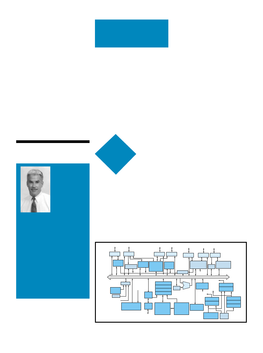
76
Issue 130 May 2001
CIRCUIT CELLAR
®
www.circuitcellar.com
emember the
Artist Formerly
Known as Prince?
Name changes are pretty
prevalent in the entertainment biz.
When searching the web, I found that
his mother used to call him “Skipper”
of all things. Anyway, AFKAP
arguably went a bit overboard when
he changed his name to an unpro-
nounceable icon.
Suppose he’d chosen an exclama-
tion point or an asterisk, or perhaps
most fitting, a dollar sign (something
with an ASCII code), maybe then it
wouldn’t have seemed so goofy. As it
was, the pictograph representing his
new name caused the ever-growing
electronic engines of publishing and
commerce to vapor lock.
What to do? According to
www.prince.org, O(+> is the proper
ASCIIfied version of his icon.
Not that I do a lot of field reporting,
but this thread prompts me to head
over to the local music emporium.
Where does this glyph fit in the col-
lating sequence, just after ABBA or
around ZZ Top? Would you file it
under A for AFKAP or O for O(+>?
I guess neither seems quite right
because there he sits, stubbornly
stuck under P for Prince with the rest
of the plain old “P” plebes. Oh well.
IT’S ALL IN A NAME
Some of you may have noticed that
the company formerly known as
Scenix (CFKAS) recently changed its
name, too.
Scenix didn’t go for the icon ploy,
although I imagine it’s only a matter
of time before another company does.
The new moniker is Ubicom, six ordi-
nary ASCII characters that won’t
upset anybody’s database. Better yet,
for no-nonsense types, the new name
actually says something about what it
does and clearly indicates its new
goal: ubiquitous communications.
The SX is a SeXy chip, but there are
lots of those around. Instead of being
small-fish Scenix in a big MCU pond,
Ubicom wants to be the shark in the
embedded Internet aquarium.
SILICON
UPDATE
What’s in a
name? In
showbusi-
ness a
name (or
at least what people
call you) can be the
catalyst for success,
or disaster. This
month, Tom peels off
the Ubicom label to
see how much Scenix
is left underneath.
Tom Cantrell
The Company Formerly
Known as Scenix
r
Port A
Port B
Port C
Port D
Port E
Port F
Port G
Timer 1
(T1)
Edge det.
Timer 2
(T2)
Parallel
slave
peripheral
Timer 0
(T0)
Interrupt
(2) Serializer
deserializer
ADC
Analog
comparator
SxCLK
Reset
Brown-
out
POR
*RST
Watchdog with
post-scaler
Internal
watchdog
clock
ISD
ISP
Writeback
Execute
Decode
Fetch
64-KB Flash
program
memory
16-KB RAM
program
memory
W
4-KB Data
memory
ALU
Real-time
timer
RTCLK
Divider
Multiplexer
Real-time
clock driver
CPU Core
clock
Divider
Multiplexer
Multiplexer
PLL
Divider
Divider
Divider
OSC
driver
System
clock
Figure 1—
It may sound familiar, but with rockin’ memory and techno SerDes (serializer/deserialer), the IP2022 is
no SX cover band.
www.circuitcellar.com
CIRCUIT CELLAR
®
Issue 130 May 2001
77
You’ve heard my take on this sub-
ject before. When it comes to adding
Internet functionality to embedded
applications, there are a few basic
ways to go.
First, there’s the “Honey, I shrunk
the PC” approach, which can be
described as a 32-bit CPU (typically
’x86, MIPS, or ARM) running a con-
ventional big-ticket OS (Windows,
Linux, or RTOS) with lots of memory.
The good news is that this scheme is
conceptually easy, boiling down to
packaging and marketing issues more
than hardware and software design
innovation. The bad news is that it
calls for a prodigious amount of sili-
con, which limits design-in to higher
priced products. Yes, thanks to the
march of silicon, it gets cheaper all
the time, but every penny counts in
embedded apps.
Specialized hardware solutions such
as Seiko and iReady chips (“’Net-in-a-
Chip,” Circuit Cellar 111) or turnkey
modules from the likes of Connect
One (“EZ-Mail Engine,” Circuit
Cellar
115) make much more efficient
use of silicon than desktop-in-drag 32-
bit solutions. On the other hand, they
sacrifice a degree of flexibility and
aren’t cheap because lower production
volume gives up some of the gate
count advantage.
Another option that offers you the
potential for both low-cost and flexi-
bility is shrink-wrapping Internet
functionality inside conventional
MCUs or DSPs. Both silicon efficien-
cy and high production volume cut
the price tag and software still gets to
call the shots.
Which “Mini-Me” web chip is
poised to climb the charts? Glad you
asked. Tap your feet to the latest tune
from CFKAS.
VARIATION ON A THEME
Unlike the company name, the
IP2022 (see Figure 1) is more than a
cosmetic change from its SX predeces-
sor. It still has the look and feel of
that chip, but it’s by no means identi-
cal, especially when you start poking
around under the hood.
Architecturally, you can still see
vestiges of the past in the W accumu-
lator, register file, pages, and so forth,
but it underwent a makeover (see
Figure 2). A 16-bit instruction yields
enough elbowroom to deliver more
ways (address registers and modes) to
easily get at larger chunks of memory.
The nonvolatile program memory is
a 64-KB (32K × 16) flash memory
organized into 8-KB pages (the range
of a branch without a page instruc-
tion) and 512-byte blocks (erase gran-
ularity). For data, there’s the 4-KB
RAM, as shown in the data and pro-
gram memory maps (see Figure 3).
A dedicated 16-level hardware
stack stores return addresses for sub-
routine calls. Program access to this
stack is made possible by mapping the
top entry into the software-accessible
CALLH and CALLL registers.
Exploiting this hook, you can use
push and pop instructions to imple-
ment an arbitrarily deep stack in data
RAM if necessary.
Another hallmark of the SX, blazing
jitter-free interrupt response, is car-
ried forward with the IP2022. It’s
enhanced with two sets of on-chip
shadow registers that allow one level
of interrupt nesting automatically
without the need for software inter-
vention. However, you should expect
to spend a few cycles figuring out
where the interrupt came from
because all 20 sources come home to
roost on a single interrupt vector.
As a Harvard design, the program
and data memories each have their
own bus. That works well if the only
accesses to program memory are
instruction fetches. However, espe-
cially in embedded apps, it’s a must to
store static data (i.e., constants, look-
up tables, text strings, and so on) in
the nonvolatile program memory.
Fortunately, the IP2022 makes it
easy to use the flash memory for not
only static data, but also dynamic
W Register
STATUS Register
MULH Register
SPDREG Register
INTSPD Register
XCFG Register
PCH/PCL Register
Interrupt register
IPCH/IPCL Register
INVECH/INTVECL Register
IPH/IPL Register
DPH/DPL Register
SPH/SPL Register
Program memory interface register
ADDRH/ADDRL Register
DATAH/DATAL Register
7
0
15
0
15
0
Address register
15
0
15
0
Figure 2—
The IP2022 is positively new age with mod-
ern niceties like address registers (IP, DP, and SP) and
a single-cycle multiplier.
Table 1—
Thanks to the SerDes, there’s more than one way— make that about half a dozen ways— for the IP2022 to shift a bit.
Mode
Encoding method
Differential or
Synchronization
EOP
Bit
Pre-emphasis
single-ended
register enabled
generation/detection
stuffing/unstuffing
outputs enabled
Disabled
None
No
No
No
No
No
10BaseT
Manchester
Single-ended
Yes
Yes
No
Yes
USB bus
NRZI
Differential
Yes
Yes
Yes
No
UART
None
Single-ended
No
No
No
No
I
2
C
None
Single-ended
No
No
No
No
SPI/
None
Single-ended
No
No
No
No
microwire
Figure 4—
Thanks to
an on-chip PLL, no
need to fuss with get-
ting a finicky 100-MHz
clock to work. Just bolt
on a 4-MHz crystal
and crank up the
speed instruction.
data updated at run time. It’s like hav-
ing an extra data EEPROM for pass-
words, calibration data, and more.
The ADDR(H/L) and DATA(H/L) reg-
isters along with simple FREAD,
FWRITE (16-bit words), and FERASE
(512-byte block) instructions and a
built-in charge pump make flash
memory access straightforward.
However, note that the guaranteed
write and erase endurance is only
1000 cycles. Avoiding burnt-out bits
78
Issue 130 May 2001
www.circuitcellar.com
CIRCUIT CELLAR
®
requires software to utilize techniques
such as wear leveling for frequently
written data.
SPEED FREAK
Between the 32K × 16 flash memo-
ry and 4-KB RAM is something new,
an extra 8K × 16 RAM. What’s that all
about, you ask?
Here’s the story. Although the
IP2022 carries forward the SX aggres-
sive, triple-digit-clock-rate-capable,
(100-MHz) four-stage pipeline imple-
mentation, the capability to run at
full speed out of flash memory has
been conceded to the realities of IC
fabrication.
It turns out that designing a flash
memory cell with a few nanosecond
access time is no amazing feat, calling
for a highly tuned and tweaked cus-
tom design. Unfortunately, as a fab-
less IC company, Ubicom is much
better off relying on the standard flash
memory cell offered by its foundry to
facilitate easy migration to each new
process generation.
So, the IP2022 only runs at up to 40
MHz out of flash memory, which
admittedly is right up there with the
fastest 8-bit chips. Fully exploiting
the MIPS on tap is accomplished by
moving speed-critical routines into
the aforementioned 8K × 16 RAM,
which runs at full speed.
In essence, it’s kind of a roll-your-
own cache in which software deter-
mines what gets cached and when.
For your embedded applications, this
is much improved over a real cache
that comes with all kinds of baggage
in the form of timing uncertainties
(hit or miss) and overhead (cache line
OSC1
OSC2
OSC
Driver
Pre-
scaler
50X PLL
clock
multiplier
Post-
scaler
PLL Bypass
SPDREG
Divider
RTCLK1
RTCLK2
RTCLK
Driver
CPU
core
ADCLK
TMR0
(+DIV)
RTCLK
(+DIV)
TMR1
(+DIV)
TMR2
(+DIV)
Serial
PLL clock
0×000
0×080
0×100
0×FFF
128
Special-purpose
registers
128
Global registers
3840 Bytes of
data memory
7
0
Figure 3—
On-chip memory includes 32K × 16 flash
memory, 4K × 8 data RAM (including the general-pur-
pose and special function registers) and a unique 8K ×
16 high-speed program RAM.
Word
address
0×0000
0×2000
0×8000
0×A000
0×C000
0×E000
0×FFFF
Byte
address
0×0000
0×4000
0×10000
0×14000
0×18000
0×1C000
0×1FFFF
Program RAM
Reserved
Flash memory
Flash memory
Flash memory
Flash memory
15
0
fills and spills). The RAM can also be
used for data, although access (via
dedicated IREAD and IWRITE
instructions) is much slower (four
clocks) than for the single-cycle, 4-KB,
data-only RAM.
Clocking (see Figure 4) starts with
two oscillator inputs, one that is high-
speed (4-MHz), feeding an on-chip
50X PLL multiplier, and one that is
low-speed (32-kHz watch crystal). The
new speed instruction not only
accommodates the memory hierarchy,
but also serves as the basis for power
management. It selects the clock
source, enables and disables the oscil-
lator and PLL, and sets a 16-stage,
power-of-two clock divisor, yielding a
system clock range covering 780 kHz
to 100 MHz.
There’s also an INTSPD register
that automatically does the same
thing as a speed instruction when an
interrupt occurs. A likely scenario is
to have background software run at
low speed to save power, automatical-
ly shifting into high gear when an
interrupt occurs. Upon return, there’s
an option to leave the speed instruc-
tion as is or restore it to the pre-inter-
rupt setting.
THE USUAL SUSPECTS
The IP2022 includes a healthy com-
plement of built-in glue logic and I/O
functions. After all, when it gets on
the ’Net, presumably it’s supposed to
do something useful besides just
yakking with other computers.
Although the chip runs on a 2.3- to
2.7-V supply, the I/O pins are 5-V tol-
erant and four of them (Port A) fea-
ture a whopping 24-mA drive capabil-
ity. Eight pins (Port B) can be used as
external interrupt inputs with pro-
grammable edge detection. A nice
touch is that the Port B logic is asyn-
chronous, which means that an exter-
nal interrupt can be used to wake up
the chip even if the clock is disabled.
With a traditional watchdog timer
and 8-bit timer with an 8-bit prescaler
running off the 32-kHz oscillator, the
latter is a natural for use as a real-
time (HH:MM:SS) clock. In addition,
there’s also an 8-bit timer with a 15-
bit prescaler and two sophisticated
16-bit timers with 8-bit prescalers,
the latter gussied-up with timer,
PWM, and Capture and Compare
modes with programmable rising-,
falling-, or any-edge trigger.
These days, it’s hard to find an
MCU that doesn’t offer some analog
capability, and the IP2022 is no excep-
tion. There’s an eight-channel, 10-bit
Receive polarity
reversal bit
SxRXP
Input
Serial PLL clock
OSC clock
RTCLK
Clock/data
separation
and
start
condition
detection
Synchronization
pattern
register
(SxRSYNC)
SxRXP
Input
SxRXM
Input
EOP
Detection
UART Clock
divider
Clock
Data
Receive data
SxCLK
Receive
clock
Transmit
clock
EOP
www.circuitcellar.com
CIRCUIT CELLAR
®
Issue 130 May 2001
79
EOP
Receive
count
register
(SxRCNT)
>
Receive
data
Receive
clock
Receive
count
register
(SxRCNT)
>
Receive
interrupt
Data bus
Transmit
configuration
register
(SxTCFG)
Transmit
interrupt
Transmit
buffer
register
(SxTBUF)
Transmit
clock
>
>
Data
encoder
Pre-
emphasis
EOP
Generator
Data bus
SxOE
SxTXM
SxTXP
SxTXME
SxTXPE
a)
c)
b)
Figure 5—
Each of the SerDes units consists of transmit and receive shifters plus protocol-specific logic. The hardware does the hard part, software handles the rest.

80
Issue 130 May 2001
CIRCUIT CELLAR
®
www.circuitcellar.com
ADC (Port G) with 48-kHz through-
put and right- or left-justification
along with an analog comparator with
optional 50-mV hysteresis. All super-
visor chip functions are there, includ-
ing watchdog timer, brownout detec-
tion, and power-on reset.
The IP2022 would make an excel-
lent coprocessor, off-loading the real-
time dirty work that tends to bring
big-ticket CPUs to their knees. To
that end, Port C and Port D are sup-
plemented with a Parallel Slave
Peripheral mode utilizing dedicated
control lines *CS, R/W, and *HOLD.
From the perspective of a host CPU,
the IP2022 easily mimics a regular 8-
or 16-bit peripheral without imposing
critical timing or software gyrations
on either chip.
BREAKFAST OF CHAMPIONS
Completing the com-centric
makeover, the IP2022 incorporates a
pair of intriguing serializer/deserializ-
er (i.e., SerDes) units. Just think shift
registers on steroids, and take a look
at Figure 5.
By now, we’re all familiar with the
arguments related to hardware versus
software. It’s not a new concept;
somewhere I’ve got an Intel “Software
UART” app note from 20 years ago, a
cute trick that legions of designers
have exploited in the years since.
Indeed, the original SX marketing
strategy was based on the idea of
replacing dedicated hardware with
software virtual peripherals.
However, doing serial ports purely
in software does have its disadvan-
tages and frustrations. The grunt
work simply gets in the way of doing
more important things and can
become a surprisingly big hassle,
especially as the data rate increases.
Sure, it’s possible to pull off a
UART or other simple interface in
software, but what about upping the
ante? With 100 MIPS, it’s possible to
contemplate going further with, for
example, USB or Ethernet. However,
it’s not going to be pretty, and remem-
ber, all it takes is one critical timing
spec to be a showstopper.
I’ve often thought that what the
world needs is an approach some-
where in-between pure hardware and
pure software solutions. The goal is
something more transistor-efficient
and flexible than hardwired logic, but
less burdensome than doing every-
thing in software.
Well, that’s exactly what the SerDes
is all about. I’ve seen the bit processor
strategy employed on some of the
high-end network processor super-
chips, but now it’s come to the MCU
on your block. Thanks to the SerDes,
the IP2022 doesn’t even work up a
sweat over stuff like UART, SPI, or
I
2
C, and realistically has a chance of
handling USB and even Ethernet. You
can see proof in Table 1.
The shift registers cut the drudge
work by a factor greater than eight,
but there’s more to it than that. To
handle the critical timing aspects of
Ethernet and USB, the SerDes also
incorporates a dash of protocol-specif-
ic hardware that takes care of the
most difficult tasks like detecting the
start and end of packets and encoding
or decoding the data.
Each SerDes includes eight pins to
accommodate the variety of differen-
tial data- and protocol-specific signals.
For example, USB requires a couple of
extra pins to detect the EOP condition
and Ethernet needs an enable line for
the external magnetics.
The scheme doesn’t get software
totally and completely off the hook.
In the case of USB, you have to form
the packets, handle CRCs, and check
for certain special conditions such as
bus suspend or reset. Ethernet calls
for a little bit more hand-holding,
such as dealing with collisions and
other link problems (polarity reversal
and jabber detection), but it is still
well within reach.
GNU DAY YESTERDAY
It’s ironic that the hot setup is a
chip with roots that go way back, run-
ning a tool chain that’s no spring
chicken either.
The fact is, the GNU tool chain (C
compiler, assembler, debugger, and
IDE) is becoming a major player in
embedded apps, and not just for 32-
bits. The announcement that the
IP2022 will be supported with Red
Hat GNUPro tools certainly rein-
forces the trend.
Circuit Cellar is available in
Experience your Dream Computer
RELIABLE, POWERFUL WORKSTATION AT
AN UNBELIEVABLY LOW PRICE. WITH 20GB
HD & 17” MONITOR.
CREATE AUDIO & DATA CDs WITH EASE!
CREATIVE LABS CDRW & 30GB HD DELIVERS
HIGH PERFORMANCE ON A BUDGET.
82
Issue 130 May 2001
CIRCUIT CELLAR
®
www.circuitcellar.com
+972-9-766-0456
Fax: +972-9-766-0461
www.connectone.com
i1000 ichip
iReady Corp.
(408) 330-9450
Fax: (408) 330-9451
www.ireadyco.com
GNUPro tools
Red Hat, Inc.
(919) 547-0012
Fax: (919) 547-0024
www.redhat.com
IP2022 Internet processor
Ubicom, Inc.
(650) 210-1500
Fax: (650) 210-8715
www.ubicom.com
SOURCES
Tom Cantrell has been working on
chip, board, and systems design and
marketing for several years. You may
reach him by e-mail at
tom.cantrell@circuitcellar.com.
As I write this, I don’t yet have the
IP2022 tools in hand. It will be inter-
esting to see how well the compiler
handles the relatively small footprint.
No doubt the debugger will take
advantage of the IP2022 serial debug
and programming port.
Getting on the ’Net is the prime
directive. Ubicom has all of the virtu-
al peripheral drivers for Ethernet,
USB, UART, and the TCP/IP stack
you’ll need. The price (free) is defi-
nitely right. I also hear talk of a free
RTOS in the works. They’re giving
away all the razors to sell you $13 (at
10K) IP2022 blades.
2001, A ’NET ODYSSEY
Connecting real-world stuff like
cars, homes, and appliances is what’s
going to push the ’Net beyond being
little more than a glorified BBS.
I recently saw a report about a gadg-
et designed to help consumers moni-
tor and budget energy use in the
home by establishing two-way com-
munication with the power company
over the ’Net. Judging from the head-
lines about the lights going out, I may
need one of those myself before long.
The bad news is that the unit’s 32-
bit CPU and megabytes of memory
undermine its turnkey consumer pre-
tensions. That’s just what you need,
another power-sucking 24/7 bloat box
to remind you not to waste power.
The dot-coms may have crashed,
but the real ’Net fun is just beginning.
Chips like the IP2022 with Ethernet
and USB will help embedded apps get
online. Communication, computa-
tion, and control all in one low-cost,
low-power chip is music to my ears.
I can’t remember the artist’s name,
but hey, it’s got a good beat and I can
dance to it.
I
CIRCUIT CELLAR
Test Y
Your E
EQ
What’s your EQ?
—The answers
and 4 additional questions and
answers are posted at
www.circuitcellar.com
You may contact the quizmasters
at eq@circuitcellar.com
8
more EQ
questions
each month in
Circuit Cellar Online
see pg. 4
Problem 1
— Given the following prototype:
int compact (int *p, int size);
write a function that will take a sorted array
with some elements duplicated, and com-
pact the array by removing the duplicates,
returning the new length of the array. For
example, if p points to an array containing
1, 3, 7, 7, 8, 9, 9, 9, 10, when the function
returns, the contents of p should be: 1, 3,
7, 8, 9, 10, with a length of 6 returned.
Contributed by Wael Badaway
Problem 2
— What are the basic functions
provided by a computer file sys
tem?
Contributed by Dave Tweed
Problem 3
— We know that both silicon and ger-
manium are semiconductors used in discrete
devices. But why is silicon alone used in IC fab-
rication and not germanium?
Contributed by Naveen PN
Problem 4
— How can a 555 timer IC be used
as an inverter? What are its advantages?
Contributed by Naveen PN

www.circuitcellar.com
CIRCUIT CELLAR
®
Issue 130 May 2001
83
Insert-ready sub-mini SBCs (small as 47x55 mm.) supporting the
Philips
achieved via GND circuitry, 6 to 8 layer PCB, by-
32 KB to 8 MB external SRAM & Flash (controller-dependent)
FlashTools enable on-board in-system (ISP) programming
C & CAN interfaces; ADC; Chip-Select signals
■ 255 Ericksen Avenue ■ Bainbridge Island, WA ■ USA 98110
IDEA BOX
THE
DIRECTORY
OF
PRODUCTS AND
SERVICES
AD FORMAT
: Advertisers must furnish digital submission sheet and digital files that meet the specifications on the digital submission sheet.
ALL TEXT AND OTHER ELEMENTS MUST FIT WITHIN A 2
″″ ××
3
″″
FORMAT
. Call for current rate and deadline information. Send your disk and digital submis-
sion sheet to: IDEA BOX, Circuit Cellar, 4 Park Street, Vernon, CT 06066 or email kc@circuitcellar.com. For more information call Kevin Dows at (860) 872-3064.
Suppliers Directory now available online. Check out our web site
www.circuitcellar.com to see who has what and how to get it!
84
Issue 130 May 2001
CIRCUIT CELLAR
®
www.circuitcellar.com

www.circuitcellar.com
CIRCUIT CELLAR
®
Issue 130 May 2001
85
Scottsdale, Arizona
Ph: 480.998.3503
Fx: 480.998.3504
Resistance Substitution Device
Order
on-line for
FREE shipping!
Need to quickly get up to speed with the
PICmicro
172 Harvard Road
Waterloo, ON, N2J 3V3
Canada
519.886.4462
519.886.4253(fax)
86
Issue 131 June 2001
CIRCUIT CELLAR
®
www.circuitcellar.com
For acquisition and control of digital and analog signals.
High speed Serial Port Interface
24 digital I/O (TTL compatible)
11 Analog Channels with 12 bit ADC
4 channels with signal conditioning
Embedded stepper motor controller
32 bit DLL
Control up to 16 stepper motors simultaneously
Up to 8500 Steps/sec with linear Accel/Decel.
Chopper driver up to 48V/2A for 4,5or 6 wire motors.
Software Winding Current Setup.
Shaft encoder input , external driver capabilities.
Internal FIFO for linear, cubic or spline Interpolation.
24 digital I/O,2 SPI, 11 analog channels on-board.
32 bit DLL with examples in VC++,VBasic and Delphi.
9 Channel Data
Loggers from
US$400. Ask us, or
visit our web site.

www.circuitcellar.com
CIRCUIT CELLAR
®
Issue 131 June 2001
87
www.circuitcellar.com
CIRCUIT CELLAR
®
Issue 131 June 2001
89
• Full duplex
• 422 or 485 4 wire
• Short haul modem
Connecticut microComputer, Inc.
PO BOX 186, Brookfield,CT 06804
(203)740-9890 Fax:(203)775-4595
Easy to use converter adapts any
....by using real-time emulators.
HC12, HC11
8051
C166
C500
ST10
Super10
Philips XA
68300 family
Ubicom
90
Issue 131 June 2001
CIRCUIT CELLAR
®
www.circuitcellar.com
PC Based Data Acquisition & Control Products
PCI-9812, 20 MHz Simultaneous
4-Ch Analog Input Card
PCI-7300A, Ultra-High Speed 32-Ch
Digital I/O Card
AILS. Much broader selection online!

www.circuitcellar.com
CIRCUIT CELLAR
®
Issue 131 June 2001
91
Email: sales@picofab.net
92
Issue 131 June 2001
CIRCUIT CELLAR
®
www.circuitcellar.com
Integrated Development Systems:
Compilers, Simulators, Programmers,
Non-intrusive, with trace feature, hardware unconditional & complex
breakpoints, triggers, programmable clock, memory mapping &
banking, full project & source level support for C compilers…
2900-1 Crescent Drive
Tallahassee, FL 32308
Options: 8-ch 12-bit ADC, flash disks up to 288 MB, 1 RS-485
Tiny Size, Low Power: 2”x2.6”, 5V @ 200 mA at full speed.
Visit http://www.bagotronix.com for info, prices, and FAQs
• Easy to Use
• Low Cost
• Low Power
• Tiny Size
• High Speed
• DOS Environment
www.circuitcellar.com
CIRCUIT CELLAR
®
Issue 131 June 2001
93
94
Issue 131 June 2001
CIRCUIT CELLAR
®
www.circuitcellar.com
56&RQWUROOHGRU&DQQHG&\FOHG&RQWUROOHG
6KRUW&LUFXLWDQG2YHU7HPS3URWHFWLRQ
3URJUDPPDEOHELWRSWLFDOO\LVRODWHGLQSXWV
%XLOWLQ$FFHOHUDWLRQ'HFHOHUDWLRQUDPSLQJ
6RIWZDUH&XUUHQW$GMXVWPHQWYLD56
• Design, PCB Fabrication & Assembly
• DS, Multi-Layer, SMT & RF PCBs
• In-house CAM & Photo Plotting and
Superior Quality at Competitive Prices
"...your product was delivered on
schedule and was of the highest quality."
R.R. Bell Atlantic Test Systems
7845-M Airpark Rd., Gaithersburg, MD 20879
Fax: (301) 990-6715 BBS: (301) 990-9628

ADVERTISER’S
www.circuitcellar.com
CIRCUIT CELLAR
®
Issue 130 May 2001
95
INDEX
72
ADAC
93
Abacom Technologies
92
Abia Technology
85
Ability Systems Corp.
86
ActiveWire, Inc.
13,78
Advanced Transdata Corp.
45
All Electronics Corp.
9
Amulet Technologies
84
Andromeda Research
86
AP Circuits
63
Arcom Control Systems
39
Atmel Corporation
92
Bagotronix, Inc.
84
Basic Micro
85
Bay Area Circuits
85
CCS-Custom Computer Services
94
CSMicro Systems
94
Capital Electro-Circuits, Inc
93
Cermetek Microelectronics, Inc.
90
Circuit Specialists, Inc.
86
Conitec
37,89
Connecticut mircoComputer Inc.
48,49
Convergence University
85
Copeland Electronics Inc.
86
Cyberpak Co.
23
Cygnal Integrated Products
92
Data Design Corp.
C4
Dataman Programmers, Inc.
91
Decade Engineering
34
Design Logic 2001 Contest
The Advertiser’s Index with links to their web sites is located at www.circuitceller.com under the current issue.
Page
87 Designtech Engineering
81
Dreamtech Computers
36
Earth Computer Technologies
74
ECD (Electronic Controls Design)
84
EE Tools
(Electronic Engineering Tools)
7
EEGLOBE Inc.
18
EMAC, Inc.
74
Engineering Express
84
FDI-Future Designs, Inc.
42
General Software
85
HVW Technologies Inc.
84
Hagstrom Electronics
89
IMAGEcraft
69
IndustroLogic,Inc.
91,93
Intec Automation, Inc.
65
Interactive Image Technologies Ltd.
91
Intronics, Inc.
42,87
JK microsystems
69
JR Kerr Automation & Engineering
57
Jameco
66,68,88
LLH Technology Publishing
85
LabMetric, Inc.
89,90
Laipac Technology, Inc.
15,94
Lemos International
2
Link Instruments
85
Lynxmotion, Inc.
90
MaxStream
91
MCC (Micro Computer Control)
83
MetaLink Corporation
88
MJS Consulting
87,88
Micro Digital Inc
93
microEngineering Labs, Inc.
32
Micromint Inc.
69
Midwest Micro-Tek
94
Mosaic Industries Inc.
58,75
MVS
91
Mylydia Inc.
33
Netburner
88,94
Netmedia, Inc.
89
Nohau Corp.
87,89,90
OKW
64
Ontrak Control Systems
92
PCB Express, Inc.
C2
Parallax, Inc.
90
Peter H. Anderson
83
Phytec America LLC
92
Phyton, Inc.
91
Picofab Inc.
91
Prairie Digital Inc.
88
Pulsar Inc.
84
Quadravox Inc.
84
R.E.Smith
89
RLC Enterprises, Inc.
86
RMV Electronics Inc.
55
Rabbit Semiconductor
66
Remote Processing
85
SMTH Circuits
38,53
Saelig Company
5
Scott Edwards Electronics Inc.
88
Sealevel Systems Inc.
91
Senix Corp.
94
Sigg Industries
83
Signum Systems
85
Sirius MicroSystems
87
SmartHome.com
47
Solutions Cubed
83
Square 1 Electronics
90
Streetrod Digital
94
Tal Technologies
90
Tech Systems
64,79
Technologic Systems
86
Technological Arts
C3
Tech Tools
89
Tern Inc.
73
Texas Instruments
37
Trilogy Design
92
Vantec
92
Vetra Systems Corp.
86
Weeder Technologies
1
Wilke Technology GmbH
75
Xelos
93
Xilor Inc.
87
Z-World
91
Zagros Robotics
83
Zanthic Technologies Inc.
25
ZiLOG
High-Performance Oscilloscope Amplitude Calibrator
USB, FTDI Style
Scan 3-D
SCUBA Dive Monitor
Wireless Data Link
Electronics Lab Design2K Winner
I Above the Ground Plane
: Can’t Set Your Clock
I From the Bench
: Intelligible HUBbub: Ethernet Home Networking
I Silicon Update
: Power Tripped
I Applied PCs:
Working with a Player
Page
Page
Page
Communications
PREVIEW
131

f I were a better prognosticator, I suppose my stock portfolio wouldn’t be down the toilet. I’ve certainly
foreseen the big events in history. I didn’t miss the significance of inventions like the personal computer,
the VCR, or the cell phone but I have missed some major consumer-electronic milestones. This hit or miss
wisdom makes me wonder if my personal purchasing habits bias my assessment, or if I simply ignore those
inventions that I don’t personally need (I’m not the kind of guy who walks around with an MP3 player in his pocket). Worse yet, do I
have to wait until some big Japanese manufacturer gears up and makes it so easy to use that I can’t ignore it anymore?
The rapid pace of electronic designs today has created a new sort of faster-moving consumer-electronics company. While tradi-
tional products like VCRs, video games, CD players, answering machines, and cordless phones remain dominated by the same
Japanese firms for the last 25 years, a host of new digital gadgets are being made by firms outside the usual consumer-electronics
world of Sony, Panasonic, and NEC. Most of these products are spin-offs from the computer industry. Others, such as digital cam-
eras and DVD drives, have their roots in consumer electronics but have nevertheless been adopted by PC users first.
Although past buying choices focused on brand identifications like an Olympus camera, Sony radio, or Nintendo game console,
today we are just as likely to get a Hewlett-Packard digital camera, a 3Com Internet radio, a Palm PDA, or a Microsoft game con-
sole. Even Intel sells consumer-electronic products these days. We have come to think of digital cameras, portable assistants, and
even MP3 players as PC accessories. It not only influences how we use them, it defines which firms we buy them from. These new
digital devices are not an evolutionary stage in an existing product. They are entirely new products. We buy them because of their
innovation, not their brand history.
At the same time, we shouldn’t get fat, dumb, and happy thinking that the present market advantage will last forever. The giant
Japanese consumer-electronics firms haven’t quite gotten their act together yet, but the bears will awaken.
First of all, Japanese manufacturers are willing to operate at much lower profit margins than American competitors. Market satu-
ration and low profits are what drove American TV production to Asian shores. Right now these new digital devices are barely 10%
of consumer-electronics sales in America. This is a superficial blip on the U.S.-Japanese trade radar and not enough to sustain the
apparent trend.
What American business really has to worry about is its “geek mentality.” This present shift towards products from the mostly
American computer companies isn’t necessarily permanent. So far, most of it has been sold to gear-heads and gadget freaks like
us (i.e., knowledgeable PC users familiar with computer industry brands). You’ve also heard me comment many times about how
complicated all this new equipment and software remains. If these products are to be accepted in the mass market, customers will
expect them to be easy to use. An Internet radio should operate, well, like a radio. Although I’m optimistic that small innovative
American companies might have read the book on making the transition to a mass market, it is the established consumer-electron-
ics giants that wrote it. Regardless of the fact that 12:00 has been flashing on your VCR for the last 15 years, they do know how to
make electronics seem less complicated.
The only salvation for our collective future may be that these digital gadgets are different. Like the PC itself, more of the profit is
in software and related services, not the commodity hardware itself. If the innovative companies that designed these products are
going to survive the long haul, they should not try to go head-to-head against Japanese industry giants at a hardware level.
Instead, they should concentrate on selling designs, content, and software licenses. The successful corporate strategy for the
future may be knowing that, even though it says Panasonic all over the brand label, Hewlett-Packard or Compaq is cashing the
check for the IP inside.
Watch Out for the Bears
INTERRUPT
i
steve.ciarcia@circuitcellar.com
PRIORITY
96
Issue 130 May 2001
CIRCUIT CELLAR
®
www.circuitcellar.com
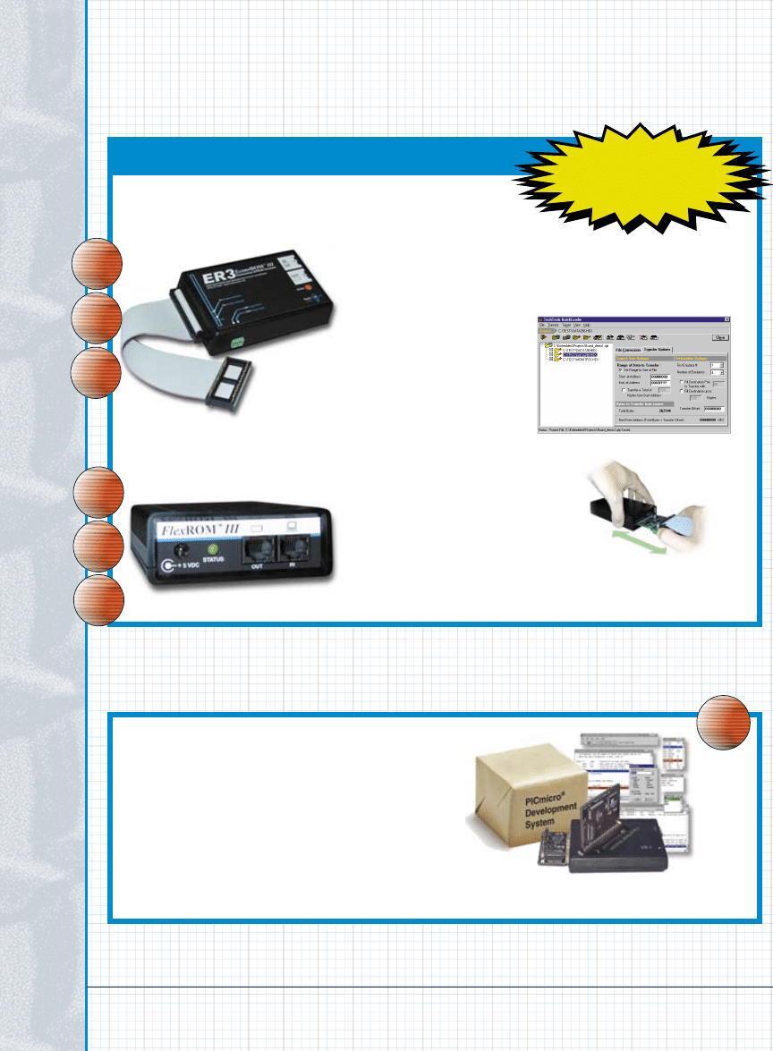
In-Circuit Firmware Development with
evelopment tools from TechTools
ER3 will speed up your firmware
development by eliminating the need
to remove-erase-program and re-
devices plug into the EPROM
socket on your target board
We provide software that loads your
firmware code into the emulator in a matter of
seconds! No more waiting for the eraser or
EPROM programmer. No more “debugging” bent
FlexROM emulators provide engineers with a flexible
development tool for any Embedded project that uses an
external FLASH, EPROM or SRAM device.
see the Target’s address fetches with FR3’s Hardware
FR3 is a Flexible, in-circuit memory Emulator with instrumentation.
ER3 is designed for quick, in-circuit firmware test cycles.
TechTools Complete Development System with integrated
Orders received by 4pm will normally be despatched same day.
• Plugs straight into parallel port of PC or
• Programs and verifies at 2, 2.7, 3.3 & 5V
• True no-adaptor programming up to 48
• Free universal 44 pin PLCC adaptor
• Built-in world standard PSU - for go-
• Package adaptors available for TSOP,
• Programs 8 and 16 bit EPROMs,
EEPROMs, PEROMs, 5 and 12V FLASH,
Boot-Block FLASH, PICs, 8751
microcontrollers and more
• Rechargeable battery power for total
• All-in-one price includes emulation
leads, AC charger, PC software, spare
library ROM, user-friendly manual
• Supplied fully charged and ready to use
• Programs wide range of 20 and 24 pin
logic devices from the major GAL vendors
• Supports JEDEC files from all popular
• 3 year parts and labor warranty
• Windows/DOS software included
• Free technical support for life
• Next day delivery - always in stock
Order via credit card hotline - phone
today, use tomorrow.
If you do not agree that these truly are the
most powerful portable programmers you can
Wyszukiwarka
Podobne podstrony:
więcej podobnych podstron
